US5948176A - Cadmium-free junction fabrication process for CuInSe2 thin film solar cells - Google Patents
Cadmium-free junction fabrication process for CuInSe2 thin film solar cellsDownload PDFInfo
- Publication number
- US5948176A US5948176AUS08/939,844US93984497AUS5948176AUS 5948176 AUS5948176 AUS 5948176AUS 93984497 AUS93984497 AUS 93984497AUS 5948176 AUS5948176 AUS 5948176A
- Authority
- US
- United States
- Prior art keywords
- copper indium
- layer
- indium diselenide
- zinc chloride
- zinc oxide
- Prior art date
- Legal status (The legal status is an assumption and is not a legal conclusion. Google has not performed a legal analysis and makes no representation as to the accuracy of the status listed.)
- Expired - Lifetime
Links
- 238000000034methodMethods0.000titleclaimsabstractdescription29
- 239000010409thin filmSubstances0.000titleclaimsabstractdescription16
- 238000004519manufacturing processMethods0.000titledescription9
- XLOMVQKBTHCTTD-UHFFFAOYSA-NZinc monoxideChemical compound[Zn]=OXLOMVQKBTHCTTD-UHFFFAOYSA-N0.000claimsabstractdescription78
- JIAARYAFYJHUJI-UHFFFAOYSA-Lzinc dichlorideChemical compound[Cl-].[Cl-].[Zn+2]JIAARYAFYJHUJI-UHFFFAOYSA-L0.000claimsabstractdescription64
- KTSFMFGEAAANTF-UHFFFAOYSA-N[Cu].[Se].[Se].[In]Chemical compound[Cu].[Se].[Se].[In]KTSFMFGEAAANTF-UHFFFAOYSA-N0.000claimsabstractdescription46
- 239000011787zinc oxideSubstances0.000claimsabstractdescription39
- 235000005074zinc chlorideNutrition0.000claimsabstractdescription32
- 239000011592zinc chlorideSubstances0.000claimsabstractdescription32
- 239000004065semiconductorSubstances0.000claimsabstractdescription18
- 238000009792diffusion processMethods0.000claimsabstractdescription13
- 150000004820halidesChemical class0.000claimsabstractdescription9
- 239000007787solidSubstances0.000claimsabstractdescription7
- 239000010408filmSubstances0.000claimsdescription26
- OKKJLVBELUTLKV-UHFFFAOYSA-NMethanolChemical compoundOCOKKJLVBELUTLKV-UHFFFAOYSA-N0.000claimsdescription18
- VEXZGXHMUGYJMC-UHFFFAOYSA-NHydrochloric acidChemical compoundClVEXZGXHMUGYJMC-UHFFFAOYSA-N0.000claimsdescription6
- 238000000151depositionMethods0.000claimsdescription5
- 229910052751metalInorganic materials0.000claimsdescription4
- 239000002184metalSubstances0.000claimsdescription4
- 238000005530etchingMethods0.000claimsdescription3
- 238000000859sublimationMethods0.000claimsdescription3
- 230000008022sublimationEffects0.000claimsdescription3
- XLYOFNOQVPJJNP-UHFFFAOYSA-NwaterChemical compoundOXLYOFNOQVPJJNP-UHFFFAOYSA-N0.000claimsdescription3
- 238000005229chemical vapour depositionMethods0.000claimsdescription2
- 239000008367deionised waterSubstances0.000claimsdescription2
- 229910021641deionized waterInorganic materials0.000claimsdescription2
- 238000004140cleaningMethods0.000claims2
- 239000012808vapor phaseSubstances0.000claims1
- 239000000463materialSubstances0.000abstractdescription12
- 229910052793cadmiumInorganic materials0.000abstractdescription5
- BDOSMKKIYDKNTQ-UHFFFAOYSA-Ncadmium atomChemical compound[Cd]BDOSMKKIYDKNTQ-UHFFFAOYSA-N0.000abstractdescription5
- HCHKCACWOHOZIP-UHFFFAOYSA-NZincChemical compound[Zn]HCHKCACWOHOZIP-UHFFFAOYSA-N0.000abstractdescription3
- 229910052725zincInorganic materials0.000abstractdescription3
- 239000011701zincSubstances0.000abstractdescription3
- ZAMOUSCENKQFHK-UHFFFAOYSA-NChlorine atomChemical compound[Cl]ZAMOUSCENKQFHK-UHFFFAOYSA-N0.000abstractdescription2
- 229910052801chlorineInorganic materials0.000abstractdescription2
- 239000000460chlorineSubstances0.000abstractdescription2
- -1chlorineChemical class0.000abstract1
- 229910052980cadmium sulfideInorganic materials0.000description10
- RYGMFSIKBFXOCR-UHFFFAOYSA-NCopperChemical compound[Cu]RYGMFSIKBFXOCR-UHFFFAOYSA-N0.000description9
- 229910052802copperInorganic materials0.000description9
- 239000010949copperSubstances0.000description9
- 239000000243solutionSubstances0.000description8
- 241000276498Pollachius virensSpecies0.000description7
- 238000006243chemical reactionMethods0.000description5
- WUPHOULIZUERAE-UHFFFAOYSA-N3-(oxolan-2-yl)propanoic acidChemical compoundOC(=O)CCC1CCCO1WUPHOULIZUERAE-UHFFFAOYSA-N0.000description4
- GYHNNYVSQQEPJS-UHFFFAOYSA-NGalliumChemical compound[Ga]GYHNNYVSQQEPJS-UHFFFAOYSA-N0.000description4
- 230000015572biosynthetic processEffects0.000description4
- 239000011669seleniumSubstances0.000description4
- 239000000758substrateSubstances0.000description4
- UGZADUVQMDAIAO-UHFFFAOYSA-Lzinc hydroxideChemical compound[OH-].[OH-].[Zn+2]UGZADUVQMDAIAO-UHFFFAOYSA-L0.000description4
- 229940007718zinc hydroxideDrugs0.000description4
- 229910021511zinc hydroxideInorganic materials0.000description4
- 229910052770UraniumInorganic materials0.000description3
- 238000005234chemical depositionMethods0.000description3
- 230000008020evaporationEffects0.000description3
- 238000001704evaporationMethods0.000description3
- 229910052733galliumInorganic materials0.000description3
- 229910052738indiumInorganic materials0.000description3
- APFVFJFRJDLVQX-UHFFFAOYSA-Nindium atomChemical compound[In]APFVFJFRJDLVQX-UHFFFAOYSA-N0.000description3
- XKRFYHLGVUSROY-UHFFFAOYSA-NArgonChemical compound[Ar]XKRFYHLGVUSROY-UHFFFAOYSA-N0.000description2
- BUGBHKTXTAQXES-UHFFFAOYSA-NSeleniumChemical compound[Se]BUGBHKTXTAQXES-UHFFFAOYSA-N0.000description2
- BOKSKTADHYXBBM-UHFFFAOYSA-L[Cl-].[Cl-].[Zn+2].OCChemical compound[Cl-].[Cl-].[Zn+2].OCBOKSKTADHYXBBM-UHFFFAOYSA-L0.000description2
- 229910052782aluminiumInorganic materials0.000description2
- XAGFODPZIPBFFR-UHFFFAOYSA-NaluminiumChemical compound[Al]XAGFODPZIPBFFR-UHFFFAOYSA-N0.000description2
- 230000002950deficientEffects0.000description2
- 229910052711seleniumInorganic materials0.000description2
- 238000005118spray pyrolysisMethods0.000description2
- 238000004544sputter depositionMethods0.000description2
- 239000000126substanceSubstances0.000description2
- UMGDCJDMYOKAJW-UHFFFAOYSA-NthioureaChemical compoundNC(N)=SUMGDCJDMYOKAJW-UHFFFAOYSA-N0.000description2
- VHUUQVKOLVNVRT-UHFFFAOYSA-NAmmonium hydroxideChemical compound[NH4+].[OH-]VHUUQVKOLVNVRT-UHFFFAOYSA-N0.000description1
- WKBOTKDWSSQWDR-UHFFFAOYSA-NBromine atomChemical compound[Br]WKBOTKDWSSQWDR-UHFFFAOYSA-N0.000description1
- VEXZGXHMUGYJMC-UHFFFAOYSA-MChloride anionChemical compound[Cl-]VEXZGXHMUGYJMC-UHFFFAOYSA-M0.000description1
- 229910000807Ga alloyInorganic materials0.000description1
- ZOKXTWBITQBERF-UHFFFAOYSA-NMolybdenumChemical compound[Mo]ZOKXTWBITQBERF-UHFFFAOYSA-N0.000description1
- NSEQHAPSDIEVCD-UHFFFAOYSA-NN.[Zn+2]Chemical compoundN.[Zn+2]NSEQHAPSDIEVCD-UHFFFAOYSA-N0.000description1
- 240000008881Oenanthe javanicaSpecies0.000description1
- 229910000796S alloyInorganic materials0.000description1
- NINIDFKCEFEMDL-UHFFFAOYSA-NSulfurChemical compound[S]NINIDFKCEFEMDL-UHFFFAOYSA-N0.000description1
- GSEJCLTVZPLZKY-UHFFFAOYSA-NTriethanolamineChemical compoundOCCN(CCO)CCOGSEJCLTVZPLZKY-UHFFFAOYSA-N0.000description1
- XSQUKJJJFZCRTK-UHFFFAOYSA-NUreaNatural productsNC(N)=OXSQUKJJJFZCRTK-UHFFFAOYSA-N0.000description1
- PKLGPLDEALFDSB-UHFFFAOYSA-N[SeH-]=[Se].[In+3].[Cu+2].[SeH-]=[Se].[SeH-]=[Se].[SeH-]=[Se].[SeH-]=[Se]Chemical group[SeH-]=[Se].[In+3].[Cu+2].[SeH-]=[Se].[SeH-]=[Se].[SeH-]=[Se].[SeH-]=[Se]PKLGPLDEALFDSB-UHFFFAOYSA-N0.000description1
- 239000000908ammonium hydroxideSubstances0.000description1
- 238000000137annealingMethods0.000description1
- 229910052786argonInorganic materials0.000description1
- 239000012298atmosphereSubstances0.000description1
- GDTBXPJZTBHREO-UHFFFAOYSA-NbromineSubstancesBrBrGDTBXPJZTBHREO-UHFFFAOYSA-N0.000description1
- 229910052794bromiumInorganic materials0.000description1
- 239000012159carrier gasSubstances0.000description1
- 239000007795chemical reaction productSubstances0.000description1
- 238000000224chemical solution depositionMethods0.000description1
- 239000008139complexing agentSubstances0.000description1
- 150000001875compoundsChemical class0.000description1
- 239000000356contaminantSubstances0.000description1
- HVMJUDPAXRRVQO-UHFFFAOYSA-Ncopper indiumChemical compound[Cu].[In]HVMJUDPAXRRVQO-UHFFFAOYSA-N0.000description1
- UIPVMGDJUWUZEI-UHFFFAOYSA-Ncopper;selanylideneindiumChemical compound[Cu].[In]=[Se]UIPVMGDJUWUZEI-UHFFFAOYSA-N0.000description1
- 230000008021depositionEffects0.000description1
- ZZEMEJKDTZOXOI-UHFFFAOYSA-Ndigallium;selenium(2-)Chemical compound[Ga+3].[Ga+3].[Se-2].[Se-2].[Se-2]ZZEMEJKDTZOXOI-UHFFFAOYSA-N0.000description1
- 238000004453electron probe microanalysisMethods0.000description1
- 239000011521glassSubstances0.000description1
- 239000002920hazardous wasteSubstances0.000description1
- PNDPGZBMCMUPRI-UHFFFAOYSA-NiodineChemical compoundIIPNDPGZBMCMUPRI-UHFFFAOYSA-N0.000description1
- 238000001659ion-beam spectroscopyMethods0.000description1
- QSHDDOUJBYECFT-UHFFFAOYSA-NmercuryChemical compound[Hg]QSHDDOUJBYECFT-UHFFFAOYSA-N0.000description1
- 229910052753mercuryInorganic materials0.000description1
- 239000000203mixtureSubstances0.000description1
- 238000012986modificationMethods0.000description1
- 230000004048modificationEffects0.000description1
- 229910052750molybdenumInorganic materials0.000description1
- 239000011733molybdenumSubstances0.000description1
- 238000007747platingMethods0.000description1
- 239000002244precipitateSubstances0.000description1
- 238000001556precipitationMethods0.000description1
- 238000002360preparation methodMethods0.000description1
- 239000012266salt solutionSubstances0.000description1
- 150000003346selenoethersChemical class0.000description1
- 229910052709silverInorganic materials0.000description1
- 239000004332silverSubstances0.000description1
- 239000002904solventSubstances0.000description1
- 238000005092sublimation methodMethods0.000description1
- 229910052717sulfurInorganic materials0.000description1
- 239000011593sulfurSubstances0.000description1
- 229910052714telluriumInorganic materials0.000description1
- PORWMNRCUJJQNO-UHFFFAOYSA-Ntellurium atomChemical compound[Te]PORWMNRCUJJQNO-UHFFFAOYSA-N0.000description1
- 231100000331toxicToxicity0.000description1
- 230000002588toxic effectEffects0.000description1
- 150000003751zincChemical class0.000description1
Images

Classifications
- H—ELECTRICITY
- H10—SEMICONDUCTOR DEVICES; ELECTRIC SOLID-STATE DEVICES NOT OTHERWISE PROVIDED FOR
- H10F—INORGANIC SEMICONDUCTOR DEVICES SENSITIVE TO INFRARED RADIATION, LIGHT, ELECTROMAGNETIC RADIATION OF SHORTER WAVELENGTH OR CORPUSCULAR RADIATION
- H10F10/00—Individual photovoltaic cells, e.g. solar cells
- H10F10/10—Individual photovoltaic cells, e.g. solar cells having potential barriers
- H10F10/16—Photovoltaic cells having only PN heterojunction potential barriers
- H10F10/167—Photovoltaic cells having only PN heterojunction potential barriers comprising Group I-III-VI materials, e.g. CdS/CuInSe2 [CIS] heterojunction photovoltaic cells
- H—ELECTRICITY
- H10—SEMICONDUCTOR DEVICES; ELECTRIC SOLID-STATE DEVICES NOT OTHERWISE PROVIDED FOR
- H10F—INORGANIC SEMICONDUCTOR DEVICES SENSITIVE TO INFRARED RADIATION, LIGHT, ELECTROMAGNETIC RADIATION OF SHORTER WAVELENGTH OR CORPUSCULAR RADIATION
- H10F77/00—Constructional details of devices covered by this subclass
- H10F77/10—Semiconductor bodies
- H10F77/12—Active materials
- H10F77/126—Active materials comprising only Group I-III-VI chalcopyrite materials, e.g. CuInSe2, CuGaSe2 or CuInGaSe2 [CIGS]
- H10F77/1265—Active materials comprising only Group I-III-VI chalcopyrite materials, e.g. CuInSe2, CuGaSe2 or CuInGaSe2 [CIGS] characterised by the dopants
- Y—GENERAL TAGGING OF NEW TECHNOLOGICAL DEVELOPMENTS; GENERAL TAGGING OF CROSS-SECTIONAL TECHNOLOGIES SPANNING OVER SEVERAL SECTIONS OF THE IPC; TECHNICAL SUBJECTS COVERED BY FORMER USPC CROSS-REFERENCE ART COLLECTIONS [XRACs] AND DIGESTS
- Y02—TECHNOLOGIES OR APPLICATIONS FOR MITIGATION OR ADAPTATION AGAINST CLIMATE CHANGE
- Y02E—REDUCTION OF GREENHOUSE GAS [GHG] EMISSIONS, RELATED TO ENERGY GENERATION, TRANSMISSION OR DISTRIBUTION
- Y02E10/00—Energy generation through renewable energy sources
- Y02E10/50—Photovoltaic [PV] energy
- Y02E10/541—CuInSe2 material PV cells
- Y—GENERAL TAGGING OF NEW TECHNOLOGICAL DEVELOPMENTS; GENERAL TAGGING OF CROSS-SECTIONAL TECHNOLOGIES SPANNING OVER SEVERAL SECTIONS OF THE IPC; TECHNICAL SUBJECTS COVERED BY FORMER USPC CROSS-REFERENCE ART COLLECTIONS [XRACs] AND DIGESTS
- Y02—TECHNOLOGIES OR APPLICATIONS FOR MITIGATION OR ADAPTATION AGAINST CLIMATE CHANGE
- Y02P—CLIMATE CHANGE MITIGATION TECHNOLOGIES IN THE PRODUCTION OR PROCESSING OF GOODS
- Y02P70/00—Climate change mitigation technologies in the production process for final industrial or consumer products
- Y02P70/50—Manufacturing or production processes characterised by the final manufactured product
Definitions
- the present inventionrelates to a cadmium free thermal diffusion zinc chloride junction formation process for making high efficiency heterojunction thin film photovoltaic cells formed from compound semiconductors, in particular, copper indium diselenide, including the gallium and sulfur alloys thereof, and to the semiconductor produced thereby.
- the prior artdiscloses several methods for the manufacture of high light to electrical energy conversion efficiency ("efficiency”) thin film photovoltaic cells formed from a first layer of copper indium diselenide in heterojunction with one or more layers of cadmium sulfide ("CdS").
- CdScadmium sulfide
- a methodis disclosed for forming the copper indium diselenide layer in two distinct regions.
- the first regiondesirably contains an excess of copper and the second region is copper deficient. Diffusion between the two layers achieves a uniform copper indium diselenide structure in order to reduce the formation of pure copper nodules near the copper indium diselenide surface where the cadmium sulfide layer is to be deposited.
- the Mickelsen improvements in the copper indium diselenide layerit had still been found necessary to deposit a cadmium sulfide layer to achieve high efficiency.
- Pollock et alU.S. Pat. No. 5,474,939, has produced higher efficiency non-CdS cells through the application of a wet chemical deposition zinc hydroxide precipitation step.
- the Pollock processinvolves the use of a metal back contact having a first p-type semiconductor film of chemical vapor deposition ("CVD") copper indium diselenide and a second transparent n-type semiconductor film of CVD zinc oxide on the copper indium diselenide and a thin interfacial film, of transparent insulating zinc oxide, between the p-type copper indium diselenide film and the n-type zinc oxide.
- CVDchemical vapor deposition
- Pollockprepares the interfacial zinc oxide film by the chemical deposition of zinc hydroxide on the copper indium diselenide from a zinc salt solution and complexing agents comprising ammonium hydroxide or triethanolamine, thereby forming a zinc ammonium solution complex, and annealing the deposit to convert the zinc hydroxide into the zinc oxide.
- a wet chemical deposition step of zinc hydroxide precipitate from solution in order to generate a thin interfacial zinc oxide layerit is believed, that devices prepared by direct deposition of a zinc oxide layer on copper indium diselenide films are only 2-4% conversion efficient in spite of utilizing films capable of producing 15-17% cells.
- group II(b) elementsuch as zinc, cadmium, or mercury
- a halidesuch as chlorine, bromine, iodine, or flourine
- a second layercomprised of a conventional zinc oxide bilayer.
- interfacial extrinsic buffer layersuch as In 2 Se 3 /ZnIn 2 Se 4
- interfacial layersintroduce disruption at the junction region by way of a mismatch at the two interfaces and in the dissimilar nature of the materials themselves.
- Type conversion of the upper surface of a well crystallized copper indium diselenide grainis believed to generate a more stable junction with respect to time, light exposure and temperature.
- a photovoltaic deviceincludes a first thin film layer of semiconductor material formed primarily from copper indium diselenide. Doping of the copper indium diselenide with zinc chloride is accomplished either through any well known CVD or sublimation process using either a zinc chloride solution or a solid zinc chloride material as the vapor source, respectively. In a preferred form, a 1% zinc chloride methanol solution is used as an extrinsic doping means followed by the evaporation of methanol. Thermal diffusion of zinc chloride into the copper indium diselenide upper region creates the thin n-type copper indium diselenide surface. The n-type region is cleaned of contaminants and a second thin film layer of semiconductor material comprising zinc oxide is applied. The zinc oxide material is preferably applied in two layers. The first layer comprises a thin layer of high resistivity zinc oxide. The second relatively thick layer of zinc oxide is doped to exhibit low resistivity.
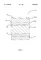
- FIG. 1is a cross-sectional illustration of a photovoltaic device made according to the method of the present invention.
- photovoltaic cell 10is structurally supported on glass substrate 16 having a thickness of one to four millimeters thick.
- Back contact metal layer 12having a thickness of approximately 1.0 micron of molybdenum is deposited on substrate 16.
- First active region 14 of device 10comprises a semiconductor layer 14 which, in the preferred embodiment, is comprised primarily of p-type copper indium diselenide having a thickness of about 3 microns.
- a thin doped copper indium gallium diselenide n-type region 18is generated by thermal diffusion with zinc chloride.
- the second active region 20 of device 10is a zinc oxide semiconductor layer having a thickness of about 0.5 microns.
- Zinc oxide layer 20is deposited in two distinct layers comprising a first high resistivity zinc oxide region 20(a) and a second low resistivity zinc oxide layer 20(b).
- Layer 20(a)has a thickness of about 0.5 microns zinc oxide while layer 20(b) is about 0.20-0.45 microns in thickness.
- High resistivity layer 20(a)comprises essentially of pure zinc oxide while layer 20(b) is doped to achieve low resistivity through any one of the well known methods.
- Device 10is completed with a grid of front face contacts 22 in the form of narrow metal strips, such as silver or aluminum, typically deposited either by sputtering, evaporation, or plating.
- the copper indium diselenide layer 14may be deposited according to the process of the above-referenced Mickelsen et al patent. However, specific examples of the fabrication of the copper indium diselenide layer 14 are also described in the Weiting and Pollock references above which are incorporated herein by reference. While references herein are to a copper indium diselenide semiconductor layer various other materials may be alloyed with this layer for various purposes. For example, aluminum, gallium, tellurium, or sulfur are well known inclusions in copper indium diselenide films to adjust band gaps, and such alloyed materials are considered equivalent to copper indium diselenide for the purposes of this invention. Likewise, as in Pollock, the precise ratios of copper, indium and selenium may be adjusted to improve the qualities of the final layer, for example, in attempts to eliminate pure copper nodules.
- a copper indium selenium filmwas prepared using a conventional three stage process. Indium and selenide having a low gallium concentration are heated to 550° C. in a selenium atmosphere with the evaporation of copper.
- the copper/indium plus gallium ratiowas 0.85-0.9.
- a device with standard window layerswas fabricated on one half of the CIGS film and the other half was used to test the following zinc chloride thermal diffusion process of the invention.
- a solution of zinc chloride in methanolwas prepared by dissolving 1 gram of zinc chloride in 100 milliliters of methanol. A few drops of the zinc chloride methanol solution was dispersed on one-half of the CIGS thin film using a dropper. The use of a zinc chloride solution as the doping source rather than solid zinc chloride was chosen for proof of concept demonstration. The methanol solvent was allowed to evaporate, leaving behind a zinc chloride layer on the surface of the CIGS film. Samples of the CIGS film having a zinc chloride layer were heated in an oven 10-60 minutes, ambient atmospheric air, at 200° C. in order to thermally diffuse zinc chloride into the surface region of the CIGS film.
- doping the upper copper indium diselenide region substrate 16 having layer 12 and region 14 to generate n-type region 18, of FIG. 1may be accomplished either by using a solid zinc chloride vapor source in a sublimation type process, or through CVD of a zinc chloride solution, preferably a 1% zinc chloride in methanol (Wt./Vol.), carried into an evacuated reactor with an inert carrier gas, such as argon.
- a vapor transport sublimation reactionof any one of the well known methods using solid zinc chloride as the vapor source in order to manufacture the devices herein in a dry inline process.
Landscapes
- Photovoltaic Devices (AREA)
Abstract
Description
Claims (11)
Priority Applications (3)
| Application Number | Priority Date | Filing Date | Title |
|---|---|---|---|
| US08/939,844US5948176A (en) | 1997-09-29 | 1997-09-29 | Cadmium-free junction fabrication process for CuInSe2 thin film solar cells |
| AU94987/98AAU9498798A (en) | 1997-09-29 | 1998-09-18 | Cadmium-free junction fabrication process for CuInSe2 thin film olarcells |
| PCT/US1998/019728WO1999017377A1 (en) | 1997-09-29 | 1998-09-18 | CADMIUM-FREE JUNCTION FABRICATION PROCESS FOR CuInSe2 THIN FILM SOLAR CELLS |
Applications Claiming Priority (1)
| Application Number | Priority Date | Filing Date | Title |
|---|---|---|---|
| US08/939,844US5948176A (en) | 1997-09-29 | 1997-09-29 | Cadmium-free junction fabrication process for CuInSe2 thin film solar cells |
Publications (1)
| Publication Number | Publication Date |
|---|---|
| US5948176Atrue US5948176A (en) | 1999-09-07 |
Family
ID=25473835
Family Applications (1)
| Application Number | Title | Priority Date | Filing Date |
|---|---|---|---|
| US08/939,844Expired - LifetimeUS5948176A (en) | 1997-09-29 | 1997-09-29 | Cadmium-free junction fabrication process for CuInSe2 thin film solar cells |
Country Status (3)
| Country | Link |
|---|---|
| US (1) | US5948176A (en) |
| AU (1) | AU9498798A (en) |
| WO (1) | WO1999017377A1 (en) |
Cited By (64)
| Publication number | Priority date | Publication date | Assignee | Title |
|---|---|---|---|---|
| US6107562A (en)* | 1998-03-24 | 2000-08-22 | Matsushita Electric Industrial Co., Ltd. | Semiconductor thin film, method for manufacturing the same, and solar cell using the same |
| US6259016B1 (en)* | 1999-03-05 | 2001-07-10 | Matsushita Electric Industrial Co., Ltd. | Solar cell |
| US6534704B2 (en) | 2000-10-18 | 2003-03-18 | Matsushita Electric Industrial Co., Ltd. | Solar cell |
| US20040261841A1 (en)* | 2003-06-26 | 2004-12-30 | Matsushita Electric Industrial Co., Ltd. | Solar cell |
| US20050151131A1 (en)* | 2002-06-11 | 2005-07-14 | Wager John F.Iii | Polycrystalline thin-film solar cells |
| US20070160770A1 (en)* | 2006-01-12 | 2007-07-12 | Stanbery Billy J | Apparatus for making controlled segregated phase domain structures |
| US20070160763A1 (en)* | 2006-01-12 | 2007-07-12 | Stanbery Billy J | Methods of making controlled segregated phase domain structures |
| US20070295396A1 (en)* | 2004-01-13 | 2007-12-27 | Matsushita Electric Industrial Co., Ltd., | Solar Cell And Production Thereof |
| EP1938964A1 (en) | 2006-12-29 | 2008-07-02 | E.I. Du Pont De Nemours And Company | Intrusion resistant safety glazings and solar cell modules |
| US20080217610A1 (en)* | 2007-03-09 | 2008-09-11 | Electronics & Telecommunications Research Institute | Thin film transistor having n-type and p-type cis thin films and method of manufacturing the same |
| US20080280119A1 (en)* | 2007-02-26 | 2008-11-13 | Murata Manufacturing Co., Ltd. | Conductive film and method for manufacturing the same |
| US20080311028A1 (en)* | 2007-06-18 | 2008-12-18 | Stanbery Billy J | Assemblies of anisotropic nanoparticles |
| US20090191359A1 (en)* | 2004-04-02 | 2009-07-30 | Bhattacharya Raghu N | ZnS/Zn(O,OH) S-based buffer layer deposition for solar cells |
| US20090242030A1 (en)* | 2008-03-26 | 2009-10-01 | E. I. Du Pont De Nemours And Company | High performance anti-spall laminate article |
| US20090250100A1 (en)* | 2008-04-04 | 2009-10-08 | E.I. Du Pont De Nemours And Company | Solar cell modules comprising high melt flow poly(vinyl butyral) encapsulants |
| US20090288701A1 (en)* | 2008-05-23 | 2009-11-26 | E.I.Du Pont De Nemours And Company | Solar cell laminates having colored multi-layer encapsulant sheets |
| US20100101647A1 (en)* | 2008-10-24 | 2010-04-29 | E.I. Du Pont De Nemours And Company | Non-autoclave lamination process for manufacturing solar cell modules |
| US20100129665A1 (en)* | 2008-11-24 | 2010-05-27 | E.I. Du Pont De Nemours And Company | Laminated articles comprising a sheet of a blend of ethylene copolymers |
| US20100154867A1 (en)* | 2008-12-19 | 2010-06-24 | E. I. Du Pont De Nemours And Company | Mechanically reliable solar cell modules |
| US20100163099A1 (en)* | 2008-12-31 | 2010-07-01 | E. I. Du Pont De Nemours And Company | Solar cell modules comprising encapsulant sheets with low haze and high moisture resistance |
| US20100180943A1 (en)* | 2009-01-22 | 2010-07-22 | E. I. Du Pont De Nemours And Company | Poly(vinyl butyral) encapsulant comprising chelating agents for solar cell modules |
| US20100233841A1 (en)* | 2003-05-08 | 2010-09-16 | Solibro Research Ab | Thin-film solar cell |
| US20100258180A1 (en)* | 2009-02-04 | 2010-10-14 | Yuepeng Deng | Method of forming an indium-containing transparent conductive oxide film, metal targets used in the method and photovoltaic devices utilizing said films |
| US20100258167A1 (en)* | 2009-04-10 | 2010-10-14 | Pvnext Corporation | Photovoltaic cell structure and manufacturing method |
| US20100310770A1 (en)* | 2009-06-05 | 2010-12-09 | Baosheng Sang | Process for synthesizing a thin film or composition layer via non-contact pressure containment |
| US20110018103A1 (en)* | 2008-10-02 | 2011-01-27 | Stion Corporation | System and method for transferring substrates in large scale processing of cigs and/or cis devices |
| US20110023943A1 (en)* | 2009-07-31 | 2011-02-03 | E. I. Du Pont De Nemours And Company | Cross-linkable encapsulants for photovoltaic cells |
| WO2011028269A1 (en)* | 2009-09-04 | 2011-03-10 | Heliovolt Corporation | Cadmium-free thin film for use in solar cells |
| US20110062049A1 (en)* | 2009-09-11 | 2011-03-17 | Pro-Pak Industries, Inc. | Load tray and method for unitizing a palletized load |
| US20110168243A1 (en)* | 2010-01-14 | 2011-07-14 | Elowe Paul R | Moisture resistant photovoltaic devices with exposed conductive grid |
| US20110189080A1 (en)* | 2010-02-04 | 2011-08-04 | Curtis Calvin J | Methods of making copper selenium precursor compositions with a targeted copper selenide content and precursor compositions and thin films resulting therefrom |
| US20110192453A1 (en)* | 2010-02-09 | 2011-08-11 | Degroot Marty W | Moisture resistant photovoltaic devices with improved adhesion of barrier film |
| US20110203634A1 (en)* | 2010-01-22 | 2011-08-25 | Stion Corporation | Method and Structure for Tiling Industrial Thin-Film Solar Devices |
| US20110230006A1 (en)* | 2010-03-29 | 2011-09-22 | Stion Corporation | Large Scale MOCVD System for Thin Film Photovoltaic Devices |
| US8080727B2 (en) | 2008-11-24 | 2011-12-20 | E. I. Du Pont De Nemours And Company | Solar cell modules comprising an encapsulant sheet of a blend of ethylene copolymers |
| DE202007019352U1 (en) | 2006-08-30 | 2012-01-31 | E.I. Du Pont De Nemours And Company | Solar cell modules comprising poly (allylamine) and poly (vinylamine) primed polyester films |
| WO2012016053A1 (en) | 2010-07-30 | 2012-02-02 | E. I. Du Pont De Nemours And Company | Cross-linkable ionomeric encapsulants for photovoltaic cells |
| US8241943B1 (en) | 2009-05-08 | 2012-08-14 | Stion Corporation | Sodium doping method and system for shaped CIGS/CIS based thin film solar cells |
| US20120240989A1 (en)* | 2010-10-01 | 2012-09-27 | Stion Corporation | Method and Device for Cadmium-Free Solar Cells |
| US20120285523A1 (en)* | 2010-01-21 | 2012-11-15 | Takayuki Negami | Solar cell |
| US8372684B1 (en) | 2009-05-14 | 2013-02-12 | Stion Corporation | Method and system for selenization in fabricating CIGS/CIS solar cells |
| US8399095B2 (en) | 2008-10-31 | 2013-03-19 | E I Du Pont De Nemours And Company | Solar cells modules comprising low haze encapsulants |
| US8398772B1 (en) | 2009-08-18 | 2013-03-19 | Stion Corporation | Method and structure for processing thin film PV cells with improved temperature uniformity |
| US8404512B1 (en)* | 2011-03-04 | 2013-03-26 | Solopower, Inc. | Crystallization methods for preparing group IBIIIAVIA thin film solar absorbers |
| US8445776B2 (en) | 2008-06-02 | 2013-05-21 | E I Du Pont De Nemours And Company | Solar cell module having a low haze encapsulant layer |
| US8461061B2 (en) | 2010-07-23 | 2013-06-11 | Stion Corporation | Quartz boat method and apparatus for thin film thermal treatment |
| US8507786B1 (en) | 2009-06-27 | 2013-08-13 | Stion Corporation | Manufacturing method for patterning CIGS/CIS solar cells |
| US20130298980A1 (en)* | 2012-05-10 | 2013-11-14 | International Business Machines Corporation | Cone-shaped holes for high efficiency thin film solar cells |
| US8673675B2 (en) | 2008-09-30 | 2014-03-18 | Stion Corporation | Humidity control and method for thin film photovoltaic materials |
| US8741689B2 (en)* | 2008-10-01 | 2014-06-03 | Stion Corporation | Thermal pre-treatment process for soda lime glass substrate for thin film photovoltaic materials |
| WO2014100301A1 (en) | 2012-12-19 | 2014-06-26 | E. I. Du Pont De Nemours And Company | Cross-linked polymers and their use in photovoltaic modules |
| CN104011872A (en)* | 2011-10-20 | 2014-08-27 | Lg伊诺特有限公司 | Solar cell and manufacturing method thereof |
| US20140308774A1 (en)* | 2010-10-01 | 2014-10-16 | Stion Corporation | Method and device for cadmium-free solar cells |
| US8871305B2 (en) | 2007-06-29 | 2014-10-28 | Stion Corporation | Methods for infusing one or more materials into nano-voids of nanoporous or nanostructured materials |
| WO2014188386A1 (en)* | 2013-05-24 | 2014-11-27 | Commissariat A L'energie Atomique Et Aux Energies Alternatives | Method for producing the p-n junction of a thin-film photovoltaic cell and corresponding method for producing a photovoltaic cell |
| EP2782143A4 (en)* | 2011-11-16 | 2015-06-17 | Toshiba Kk | PHOTOELECTRIC CONVERSION ELEMENT AND PHOTOPILE |
| US9096930B2 (en) | 2010-03-29 | 2015-08-04 | Stion Corporation | Apparatus for manufacturing thin film photovoltaic devices |
| US9105797B2 (en) | 2012-05-31 | 2015-08-11 | Alliance For Sustainable Energy, Llc | Liquid precursor inks for deposition of In—Se, Ga—Se and In—Ga—Se |
| CN104885205A (en)* | 2012-06-20 | 2015-09-02 | 法国圣戈班玻璃厂 | Layer system for thin-film solar cells |
| US9130084B2 (en) | 2010-05-21 | 2015-09-08 | Alliance for Substainable Energy, LLC | Liquid precursor for deposition of copper selenide and method of preparing the same |
| US9142408B2 (en) | 2010-08-16 | 2015-09-22 | Alliance For Sustainable Energy, Llc | Liquid precursor for deposition of indium selenide and method of preparing the same |
| WO2015171575A1 (en) | 2014-05-09 | 2015-11-12 | E. I. Du Pont De Nemours And Company | Encapsulant composition comprising a copolymer of ethylene, vinyl acetate and a third comonomer |
| TWI514611B (en)* | 2013-03-26 | 2015-12-21 | Canon Anelva Corp | A solar cell manufacturing method, and a solar cell |
| WO2019173262A1 (en) | 2018-03-08 | 2019-09-12 | E. I. Du Pont De Nemours And Company | Photovoltaic module and encapsulant composition having improved resistance to potential induced degradation |
Families Citing this family (3)
| Publication number | Priority date | Publication date | Assignee | Title |
|---|---|---|---|---|
| AU2003300775A1 (en)* | 2003-09-03 | 2005-04-21 | Midwest Research Institute | Zno/cu(inga)se2 solar cells prepared by vapor phase zn doping |
| CN102859720A (en)* | 2010-04-27 | 2013-01-02 | 京瓷株式会社 | Photoelectric conversion element, photoelectric conversion device, and method for manufacturing photoelectric conversion element |
| JP5697581B2 (en)* | 2011-11-16 | 2015-04-08 | 株式会社東芝 | Photoelectric conversion element and solar cell |
Citations (6)
| Publication number | Priority date | Publication date | Assignee | Title |
|---|---|---|---|---|
| US4242374A (en)* | 1979-04-19 | 1980-12-30 | Exxon Research & Engineering Co. | Process for thin film deposition of metal and mixed metal chalcogenides displaying semi-conductor properties |
| US4327119A (en)* | 1981-02-03 | 1982-04-27 | Radiation Monitoring Devices, Inc. | Method to synthesize and produce thin films by spray pyrolysis |
| US4612411A (en)* | 1985-06-04 | 1986-09-16 | Atlantic Richfield Company | Thin film solar cell with ZnO window layer |
| US4751149A (en)* | 1985-06-04 | 1988-06-14 | Atlantic Richfield Company | Chemical vapor deposition of zinc oxide films and products |
| US4950615A (en)* | 1989-02-06 | 1990-08-21 | International Solar Electric Technology, Inc. | Method and making group IIB metal - telluride films and solar cells |
| US5474939A (en)* | 1992-12-30 | 1995-12-12 | Siemens Solar Industries International | Method of making thin film heterojunction solar cell |
- 1997
- 1997-09-29USUS08/939,844patent/US5948176A/ennot_activeExpired - Lifetime
- 1998
- 1998-09-18WOPCT/US1998/019728patent/WO1999017377A1/enactiveApplication Filing
- 1998-09-18AUAU94987/98Apatent/AU9498798A/ennot_activeAbandoned
Patent Citations (6)
| Publication number | Priority date | Publication date | Assignee | Title |
|---|---|---|---|---|
| US4242374A (en)* | 1979-04-19 | 1980-12-30 | Exxon Research & Engineering Co. | Process for thin film deposition of metal and mixed metal chalcogenides displaying semi-conductor properties |
| US4327119A (en)* | 1981-02-03 | 1982-04-27 | Radiation Monitoring Devices, Inc. | Method to synthesize and produce thin films by spray pyrolysis |
| US4612411A (en)* | 1985-06-04 | 1986-09-16 | Atlantic Richfield Company | Thin film solar cell with ZnO window layer |
| US4751149A (en)* | 1985-06-04 | 1988-06-14 | Atlantic Richfield Company | Chemical vapor deposition of zinc oxide films and products |
| US4950615A (en)* | 1989-02-06 | 1990-08-21 | International Solar Electric Technology, Inc. | Method and making group IIB metal - telluride films and solar cells |
| US5474939A (en)* | 1992-12-30 | 1995-12-12 | Siemens Solar Industries International | Method of making thin film heterojunction solar cell |
Non-Patent Citations (4)
| Title |
|---|
| Aranovich, Optical and Electrical Properties of ZnO Films Prepared by Spray Pyrolysis for Solar Cell Applications, J. Vac. Sci. Technol., vol. 16, No. 4, pp. 994 1007, Jul. 1979.* |
| Aranovich, Optical and Electrical Properties of ZnO Films Prepared by Spray Pyrolysis for Solar Cell Applications, J. Vac. Sci. Technol., vol. 16, No. 4, pp. 994-1007, Jul. 1979. |
| Tomar, A ZnO/p CuInSe2 Thin Film Solar Cell Prepared Entirely by Spray Pyrolysis, Thin Solid Films, 90, pp. 419 423, 1982.* |
| Tomar, A ZnO/p-CuInSe2 Thin Film Solar Cell Prepared Entirely by Spray Pyrolysis, Thin Solid Films, 90, pp. 419-423, 1982. |
Cited By (98)
| Publication number | Priority date | Publication date | Assignee | Title |
|---|---|---|---|---|
| US6107562A (en)* | 1998-03-24 | 2000-08-22 | Matsushita Electric Industrial Co., Ltd. | Semiconductor thin film, method for manufacturing the same, and solar cell using the same |
| US6259016B1 (en)* | 1999-03-05 | 2001-07-10 | Matsushita Electric Industrial Co., Ltd. | Solar cell |
| US6534704B2 (en) | 2000-10-18 | 2003-03-18 | Matsushita Electric Industrial Co., Ltd. | Solar cell |
| US20050151131A1 (en)* | 2002-06-11 | 2005-07-14 | Wager John F.Iii | Polycrystalline thin-film solar cells |
| US20100233841A1 (en)* | 2003-05-08 | 2010-09-16 | Solibro Research Ab | Thin-film solar cell |
| US8865512B2 (en) | 2003-05-08 | 2014-10-21 | Solibro Research Ab | Thin-film solar cell |
| US20040261841A1 (en)* | 2003-06-26 | 2004-12-30 | Matsushita Electric Industrial Co., Ltd. | Solar cell |
| EP1705717A4 (en)* | 2004-01-13 | 2009-04-08 | Panasonic Corp | FUEL CELL AND PROCESS FOR PRODUCING THE SAME |
| US20070295396A1 (en)* | 2004-01-13 | 2007-12-27 | Matsushita Electric Industrial Co., Ltd., | Solar Cell And Production Thereof |
| US7557294B2 (en) | 2004-01-13 | 2009-07-07 | Panasonic Corporation | Solar cell and production thereof |
| US20090191359A1 (en)* | 2004-04-02 | 2009-07-30 | Bhattacharya Raghu N | ZnS/Zn(O,OH) S-based buffer layer deposition for solar cells |
| US7611573B2 (en) | 2004-04-02 | 2009-11-03 | Alliance For Sustainable Energy, Llc | ZnS/Zn(O,OH)S-based buffer layer deposition for solar cells |
| US20070160763A1 (en)* | 2006-01-12 | 2007-07-12 | Stanbery Billy J | Methods of making controlled segregated phase domain structures |
| US8084685B2 (en) | 2006-01-12 | 2011-12-27 | Heliovolt Corporation | Apparatus for making controlled segregated phase domain structures |
| US20070160770A1 (en)* | 2006-01-12 | 2007-07-12 | Stanbery Billy J | Apparatus for making controlled segregated phase domain structures |
| DE202007019352U1 (en) | 2006-08-30 | 2012-01-31 | E.I. Du Pont De Nemours And Company | Solar cell modules comprising poly (allylamine) and poly (vinylamine) primed polyester films |
| EP1938964A1 (en) | 2006-12-29 | 2008-07-02 | E.I. Du Pont De Nemours And Company | Intrusion resistant safety glazings and solar cell modules |
| DE202007019226U1 (en) | 2006-12-29 | 2011-04-14 | E.I. Du Pont De Nemours And Company, Wilmington | Penetration-resistant safety glazing and solar cell modules |
| EP2286994A1 (en) | 2006-12-29 | 2011-02-23 | E. I. du Pont de Nemours and Company | Intrusion resistant safety glazings and solar cell modules |
| EP2061041A4 (en)* | 2007-02-26 | 2011-06-29 | Murata Manufacturing Co | CONDUCTIVE FILM AND METHOD FOR PRODUCING CONDUCTIVE FILM |
| US20080280119A1 (en)* | 2007-02-26 | 2008-11-13 | Murata Manufacturing Co., Ltd. | Conductive film and method for manufacturing the same |
| US20080217610A1 (en)* | 2007-03-09 | 2008-09-11 | Electronics & Telecommunications Research Institute | Thin film transistor having n-type and p-type cis thin films and method of manufacturing the same |
| US20110045633A1 (en)* | 2007-03-09 | 2011-02-24 | Electronics And Telecommunications Research Institute | Thin film transistor having n-type and p-type cis thin films and method of manufacturing the same |
| US8084295B2 (en) | 2007-03-09 | 2011-12-27 | Electronics And Telecommunications Research Institute | Thin film transistor having n-type and p-type CIS thin films and method of manufacturing the same |
| US7851791B2 (en) | 2007-03-09 | 2010-12-14 | Electronics And Telecommunications Research Institute | Thin film transistor having N-type and P-type CIS thin films and method of manufacturing the same |
| US20080311028A1 (en)* | 2007-06-18 | 2008-12-18 | Stanbery Billy J | Assemblies of anisotropic nanoparticles |
| US8034317B2 (en) | 2007-06-18 | 2011-10-11 | Heliovolt Corporation | Assemblies of anisotropic nanoparticles |
| US7939048B2 (en) | 2007-06-18 | 2011-05-10 | Heliovolt Corporation | Assemblies of anisotropic nanoparticles |
| US8871305B2 (en) | 2007-06-29 | 2014-10-28 | Stion Corporation | Methods for infusing one or more materials into nano-voids of nanoporous or nanostructured materials |
| US20090242030A1 (en)* | 2008-03-26 | 2009-10-01 | E. I. Du Pont De Nemours And Company | High performance anti-spall laminate article |
| US20090250100A1 (en)* | 2008-04-04 | 2009-10-08 | E.I. Du Pont De Nemours And Company | Solar cell modules comprising high melt flow poly(vinyl butyral) encapsulants |
| US20090288701A1 (en)* | 2008-05-23 | 2009-11-26 | E.I.Du Pont De Nemours And Company | Solar cell laminates having colored multi-layer encapsulant sheets |
| US8445776B2 (en) | 2008-06-02 | 2013-05-21 | E I Du Pont De Nemours And Company | Solar cell module having a low haze encapsulant layer |
| US8673675B2 (en) | 2008-09-30 | 2014-03-18 | Stion Corporation | Humidity control and method for thin film photovoltaic materials |
| US8741689B2 (en)* | 2008-10-01 | 2014-06-03 | Stion Corporation | Thermal pre-treatment process for soda lime glass substrate for thin film photovoltaic materials |
| US20110018103A1 (en)* | 2008-10-02 | 2011-01-27 | Stion Corporation | System and method for transferring substrates in large scale processing of cigs and/or cis devices |
| US20100101647A1 (en)* | 2008-10-24 | 2010-04-29 | E.I. Du Pont De Nemours And Company | Non-autoclave lamination process for manufacturing solar cell modules |
| US8399095B2 (en) | 2008-10-31 | 2013-03-19 | E I Du Pont De Nemours And Company | Solar cells modules comprising low haze encapsulants |
| US8084129B2 (en) | 2008-11-24 | 2011-12-27 | E. I. Du Pont De Nemours And Company | Laminated articles comprising a sheet of a blend of ethylene copolymers |
| US20100129665A1 (en)* | 2008-11-24 | 2010-05-27 | E.I. Du Pont De Nemours And Company | Laminated articles comprising a sheet of a blend of ethylene copolymers |
| US8080727B2 (en) | 2008-11-24 | 2011-12-20 | E. I. Du Pont De Nemours And Company | Solar cell modules comprising an encapsulant sheet of a blend of ethylene copolymers |
| WO2010080469A2 (en) | 2008-12-19 | 2010-07-15 | E. I. Du Pont De Nemours And Company | Mechanically reliable solar cell modules |
| US20100154867A1 (en)* | 2008-12-19 | 2010-06-24 | E. I. Du Pont De Nemours And Company | Mechanically reliable solar cell modules |
| US20100163099A1 (en)* | 2008-12-31 | 2010-07-01 | E. I. Du Pont De Nemours And Company | Solar cell modules comprising encapsulant sheets with low haze and high moisture resistance |
| US8399081B2 (en) | 2008-12-31 | 2013-03-19 | E I Du Pont De Nemours And Company | Solar cell modules comprising encapsulant sheets with low haze and high moisture resistance |
| US20100180943A1 (en)* | 2009-01-22 | 2010-07-22 | E. I. Du Pont De Nemours And Company | Poly(vinyl butyral) encapsulant comprising chelating agents for solar cell modules |
| US8338699B2 (en) | 2009-01-22 | 2012-12-25 | E I Du Pont De Nemours And Company | Poly(vinyl butyral) encapsulant comprising chelating agents for solar cell modules |
| US20100258180A1 (en)* | 2009-02-04 | 2010-10-14 | Yuepeng Deng | Method of forming an indium-containing transparent conductive oxide film, metal targets used in the method and photovoltaic devices utilizing said films |
| US20100258167A1 (en)* | 2009-04-10 | 2010-10-14 | Pvnext Corporation | Photovoltaic cell structure and manufacturing method |
| US8241943B1 (en) | 2009-05-08 | 2012-08-14 | Stion Corporation | Sodium doping method and system for shaped CIGS/CIS based thin film solar cells |
| US8372684B1 (en) | 2009-05-14 | 2013-02-12 | Stion Corporation | Method and system for selenization in fabricating CIGS/CIS solar cells |
| US20100310770A1 (en)* | 2009-06-05 | 2010-12-09 | Baosheng Sang | Process for synthesizing a thin film or composition layer via non-contact pressure containment |
| US8507786B1 (en) | 2009-06-27 | 2013-08-13 | Stion Corporation | Manufacturing method for patterning CIGS/CIS solar cells |
| US20110023943A1 (en)* | 2009-07-31 | 2011-02-03 | E. I. Du Pont De Nemours And Company | Cross-linkable encapsulants for photovoltaic cells |
| US8609777B2 (en) | 2009-07-31 | 2013-12-17 | E I Du Pont De Nemours And Company | Cross-linkable encapsulants for photovoltaic cells |
| US8398772B1 (en) | 2009-08-18 | 2013-03-19 | Stion Corporation | Method and structure for processing thin film PV cells with improved temperature uniformity |
| WO2011028269A1 (en)* | 2009-09-04 | 2011-03-10 | Heliovolt Corporation | Cadmium-free thin film for use in solar cells |
| US20110062049A1 (en)* | 2009-09-11 | 2011-03-17 | Pro-Pak Industries, Inc. | Load tray and method for unitizing a palletized load |
| US20110168243A1 (en)* | 2010-01-14 | 2011-07-14 | Elowe Paul R | Moisture resistant photovoltaic devices with exposed conductive grid |
| US8921148B2 (en) | 2010-01-14 | 2014-12-30 | Dow Global Technologies Llc | Moisture resistant photovoltaic devices with exposed conductive grid |
| US20120285523A1 (en)* | 2010-01-21 | 2012-11-15 | Takayuki Negami | Solar cell |
| US8859880B2 (en) | 2010-01-22 | 2014-10-14 | Stion Corporation | Method and structure for tiling industrial thin-film solar devices |
| US20110203634A1 (en)* | 2010-01-22 | 2011-08-25 | Stion Corporation | Method and Structure for Tiling Industrial Thin-Film Solar Devices |
| US20110189080A1 (en)* | 2010-02-04 | 2011-08-04 | Curtis Calvin J | Methods of making copper selenium precursor compositions with a targeted copper selenide content and precursor compositions and thin films resulting therefrom |
| US8021641B2 (en) | 2010-02-04 | 2011-09-20 | Alliance For Sustainable Energy, Llc | Methods of making copper selenium precursor compositions with a targeted copper selenide content and precursor compositions and thin films resulting therefrom |
| US9059349B2 (en)* | 2010-02-09 | 2015-06-16 | Dow Global Technologies Llc | Moisture resistant photovoltaic devices with improved adhesion of barrier film |
| US20110192453A1 (en)* | 2010-02-09 | 2011-08-11 | Degroot Marty W | Moisture resistant photovoltaic devices with improved adhesion of barrier film |
| US20110230006A1 (en)* | 2010-03-29 | 2011-09-22 | Stion Corporation | Large Scale MOCVD System for Thin Film Photovoltaic Devices |
| US9096930B2 (en) | 2010-03-29 | 2015-08-04 | Stion Corporation | Apparatus for manufacturing thin film photovoltaic devices |
| US8142521B2 (en) | 2010-03-29 | 2012-03-27 | Stion Corporation | Large scale MOCVD system for thin film photovoltaic devices |
| US9130084B2 (en) | 2010-05-21 | 2015-09-08 | Alliance for Substainable Energy, LLC | Liquid precursor for deposition of copper selenide and method of preparing the same |
| US8461061B2 (en) | 2010-07-23 | 2013-06-11 | Stion Corporation | Quartz boat method and apparatus for thin film thermal treatment |
| US8609980B2 (en) | 2010-07-30 | 2013-12-17 | E I Du Pont De Nemours And Company | Cross-linkable ionomeric encapsulants for photovoltaic cells |
| WO2012016053A1 (en) | 2010-07-30 | 2012-02-02 | E. I. Du Pont De Nemours And Company | Cross-linkable ionomeric encapsulants for photovoltaic cells |
| US9142408B2 (en) | 2010-08-16 | 2015-09-22 | Alliance For Sustainable Energy, Llc | Liquid precursor for deposition of indium selenide and method of preparing the same |
| US20120240989A1 (en)* | 2010-10-01 | 2012-09-27 | Stion Corporation | Method and Device for Cadmium-Free Solar Cells |
| US8906732B2 (en)* | 2010-10-01 | 2014-12-09 | Stion Corporation | Method and device for cadmium-free solar cells |
| US20140308774A1 (en)* | 2010-10-01 | 2014-10-16 | Stion Corporation | Method and device for cadmium-free solar cells |
| US20150136231A1 (en)* | 2010-10-01 | 2015-05-21 | Stion Corporation | Method and device for cadmium-free solar cells |
| US8628997B2 (en)* | 2010-10-01 | 2014-01-14 | Stion Corporation | Method and device for cadmium-free solar cells |
| US8404512B1 (en)* | 2011-03-04 | 2013-03-26 | Solopower, Inc. | Crystallization methods for preparing group IBIIIAVIA thin film solar absorbers |
| CN104011872A (en)* | 2011-10-20 | 2014-08-27 | Lg伊诺特有限公司 | Solar cell and manufacturing method thereof |
| US9935229B2 (en)* | 2011-10-20 | 2018-04-03 | Lg Innotek Co., Ltd. | Solar cell and method of fabricating the same |
| US20150053267A1 (en)* | 2011-10-20 | 2015-02-26 | Lg Innotek Co., Ltd. | Solar cell and method of fabricating the same |
| EP2782143A4 (en)* | 2011-11-16 | 2015-06-17 | Toshiba Kk | PHOTOELECTRIC CONVERSION ELEMENT AND PHOTOPILE |
| US20130298980A1 (en)* | 2012-05-10 | 2013-11-14 | International Business Machines Corporation | Cone-shaped holes for high efficiency thin film solar cells |
| US9876129B2 (en)* | 2012-05-10 | 2018-01-23 | International Business Machines Corporation | Cone-shaped holes for high efficiency thin film solar cells |
| US9105797B2 (en) | 2012-05-31 | 2015-08-11 | Alliance For Sustainable Energy, Llc | Liquid precursor inks for deposition of In—Se, Ga—Se and In—Ga—Se |
| JP2015528200A (en)* | 2012-06-20 | 2015-09-24 | サン−ゴバン グラス フランスSaint−Gobain Glass France | Layers for thin film solar cells |
| CN104885205A (en)* | 2012-06-20 | 2015-09-02 | 法国圣戈班玻璃厂 | Layer system for thin-film solar cells |
| CN104885205B (en)* | 2012-06-20 | 2017-06-20 | 法国圣戈班玻璃厂 | The layer system of thin-layer solar cell |
| WO2014100301A1 (en) | 2012-12-19 | 2014-06-26 | E. I. Du Pont De Nemours And Company | Cross-linked polymers and their use in photovoltaic modules |
| TWI514611B (en)* | 2013-03-26 | 2015-12-21 | Canon Anelva Corp | A solar cell manufacturing method, and a solar cell |
| US9640687B2 (en) | 2013-05-24 | 2017-05-02 | Commissariat A L'energie Atomique Et Aux Energies Alternatives | Method for producing the P-N junction of a thin-film photovoltaic cell and corresponding method for producing a photovoltaic cell |
| FR3006109A1 (en)* | 2013-05-24 | 2014-11-28 | Commissariat Energie Atomique | METHOD OF MAKING THE P-N JUNCTION OF A THIN FILM PHOTOVOLTAIC CELL AND METHOD OF OBTAINING THE PHOTOVOLTAIC CELL |
| WO2014188386A1 (en)* | 2013-05-24 | 2014-11-27 | Commissariat A L'energie Atomique Et Aux Energies Alternatives | Method for producing the p-n junction of a thin-film photovoltaic cell and corresponding method for producing a photovoltaic cell |
| WO2015171575A1 (en) | 2014-05-09 | 2015-11-12 | E. I. Du Pont De Nemours And Company | Encapsulant composition comprising a copolymer of ethylene, vinyl acetate and a third comonomer |
| WO2019173262A1 (en) | 2018-03-08 | 2019-09-12 | E. I. Du Pont De Nemours And Company | Photovoltaic module and encapsulant composition having improved resistance to potential induced degradation |
Also Published As
| Publication number | Publication date |
|---|---|
| WO1999017377A1 (en) | 1999-04-08 |
| AU9498798A (en) | 1999-04-23 |
Similar Documents
| Publication | Publication Date | Title |
|---|---|---|
| US5948176A (en) | Cadmium-free junction fabrication process for CuInSe2 thin film solar cells | |
| US4612411A (en) | Thin film solar cell with ZnO window layer | |
| Compaan et al. | High efficiency, magnetron sputtered CdS/CdTe solar cells | |
| US4094704A (en) | Dual electrically insulated solar cells | |
| US5078804A (en) | I-III-VI2 based solar cell utilizing the structure CuInGaSe2 CdZnS/ZnO | |
| KR101503557B1 (en) | Photovoltaic devices including an interfacial layer | |
| US6137048A (en) | Process for fabricating polycrystalline semiconductor thin-film solar cells, and cells produced thereby | |
| US8512528B2 (en) | Method and system for large scale manufacture of thin film photovoltaic devices using single-chamber configuration | |
| EP1492169A2 (en) | Solar cell | |
| AU2010257207B2 (en) | Cadmium telluride thin film photovoltaic devices and methods of manufacturing the same | |
| WO2006016577A1 (en) | Cis type compound semiconductor thin film solar cell and method for preparing light-absorbing layer of said solar cell | |
| JP2922466B2 (en) | Thin film solar cell | |
| US4342879A (en) | Thin film photovoltaic device | |
| GB2405030A (en) | Bifacial thin film solar cell | |
| US20140000703A1 (en) | Thin Film Article and Method for Forming a Reduced Conductive Area in Transparent Conductive Films for Photovoltaic Modules | |
| CN102237418B (en) | The cadmium sulfide layer used based on the film photovoltaic device of cadmium telluride and manufacture method thereof | |
| US20120322198A1 (en) | METHODS FOR SUBLIMATION OF Mg AND INCORPORATION INTO CdTe FILMS TO FORM TERNARY COMPOSITIONS | |
| JP3468328B2 (en) | Manufacturing method of semiconductor thin film | |
| JP3061342B2 (en) | Method for manufacturing transparent conductive film and photoelectric conversion semiconductor device | |
| JP2003008039A (en) | Method for manufacturing compound solar cell | |
| Basol et al. | Preparation of Cd (Zn) Te and CuInSe2 films and devices by a two-stage process | |
| KR102596328B1 (en) | Preparation method for CZTS thin film solar cell absorbing layer, CZTS thin film solar cell absorbing layer prepared therefrom | |
| KR102212042B1 (en) | Solar cell comprising buffer layer formed by atomic layer deposition and method of fabricating the same | |
| KR101485009B1 (en) | fabricating method of CIGS base thin film solar cell and solar cell thereof | |
| JPH09213978A (en) | Semiconductor of chalcopyrite structure and photovolatic device therewith |
Legal Events
| Date | Code | Title | Description |
|---|---|---|---|
| AS | Assignment | Owner name:MIDWEST RESEARCH INSTITUTE, MISSOURI Free format text:ASSIGNMENT OF ASSIGNORS INTEREST;ASSIGNORS:RAMANATHAN, KANNAN V.;CONTRERAS, MIGUEL A.;BHATTACHARYA, RAGHU N.;AND OTHERS;REEL/FRAME:008974/0235;SIGNING DATES FROM 19980203 TO 19980205 | |
| STCF | Information on status: patent grant | Free format text:PATENTED CASE | |
| CC | Certificate of correction | ||
| FEPP | Fee payment procedure | Free format text:PAT HOLDER CLAIMS SMALL ENTITY STATUS, ENTITY STATUS SET TO SMALL (ORIGINAL EVENT CODE: LTOS); ENTITY STATUS OF PATENT OWNER: LARGE ENTITY | |
| FPAY | Fee payment | Year of fee payment:4 | |
| REMI | Maintenance fee reminder mailed | ||
| AS | Assignment | Owner name:U.S. DEPARTMENT OF ENERGY, DISTRICT OF COLUMBIA Free format text:CONFIRMATORY LICENSE;ASSIGNOR:MIDWEST RESEARCH INSTITUTE;REEL/FRAME:016153/0262 Effective date:19980206 | |
| FPAY | Fee payment | Year of fee payment:8 | |
| AS | Assignment | Owner name:ALLIANCE FOR SUSTAINABLE ENERGY, LLC, COLORADO Free format text:ASSIGNMENT OF ASSIGNORS INTEREST;ASSIGNOR:MIDWEST RESEARCH INSTITUTE;REEL/FRAME:021603/0337 Effective date:20080912 Owner name:ALLIANCE FOR SUSTAINABLE ENERGY, LLC,COLORADO Free format text:ASSIGNMENT OF ASSIGNORS INTEREST;ASSIGNOR:MIDWEST RESEARCH INSTITUTE;REEL/FRAME:021603/0337 Effective date:20080912 | |
| FPAY | Fee payment | Year of fee payment:12 | |
| SULP | Surcharge for late payment |