US5946588A - Low temperature sub-atmospheric ozone oxidation process for making thin gate oxides - Google Patents
Low temperature sub-atmospheric ozone oxidation process for making thin gate oxidesDownload PDFInfo
- Publication number
- US5946588A US5946588AUS08/779,602US77960297AUS5946588AUS 5946588 AUS5946588 AUS 5946588AUS 77960297 AUS77960297 AUS 77960297AUS 5946588 AUS5946588 AUS 5946588A
- Authority
- US
- United States
- Prior art keywords
- ozone
- oxide
- oxide layer
- substrate
- torr
- Prior art date
- Legal status (The legal status is an assumption and is not a legal conclusion. Google has not performed a legal analysis and makes no representation as to the accuracy of the status listed.)
- Expired - Lifetime
Links
Images

Classifications
- H—ELECTRICITY
- H01—ELECTRIC ELEMENTS
- H01L—SEMICONDUCTOR DEVICES NOT COVERED BY CLASS H10
- H01L21/00—Processes or apparatus adapted for the manufacture or treatment of semiconductor or solid state devices or of parts thereof
- H01L21/02—Manufacture or treatment of semiconductor devices or of parts thereof
- H01L21/04—Manufacture or treatment of semiconductor devices or of parts thereof the devices having potential barriers, e.g. a PN junction, depletion layer or carrier concentration layer
- H01L21/18—Manufacture or treatment of semiconductor devices or of parts thereof the devices having potential barriers, e.g. a PN junction, depletion layer or carrier concentration layer the devices having semiconductor bodies comprising elements of Group IV of the Periodic Table or AIIIBV compounds with or without impurities, e.g. doping materials
- H01L21/28—Manufacture of electrodes on semiconductor bodies using processes or apparatus not provided for in groups H01L21/20 - H01L21/268
- H01L21/28008—Making conductor-insulator-semiconductor electrodes
- H01L21/28017—Making conductor-insulator-semiconductor electrodes the insulator being formed after the semiconductor body, the semiconductor being silicon
- H01L21/28158—Making the insulator
- H01L21/28167—Making the insulator on single crystalline silicon, e.g. using a liquid, i.e. chemical oxidation
- H01L21/28211—Making the insulator on single crystalline silicon, e.g. using a liquid, i.e. chemical oxidation in a gaseous ambient using an oxygen or a water vapour, e.g. RTO, possibly through a layer
- H—ELECTRICITY
- H01—ELECTRIC ELEMENTS
- H01L—SEMICONDUCTOR DEVICES NOT COVERED BY CLASS H10
- H01L21/00—Processes or apparatus adapted for the manufacture or treatment of semiconductor or solid state devices or of parts thereof
- H01L21/70—Manufacture or treatment of devices consisting of a plurality of solid state components formed in or on a common substrate or of parts thereof; Manufacture of integrated circuit devices or of parts thereof
- H01L21/71—Manufacture of specific parts of devices defined in group H01L21/70
- H01L21/76—Making of isolation regions between components
- H01L21/762—Dielectric regions, e.g. EPIC dielectric isolation, LOCOS; Trench refilling techniques, SOI technology, use of channel stoppers
- H01L21/76202—Dielectric regions, e.g. EPIC dielectric isolation, LOCOS; Trench refilling techniques, SOI technology, use of channel stoppers using a local oxidation of silicon, e.g. LOCOS, SWAMI, SILO
- H01L21/76213—Dielectric regions, e.g. EPIC dielectric isolation, LOCOS; Trench refilling techniques, SOI technology, use of channel stoppers using a local oxidation of silicon, e.g. LOCOS, SWAMI, SILO introducing electrical inactive or active impurities in the local oxidation region, e.g. to alter LOCOS oxide growth characteristics or for additional isolation purpose
- H01L21/76216—Dielectric regions, e.g. EPIC dielectric isolation, LOCOS; Trench refilling techniques, SOI technology, use of channel stoppers using a local oxidation of silicon, e.g. LOCOS, SWAMI, SILO introducing electrical inactive or active impurities in the local oxidation region, e.g. to alter LOCOS oxide growth characteristics or for additional isolation purpose introducing electrical active impurities in the local oxidation region for the sole purpose of creating channel stoppers
- H—ELECTRICITY
- H01—ELECTRIC ELEMENTS
- H01L—SEMICONDUCTOR DEVICES NOT COVERED BY CLASS H10
- H01L21/00—Processes or apparatus adapted for the manufacture or treatment of semiconductor or solid state devices or of parts thereof
- H01L21/02—Manufacture or treatment of semiconductor devices or of parts thereof
- H01L21/02104—Forming layers
- H01L21/02107—Forming insulating materials on a substrate
- H01L21/02225—Forming insulating materials on a substrate characterised by the process for the formation of the insulating layer
- H01L21/02227—Forming insulating materials on a substrate characterised by the process for the formation of the insulating layer formation by a process other than a deposition process
- H01L21/0223—Forming insulating materials on a substrate characterised by the process for the formation of the insulating layer formation by a process other than a deposition process formation by oxidation, e.g. oxidation of the substrate
- H01L21/02233—Forming insulating materials on a substrate characterised by the process for the formation of the insulating layer formation by a process other than a deposition process formation by oxidation, e.g. oxidation of the substrate of the semiconductor substrate or a semiconductor layer
- H01L21/02236—Forming insulating materials on a substrate characterised by the process for the formation of the insulating layer formation by a process other than a deposition process formation by oxidation, e.g. oxidation of the substrate of the semiconductor substrate or a semiconductor layer group IV semiconductor
- H01L21/02238—Forming insulating materials on a substrate characterised by the process for the formation of the insulating layer formation by a process other than a deposition process formation by oxidation, e.g. oxidation of the substrate of the semiconductor substrate or a semiconductor layer group IV semiconductor silicon in uncombined form, i.e. pure silicon
- H—ELECTRICITY
- H01—ELECTRIC ELEMENTS
- H01L—SEMICONDUCTOR DEVICES NOT COVERED BY CLASS H10
- H01L21/00—Processes or apparatus adapted for the manufacture or treatment of semiconductor or solid state devices or of parts thereof
- H01L21/02—Manufacture or treatment of semiconductor devices or of parts thereof
- H01L21/02104—Forming layers
- H01L21/02107—Forming insulating materials on a substrate
- H01L21/02225—Forming insulating materials on a substrate characterised by the process for the formation of the insulating layer
- H01L21/02227—Forming insulating materials on a substrate characterised by the process for the formation of the insulating layer formation by a process other than a deposition process
- H01L21/02255—Forming insulating materials on a substrate characterised by the process for the formation of the insulating layer formation by a process other than a deposition process formation by thermal treatment
Definitions
- This inventionrelates to semiconductor manufacturing, and more particularly to forming thin gate oxides.
- the process of the present inventionuses ozone oxidation to grow thin gate oxide useful for deep sub-half micron devices where a shallow channel implant is necessary to maintain the required surface concentration of dopant at the silicon surface.
- Applicantsare able to grow an ozone gate oxide to a thickness of 110 ⁇ or less.
- the low temperature gate oxidation process of the present inventionrequires less of an enhancement dose of dopant (which is typically implanted prior to gate oxide growth through the sacrificial oxide).
- the reduced enhancement dopingis very much needed for P-channel devices in order to control Yj (the junction depth of the channel implant or enhancement in a P-channel buried channel process), and thereby maintain short channel characteristics.
- Yjthe junction depth of the channel implant or enhancement in a P-channel buried channel process
- the reduced enhancement dopingprovides the optimum surface concentration for the N-channel MOSFETs without effecting the N+ sidewall junctions.
- One aspect of the present inventionis a low temperature oxidation process for fabricating thin oxide layers comprising growing a gate oxide in an ozone-containing atmosphere, which atmosphere is generated at a temperature substantially in the range of 600° C. to 957° C.
- Another aspect of the present inventionis a process for making thin gate oxides comprising the layering of a semiconductor substrate with at least an oxide layer and a nitride layer.
- the layersare then patterned and etched, thereby exposing portions of the substrate.
- the exposed portions of the substrateare oxidized, thereby creating a field oxide region.
- the substrateis then doped, thereby creating a channel stop region.
- the oxide and nitride layersare removed, thereby exposing sites of active areas, and a gate oxide layer grown in an ozone-containing atmosphere.
- a further aspect of the present inventionis a method of fabricating thin dielectric layers comprising growing a field oxide region in a semiconductor substrate, doping the semiconductor substrate to form channel stop regions, and growing a thin oxide layer having a thickness 110 ⁇ or less in an ozone-containing atmosphere at approximately 700° C.
- FIG. 1is a schematic cross-section of a semiconductor substrate which has been masked and doped, according to the process of the present invention
- FIG. 2is a schematic cross-section of the substrate of FIG. 1, after a field oxide region has been grown, according to the process of the present invention
- FIG. 3is a schematic cross-section of the substrate of FIG. 2, on which has been formed a gate oxide and layer of polysilicon, according to the process of the present invention
- FIG. 4is a schematic cross-section of the substrate of FIG. 3, after the gate devices have been formed, according to the process of the present invention.
- FIG. 5is a graph indicating the Concentration vs. Distance on the dopant in the N-well and P-well.
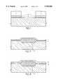
- FIG. 1illustrates the standard LOCOS process, in which a pad oxide layer 2 is formed upon a semiconductor substrate 1.
- the pad layer 2is created either by thermal growth or by deposition.
- Superjacent the pad oxide 2is formed a silicon nitride layer 3 which functions as an oxidation barrier.
- the nitride layer 3is typically deposited by chemical vapor deposition (CVD).
- a mask 4is patterned superjacent the sites where the active areas will be formed.
- the silicon nitride layer 3 and pad oxide layer 2are etched, thereby exposing the semiconductor substrate 1.
- the semiconductor substrate 1is then exposed to a steam ambient and the field oxide 5 is grown.
- the field oxidation stepis preferably done before the channel stop region is formed, so that the diffusion of the boron is minimized due to the oxidation in a steam ambient.
- the field oxide region 5is then doped to form channel stop regions 6.
- Low temperature oxidationcauses less boron diffusion into the substrate 1, thus allowing higher concentrations under the field oxide 5.
- the diffusion of boron speciesis a strong function of temperature; the diffusion being lower at lower temperatures.
- a higher concentrationserves the purposes of lessening the dose for the channel stop implant that gives a better field oxide threshold voltage, and also lessens the junction leakage at the field oxide 5 edges due to less electrical encroachment, thereby improving the refresh in the DRAM.
- the field oxide region 5is grown by oxidizing the exposed substrate 1 in an ozone-containing ambient. See, for example, U.S. patent application Ser. No. 08/181,650, entitled, "Improved Process for Creating Silicon Dioxide Field Isolation Regions on a Silicon Substrate Using Ozone Chemistries,” also assigned to Micron Semiconductor, Inc.
- the mask 4, the silicon nitride layer 3, and the pad oxide layer 2are stripped off, and a sacrificial oxide layer 7 is grown and then stripped away, as illustrated in FIG. 2.
- the sacrificial oxide 7is used to remove any nitride impurities that have impacted the substrate 1.
- a thin gate oxide layer 8is then formed.
- the thin gate oxide 8 of the present inventionhas a thickness of 110 ⁇ or less.
- a polysilicon layer 9is disposed superjacent the gate oxide layer 8, and transistors are created at the active area sites.
- the thin gate oxide 8is formed using ozone oxidation at low temperatures.
- the ozone gate processesare run at temperatures in the approximate range of 600° C. to 960° C.
- the preferred temperature rangeis 750° C. to 910° C.
- Oxidation in the presence of ozonedramatically increases the oxidation rate over dry oxidation.
- the faster oxidation ratespermit the use of the lower oxidation temperatures, which in turn, result in less stress, reduced electrical encroachment, and a reduced amount of enhancement dose of dopant.
- the reduced enhancement dopingis very much needed to maintain short channel characteristics.
- Each wafermay be processed individually in a single wafer processor, or multiple wafers may be processed in a conventional vertical thermal reactor.
- Applicantsused a Silicon Valley Group (SVG) vertical furnace having a gas flow rate of 5 standard liters/minute at a pressure of 350 torr.
- the composition of the gaswas 5% O 3 in bulk O 2 . It is contemplated that the oxidation rate will increase further with increased levels of ozone concentration.
- the reactoris a standard, low pressure vertical furnace system configured to run at sub-atmospheric pressures (e.g. at least 1 Torr) when creating the oxide film 8.
- sub-atmospheric pressurese.g. at least 1 Torr
- other single wafer radially heated systemssuch as rapid thermal processors, laser heated in plasma assisted CVD systems can also be used.
- the systemexhibits depletion of reactants similar to other Low Pressure Chemical Vapor Deposition (LPCVD) processes (e.g., polysilicon and nitride depositions).
- LPCVDLow Pressure Chemical Vapor Deposition
- This depletion of reactantsis not typical of oxidation processes.
- the depletion of reactantsis attributed to the depletion of the ozone reactants.
- the depletionrequires a non-uniform temperature control across the reactor load to achieve similar effective oxidation rates. This is also typical of other LPCVD processes.
- Ozone concentrationshave been run at known conditions as high as 10%, with 7% being a previous "standard,” due to limitations of a then-existing ozone generator. A new generators which should allow experimentation up to a possible 20% are not available. It is believed even greater results will be achievable with such a generator.
- the use of a small amount of nitrogen with the generatorhas affected the oxidation rate, even at 25 sccm N 2 in a 5 standard liters/minute of ozone/O 2 .
- the nitrogenis used to increase the efficiency of the ozone generator, and its effective lifetime.
- the ozoneincreases the effective oxidation rate of silicon, compared to dry oxygen alone.
- the increase in oxidation rateappears to be a function of ozone concentration as well, with a higher ozone concentration causing a greater increase in oxidation rate compared to dry oxygen.
- the effect of the nitrogen in the ozone/O 2 reactant flow with the new generatoris expected to have comparable results to those of the standard generators.
- Ozone oxidation in a rapid thermal processoralso produces thin gate films.
- the advantage in that caseis the immediate ability for in-situ nitridization using N 2 O/NO and re-oxidation to build a stacked dielectric, with superior film thickness uniformity compared to the furnace process.
- the re-oxidationfills the pinholes, and thereby avoids excess leakage, which improves the cell dielectric reliability, and consequently, the refresh time of the memory cell, such as a DRAM.
- In-situ precleanscan be done prior to oxidation, as well as to engineer the properties of the gate dielectric.
- the low thermal budget provided by the low temperature oxidation (i.e., 600° C.-950° C.) of the present inventionis useful for reducing the overall thermal budget in sub-half micron densities.
- Recent characterization of the ozone gate oxide film 8 grown at approximately 900° C.shows the film 8 has at least comparable breakdown voltage mean and distributions compared to dry oxides and dry/wet/dry oxides grown at 800° C. At 750° C., the ozone gate oxide thickness of 90 ⁇ or less is also comparable. This is advantageous in that the lower temperature gate dielectrics have inferior breakdown and lifetime characteristics, when not annealed, as proposed by the present invention.
- the refractive index of the 750° C. ozone oxideindicates that it is not a poor quality oxide, i.e., neither excessively silicon nor excessively oxygen rich.
- the extra oxygen species introduced which enhance oxidation and which have higher diffusivity through the gate oxide film 8 during oxidationprevents a silicon-rich film from forming.
- the greater diffusivity and reactivity of these speciesprovide a better film uniformity than a DCS/N 2 O (dichlorosilane/nitrous oxide) process for depositing a gate dielectric with higher quality.
- FIG. 5illustrates the buried channel in an N-well formation due to a boron enhancement implant, the channel adjustment implant is portrayed by curve D.
- Curves B and Ccharacterize the dopant density versus depth of respective P- and N-wells of a substrate.
- Curve Aillustrates the density versus depth of dopants for a buried channel PMOSFET. The more shallow the buried channel, the better the short channel characteristics of the PMOSFET achieved.
- One purpose of the process of the present inventionis to make the buried channel shallow by allowing less thermal cycle during gate oxidation.
Landscapes
- Engineering & Computer Science (AREA)
- Microelectronics & Electronic Packaging (AREA)
- Condensed Matter Physics & Semiconductors (AREA)
- General Physics & Mathematics (AREA)
- Manufacturing & Machinery (AREA)
- Computer Hardware Design (AREA)
- Physics & Mathematics (AREA)
- Power Engineering (AREA)
- Chemical & Material Sciences (AREA)
- Chemical Kinetics & Catalysis (AREA)
- Crystallography & Structural Chemistry (AREA)
- General Chemical & Material Sciences (AREA)
- Formation Of Insulating Films (AREA)
- Insulated Gate Type Field-Effect Transistor (AREA)
Abstract
Description
Claims (12)
Priority Applications (1)
| Application Number | Priority Date | Filing Date | Title |
|---|---|---|---|
| US08/779,602US5946588A (en) | 1994-12-07 | 1997-01-07 | Low temperature sub-atmospheric ozone oxidation process for making thin gate oxides |
Applications Claiming Priority (2)
| Application Number | Priority Date | Filing Date | Title |
|---|---|---|---|
| US35085994A | 1994-12-07 | 1994-12-07 | |
| US08/779,602US5946588A (en) | 1994-12-07 | 1997-01-07 | Low temperature sub-atmospheric ozone oxidation process for making thin gate oxides |
Related Parent Applications (1)
| Application Number | Title | Priority Date | Filing Date |
|---|---|---|---|
| US35085994AContinuation | 1994-12-07 | 1994-12-07 |
Publications (1)
| Publication Number | Publication Date |
|---|---|
| US5946588Atrue US5946588A (en) | 1999-08-31 |
Family
ID=23378503
Family Applications (1)
| Application Number | Title | Priority Date | Filing Date |
|---|---|---|---|
| US08/779,602Expired - LifetimeUS5946588A (en) | 1994-12-07 | 1997-01-07 | Low temperature sub-atmospheric ozone oxidation process for making thin gate oxides |
Country Status (1)
| Country | Link |
|---|---|
| US (1) | US5946588A (en) |
Cited By (7)
| Publication number | Priority date | Publication date | Assignee | Title |
|---|---|---|---|---|
| US6172383B1 (en) | 1997-12-31 | 2001-01-09 | Siliconix Incorporated | Power MOSFET having voltage-clamped gate |
| US6268242B1 (en)* | 1997-12-31 | 2001-07-31 | Richard K. Williams | Method of forming vertical mosfet device having voltage clamped gate and self-aligned contact |
| US20020102859A1 (en)* | 2001-01-31 | 2002-08-01 | Yoo Woo Sik | Method for ultra thin film formation |
| US6511921B1 (en)* | 1999-01-12 | 2003-01-28 | Sumco Phoenix Corporation | Methods for reducing the reactivity of a semiconductor substrate surface and for evaluating electrical properties of a semiconductor substrate |
| US6667197B1 (en) | 2002-12-06 | 2003-12-23 | International Business Machines Corporation | Method for differential oxidation rate reduction for n-type and p-type materials |
| US6900111B2 (en)* | 2001-07-04 | 2005-05-31 | Advanced Micro Devices, Inc. | Method of forming a thin oxide layer having improved reliability on a semiconductor surface |
| US20080044574A1 (en)* | 2006-08-21 | 2008-02-21 | Macronix International Co., Ltd. | Method of manufacturing nano-crystalline silicon dot layer |
Citations (4)
| Publication number | Priority date | Publication date | Assignee | Title |
|---|---|---|---|---|
| JPH05175190A (en)* | 1991-12-24 | 1993-07-13 | Sharp Corp | Manufacture of semiconductor device |
| US5294571A (en)* | 1992-07-22 | 1994-03-15 | Vlsi Technology, Inc. | Rapid thermal oxidation of silicon in an ozone ambient |
| US5330935A (en)* | 1990-10-24 | 1994-07-19 | International Business Machines Corporation | Low temperature plasma oxidation process |
| US5352620A (en)* | 1984-05-23 | 1994-10-04 | Hitachi, Ltd. | Method of making semiconductor device with memory cells and peripheral transistors |
- 1997
- 1997-01-07USUS08/779,602patent/US5946588A/ennot_activeExpired - Lifetime
Patent Citations (4)
| Publication number | Priority date | Publication date | Assignee | Title |
|---|---|---|---|---|
| US5352620A (en)* | 1984-05-23 | 1994-10-04 | Hitachi, Ltd. | Method of making semiconductor device with memory cells and peripheral transistors |
| US5330935A (en)* | 1990-10-24 | 1994-07-19 | International Business Machines Corporation | Low temperature plasma oxidation process |
| JPH05175190A (en)* | 1991-12-24 | 1993-07-13 | Sharp Corp | Manufacture of semiconductor device |
| US5294571A (en)* | 1992-07-22 | 1994-03-15 | Vlsi Technology, Inc. | Rapid thermal oxidation of silicon in an ozone ambient |
Non-Patent Citations (6)
| Title |
|---|
| Kazor, A., et al, "Growth Rate Enhancement Using Ozone . . . Silicon", Appl. Phys. Lett. 65(4), Jul. 25, 1994, pp. 412-414. |
| Kazor, A., et al, "Ozone Induced Rapid Low Temperature Oxidation of Silicon", Appl. Phys. Lett., 63(18) Nov. 1, 1993 pp. 2517-2519. |
| Kazor, A., et al, Growth Rate Enhancement Using Ozone . . . Silicon , Appl. Phys. Lett. 65(4), Jul. 25, 1994, pp. 412 414.* |
| Kazor, A., et al, Ozone Induced Rapid Low Temperature Oxidation of Silicon , Appl. Phys. Lett., 63(18) Nov. 1, 1993 pp. 2517 2519.* |
| Nayan et al, "Atmospheric Pressure, Low Temperature (500°) UV/ozone Oxidation of Silicon", Elect. Lett. Feb., 1,1990, Oct. 26, No. 3, pp. 205-206. |
| Nayan et al, Atmospheric Pressure, Low Temperature (500 ) UV/ozone Oxidation of Silicon , Elect. Lett. Feb., 1,1990, Oct. 26, No. 3, pp. 205 206.* |
Cited By (9)
| Publication number | Priority date | Publication date | Assignee | Title |
|---|---|---|---|---|
| US6172383B1 (en) | 1997-12-31 | 2001-01-09 | Siliconix Incorporated | Power MOSFET having voltage-clamped gate |
| US6268242B1 (en)* | 1997-12-31 | 2001-07-31 | Richard K. Williams | Method of forming vertical mosfet device having voltage clamped gate and self-aligned contact |
| US6511921B1 (en)* | 1999-01-12 | 2003-01-28 | Sumco Phoenix Corporation | Methods for reducing the reactivity of a semiconductor substrate surface and for evaluating electrical properties of a semiconductor substrate |
| US20020102859A1 (en)* | 2001-01-31 | 2002-08-01 | Yoo Woo Sik | Method for ultra thin film formation |
| WO2002061819A3 (en)* | 2001-01-31 | 2003-11-06 | Wafermasters Inc | Method for ultra thin film formation |
| US6900111B2 (en)* | 2001-07-04 | 2005-05-31 | Advanced Micro Devices, Inc. | Method of forming a thin oxide layer having improved reliability on a semiconductor surface |
| US6667197B1 (en) | 2002-12-06 | 2003-12-23 | International Business Machines Corporation | Method for differential oxidation rate reduction for n-type and p-type materials |
| US20080044574A1 (en)* | 2006-08-21 | 2008-02-21 | Macronix International Co., Ltd. | Method of manufacturing nano-crystalline silicon dot layer |
| US7927660B2 (en)* | 2006-08-21 | 2011-04-19 | Macronix International Co., Ltd. | Method of manufacturing nano-crystalline silicon dot layer |
Similar Documents
| Publication | Publication Date | Title |
|---|---|---|
| KR0122513B1 (en) | Method of Oxidizing Silicon Nitride in Semiconductor Devices | |
| US5998289A (en) | Process for obtaining a transistor having a silicon-germanium gate | |
| US6033998A (en) | Method of forming variable thickness gate dielectrics | |
| US5580815A (en) | Process for forming field isolation and a structure over a semiconductor substrate | |
| EP0617461B1 (en) | Oxynitride dielectric process for IC manufacture | |
| US4692992A (en) | Method of forming isolation regions in a semiconductor device | |
| EP0428283B1 (en) | Method for local oxidation of silicon | |
| US6069041A (en) | Process for manufacturing non-volatile semiconductor memory device by introducing nitrogen atoms | |
| US6368927B1 (en) | Method of manufacturing transistor having elevated source and drain regions | |
| US5661335A (en) | Semicondutor having selectively enhanced field oxide areas and method for producing same | |
| US6376318B1 (en) | Method of manufacturing a semiconductor device | |
| US20060289902A1 (en) | Method for forming raised structures by controlled selective epitaxial growth of facet using spacer | |
| US6413881B1 (en) | Process for forming thin gate oxide with enhanced reliability by nitridation of upper surface of gate of oxide to form barrier of nitrogen atoms in upper surface region of gate oxide, and resulting product | |
| US7514337B2 (en) | Semiconductor device using EPI-layer and method of forming the same | |
| US7183166B2 (en) | Method for forming oxide on ONO structure | |
| KR100550196B1 (en) | How to improve gate activation by employing atomic oxygen oxidation | |
| US5672539A (en) | Method for forming an improved field isolation structure using ozone enhanced oxidation and tapering | |
| JP2002198526A (en) | Method for manufacturing semiconductor device | |
| KR100718823B1 (en) | A silicon-germanium transistor and associated methods | |
| US5946588A (en) | Low temperature sub-atmospheric ozone oxidation process for making thin gate oxides | |
| US5219783A (en) | Method of making semiconductor well structure | |
| US6248618B1 (en) | Method of fabrication of dual gate oxides for CMOS devices | |
| EP0110103B1 (en) | Method of making complementary transistor metal oxide semiconductor structures | |
| US6753232B2 (en) | Method for fabricating semiconductor device | |
| US4409726A (en) | Method of making well regions for CMOS devices |
Legal Events
| Date | Code | Title | Description |
|---|---|---|---|
| STCF | Information on status: patent grant | Free format text:PATENTED CASE | |
| FPAY | Fee payment | Year of fee payment:4 | |
| FPAY | Fee payment | Year of fee payment:8 | |
| FPAY | Fee payment | Year of fee payment:12 | |
| AS | Assignment | Owner name:U.S. BANK NATIONAL ASSOCIATION, AS COLLATERAL AGENT, CALIFORNIA Free format text:SECURITY INTEREST;ASSIGNOR:MICRON TECHNOLOGY, INC.;REEL/FRAME:038669/0001 Effective date:20160426 Owner name:U.S. BANK NATIONAL ASSOCIATION, AS COLLATERAL AGEN Free format text:SECURITY INTEREST;ASSIGNOR:MICRON TECHNOLOGY, INC.;REEL/FRAME:038669/0001 Effective date:20160426 | |
| AS | Assignment | Owner name:MORGAN STANLEY SENIOR FUNDING, INC., AS COLLATERAL AGENT, MARYLAND Free format text:PATENT SECURITY AGREEMENT;ASSIGNOR:MICRON TECHNOLOGY, INC.;REEL/FRAME:038954/0001 Effective date:20160426 Owner name:MORGAN STANLEY SENIOR FUNDING, INC., AS COLLATERAL Free format text:PATENT SECURITY AGREEMENT;ASSIGNOR:MICRON TECHNOLOGY, INC.;REEL/FRAME:038954/0001 Effective date:20160426 | |
| AS | Assignment | Owner name:U.S. BANK NATIONAL ASSOCIATION, AS COLLATERAL AGENT, CALIFORNIA Free format text:CORRECTIVE ASSIGNMENT TO CORRECT THE REPLACE ERRONEOUSLY FILED PATENT #7358718 WITH THE CORRECT PATENT #7358178 PREVIOUSLY RECORDED ON REEL 038669 FRAME 0001. ASSIGNOR(S) HEREBY CONFIRMS THE SECURITY INTEREST;ASSIGNOR:MICRON TECHNOLOGY, INC.;REEL/FRAME:043079/0001 Effective date:20160426 Owner name:U.S. BANK NATIONAL ASSOCIATION, AS COLLATERAL AGEN Free format text:CORRECTIVE ASSIGNMENT TO CORRECT THE REPLACE ERRONEOUSLY FILED PATENT #7358718 WITH THE CORRECT PATENT #7358178 PREVIOUSLY RECORDED ON REEL 038669 FRAME 0001. ASSIGNOR(S) HEREBY CONFIRMS THE SECURITY INTEREST;ASSIGNOR:MICRON TECHNOLOGY, INC.;REEL/FRAME:043079/0001 Effective date:20160426 | |
| AS | Assignment | Owner name:MICRON TECHNOLOGY, INC., IDAHO Free format text:RELEASE BY SECURED PARTY;ASSIGNOR:U.S. BANK NATIONAL ASSOCIATION, AS COLLATERAL AGENT;REEL/FRAME:047243/0001 Effective date:20180629 | |
| AS | Assignment | Owner name:MICRON TECHNOLOGY, INC., IDAHO Free format text:RELEASE BY SECURED PARTY;ASSIGNOR:MORGAN STANLEY SENIOR FUNDING, INC., AS COLLATERAL AGENT;REEL/FRAME:050937/0001 Effective date:20190731 |