US5946559A - Membrane dielectric isolation IC fabrication - Google Patents
Membrane dielectric isolation IC fabricationDownload PDFInfo
- Publication number
- US5946559A US5946559AUS08/472,426US47242695AUS5946559AUS 5946559 AUS5946559 AUS 5946559AUS 47242695 AUS47242695 AUS 47242695AUS 5946559 AUS5946559 AUS 5946559A
- Authority
- US
- United States
- Prior art keywords
- membrane
- layer
- semiconductor
- substrate
- dielectric
- Prior art date
- Legal status (The legal status is an assumption and is not a legal conclusion. Google has not performed a legal analysis and makes no representation as to the accuracy of the status listed.)
- Expired - Lifetime
Links
Images


Classifications
- H—ELECTRICITY
- H01—ELECTRIC ELEMENTS
- H01L—SEMICONDUCTOR DEVICES NOT COVERED BY CLASS H10
- H01L25/00—Assemblies consisting of a plurality of semiconductor or other solid state devices
- H01L25/50—Multistep manufacturing processes of assemblies consisting of devices, the devices being individual devices of subclass H10D or integrated devices of class H10
- H—ELECTRICITY
- H01—ELECTRIC ELEMENTS
- H01L—SEMICONDUCTOR DEVICES NOT COVERED BY CLASS H10
- H01L21/00—Processes or apparatus adapted for the manufacture or treatment of semiconductor or solid state devices or of parts thereof
- G—PHYSICS
- G03—PHOTOGRAPHY; CINEMATOGRAPHY; ANALOGOUS TECHNIQUES USING WAVES OTHER THAN OPTICAL WAVES; ELECTROGRAPHY; HOLOGRAPHY
- G03F—PHOTOMECHANICAL PRODUCTION OF TEXTURED OR PATTERNED SURFACES, e.g. FOR PRINTING, FOR PROCESSING OF SEMICONDUCTOR DEVICES; MATERIALS THEREFOR; ORIGINALS THEREFOR; APPARATUS SPECIALLY ADAPTED THEREFOR
- G03F7/00—Photomechanical, e.g. photolithographic, production of textured or patterned surfaces, e.g. printing surfaces; Materials therefor, e.g. comprising photoresists; Apparatus specially adapted therefor
- G03F7/70—Microphotolithographic exposure; Apparatus therefor
- G03F7/70483—Information management; Active and passive control; Testing; Wafer monitoring, e.g. pattern monitoring
- G03F7/70605—Workpiece metrology
- G03F7/70653—Metrology techniques
- G03F7/70658—Electrical testing
- G—PHYSICS
- G11—INFORMATION STORAGE
- G11C—STATIC STORES
- G11C29/00—Checking stores for correct operation ; Subsequent repair; Testing stores during standby or offline operation
- G11C29/006—Checking stores for correct operation ; Subsequent repair; Testing stores during standby or offline operation at wafer scale level, i.e. wafer scale integration [WSI]
- H—ELECTRICITY
- H01—ELECTRIC ELEMENTS
- H01L—SEMICONDUCTOR DEVICES NOT COVERED BY CLASS H10
- H01L21/00—Processes or apparatus adapted for the manufacture or treatment of semiconductor or solid state devices or of parts thereof
- H01L21/70—Manufacture or treatment of devices consisting of a plurality of solid state components formed in or on a common substrate or of parts thereof; Manufacture of integrated circuit devices or of parts thereof
- H01L21/71—Manufacture of specific parts of devices defined in group H01L21/70
- H01L21/76—Making of isolation regions between components
- H01L21/762—Dielectric regions, e.g. EPIC dielectric isolation, LOCOS; Trench refilling techniques, SOI technology, use of channel stoppers
- H01L21/7624—Dielectric regions, e.g. EPIC dielectric isolation, LOCOS; Trench refilling techniques, SOI technology, use of channel stoppers using semiconductor on insulator [SOI] technology
- H01L21/76264—SOI together with lateral isolation, e.g. using local oxidation of silicon, or dielectric or polycristalline material refilled trench or air gap isolation regions, e.g. completely isolated semiconductor islands
- H—ELECTRICITY
- H01—ELECTRIC ELEMENTS
- H01L—SEMICONDUCTOR DEVICES NOT COVERED BY CLASS H10
- H01L21/00—Processes or apparatus adapted for the manufacture or treatment of semiconductor or solid state devices or of parts thereof
- H01L21/70—Manufacture or treatment of devices consisting of a plurality of solid state components formed in or on a common substrate or of parts thereof; Manufacture of integrated circuit devices or of parts thereof
- H01L21/71—Manufacture of specific parts of devices defined in group H01L21/70
- H01L21/76—Making of isolation regions between components
- H01L21/764—Air gaps
- H—ELECTRICITY
- H01—ELECTRIC ELEMENTS
- H01L—SEMICONDUCTOR DEVICES NOT COVERED BY CLASS H10
- H01L23/00—Details of semiconductor or other solid state devices
- H01L23/52—Arrangements for conducting electric current within the device in operation from one component to another, i.e. interconnections, e.g. wires, lead frames
- H01L23/538—Arrangements for conducting electric current within the device in operation from one component to another, i.e. interconnections, e.g. wires, lead frames the interconnection structure between a plurality of semiconductor chips being formed on, or in, insulating substrates
- H01L23/5381—Crossover interconnections, e.g. bridge stepovers
- H—ELECTRICITY
- H01—ELECTRIC ELEMENTS
- H01L—SEMICONDUCTOR DEVICES NOT COVERED BY CLASS H10
- H01L23/00—Details of semiconductor or other solid state devices
- H01L23/52—Arrangements for conducting electric current within the device in operation from one component to another, i.e. interconnections, e.g. wires, lead frames
- H01L23/538—Arrangements for conducting electric current within the device in operation from one component to another, i.e. interconnections, e.g. wires, lead frames the interconnection structure between a plurality of semiconductor chips being formed on, or in, insulating substrates
- H01L23/5383—Multilayer substrates
- H—ELECTRICITY
- H01—ELECTRIC ELEMENTS
- H01L—SEMICONDUCTOR DEVICES NOT COVERED BY CLASS H10
- H01L23/00—Details of semiconductor or other solid state devices
- H01L23/52—Arrangements for conducting electric current within the device in operation from one component to another, i.e. interconnections, e.g. wires, lead frames
- H01L23/538—Arrangements for conducting electric current within the device in operation from one component to another, i.e. interconnections, e.g. wires, lead frames the interconnection structure between a plurality of semiconductor chips being formed on, or in, insulating substrates
- H01L23/5386—Geometry or layout of the interconnection structure
- H—ELECTRICITY
- H01—ELECTRIC ELEMENTS
- H01L—SEMICONDUCTOR DEVICES NOT COVERED BY CLASS H10
- H01L23/00—Details of semiconductor or other solid state devices
- H01L23/52—Arrangements for conducting electric current within the device in operation from one component to another, i.e. interconnections, e.g. wires, lead frames
- H01L23/538—Arrangements for conducting electric current within the device in operation from one component to another, i.e. interconnections, e.g. wires, lead frames the interconnection structure between a plurality of semiconductor chips being formed on, or in, insulating substrates
- H01L23/5387—Flexible insulating substrates
- H—ELECTRICITY
- H01—ELECTRIC ELEMENTS
- H01L—SEMICONDUCTOR DEVICES NOT COVERED BY CLASS H10
- H01L25/00—Assemblies consisting of a plurality of semiconductor or other solid state devices
- H01L25/03—Assemblies consisting of a plurality of semiconductor or other solid state devices all the devices being of a type provided for in a single subclass of subclasses H10B, H10D, H10F, H10H, H10K or H10N, e.g. assemblies of rectifier diodes
- H01L25/04—Assemblies consisting of a plurality of semiconductor or other solid state devices all the devices being of a type provided for in a single subclass of subclasses H10B, H10D, H10F, H10H, H10K or H10N, e.g. assemblies of rectifier diodes the devices not having separate containers
- H01L25/065—Assemblies consisting of a plurality of semiconductor or other solid state devices all the devices being of a type provided for in a single subclass of subclasses H10B, H10D, H10F, H10H, H10K or H10N, e.g. assemblies of rectifier diodes the devices not having separate containers the devices being of a type provided for in group H10D89/00
- H01L25/0652—Assemblies consisting of a plurality of semiconductor or other solid state devices all the devices being of a type provided for in a single subclass of subclasses H10B, H10D, H10F, H10H, H10K or H10N, e.g. assemblies of rectifier diodes the devices not having separate containers the devices being of a type provided for in group H10D89/00 the devices being arranged next and on each other, i.e. mixed assemblies
- H—ELECTRICITY
- H01—ELECTRIC ELEMENTS
- H01L—SEMICONDUCTOR DEVICES NOT COVERED BY CLASS H10
- H01L25/00—Assemblies consisting of a plurality of semiconductor or other solid state devices
- H01L25/03—Assemblies consisting of a plurality of semiconductor or other solid state devices all the devices being of a type provided for in a single subclass of subclasses H10B, H10D, H10F, H10H, H10K or H10N, e.g. assemblies of rectifier diodes
- H01L25/04—Assemblies consisting of a plurality of semiconductor or other solid state devices all the devices being of a type provided for in a single subclass of subclasses H10B, H10D, H10F, H10H, H10K or H10N, e.g. assemblies of rectifier diodes the devices not having separate containers
- H01L25/065—Assemblies consisting of a plurality of semiconductor or other solid state devices all the devices being of a type provided for in a single subclass of subclasses H10B, H10D, H10F, H10H, H10K or H10N, e.g. assemblies of rectifier diodes the devices not having separate containers the devices being of a type provided for in group H10D89/00
- H01L25/0655—Assemblies consisting of a plurality of semiconductor or other solid state devices all the devices being of a type provided for in a single subclass of subclasses H10B, H10D, H10F, H10H, H10K or H10N, e.g. assemblies of rectifier diodes the devices not having separate containers the devices being of a type provided for in group H10D89/00 the devices being arranged next to each other
- G—PHYSICS
- G02—OPTICS
- G02F—OPTICAL DEVICES OR ARRANGEMENTS FOR THE CONTROL OF LIGHT BY MODIFICATION OF THE OPTICAL PROPERTIES OF THE MEDIA OF THE ELEMENTS INVOLVED THEREIN; NON-LINEAR OPTICS; FREQUENCY-CHANGING OF LIGHT; OPTICAL LOGIC ELEMENTS; OPTICAL ANALOGUE/DIGITAL CONVERTERS
- G02F1/00—Devices or arrangements for the control of the intensity, colour, phase, polarisation or direction of light arriving from an independent light source, e.g. switching, gating or modulating; Non-linear optics
- G02F1/01—Devices or arrangements for the control of the intensity, colour, phase, polarisation or direction of light arriving from an independent light source, e.g. switching, gating or modulating; Non-linear optics for the control of the intensity, phase, polarisation or colour
- G02F1/13—Devices or arrangements for the control of the intensity, colour, phase, polarisation or direction of light arriving from an independent light source, e.g. switching, gating or modulating; Non-linear optics for the control of the intensity, phase, polarisation or colour based on liquid crystals, e.g. single liquid crystal display cells
- G02F1/133—Constructional arrangements; Operation of liquid crystal cells; Circuit arrangements
- G02F1/1333—Constructional arrangements; Manufacturing methods
- G02F1/1345—Conductors connecting electrodes to cell terminals
- G02F1/13452—Conductors connecting driver circuitry and terminals of panels
- G—PHYSICS
- G02—OPTICS
- G02F—OPTICAL DEVICES OR ARRANGEMENTS FOR THE CONTROL OF LIGHT BY MODIFICATION OF THE OPTICAL PROPERTIES OF THE MEDIA OF THE ELEMENTS INVOLVED THEREIN; NON-LINEAR OPTICS; FREQUENCY-CHANGING OF LIGHT; OPTICAL LOGIC ELEMENTS; OPTICAL ANALOGUE/DIGITAL CONVERTERS
- G02F1/00—Devices or arrangements for the control of the intensity, colour, phase, polarisation or direction of light arriving from an independent light source, e.g. switching, gating or modulating; Non-linear optics
- G02F1/01—Devices or arrangements for the control of the intensity, colour, phase, polarisation or direction of light arriving from an independent light source, e.g. switching, gating or modulating; Non-linear optics for the control of the intensity, phase, polarisation or colour
- G02F1/13—Devices or arrangements for the control of the intensity, colour, phase, polarisation or direction of light arriving from an independent light source, e.g. switching, gating or modulating; Non-linear optics for the control of the intensity, phase, polarisation or colour based on liquid crystals, e.g. single liquid crystal display cells
- G02F1/133—Constructional arrangements; Operation of liquid crystal cells; Circuit arrangements
- G02F1/136—Liquid crystal cells structurally associated with a semi-conducting layer or substrate, e.g. cells forming part of an integrated circuit
- G02F1/1362—Active matrix addressed cells
- G02F1/136277—Active matrix addressed cells formed on a semiconductor substrate, e.g. of silicon
- G02F1/136281—Active matrix addressed cells formed on a semiconductor substrate, e.g. of silicon having a transmissive semiconductor substrate
- H—ELECTRICITY
- H01—ELECTRIC ELEMENTS
- H01L—SEMICONDUCTOR DEVICES NOT COVERED BY CLASS H10
- H01L21/00—Processes or apparatus adapted for the manufacture or treatment of semiconductor or solid state devices or of parts thereof
- H01L21/70—Manufacture or treatment of devices consisting of a plurality of solid state components formed in or on a common substrate or of parts thereof; Manufacture of integrated circuit devices or of parts thereof
- H01L21/71—Manufacture of specific parts of devices defined in group H01L21/70
- H01L21/76—Making of isolation regions between components
- H01L21/762—Dielectric regions, e.g. EPIC dielectric isolation, LOCOS; Trench refilling techniques, SOI technology, use of channel stoppers
- H01L21/7624—Dielectric regions, e.g. EPIC dielectric isolation, LOCOS; Trench refilling techniques, SOI technology, use of channel stoppers using semiconductor on insulator [SOI] technology
- H01L21/76264—SOI together with lateral isolation, e.g. using local oxidation of silicon, or dielectric or polycristalline material refilled trench or air gap isolation regions, e.g. completely isolated semiconductor islands
- H01L21/76289—Lateral isolation by air gap
- H—ELECTRICITY
- H01—ELECTRIC ELEMENTS
- H01L—SEMICONDUCTOR DEVICES NOT COVERED BY CLASS H10
- H01L2224/00—Indexing scheme for arrangements for connecting or disconnecting semiconductor or solid-state bodies and methods related thereto as covered by H01L24/00
- H01L2224/01—Means for bonding being attached to, or being formed on, the surface to be connected, e.g. chip-to-package, die-attach, "first-level" interconnects; Manufacturing methods related thereto
- H01L2224/02—Bonding areas; Manufacturing methods related thereto
- H01L2224/04—Structure, shape, material or disposition of the bonding areas prior to the connecting process
- H01L2224/0401—Bonding areas specifically adapted for bump connectors, e.g. under bump metallisation [UBM]
- H—ELECTRICITY
- H01—ELECTRIC ELEMENTS
- H01L—SEMICONDUCTOR DEVICES NOT COVERED BY CLASS H10
- H01L2224/00—Indexing scheme for arrangements for connecting or disconnecting semiconductor or solid-state bodies and methods related thereto as covered by H01L24/00
- H01L2224/01—Means for bonding being attached to, or being formed on, the surface to be connected, e.g. chip-to-package, die-attach, "first-level" interconnects; Manufacturing methods related thereto
- H01L2224/02—Bonding areas; Manufacturing methods related thereto
- H01L2224/04—Structure, shape, material or disposition of the bonding areas prior to the connecting process
- H01L2224/05—Structure, shape, material or disposition of the bonding areas prior to the connecting process of an individual bonding area
- H01L2224/0554—External layer
- H01L2224/0556—Disposition
- H01L2224/0557—Disposition the external layer being disposed on a via connection of the semiconductor or solid-state body
- H—ELECTRICITY
- H01—ELECTRIC ELEMENTS
- H01L—SEMICONDUCTOR DEVICES NOT COVERED BY CLASS H10
- H01L2224/00—Indexing scheme for arrangements for connecting or disconnecting semiconductor or solid-state bodies and methods related thereto as covered by H01L24/00
- H01L2224/01—Means for bonding being attached to, or being formed on, the surface to be connected, e.g. chip-to-package, die-attach, "first-level" interconnects; Manufacturing methods related thereto
- H01L2224/10—Bump connectors; Manufacturing methods related thereto
- H01L2224/12—Structure, shape, material or disposition of the bump connectors prior to the connecting process
- H01L2224/13—Structure, shape, material or disposition of the bump connectors prior to the connecting process of an individual bump connector
- H01L2224/13001—Core members of the bump connector
- H01L2224/13005—Structure
- H01L2224/13009—Bump connector integrally formed with a via connection of the semiconductor or solid-state body
- H—ELECTRICITY
- H01—ELECTRIC ELEMENTS
- H01L—SEMICONDUCTOR DEVICES NOT COVERED BY CLASS H10
- H01L2224/00—Indexing scheme for arrangements for connecting or disconnecting semiconductor or solid-state bodies and methods related thereto as covered by H01L24/00
- H01L2224/01—Means for bonding being attached to, or being formed on, the surface to be connected, e.g. chip-to-package, die-attach, "first-level" interconnects; Manufacturing methods related thereto
- H01L2224/10—Bump connectors; Manufacturing methods related thereto
- H01L2224/15—Structure, shape, material or disposition of the bump connectors after the connecting process
- H01L2224/16—Structure, shape, material or disposition of the bump connectors after the connecting process of an individual bump connector
- H01L2224/161—Disposition
- H01L2224/16151—Disposition the bump connector connecting between a semiconductor or solid-state body and an item not being a semiconductor or solid-state body, e.g. chip-to-substrate, chip-to-passive
- H01L2224/16221—Disposition the bump connector connecting between a semiconductor or solid-state body and an item not being a semiconductor or solid-state body, e.g. chip-to-substrate, chip-to-passive the body and the item being stacked
- H01L2224/16225—Disposition the bump connector connecting between a semiconductor or solid-state body and an item not being a semiconductor or solid-state body, e.g. chip-to-substrate, chip-to-passive the body and the item being stacked the item being non-metallic, e.g. insulating substrate with or without metallisation
- H01L2224/16227—Disposition the bump connector connecting between a semiconductor or solid-state body and an item not being a semiconductor or solid-state body, e.g. chip-to-substrate, chip-to-passive the body and the item being stacked the item being non-metallic, e.g. insulating substrate with or without metallisation the bump connector connecting to a bond pad of the item
- H—ELECTRICITY
- H01—ELECTRIC ELEMENTS
- H01L—SEMICONDUCTOR DEVICES NOT COVERED BY CLASS H10
- H01L2924/00—Indexing scheme for arrangements or methods for connecting or disconnecting semiconductor or solid-state bodies as covered by H01L24/00
- H01L2924/0001—Technical content checked by a classifier
- H01L2924/00011—Not relevant to the scope of the group, the symbol of which is combined with the symbol of this group
- H—ELECTRICITY
- H01—ELECTRIC ELEMENTS
- H01L—SEMICONDUCTOR DEVICES NOT COVERED BY CLASS H10
- H01L2924/00—Indexing scheme for arrangements or methods for connecting or disconnecting semiconductor or solid-state bodies as covered by H01L24/00
- H01L2924/0001—Technical content checked by a classifier
- H01L2924/0002—Not covered by any one of groups H01L24/00, H01L24/00 and H01L2224/00
- H—ELECTRICITY
- H01—ELECTRIC ELEMENTS
- H01L—SEMICONDUCTOR DEVICES NOT COVERED BY CLASS H10
- H01L2924/00—Indexing scheme for arrangements or methods for connecting or disconnecting semiconductor or solid-state bodies as covered by H01L24/00
- H01L2924/01—Chemical elements
- H01L2924/01014—Silicon [Si]
- H—ELECTRICITY
- H01—ELECTRIC ELEMENTS
- H01L—SEMICONDUCTOR DEVICES NOT COVERED BY CLASS H10
- H01L2924/00—Indexing scheme for arrangements or methods for connecting or disconnecting semiconductor or solid-state bodies as covered by H01L24/00
- H01L2924/01—Chemical elements
- H01L2924/01019—Potassium [K]
- H—ELECTRICITY
- H01—ELECTRIC ELEMENTS
- H01L—SEMICONDUCTOR DEVICES NOT COVERED BY CLASS H10
- H01L2924/00—Indexing scheme for arrangements or methods for connecting or disconnecting semiconductor or solid-state bodies as covered by H01L24/00
- H01L2924/01—Chemical elements
- H01L2924/0102—Calcium [Ca]
- H—ELECTRICITY
- H01—ELECTRIC ELEMENTS
- H01L—SEMICONDUCTOR DEVICES NOT COVERED BY CLASS H10
- H01L2924/00—Indexing scheme for arrangements or methods for connecting or disconnecting semiconductor or solid-state bodies as covered by H01L24/00
- H01L2924/01—Chemical elements
- H01L2924/01057—Lanthanum [La]
- H—ELECTRICITY
- H01—ELECTRIC ELEMENTS
- H01L—SEMICONDUCTOR DEVICES NOT COVERED BY CLASS H10
- H01L2924/00—Indexing scheme for arrangements or methods for connecting or disconnecting semiconductor or solid-state bodies as covered by H01L24/00
- H01L2924/01—Chemical elements
- H01L2924/01078—Platinum [Pt]
- H—ELECTRICITY
- H01—ELECTRIC ELEMENTS
- H01L—SEMICONDUCTOR DEVICES NOT COVERED BY CLASS H10
- H01L2924/00—Indexing scheme for arrangements or methods for connecting or disconnecting semiconductor or solid-state bodies as covered by H01L24/00
- H01L2924/01—Chemical elements
- H01L2924/01079—Gold [Au]
- H—ELECTRICITY
- H01—ELECTRIC ELEMENTS
- H01L—SEMICONDUCTOR DEVICES NOT COVERED BY CLASS H10
- H01L2924/00—Indexing scheme for arrangements or methods for connecting or disconnecting semiconductor or solid-state bodies as covered by H01L24/00
- H01L2924/10—Details of semiconductor or other solid state devices to be connected
- H01L2924/11—Device type
- H01L2924/13—Discrete devices, e.g. 3 terminal devices
- H01L2924/1304—Transistor
- H01L2924/1305—Bipolar Junction Transistor [BJT]
- H—ELECTRICITY
- H01—ELECTRIC ELEMENTS
- H01L—SEMICONDUCTOR DEVICES NOT COVERED BY CLASS H10
- H01L2924/00—Indexing scheme for arrangements or methods for connecting or disconnecting semiconductor or solid-state bodies as covered by H01L24/00
- H01L2924/10—Details of semiconductor or other solid state devices to be connected
- H01L2924/11—Device type
- H01L2924/13—Discrete devices, e.g. 3 terminal devices
- H01L2924/1304—Transistor
- H01L2924/1306—Field-effect transistor [FET]
- H01L2924/13091—Metal-Oxide-Semiconductor Field-Effect Transistor [MOSFET]
- H—ELECTRICITY
- H01—ELECTRIC ELEMENTS
- H01L—SEMICONDUCTOR DEVICES NOT COVERED BY CLASS H10
- H01L2924/00—Indexing scheme for arrangements or methods for connecting or disconnecting semiconductor or solid-state bodies as covered by H01L24/00
- H01L2924/10—Details of semiconductor or other solid state devices to be connected
- H01L2924/11—Device type
- H01L2924/14—Integrated circuits
- H—ELECTRICITY
- H01—ELECTRIC ELEMENTS
- H01L—SEMICONDUCTOR DEVICES NOT COVERED BY CLASS H10
- H01L2924/00—Indexing scheme for arrangements or methods for connecting or disconnecting semiconductor or solid-state bodies as covered by H01L24/00
- H01L2924/15—Details of package parts other than the semiconductor or other solid state devices to be connected
- H01L2924/151—Die mounting substrate
- H01L2924/1515—Shape
- H01L2924/15153—Shape the die mounting substrate comprising a recess for hosting the device
- H—ELECTRICITY
- H01—ELECTRIC ELEMENTS
- H01L—SEMICONDUCTOR DEVICES NOT COVERED BY CLASS H10
- H01L2924/00—Indexing scheme for arrangements or methods for connecting or disconnecting semiconductor or solid-state bodies as covered by H01L24/00
- H01L2924/15—Details of package parts other than the semiconductor or other solid state devices to be connected
- H01L2924/151—Die mounting substrate
- H01L2924/15165—Monolayer substrate
- H—ELECTRICITY
- H01—ELECTRIC ELEMENTS
- H01L—SEMICONDUCTOR DEVICES NOT COVERED BY CLASS H10
- H01L2924/00—Indexing scheme for arrangements or methods for connecting or disconnecting semiconductor or solid-state bodies as covered by H01L24/00
- H01L2924/15—Details of package parts other than the semiconductor or other solid state devices to be connected
- H01L2924/151—Die mounting substrate
- H01L2924/153—Connection portion
- H01L2924/1531—Connection portion the connection portion being formed only on the surface of the substrate opposite to the die mounting surface
- H01L2924/15312—Connection portion the connection portion being formed only on the surface of the substrate opposite to the die mounting surface being a pin array, e.g. PGA
- H—ELECTRICITY
- H01—ELECTRIC ELEMENTS
- H01L—SEMICONDUCTOR DEVICES NOT COVERED BY CLASS H10
- H01L2924/00—Indexing scheme for arrangements or methods for connecting or disconnecting semiconductor or solid-state bodies as covered by H01L24/00
- H01L2924/30—Technical effects
- H01L2924/301—Electrical effects
- H01L2924/3011—Impedance
- H—ELECTRICITY
- H01—ELECTRIC ELEMENTS
- H01L—SEMICONDUCTOR DEVICES NOT COVERED BY CLASS H10
- H01L2924/00—Indexing scheme for arrangements or methods for connecting or disconnecting semiconductor or solid-state bodies as covered by H01L24/00
- H01L2924/30—Technical effects
- H01L2924/301—Electrical effects
- H01L2924/3025—Electromagnetic shielding
- H—ELECTRICITY
- H10—SEMICONDUCTOR DEVICES; ELECTRIC SOLID-STATE DEVICES NOT OTHERWISE PROVIDED FOR
- H10D—INORGANIC ELECTRIC SEMICONDUCTOR DEVICES
- H10D84/00—Integrated devices formed in or on semiconductor substrates that comprise only semiconducting layers, e.g. on Si wafers or on GaAs-on-Si wafers
- H10D84/01—Manufacture or treatment
- H10D84/02—Manufacture or treatment characterised by using material-based technologies
- H10D84/03—Manufacture or treatment characterised by using material-based technologies using Group IV technology, e.g. silicon technology or silicon-carbide [SiC] technology
- H10D84/038—Manufacture or treatment characterised by using material-based technologies using Group IV technology, e.g. silicon technology or silicon-carbide [SiC] technology using silicon technology, e.g. SiGe
- H—ELECTRICITY
- H10—SEMICONDUCTOR DEVICES; ELECTRIC SOLID-STATE DEVICES NOT OTHERWISE PROVIDED FOR
- H10D—INORGANIC ELECTRIC SEMICONDUCTOR DEVICES
- H10D88/00—Three-dimensional [3D] integrated devices
- H10D88/01—Manufacture or treatment
- H—ELECTRICITY
- H10—SEMICONDUCTOR DEVICES; ELECTRIC SOLID-STATE DEVICES NOT OTHERWISE PROVIDED FOR
- H10D—INORGANIC ELECTRIC SEMICONDUCTOR DEVICES
- H10D89/00—Aspects of integrated devices not covered by groups H10D84/00 - H10D88/00
- H10D89/10—Integrated device layouts
- Y—GENERAL TAGGING OF NEW TECHNOLOGICAL DEVELOPMENTS; GENERAL TAGGING OF CROSS-SECTIONAL TECHNOLOGIES SPANNING OVER SEVERAL SECTIONS OF THE IPC; TECHNICAL SUBJECTS COVERED BY FORMER USPC CROSS-REFERENCE ART COLLECTIONS [XRACs] AND DIGESTS
- Y10—TECHNICAL SUBJECTS COVERED BY FORMER USPC
- Y10S—TECHNICAL SUBJECTS COVERED BY FORMER USPC CROSS-REFERENCE ART COLLECTIONS [XRACs] AND DIGESTS
- Y10S148/00—Metal treatment
- Y10S148/135—Removal of substrate
- Y—GENERAL TAGGING OF NEW TECHNOLOGICAL DEVELOPMENTS; GENERAL TAGGING OF CROSS-SECTIONAL TECHNOLOGIES SPANNING OVER SEVERAL SECTIONS OF THE IPC; TECHNICAL SUBJECTS COVERED BY FORMER USPC CROSS-REFERENCE ART COLLECTIONS [XRACs] AND DIGESTS
- Y10—TECHNICAL SUBJECTS COVERED BY FORMER USPC
- Y10S—TECHNICAL SUBJECTS COVERED BY FORMER USPC CROSS-REFERENCE ART COLLECTIONS [XRACs] AND DIGESTS
- Y10S438/00—Semiconductor device manufacturing: process
- Y10S438/928—Front and rear surface processing
- Y—GENERAL TAGGING OF NEW TECHNOLOGICAL DEVELOPMENTS; GENERAL TAGGING OF CROSS-SECTIONAL TECHNOLOGIES SPANNING OVER SEVERAL SECTIONS OF THE IPC; TECHNICAL SUBJECTS COVERED BY FORMER USPC CROSS-REFERENCE ART COLLECTIONS [XRACs] AND DIGESTS
- Y10—TECHNICAL SUBJECTS COVERED BY FORMER USPC
- Y10S—TECHNICAL SUBJECTS COVERED BY FORMER USPC CROSS-REFERENCE ART COLLECTIONS [XRACs] AND DIGESTS
- Y10S438/00—Semiconductor device manufacturing: process
- Y10S438/938—Lattice strain control or utilization
- Y—GENERAL TAGGING OF NEW TECHNOLOGICAL DEVELOPMENTS; GENERAL TAGGING OF CROSS-SECTIONAL TECHNOLOGIES SPANNING OVER SEVERAL SECTIONS OF THE IPC; TECHNICAL SUBJECTS COVERED BY FORMER USPC CROSS-REFERENCE ART COLLECTIONS [XRACs] AND DIGESTS
- Y10—TECHNICAL SUBJECTS COVERED BY FORMER USPC
- Y10S—TECHNICAL SUBJECTS COVERED BY FORMER USPC CROSS-REFERENCE ART COLLECTIONS [XRACs] AND DIGESTS
- Y10S438/00—Semiconductor device manufacturing: process
- Y10S438/942—Masking
- Y—GENERAL TAGGING OF NEW TECHNOLOGICAL DEVELOPMENTS; GENERAL TAGGING OF CROSS-SECTIONAL TECHNOLOGIES SPANNING OVER SEVERAL SECTIONS OF THE IPC; TECHNICAL SUBJECTS COVERED BY FORMER USPC CROSS-REFERENCE ART COLLECTIONS [XRACs] AND DIGESTS
- Y10—TECHNICAL SUBJECTS COVERED BY FORMER USPC
- Y10S—TECHNICAL SUBJECTS COVERED BY FORMER USPC CROSS-REFERENCE ART COLLECTIONS [XRACs] AND DIGESTS
- Y10S438/00—Semiconductor device manufacturing: process
- Y10S438/967—Semiconductor on specified insulator
- Y—GENERAL TAGGING OF NEW TECHNOLOGICAL DEVELOPMENTS; GENERAL TAGGING OF CROSS-SECTIONAL TECHNOLOGIES SPANNING OVER SEVERAL SECTIONS OF THE IPC; TECHNICAL SUBJECTS COVERED BY FORMER USPC CROSS-REFERENCE ART COLLECTIONS [XRACs] AND DIGESTS
- Y10—TECHNICAL SUBJECTS COVERED BY FORMER USPC
- Y10S—TECHNICAL SUBJECTS COVERED BY FORMER USPC CROSS-REFERENCE ART COLLECTIONS [XRACs] AND DIGESTS
- Y10S438/00—Semiconductor device manufacturing: process
- Y10S438/977—Thinning or removal of substrate
- Y—GENERAL TAGGING OF NEW TECHNOLOGICAL DEVELOPMENTS; GENERAL TAGGING OF CROSS-SECTIONAL TECHNOLOGIES SPANNING OVER SEVERAL SECTIONS OF THE IPC; TECHNICAL SUBJECTS COVERED BY FORMER USPC CROSS-REFERENCE ART COLLECTIONS [XRACs] AND DIGESTS
- Y10—TECHNICAL SUBJECTS COVERED BY FORMER USPC
- Y10T—TECHNICAL SUBJECTS COVERED BY FORMER US CLASSIFICATION
- Y10T29/00—Metal working
- Y10T29/49—Method of mechanical manufacture
- Y10T29/49002—Electrical device making
- Y10T29/49117—Conductor or circuit manufacturing
- Y10T29/49124—On flat or curved insulated base, e.g., printed circuit, etc.
- Y10T29/49128—Assembling formed circuit to base
- Y—GENERAL TAGGING OF NEW TECHNOLOGICAL DEVELOPMENTS; GENERAL TAGGING OF CROSS-SECTIONAL TECHNOLOGIES SPANNING OVER SEVERAL SECTIONS OF THE IPC; TECHNICAL SUBJECTS COVERED BY FORMER USPC CROSS-REFERENCE ART COLLECTIONS [XRACs] AND DIGESTS
- Y10—TECHNICAL SUBJECTS COVERED BY FORMER USPC
- Y10T—TECHNICAL SUBJECTS COVERED BY FORMER US CLASSIFICATION
- Y10T29/00—Metal working
- Y10T29/49—Method of mechanical manufacture
- Y10T29/49002—Electrical device making
- Y10T29/49117—Conductor or circuit manufacturing
- Y10T29/49124—On flat or curved insulated base, e.g., printed circuit, etc.
- Y10T29/49155—Manufacturing circuit on or in base
- Y10T29/49162—Manufacturing circuit on or in base by using wire as conductive path
- Y—GENERAL TAGGING OF NEW TECHNOLOGICAL DEVELOPMENTS; GENERAL TAGGING OF CROSS-SECTIONAL TECHNOLOGIES SPANNING OVER SEVERAL SECTIONS OF THE IPC; TECHNICAL SUBJECTS COVERED BY FORMER USPC CROSS-REFERENCE ART COLLECTIONS [XRACs] AND DIGESTS
- Y10—TECHNICAL SUBJECTS COVERED BY FORMER USPC
- Y10T—TECHNICAL SUBJECTS COVERED BY FORMER US CLASSIFICATION
- Y10T29/00—Metal working
- Y10T29/49—Method of mechanical manufacture
- Y10T29/49002—Electrical device making
- Y10T29/49117—Conductor or circuit manufacturing
- Y10T29/49124—On flat or curved insulated base, e.g., printed circuit, etc.
- Y10T29/49155—Manufacturing circuit on or in base
- Y10T29/49165—Manufacturing circuit on or in base by forming conductive walled aperture in base
- Y—GENERAL TAGGING OF NEW TECHNOLOGICAL DEVELOPMENTS; GENERAL TAGGING OF CROSS-SECTIONAL TECHNOLOGIES SPANNING OVER SEVERAL SECTIONS OF THE IPC; TECHNICAL SUBJECTS COVERED BY FORMER USPC CROSS-REFERENCE ART COLLECTIONS [XRACs] AND DIGESTS
- Y10—TECHNICAL SUBJECTS COVERED BY FORMER USPC
- Y10T—TECHNICAL SUBJECTS COVERED BY FORMER US CLASSIFICATION
- Y10T29/00—Metal working
- Y10T29/49—Method of mechanical manufacture
- Y10T29/49002—Electrical device making
- Y10T29/49117—Conductor or circuit manufacturing
- Y10T29/49169—Assembling electrical component directly to terminal or elongated conductor
- Y10T29/49171—Assembling electrical component directly to terminal or elongated conductor with encapsulating
- Y—GENERAL TAGGING OF NEW TECHNOLOGICAL DEVELOPMENTS; GENERAL TAGGING OF CROSS-SECTIONAL TECHNOLOGIES SPANNING OVER SEVERAL SECTIONS OF THE IPC; TECHNICAL SUBJECTS COVERED BY FORMER USPC CROSS-REFERENCE ART COLLECTIONS [XRACs] AND DIGESTS
- Y10—TECHNICAL SUBJECTS COVERED BY FORMER USPC
- Y10T—TECHNICAL SUBJECTS COVERED BY FORMER US CLASSIFICATION
- Y10T29/00—Metal working
- Y10T29/49—Method of mechanical manufacture
- Y10T29/49002—Electrical device making
- Y10T29/49117—Conductor or circuit manufacturing
- Y10T29/49204—Contact or terminal manufacturing
- Y10T29/49208—Contact or terminal manufacturing by assembling plural parts
- Y10T29/4921—Contact or terminal manufacturing by assembling plural parts with bonding
Definitions
- This inventionrelates to methods for fabricating integrated circuits on and in flexible membranes, and to structures fabricated using such methods.
- DIDielectric Isolation
- SOISilicon-on-Insulator
- SOSSilicon-on-Sapphire
- ICs formed from dielectric and semiconductor membranescan reduce significantly the number and complexity of processing steps presently used to provide complete IC device isolation; dielectric isolation techniques that provide dielectric isolation on all surfaces of the individual circuit devices comprising the complete IC are not as yet widely used in volume IC fabrication.
- Integrated Circuitsare defined as commonly understood today when referring to SSI, MSI, LSI, VLSI, ULSI, etc. levels of circuit complexity.
- This inventionis directed to a general method for the fabrication of integrated circuits and interconnect metallization structures from membranes of dielectric and semiconductor materials.
- the fabrication technology in accordance with this inventionis referred to herein as Membrane Dielectric Isolation (MDI), and the circuits made from it as circuit membranes.
- MDIMembrane Dielectric Isolation
- the novel use of materials and processing techniquesprovides for the fabrication of high temperature, mechanically durable, large area free standing membranes (greater than 1 square cm in area) from low stress dielectric and/or semiconductor films. These membranes permit the application (continued use) of most of the established integrated processing methods for the fabrication of circuit devices and interconnect metallization.
- an integrated circuitis formed on a tensile low stress dielectric membrane comprised of one layer or a partial layer of semiconductor material in which are formed circuit devices and several layers of dielectric and interconnect metallization.
- a structure in accordance with the inventionis a tensile membrane of semiconductor material in which are formed circuit devices with multiple layers of tensile low stress dielectric and metallization interconnect on either side of the semiconductor membrane.
- the membrane structureis a processing or manufacturing structure for enabling the manufacture of novel and more cost effective integrated circuits. This is in addition to an objective to manufacture an integrated circuit, or portion thereof, in a membrane or thin film form.
- circuit membranesthat can be made by this invention are:
- Multi-layer interconnect metallization circuitsformed on or from semiconductor or non-semiconductor substrates.
- the primary objectives of the MDI fabrication technology disclosed hereinare the cost effective manufacture of high performance, high density integrated circuits and integrated circuit interconnect with the elimination or reduction of detrimental electrical effects on the operation of individual circuit devices (e.g. diodes, transistors, etc.) by completely isolating with a dielectric material each such circuit device from the common substrate upon which they are initially fabricated, and therefore, from each other, and to provide a more versatile and efficient physical form factor for the application of integrate circuits.
- Some of the benefits of the MDI IC fabrication processare the elimination or reduction of substrate current leakage, capacitive coupling and parasitic transistor effects between adjoining circuit devices.
- the MDI IC fabrication process benefitsextend to several other categories of IC fabrication such as lower IC processing costs due to fewer IC isolation processing steps, greater IC transistor densities through the capability to use established IC processing techniques to fabricate interconnect metallization on both sides of a MDI IC circuit membrane, and greater IC performance through novel transistor structures.
- the strength of the MDI processesis primarily drawn from two areas:
- Dielectric free standing films created by CVD process methodssuch as silicon carbide, boron nitride, boron carbon nitride aluminum oxide, aluminum nitride, tantalum pentoxide, germanium nitride, calcium fluoride, and diamond have been produced, and can potentially be used as one of the dielectric materials in a MDI circuit membrane when deposited at an appropriate level of surface stress. Advances in the technology for making low stress dielectric films will likely produce additional free standing films that can be used as described herein.
- the MDI circuit fabrication processin one embodiment starts with a semiconductor wafer substrate, and results in an IC in the form of a circuit membrane where each transistor or semiconductor device (SD) in the IC has complete dielectric isolation from every other such semiconductor device in the IC. Only interconnect at the specific electrode contact sites of the semiconductor devices provides electrical continuity between the semiconductor devices.
- the primary feature of the MDI processis complete electrical isolation of all semiconductor devices of an IC from all of the intervening semiconductor substrate on which or in which they were initially formed and to do so at lower cost and process complexity than existing bulk IC processing methods.
- the MDI processis vertical electrode contact (backside interconnect metallization), confined lateral selective epitaxial growth, non-symmetric dopant profiles, and the use of a MDI circuit membrane to serve as a conformal or projection mask for lithography processing.
- the initial substrate with which MDI processing begins withis the most commonly used semiconductor silicon
- the resulting ICneed not be composed of silicon-based devices, but could be of any semiconductor device material such as GaAs, InP, HgCdTe, InSb or a combination of technologies such as silicon and GaAs grown on a silicon substrate through epitaxial means.
- Siliconis an inexpensive and well understood semiconductor substrate material with superior mechanical handling properties relative to most other presently established semiconductor materials.
- the MDI processis not limited to starting with a silicon substrate and the process definition of MDI is not dependent on use of silicon; however, there are presently clear advantages to using silicon as a starting semiconductor substrate, and the chief embodiment disclosed herein of MDI uses a starting semiconductor substrate material of silicon.
- the MDI processprovides general methods by which thin films or membranes of dielectric and semiconductor materials can be formed into a free standing IC or circuit membrane.
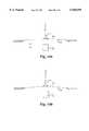
- FIGS. 1a to 1jshow a dielectric and semiconductor membrane substrate in cross-section.
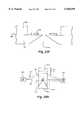
- FIG. 2shows an etched silicon substrate membrane in cross-section.
- FIGS. 3a, 3bshow dielectric membranes with semiconductor devices.
- FIG. 4shows an alignment mark of a circuit membrane in cross-section.
- FIG. 5shows support structures for a membrane structure isolation structure.
- FIG. 6a to 6ishow a circuit membrane Air Tunnel structure.
- FIG. 7shows stacked circuit membranes with optical input/output.
- FIG. 8shows a three dimensional circuit membrane.
- FIGS. 9a to 9jshow fabrication of a MOSFET in a membrane.
- FIGS. 10a to 10dshow fabrication of a transistor by lateral epitaxial growth on a membrane.
- FIGS. 11a to 11fshow vertical MOSFET and bipolar transistors formed on a membrane.
- FIG. 12a to 12gshow transistor fabrication on a membrane using confined laterally doped epitaxy.
- FIGS. 12h to 12jshow cross-sections of selective epitaxial growth on a membrane.
- FIGS. 13a to 13dshow cross-sections of multi-chip modules.
- FIG. 14shows a cross-section of a membrane formed on a reusable substrate.
- FIG. 15shows a cross-section of the membrane of FIG. 14 with a support frame attached.
- FIGS. 16a, 16bshow multi-chip modules in packages.
- FIGS. 17a to 17cshow soldering of bond pads of a circuit membrane to a die.
- FIG. 18shows bond pads on a die.
- FIGS. 19a, 19bshow bonding and de-bonding of a die to a circuit membrane.
- FIGS. 20, 21show two sides of a circuit membrane.
- FIGS. 22a to 22cshow formation of a metal trace in a circuit membrane by a lift-off process.
- FIGS. 23a, 23bshow use of a buried etch stop layer to form a circuit membrane having a thinner inner portion.
- FIGS. 24, 25show a source-integrated light valve for direct write lithography.
- FIGS. 26, 27are cross-sections of X-ray sources for the device of FIGS. 24, 25.
- FIGS. 28a to 28bshow a coil for the device of FIG. 24.
- FIGS. 29a to 29kshow portions of a source-external radiation valve for direct write lithography device.
- FIGS. 29l to 29pshow use of fixed freestanding membrane lithography masks.
- FIG. 30shows a cross-section of a lithographic tool.
- FIGS. 31a to 31cshow cross-sections of a display formed on a membrane.
- FIGS. 32a, 32bshow bonding of two circuit membranes.
- the MDI processis the formation of an IC or interconnect metallization circuit as a free standing dielectric and/or semiconductor circuit membrane.
- Each semiconductor device comprising an IC circuit membraneis a semiconductor device optionally isolated from adjoining semiconductor devices, and where each semiconductor device is formed on or in a membrane of semiconductor material typically less than 8 ⁇ m in thickness.
- the overall thickness of a circuit membraneis typically less than 50 ⁇ m and preferably less than 8 ⁇ m.
- the dielectric membraneis compatible with most higher temperature IC processing techniques.
- Heavily boron dopedtypically greater than 10 18 atoms/cm 2
- etch stop layerformed by diffusion, implant or epitaxy
- optional epitaxial SiGeless than 20% Ge
- O 2 (oxide) and N 2 (Nitride) implant etch stop barrier layerimplant etch stop barrier layer. Implant concentrations are typically between 10 to 100 times less for formation of an etch stop barrier layer than that required to form a buried oxide or nitride dielectric isolation layer as presently done with a standard thickness silicon substrate.
- Buried oxide etch stop barrier layerformed from a porous silicon layer.
- the MDI processrequires that the semiconductor membrane forming process (thinning process) produce a highly uniform membrane typically less than 2 ⁇ m thick and that the surface tension of the semiconductor membrane be in low tensile stress. If the membrane is not in tensile stress, but in compressive stress, surface flatness and membrane structural integrity will in many cases be inadequate for subsequent device fabrication steps or the ability to form a sufficiently durable free standing membrane.
- a heavily doped boron layerwill etch 10 to 100 times slower than the rest of the substrate.
- the SiGe layers and the barrier etch stop layersare subsequently removed after formation of the membrane in order to complete device dielectric isolation.
- the MDI process for forming a dielectric membranerequires that the dielectric material be deposited in net surface tensile stress and that the tensile surface stress level be 2 to 100 times less than the fracture strength of the dielectric. Consideration is also given to matching the coefficient of thermal expansion of the semiconductor material and the various dielectric materials being used in order to minimize the extrinsic net surface stress of the membrane.
- Thermally formed silicon dioxideforms as a strongly compressive film and most deposited dielectrics currently in use form typically with compressive surface stress.
- High temperature silicon dioxide and silicon nitride dielectric deposited films with tensile surface stress levels 100 times less than their fracture strengthhave been demonstrated as large area free standing membranes consistent with the requirements of the MDI process.
- the ability to form large durable temperature tolerant low tensile stress films of both semiconductor and dielectric materials as components or layers of a substrate for the fabrication of integrated circuits and interconnect structuresis unique to the MDI process.
- the large free standing semiconductor and dielectric membrane substrates of the MDI processprovide unique structural advantages to lower the cost and complexity of circuit fabrication and enhance the performance of circuit operation.
- the MDI processcan be broadly described as two methods, depending on which method of forming the semiconductor substrate thin film is selected.
- the sequence of steps of the two process methods presented belowmay be utilized in a different order depending on processing efficiencies. Formation of polysilicon or a-Si (amorphous silicon) circuit devices on a dielectric membrane without the starting use of a semiconductor substrate is disclosed below, but is not categorized as a method.
- step 3semiconductor devices if not done in step 3.
- Method #1fabricates the desired semiconductor devices of an IC on a standard thickness semiconductor substrate 10 prior to the deposition of the low stress dielectric membrane and release of membrane structure 14 by etching the back side of the substrate.
- FIG. 1ashows in cross-sections the substrate 10 after back side etching.
- These semiconductor deviceswill typically be trench isolated (see below) through or below the active area layer of each semiconductor device.
- the semiconductor deviceswill typically be fabricated from vapor phase epitaxial depositions.
- Well known epitaxial fabrication methodssuch as SEG (Selective Epitaxial Growth), ELO (Epitaxial Lateral Overgrowth), MOCVD (Metal-Organic Chemical Vapor Deposition) or MBE (Molecular Beam Epitaxy) may be employed.
- an etch stop barrier layer 12is implanted just beneath the surface of the silicon substrate 10. This is shown in FIG. 1b, which is an expanded view of a portion of substrate 10 prior to the backside etching step. Portion 11 of substrate 10 is to be removed.
- This barrier etch stop layer 12may be an oxide layer produced in a manner similar to the well known SIMOX technique or an implanted silicon nitride layer; however, the thickness of the buried oxide or nitride layer required for MDI processing is significantly less than that required to achieve device dielectric isolation for a silicon substrate which is the general application for such implant technology.
- the term SIMOX(Separation by IMplanted OXygen) is a general reference for the dielectric isolation process of forming a buried layer of SiO 2 in a bulk silicon substrate by oxygen implant.)
- the purpose of layer 12is to induce minimum damage to the crystalline surface of the substrate 10 which would degrade subsequent semiconductor device processing, while providing a uniform substrate (silicon) preferential back side etch stop just beneath the surface of the substrate.
- the barrier etch stop layer 12can be made at a well controlled thickness and acts as an end point when the silicon substrate 10 is selectively etched from the back side 14 (see FIG. 1a) as part of the processing in forming the low stress dielectric and (optionally) semiconductor circuit membrane.
- the barrier etch stop 12 as shown in FIG. 1bdoes not extend to the edge of the substrate. It is not restricted from extending to the edge of the substrate (wafer), but it must extend beyond that portion 11 of the substrate 10 that will be removed during the formation of the membrane structure.
- the original substrate upon which the MDI circuit membrane is formedserves as retaining frame (or ring) 18 for the MDI circuit membrane after the backside of the substrate is etched.
- the backside etch of the substrateleaves the frame 18 of the substrate to hold the resulting circuit membrane.
- the width of frame 18is sufficient to prevent the surface forces of the circuit membrane from causing the frame to crack.
- a width typically of less than 400 mils (1 cm)is sufficient. This is done by growing thermal oxide and or depositing a film typically of silicon nitride (about 5,000 ⁇ to 7,500 ⁇ thick) on the backside 14 of the substrate and then etching a window or opening in dielectric layer the size and shape of the desired circuit membrane.
- the substrateis then etched through dielectric window or dielectric mask.
- the shape of the backside window opening (or dielectric mask)is typically rectangular, although it can vary in shape.
- the barrier etch stop layer 12is then selectively etched to leave only the original surface 10 layer of the silicon substrate.
- a barrier etch stop layercould also be formed on the surface of the silicon substrate if the layer preserves sufficient crystalline structure required for subsequent epitaxial processing, surface stress (typically less than 10 8 dynes/cm 2 tensile) and there is a selective etch procedure for the silicon substrate versus the barrier etch stop layer, and if need be, the applied barrier etch stop layer can subsequently be removed.
- the backside 14is etched away by TMAH (tetra-methyl ammonia hydroxide) or other appropriate selective silicon etchant (see below).
- TMAHtetra-methyl ammonia hydroxide
- FIG. 1cshows formation of the semiconductor devices 24, 26, 28 in the semiconductor substrate after backside substrate etch to a buried etch stop layer, dielectric deposition, and selective removal of the barrier etch stop. Trenches 25, 27, 29 are cut into the substrate 10 prior to deposition of the low stress dielectric membrane 20, which also serves as an isolation dielectric between adjacent semiconductor devices 24, 26, 28.
- FIG. 1dshows in cross-section several transistors 11a, 11b, 11c of a circuit membrane 20 with semiconductor layer 20b, interconnect metallization 20c, low stress dielectric membrane 20d, and with completed topside device processing and a backside deposited low stress silicon nitride mask 13 patterned with openings 15a, 15b between transistors.
- LOCOSLOCal Oxidation of Silicon
- the thermal oxide isolation created by the LOCOS methodmay change the net tensile surface stress of the semiconductor (substrate) membrane layer.
- the deposition of low stress dielectric films on either side of the semiconductor layer prior to LOCOS processingwill offset most compressive effects of the oxide formation.
- Device isolation by the LOCOS process when applied to a MDI circuit membraneis more effective than current bulk processing because of the shallow depth of the semiconductor substrate layer. This also allows near optimum density of the circuit devices with respect to minimum device isolation separation.
- the easy incorporation of LOCOS into the MDI processing methodsalso is an indication of the general compatibility of the MDI process with existing IC fabrication techniques.
- the remaining substrate 10is then (optionally) bonded at its edges to a bonding frame or ring 19 (which is typically of glass, quartz or metal and about 25 to 100 mills thick) by conventional anodic, fusion (thermal) or epoxy bonding techniques.
- a bonding frame or ring 19which is typically of glass, quartz or metal and about 25 to 100 mills thick
- the substrate frame 18may be removed (see FIG. 1g).
- the bonding frame or ring 19is not required for processing MDI; the original substrate 10 (which is backside etched) performs this function initially.
- An alternative to forming a barrier etch stop layeris to polish the silicon wafer 10 on both sides to a thickness uniformity specification such that when the substrate is selectively time etched from the back side, the etch can be stopped prior to reaching the dielectric membrane 20 and will leave an acceptably uniform thickness for the active device substrate.
- This methodis mechanically difficult in that it requires the wafer to be exactingly polished on both sides to achieve the uniform thickness.
- the dielectric membrane 20, 36is formed as part of the interconnect metallization dielectric and as a layer over the two-sided interconnect metallization 35 as shown in FIGS. 3a and 3b. (FIG. 3b is an enlarged view of the portion of FIG. 3a referenced as "3b".)
- the thickness of the dielectric membrane 20, 36may vary from less than 2 ⁇ m to over 15 ⁇ m per layer of interconnect metallization layer 35. All blanket dielectric material covering the substrate has a low stress surface tension and is preferably in tensile stress.
- Two sided interconnect metallization 35, with low stress dielectric material 36 (see FIG. 3b) used as the interconnect dielectriccan be applied, or the back side of the circuit membrane can be passivated with low stress dielectric for a conventional one-side interconnect structure.
- the circuit membranecan withstand processing temperatures in excess of 400° C. which is required for further deposition of various low stress dielectric layers such as SiO 2 and Si x N x and to achieve reliable low resistance junctions between semiconductor device electrode contacts and interconnect metallization.
- higher temperature processing stepscan be performed such as may be required by implant activation annealing or epitaxial processing.
- the alignment of lithography tools on the back side of the substrateis performed through the transparent dielectric material as shown in FIG. 4.
- the semiconductor substrate material 10a near the alignment mark 40(which is nearly transparent in the visible portion of the spectrum at thicknesses less than 2 ⁇ m) can be etched away from the dielectric membrane 20 so that the lithography alignment marks 40 are more readily visible.
- Infrared alignment mechanismsare also available for back side alignment; silicon is transparent at infrared wavelengths.
- Lithography marks 40 for infrared alignmentcannot be as small as those used in the visible spectrum due to the longer wavelengths of the infrared, typically greater than 6,000 ⁇ .
- IC processing steps used on the top side and backside of the semiconductor membrane substrateare well known and not unique in application to the semiconductor substrate membrane; nearly any semiconductor process technique can be applied.
- Method #2fabricates a thin low stress semiconductor substrate membrane 20, such as the one shown in FIG. 2, prior to deposition of the low stress dielectric membrane and fabrication of semiconductor devices.
- This substrate membrane as shown in FIG. 2can be formed through established selective electro-chemical etching techniques or by combination of wafer bonding, grinding and selective substrate etching techniques.
- the membranepreferably has a tensile stress of approximately 10 8 dynes/cm 2 . (This can be achieved in one manner by forming a layer with n-type dopant concentrations of 10 16 to 10 19 atoms/cm 2 and applying electrochemical etch techniques.)
- semiconductor substrate membrane 20is fabricated (see FIG. 3a), semiconductor devices 24, 26, 28, . . .
- the low stress dielectric membrane formed on the semiconductor substratebecomes the only structural circuit membrane component after the semiconductor substrate portion of the membrane is etched or trenched into independent semiconductor devices.
- An additional layer (not shown) of low stress dielectric over the interconnect metallizationmay be applied for passivation and to increase the thickness of the resulting membrane 20 to achieve a specific desired level of durability.
- the back side etch of the semiconductor substrate 14permits the under side of the semiconductor devices 24, . . . , 30 to be accessed and additional processing of the semiconductor devices performed.
- the processing options on the under side of the semiconductor devices 24, . . . , 30are the same as those for Method #1; however, trench isolation (see FIG. 1c) of the semiconductor devices has not as yet been performed.
- Trench isolationis the etching of a separation space 25, 27, 29 (typically less than 2 ⁇ m wide) between semiconductor devices 24, 26, 28 on all sides of the semiconductor devices and is an established IC process technique. The space or trench 25, 27, 29 is then filled with dielectric.
- Trench isolationis novel as applied here, because the technique is being applied to a semiconductor membrane supported by a dielectric membrane. If trench isolation is desired, established masking and etching techniques can be applied to form trenches.
- the uniformity of the semiconductor substrate thicknessis important to the uniformity of the operating characteristics of the semiconductor devices of an IC, and to lithography processing steps.
- the above-described embodimentsuse etch stop techniques when selectively etching the semiconductor substrate material to form the desired substrate membrane thickness.
- the interconnect circuit membranecan also be formed on a glass or quartz substrate 23 (typically less than 50 mils thick).
- a tensile film 25 of polysilicon(as taught by L. E. Trimble and G. E. Celler in "Evaluation of polycrystalline silicon membranes on fused silica” J. Vac. Sci. Technology B7(6), Nov/Dec 1989) is deposited on both sides of the substrate 23, as shown in FIG. 1h.
- a MDI interconnect circuit membrane 27is then formed on the polysilicon membrane 25, as shown in FIG. 1i.
- An opening 29 in the polysilicon 25 on the backside of the substrate 23is made and the back of the substrate 23 is selectively etched leaving a free standing tensile polysilicon membrane 27 held in the frame 23b of the remaining substrate, as shown in FIG. 1j.
- the polysilicon 25 directly beneath the circuit membrane 27can optionally be removed as also shown in FIG. 1j.
- a metal film (not shown) or other protective layeris deposited over the circuit membrane prior to etching the backside of the substrate to protect the circuit membrane from the substrate etchant.
- Low stress dielectric membraneshave been manufactured consistent with MDI requirements for low stress high temperature dielectric films. These membranes were produced on Novellus Systems, Inc. (San Jose, Calif.) Concept One dielectric deposition equipment, but are not limited to such equipment. Low stress is defined relative to the silicon dioxide and silicon nitride deposition made with the Novellus equipment as being less than 8 ⁇ 10 8 dynes/cm 2 (preferably 1 ⁇ 10 7 dynes/cm 2 ) in tension. Acceptable surface stress levels of different dielectrics made on various equipment may vary widely.
- FIG. 5shows a structurally enhanced MDI circuit membrane structure. Structural enhancement of the MDI circuit membrane may prove necessary for various applications where stress is applied to the membrane as part of normal operation, such as in pressure sensing or in making contact test measurements as in IC wafer sort testing.
- a portion 44 of the dielectric membraneis deposited over the SD layer 24a with a thickness greater than 1 ⁇ m, and typically 10 to 25 ⁇ m. This thicker deposited layer 44 of the dielectric membrane is patterned with a mask and dry etched to achieve a honeycomb-like pattern of recesses 46a, 46b, 46c. The depth of these recesses 46a, 46b, 46c is approximately 75% of the thickness of the low stress dielectric 44 in which they are etched.
- Optional electrical contact 47is provided and shown as an example of a circuit electrode.
- the dimensions of the opening of the recesses 46a, 46b, 46care typically two or three times the depth dimension.
- a deposition of 1,000 ⁇ of low stress CVD silicon nitridemay optionally be applied to form a passivating seal.
- the impedance of metal conductors (traces) that make up the interconnect metallization between semiconductor devices and passive circuit elements such as capacitors or resistorsmust be given careful design consideration at operational frequencies in excess of 100 MHz.
- the dielectric constant of a dielectric (insulating) materialis a primary determining factor when consideration is given to the use of the material.
- Polyimide materials conventionally used in the construction of interconnect structureshave dielectric constants typically ranging between 2 and 3.5.
- the dielectric constants of CVD silicon dioxide and silicon nitridetypically range upward from 3.5.
- the ideal dielectricis vacuum, gaseous or air with a dielectric constant of approximately unity.
- Air Bridgesare fabricated on the surface of an IC contacting the surface of the IC only periodically. This periodic contact provides mechanical support and or electrical contact with a low net dielectric constant of isolation. Air Bridges are conventionally used in the fabrication of microwave circuits; such circuits have operational frequencies in the GHz range.
- FIGS. 6a, 6b and 6cshow cross-sectional views of a conductor structure 50 internal to dielectric layer 52, 52a, but which has a gaseous primary surface dielectric contact with only periodic mechanical contact 50-a, 50-b, 50-c, like the conventional Air Bridge.
- the conductor 50is held suspended in the gaseous dielectric without contacting the surrounding or enclosing solid material structures.
- FIG. 6dis a top view of a portion of a conductor or trace showing column supports (and/or via contacts) 50-a, 50-b, 50-c and dielectric support columns 52-a, 52-b.
- This interconnect structureis herein called an "Air Tunnel", and its method of fabrication is a direct extension of the methods used in the above-described fabrication of the MDI circuit membranes (dielectric and semiconductor membranes).
- dielectric membrane 56Also shown in FIGS. 6a, 6b and 6c are dielectric membrane 56, semiconductor membrane 58, dielectric support column 52a, ground plane metallization 60, cavity 54 formed by etch removal of a-Si (amorphous silicon), and opening 62 for etch removal of all the a-Si.
- FIG. 6bis an end-on view of an alternate structure to FIG. 6a.
- FIG. 6bshows dielectric plug contact 68 to support (suspend) conductor 50.
- FIG. 6cshows an extension of the structure of FIG. 6a with a second layer of dielectric 70 and traces 72.
- the Air Tunnel structurecan be fabricated on any semiconductor substrate in addition to an MDI circuit membrane.
- the structural dielectric materials usedare selected from the same group of low stress dielectrics used in the fabrication of the MDI circuit membranes discussed above.
- the fabrication method for the Air Tunnel provided herecan also be extended to the gaseous dielectric isolation of semiconductor devices and passive circuit elements in a circuit membrane.
- the Air Tunnel structure in one embodimentis fabricated with CVD processing techniques; alternatively, ECR (Electron-Cyclotron-Resonance) plasma CVD processing may soon provide an alternative deposition method.
- ECRElectro-Cyclotron-Resonance
- the gaseous dielectric separation of a conductor or a semiconductor deviceis accomplished by forming a sacrificial CVD film of a-Si, polysilicon or alternate material (typically dielectric material) that can be deposited by CVD means and selectively etched versus the other MDI circuit membrane material layers.
- Air Tunnel interconnect structuresin the fabrication of a circuit membrane, semiconductor devices are isolated (passivated) by trench isolation of each device, and depositing a thin layer of oxide or nitride (typically less than 2,000 ⁇ thick) over exposed device surfaces, and then depositing a film of a-Si.
- the thickness of the a-Si film and the width of the isolation trenchare chosen such that the trench is plugged or filled evenly leaving the surface over the plug relatively planar. This plug technique is facilitated by CVD process technology which deposits films conformally on all interacting surfaces.
- Subsequent Air Tunnel interconnect structuresare completed and the a-Si layers are removed by a silicon selective etchant; the etchant accesses the a-Si through the etch-vias as explained below.
- the fabrication method of Air Tunnel interconnectionis independent of the underlying substrate.
- the underlying substratecould be a MDI circuit membrane as shown in FIG. 6d (fabrication of which is disclosed above), a conventional IC substrate of semiconductor devices, a MCM circuit substrate, MDI tester surface membrane, etc.
- the Air Tunnel fabrication processbegins (see FIG. 6f) with the deposition of an a-Si film 76 onto a substrate 56 with electrodes to be interconnected.
- the a-Si film 76is patterned with trenches and contact vias.
- a CVD processed metal film 50typically tungsten (W) is deposited over the a-Si.
- the dimensions of the a-Si trenches and vias in the a-Si layerare consistent with forming planar plugs.
- the trenches in the a-Si 76once plugged with the metal film 50, become the support columns 50-a, 50-b, 50-c of the conductor, see FIGS. 6a and 6d.
- the conductors deposited in the viasprovide mechanical (column) support and electrical contact.
- the metal film 50is patterned and a second CVD processed a-Si film 78 deposited over the metal film 50; a thin layer (not shown in FIG. 6a) of highly conductive metal like Au or Cu may be sputter deposited over the CVD metal (prior to the patterning of the metal film 50) to enhance conductivity of the conductor.
- the a-Si film 78is patterned as shown in FIG. 6f, removing the a-Si film 78 from over the metal conductor 50 and forming a trench 80 along the edge of the conductor 50. This trench is plugged by a 3rd CVD layer 82 of a-Si, as shown in FIG. 6g.
- the patterning of the second a-Si layer 78 over the metal conductor 50does not require a critical alignment; an alignment tolerance of +50% of the thickness of the second a-Si layer 78 is sufficient.
- the resulting three films 76, 78, 82 of a-Siare relatively planar with minor surface features along the edges where conductors 50 are directly beneath. These surface features can be reduced by shallow thermal oxidation of the a-Si surface and subsequent stripping of the oxide (not shown).
- An alternative method that can be used to planarize the a-Si and metal filmsis to spin coat a thick polymer over substrate 75, low stress dielectric 77, first a-Si layer 79, and second a-Si layer 81 after the application of the second a-Si film 81.
- This a-Si film 81is deposited in thickness equal to the combination of the former second and third a-Si films.
- the polymer 85 usedis selected to have a RIE rate nearly identical to the that of the a-Si film. The polymer 85 is completely removed and the etch of the a-Si is continued as desired, see FIGS. 6h and 6i.
- the a-Si film stackis then patterned to form trenches that will become the supporting columns 50-a, 50-b, 50-c of an over layer of low stress dielectric.
- These support columnsare typically placed in a non-continuous manner along conductors 50 (as shown in FIG. 6d), and periodically placed across open areas 51 where there are not conductors.
- the periodic and overlapping placement of the support columns (etch-vias)increase the ability of a-Si selective etchant to remove all deposited a-Si material.
- the thin metal film 60see FIG.
- a low stress dielectric film 52, 52ais deposited of typically 1-2 ⁇ m thickness over the patterned a-Si films. This low stress dielectric layer 52, 52a is patterned with trench openings 62 to the a-Si films.
- trench openingsare called etch-vias and provide access for a a-Si selective etchant like TMAH or ethylene diamine to remove all of the internal layers of a-Si films from each layer of interconnect without regard to the number of layers.
- a a-Si selective etchantlike TMAH or ethylene diamine
- the etch-vias 62 in the dielectricare placed near dielectric support columns as shown in FIGS. 6c and 6d.
- the etch-vias 62are placed on every interconnect layer and with sufficient frequency per layer to allow etchant to reach all lower layers of the Air Tunnel interconnect structure.
- an additional interconnect layer 72, 80can be formed by repeating the sequence of process steps as outlined below.
- the etch-vias 62serve as access ports for gaseous material (such as N 2 or air) which allow the effective circuit dielectrics to enter the circuit membrane.
- gaseous materialsuch as N 2 or air
- the etch-vias 62also serve to maintain equalized pressure between the internal interconnect structure and the external environment of the surface of the circuit.
- Steps 6 through 8 from abovecan be replaced with the following alternative steps for forming a planarized conductor layer:
- the principle attributes of the Air Tunnelare:
- FIG. 6eA MOSFET device connected by Air Tunnels is shown in cross-section as an example in FIG. 6e.
- the transistor of FIG. 6eis formed from a semiconductor membrane and held suspended by the metal contacts to its electrodes with a gaseous dielectric separation on all remaining device surfaces. Shown in FIG. 6e are the active portion 84 (MOSFET) and the unused portion 86 of the semiconductor membrane, a thin nitride isolation film 88, mechanical conductor support 94, conductor trace 92, and additional air tunnel interconnect structures 92, 94, 96.
- MOSFETactive portion 84
- FIG. 6eShownitride isolation film 88, mechanical conductor support 94, conductor trace 92, and additional air tunnel interconnect structures 92, 94, 96.
- circuit membranesThe fabrication of circuit membranes provides the capability to fabricate and use integrated circuits in novel ways such as:
- optical communicationin a vertically arrayed stack of MDI circuit membranes 150a, 150b, 150c with optical transmit and receive semiconductor devices on either side of the circuit membranes. Busing of data through a stack of several MDI circuit membranes 150a, 150b, 150c from any point on the surface of an IC rather than forming connections at the edge of ICs (which is currently the practice) simplifies the structure of the circuit.
- An external communication optical transceiver 152is provided.
- MDI circuit membrane 150bincludes a transparent window 154 through which optical transmissions from transmitters (laser diode arrays) 156 pass to optical receiver SDs 158.
- the stack of MDI circuit membranesis held together by support 160.
- the ability to use optical means rather than metal conductors to transmit information between ICsshortens the length of the communication path, increases the speed and bandwidth of the communication path, and lowers the power consumed compared to present metal connection methods.
- the optical receiver of the MDI circuit membraneis typically less than 5,000 ⁇ in thickness. A receiver of this thickness will absorb only a portion of the optical signal fluence striking it, the remainder of the fluence will pass through and out the opposite side of the receiver. This permits a second or third receiver to be positioned in the path of the optical transmitter to receive the same signal.
- the limiting conditions that determine the number of receivers that can be associated with one transmitterare the output fluence of the optical transmitter and the thickness of the transceiver substrate. This ability to optically transmit to several receivers simultaneously has the benefits of reducing circuit complexity (versus a transceiver structure at every circuit membrane interface) and performance (no transceiver (repeater) propagation delay).
- circuit membranes 160a, 160b, 160c including SDs 162, 164, 166are by compression bonding of circuit membrane surface electrodes 168a, 168b, 168c, 168d (pads).
- Bonding 170 between MDI circuit membranesis achieved by aligning bond pads 168c, 168d (typically between 4 ⁇ m and 25 ⁇ m in diameter) on the surface of two MDI circuit membranes 160b, 160c and using a mechanical or gas pressure source to press the bond pads 168c, 168d together.
- the pads 168c, 168dare solder, they can be heated to the melting point of the solder (typically less than 350° C.) causing the pads to weld to each other. If the pads are indium, tins or alloys of such metals, a bond 170 will form between the metal pads 168c, 168d with the application of approximately 100 p.s.i. pressure and an application temperature between 50° C. and 400° C., depending on the metal or alloy selected.
- FIGS. 9a to 9eshow a sequence of steps for forming a p-channel or n-channel (npn) transistor with an opposed gate electrode and a gate width of less than 25 nm (250 ⁇ ).
- the process steps(see FIG. 9a) assume a starting substrate of an MDI circuit membrane with approximately 0.5 to 1.5 ⁇ m wide isolated metal gate electrode 174 fabricated on the backside (opposed) of the transistor.
- This MDI circuit membraneconsists of a lightly doped ⁇ 100> crystalline silicon membrane layer 176 of thickness typically less than 2 ⁇ m and a 1 to 2 ⁇ m layer of low stress dielectric 178.
- FIG. 9bshows one such well 180. This is done by depositing a nitride layer 182 over the silicon layer 176 of the MDI circuit membrane, patterning the well 180 and implanting the desired dopant.
- a metal layer 190such as tungsten of 0.5 to 1.5 ⁇ m, but of known thickness, just closing the V-groove 186.
- the reliable fabrication of the gate region 194 at a known lengthis dependent on etch rate control.
- Present etch rate techniquessupport the capability to form a gate region 194 length of less than 25 nm.
- a CVD dielectriccould also be used as the gate implant mask instead of a metal plug 90.
- This gate fabrication methodcan also be done in bulk silicon and is not limited to the MDI process. It is important to note that the sub-micron resolution of the gate region was achieved without lithographic means capable of sub-micron resolution.
- FIGS. 9f, g, h, i & jshow the process sequence for substrate-imaged nonlithographic MOS transistor gate region or Bipolar emitter region formation.
- This processtakes advantage of the novel ability of the MDI structure to accommodate process steps on either side of the membrane substrate.
- This processcan form a minimum feature size of less than 100 nm and does so by the use of anisotropic etching epitaxial processes.
- FIG. 9fshows a MDI substrate of semiconductor 189 and low stress dielectric 191 formed by one of the methods presented above.
- the dielectric layer 191 on one sidehas been patterned and the semiconductor layer 189 anisotropically etched through to the dielectric layer 193 on the opposite side.
- the thickness of the semiconductor layer 189is selected to be less than 2 ⁇ m, and the dielectric layers 191, 193 are less than 1 ⁇ m thick each, though these dimensions can be scaled to achieve any transistor dimensions.
- the size of the patterned opening 195 in the dielectricis chosen such that the etched opening 197 onto the underlying surface of the dielectric is a desired width, less than 100 nm.
- the patterned dielectric 191has a 1,000-2,000 ⁇ layer 199 of low stress silicon nitride to provide high selectivity versus the opposed dielectric layer-during a subsequent RIE process step.
- FIG. 9gshows an opening 197 formed through the dielectric layer 193 opposite the patterned layer 191.
- the anisotropically etched semiconductor layer 189 with its opening 197 onto the under side of the opposite side dielectricwas used as a substrate-imaging mask, and the dielectric layer 193 was etched by RIE (dry) processing.
- This substrate-imaged opening 197can be less than 100 nm in diameter and will become the gate region of a MOS transistor or the emitter region of a bipolar transistor.
- FIG. 9hshows the substrate-imaged region 197 closed by selective epitaxial growth 201; the epitaxial growth 201 can be formed with a graded dopant structure to lessen short channel effects.
- FIG. 9hshows the substrate-imaged region 197 closed by selective epitaxial growth 201; the epitaxial growth 201 can be formed with a graded dopant structure to lessen short channel effects.
- 9ishows the formation of a gate oxide 203 and electrode 205 after a planarization step of the self-imaged opening 197, CVD or thermal formed gate oxide and formation of gate electrode. It is important to note that the dielectric layer 193 in which the gate electrode 205 is formed is self-aligned to the gate region.
- FIG. 9jshows the finished MOS transistor.
- the side opposite the gate electrode 205is stripped of dielectric, planarized and etched to a thickness of less than 2,500 ⁇ . It was then trenched 207 for source/drain isolation, a layer of low stress dielectric 209 deposited and source/drain electrodes 211, 213 formed.
- bipolar transistorcan be formed with somewhat similar fabrication steps.
- FIGS. 10a, b, c, & dshow a method for forming a MOSFET transistor with transistor gate region lengths of sub-micron dimensions, without the requirement for lithography tools with sub-micron CD resolution capability. This method is an extension of the above-described MDI process technology.
- the starting substrate structureis a combination silicon and dielectric 204 film forming a membrane 202.
- This membrane 202is formed by one of the methods disclosed above. Subsequently, membrane 202 is patterned for the doping of the n+ and p+ transistor channels.
- FIG. 10ashows a cross-section of a MOS transistor channel (source 210, gate 208 and drain 206 regions) with a nitride mask 212 through which an anisotropically formed gate 208 trench is etched to the underlying dielectric membrane 204 in the location where the gate region of the transistor will be constructed.
- the exposed silicon sidewall 214may be polished by a thin thermal oxidation and etch stripping or chemical techniques.
- FIG. 10bshows a top view of the structure of FIG. 10a, with the transistor channel 210, 208, 206 isolated from surrounding transistor devices by dielectrically filled trenches 216. These trenches 216 are fabricated prior to etching the gate region trench 208.
- the gate region trench 208is then filled (see FIG. 10c) from both silicon sidewalls by lateral selective epitaxial growth of silicon 220 and with the same or similar doping concentration as the adjacent regions 210, 206; source and drain implant doping can also be used as a doping means prior to epitaxially growing the gate region.
- source and drain implant dopingcan also be used as a doping means prior to epitaxially growing the gate region.
- the epitaxial growth process in the gate region trench 208is stopped when the remaining separation distance "d" between the approaching silicon sidewalls 220 is equal to the desired gate region length.
- the doping concentrationis changed for forming the actual gate region 222, and the epitaxial growth is continued until the gate region trench is closed, as shown in FIGS. 10c and 10d.
- the width of the initial gate region trench 208 and the epitaxial growth ratecan be controlled with an error of less than 5 nm. This allows the length d of the gate region to be determined by the precision with which the gate region trench 208 can be formed, the deposition rate control of the lateral epitaxial growth 220 and the capability to create the desired doping transitions. The result of this approach means that a gate region length d of 25 nm or less can be formed. This is far beyond the current optical lithographic methods which are presently expected to reach production capability of 120 nm by the end of the decade.
- FIG. 10dshows the completion of the transistor with source and drain electrodes 226, 224, and an opposed gate electrode 230.
- the surface of the epitaxially grown gate region 222is not smooth, but the backside of the gate region 222 is smooth, due to its formation against the underlying low stress dielectric membrane 204.
- the gate electrode 230is more easily and reliably formed by patterning the underlying dielectric membrane 204 from its backside, thereby forming the opposed gate electrode 230.
- the backside of the gate region 222is etched free of dielectric with an opening significantly larger than the length d of the epitaxially grown gate region 222; portions of the source 210 and drain 206 regions are also exposed with the gate region due to lithographic tool limitations.
- Gate oxide isolation 232is thermally grown or deposited to the required thickness, and a metal or silicide electrode is formed 230.
- the overlap of the gate electrode 230 over the source 210 and drain 206 regions of the transistor channelresults undesirably in performance limiting capacitance.
- the reduction of the capacitance from the overlapping gate electrode structurecan be achieved by either epitaxial graded doping of the source and drain regions at the interface to the gate region growth over the gate region, to form an extended gate region, or by offset of the gate electrode so that the source side edge of the electrode aligns approximately with the source/gate interface of the transistor channel.
- the MDI circuit membrane structureprovides the capability to position electrode contacts of semiconductor devices at their backside (or opposed side). This provides significant savings in reduced processing steps to achieve device isolation and new transistor structures.
- FIG. 11ashows a MDI circuit membrane (dielectric 240 and semiconductor 242 films) in cross-section on which additional semiconductor layers were formed epitaxially to achieve either an npn or pnp transistor structure 244.
- the epitaxial layer 244-a that corresponds to the gate regioncan be formed with a thickness of less than 25 nm.
- FIG. 11bshows the dielectric 240 and semiconductor 247, 244, 245 membrane after subsequent well known semiconductor processing steps which form a transistor channel 244 isolated on the dielectric membrane 240 with source 246, drain 248 and gate electrodes 250-a, 250-b attached. Also shown are source region 245 and drain region 247.
- the gate oxide isolation 251is thermally grown or deposited, and gate contacts 250-a, 250-b can be formed on one or all sides of the transistor channel. Alternatively, a separate contact 250-b can be formed opposite the gate electrode 250-a, and used as a transistor bias contact.
- the opposed drain contact 248is formed by etching a via in the dielectric membrane 240 underlying the transistor drain region 247.
- FIG. 11cshows a bipolar transistor formed by a well known method but on a low stress dielectric membrane 254, and without the requirement to form a lateral conductive path (typically referred to as a buried layer).
- semiconductor film 256Formed in semiconductor film 256 are emitter 258, base 260, and collector 262 regions. The collector contact 264 is instead formed directly under the emitter 258.
- non-silicon semiconductor transistor structuresthat can be restructured with a backside contact as depicted in FIG. 11c, such as a GaAs Heterojunction Bipolar Transistor (HBT) or Ballistic Transistor.
- HBTGaAs Heterojunction Bipolar Transistor
- Ballistic TransistorBallistic Transistor
- GSDGraded Gate Doping
- EEGEpitaxially Extended Gate
- GEOGate Electrode Offset
- the Graded Gate Dopingis shown in FIG. 11b. This method varies the doping levels of the source 245 and drain regions 247 at their respective interfaces to the gate region. This directly decreases the effective dielectric constant of the semiconductor under the dielectric isolation 251 separating the gate electrode from the source 245 and drain 247 regions it overlaps.
- the Epitaxially Extended Gate 244-b(see FIG. 11d) is formed by selective epitaxial growth of the gate region 244-b over the surface of the transistor upon which the gate oxide 251 and gate electrode 250-a will be fabricated.
- This methodmore directly than the GGD method of FIG. 11b, lowers the capacitance of the semiconductor region directly under the gate electrode 250-a where it overlaps the source 245 and drain 247 regions.
- the transistor capacitive charging effect contributed by the gate electrode 250-a from source 245 and drain region 247 overlapis decreased by these methods, because of the dopant type and dopant concentration relative to the polarity of the applied potential on the gate electrode 250-a.
- the thickness of the epitaxial layer of the EEG methodis determined based upon the desired operating characteristics of the transistor, but typically is less than the dimension of the gate region length.
- the extended gate region 244-b of FIG. 11d formed by the Epitaxial Extended Gate methodcan also be a graded doping region. If the extended gate region 244-b is graded, the dopant concentration decreases going away form the gate region (or towards the gate electrode 250-a).
- the Gate Electrode Offset (GEO) structureis shown in FIG. 11f. Shown are source region 269, gate region 271, drain region 273, semiconductor layer 275, low stress dielectric layer 277, gate oxide 279, and offset gate electrode 281.
- the drain side edge of the gate electrode 281is aligned to the drain/gate 273-271 interface of the transistor channel. The alignment could alternately be made to the source/gate 269-271 interface, and would be a preferred structure under certain device design requirements.
- the accuracy of the placement of the electrode 281 edgeis limited by the capability of the lithography tool used.
- a gap between the drain region 273 and gate electrode 281may result leaving a portion of the gate region 271 not covered by the gate electrode 281 due to lithography alignment deficiencies. This can be corrected by extending the drain region 273 through implant doping of the exposed gate region. The size of this gap during manufacturing can reliably be expected to be no greater than the magnitude of the alignment registration error of the lithography tool being used.
- the transistor structure of FIG. 11e used as a bipolar transistoris of interest in order to achieve well controlled fabrication of thin base regions.
- the contact 270 to the base region 272 of a bipolar transistor in FIG. 11eis achieved by epitaxially extending 272-a the base region. This method like the EEG method is the selective epitaxial growth of an exposed region of the transistor that includes the base region 272.
- Other elements of FIG. 11eare collector region 274, collector contact 275, dielectric membrane 276, emitter region 277, and emitter contact 278.
- FIGS. 12a, b and cshow the use of a MDI circuit membrane to produce a confinement cavity for the epitaxial growth of crystalline silicon.
- the original objective of CLSEG, to fabricate a dielectric isolated semiconductor substrate,is not an objective here because the MDI process is itself a dielectric isolation process.
- What is taught hereis the application of the capability for growing epitaxial films in a confinement cavity within the context of the MDI process, and a processing method for using confined lateral epitaxial growth to fabricate MOSFET transistors with arbitrarily narrow gate region lengths without the use of lithographic means.
- MDI confined lateral doped epitaxialclosely controls transistor geometry in all three dimensions: height (as deposited semiconductor film thickness), width (placement of isolation trenches) and source, gate, drain regions (epitaxial deposition thickness). This makes the device operational characteristics more predictable with lower manufacturing complexity.
- the MDI Confined Lateral Epitaxy methodbegins with a membrane of two films, one film 280 of semiconductor (silicon) and one film 282 of low stress dielectric. This membrane 280, 282 is made by one of the methods disclosed above.
- Dielectric filled isolation trenches 284are fabricated to form what will become the sides of the transistor channel in the semiconductor film.
- a low stress dielectric layer 290 typically of 1 ⁇ m or less thicknessis deposited, and a window 286 is anisotropically etched through the semiconductor film 280 stopping on the dielectric layer 282 and positioned between the isolation trenches 284, as shown in FIGS. 12a and 12b.
- the orientation of the window 286is approximately aligned with the crystallographic orientation of the semiconductor film 280 in order to produce a seed crystal walls 292-a, 292-b of FIG. 12c that is at a right angle to the isolation trench walls 284, 290, 282 in the confinement cavity, as explained below.
- the transistor depth (thickness)is well controlled by the thickness of the semiconductor membrane 280 which in turn can be precisely determined by epitaxial and/or etching means.
- the exposed semiconductor film 280is then anisotropically etched back in two directions under the dielectric over layer 290 and along the isolation trenches 284 as shown in FIG. 12c.
- Thisforms a very smooth walled confinement cavity 292 with a smooth seed crystal 292-a, 292-b at the end of the cavity 292.
- the etchis stopped at a lateral depth consistent with the design requirement for the number of transistors to be formed in the confinement cavity.
- the depth "c" of the confinement cavity 292may vary from about 2 ⁇ m to over 15 ⁇ m.
- a smooth contamination free seed crystal wall 292-a, 292-bis required for the subsequent epitaxial growth.
- the crystal seed wall 292-a, 292-bwill form at an angle dependent upon the crystallographic orientation of the semiconductor film.
- a ⁇ 100> silicon filmwill form a seed wall angle of approximately 54.74° as measured from the horizonal, and a ⁇ 110> silicon film will form a seed wall 292-a, 292-b with an angle 90° (as shown in FIG. 12c).
- GaAs and InPhave similar crystallographic properties and can be used as the semiconductor film instead of silicon.
- the selective epitaxial growth of crystalline semiconductorproceeds from the seed crystal wall 292-a, 292-b.
- the npn or pnp regions of silicon MOSFET transistorsare epitaxially grown (see FIG. 12d) with in situ doping to whatever design thicknesses desired. This allows the length of the base or gate region of the transistor to be determined by the epitaxial growth process instead of a lithographic process as presently done. This also allows the length of the base or gate region of the transistor to be arbitrarily narrow, which cannot be done with current lithography methods.
- FIG. 12dshows the confinement cavity 292 filled with a CMOS transistor pair of npn and pnp structures 294, 296.
- Each region of the transistorcan be uniquely tailored to length and doping concentration level, in addition, because the transistor channel is formed by epitaxial means, doping of the transistor 294, 296 regions, can be extended to graded segments as discussed above. Further, non-symmetric doping of source and drain regions can easily be implemented by time based selection of dopant during epitaxial growth; this is not easily accomplished in bulk wafer processing due lithography limitations in resolving the gate region.
- FIG. 12dshows two pairs 294, 296 of CMOS transistors formed as mirror images of each other in two confinement cavities; this was a design choice because a single confinement cavity could have been formed by additional trench dielectric isolation of the initial confinement window opening.
- gate region lengths "g"of less than 25 nm can be fabricated.
- prior art MOSFET transistor gate regionsare predominately formed by optical lithographic means and are presently limited to minimum gate region lengths of approximately 0.5 ⁇ m (500 nm).
- FIG. 12eshows the CMOS transistor pairs 294,296 with electrode contacts 294-a, 294-b, 294-c, 296-a, 296-b, 296-c.
- the isolated gate electrodes 300, 302, 304, 306each span the narrower gate region length of the transistor.
- the gate electrodeis formed by standard lithographic processes, and may be many times of greater length than the gate region length of the transistor. For example, a lithographically defined gate electrode of 0.5 ⁇ m and a transistor gate region length of 25 nm are possible. Gate electrode capacitance attributed to the gate electrode overlap of the source or drain regions can be reduced as described above with the GGD, EEG, and GEO methods.
- FIG. 12eshows the CMOS transistor pairs 294,296 with electrode contacts 294-a, 294-b, 294-c, 296-a, 296-b, 296-c.
- the isolated gate electrodes 300, 302, 304, 306each span the narrower gate region length of the transistor
- 12fshows embodiments of all of these methods; the electrode 312 opposed to the gate electrode 308 is presented optionally as a substrate bias. Also shown in FIG. 12f are source region 294-1, optionally graded doped gate region 294-2, epitaxially extended gate regions 294-4, offset gate electrode 308, gate isolation 310, and optionally epitaxially extended substrate 312-a.
- the MDI Confined Lateral Epitaxy methodis not limited to MOSFET transistors or silicon as a semiconductor material.
- the MDI Confined Lateral Epitaxy methodcan be used to fabricate silicon bipolar transistors, or applied to other semiconductors such GaAs or InP which can be epitaxially formed.
- An example of a bipolar transistoris shown in FIG. 12g when emitter region 314, base region 316, epi-extended base and electrode 318, collector 315, and optionally epi-extended base and electrode 319.
- the semiconductor layer of a MDI circuit membraneprovides various methods to pack circuit devices densely, mix semiconductor types or simplify the fabrication steps.
- FIGS. 12h, i & jshow examples of such methods.
- FIG. 12hshows a silicon membrane 289 upon which an epitaxial dielectric 291 and a subsequent layer of epitaxial semiconductor 293 has been formed; the total thickness of this membrane structure is typically less than 4 ⁇ m.
- the dielectric layer 291should closely match the crystal lattice dimension and structure of the silicon 289; an example of such a dielectric with a similar crystal lattice is sapphire or undoped silicon under certain device design parameters.
- This MDI semiconductor layer structureallows semiconductor devices to be formed on either side of the semiconductor layer 289 and remain electrically isolated.
- CMOS integrated circuitswith p-type device formed on one side and n-type devices formed on the opposite side.
- Low stress dielectricwould be used to trench isolate individual semiconductor devices and complete the MDI process suggested by Method #2.
- the second epitaxially grown semiconductor layer 293can be a material other than silicon such as GaAs or InP.
- FIG. 12ishows a MDI circuit membrane composed of a silicon layer 295 and a low stress dielectric layer 297.
- the dielectric layer 297has been patterned to form open areas 299 into which semiconductor material was deposited by selective epitaxial growth.
- the selectively deposited semiconductor 299can be an semiconductor other than silicon, or silicon.
- Semiconductor devicescan be fabricated in the epitaxial islands 299 on the backside of the MDI semiconductor layer.
- FIG. 12jshows a MDI circuit membrane composed of a silicon layer 295 and a low stress dielectric layer 297.
- the dielectric layer 297has been patterned and silicon islands 299 formed through selective epitaxial growth in the same manner as described for FIG. 12i.
- the silicon layer 295was subsequently patterned removing portions of the silicon layer opposite each island 299 that was epitaxially grown in the dielectric layer, and then filling with low stress dielectric. Circuit devices formed in the semiconductor islands 299 are dielectrically isolated.
- This membrane structurehas similar applications as those suggested for FIG. 12h.
- FIGS. 12h, i & jshow that a two level device structure can be formed that permits more compact interconnection of the circuit devices by the use of vertical interconnections. These structures also simplify the fabrication of mixed device technologies such as BiCMOS by allowing the Bipolar and MOSFET devices to be fabricated on either side of the semiconductor membrane without an increase of interconnect complexity.
- the use of these MDI structurestypically doubles the total surface area are available for interconnect metallization routing.
- the obvious potential processing benefitscan be a reduction in the number interconnect metallization layers per side and or relaxation of the interconnect metallization pitch used, both of these benefits normally lead to an increase in circuit yield.
- the mechanical (physical) and thermal properties of the nitride and oxide free standing membranes made with the Novellus equipmentare similar to silicon membranes presently being used in the making of ICs with integrated sensors.
- Examples of such silicon membrane or diaphragm based sensorsare those made for sensing acceleration, pressure or temperature, but not limited to these areas.
- the availability of such oxide and nitride dielectrics for general applicationis novel with this disclosure.
- the use of such free standing dielectrics membranessignificantly reduces the complexity of producing a membrane with non-conducting properties in a silicon or semiconductor fabrication environment.
- the low stress dielectric membraneshave selective etchants that allow the dielectrics to be processed independently in the presents of silicon.
- the known passivating capability and inert chemical nature of silicon nitride, and the relatively similar coefficient of thermal expansion of silicon, silicon dioxide and silicon nitrideincreases the operating environmental range of sensors versus organic dielectrics.
- Sensor diaphragms of low stress dielectric membranes produced on rigid substratescan in most cases directly replace silicon membranes or be used in conjunction with a silicon membrane formed on a rigid (conventional) semiconductor substrate. No new fabrication methods are required to integrate the low stress MDI process dielectrics into such sensor ICs.
- a MDI circuit membrane with few or without active circuit devicesis called more specifically an interconnect circuit membrane.
- the interconnect circuit membranebecomes a multiple chip module (MCM) interconnect circuit membrane as discussed immediately below. This does not limit the application of a MDI circuit membrane with active and passive circuit devices from being used in the fabrication of a MCM.
- a MDI circuit membranecomposed primarily of interconnect metallization of one or several internal interconnect levels can be fabricated on a substrate to provide electrical interconnections between the bond (signal) pads of various individual dice (ICs) as in the well established packaging technique called multiple chip module (MCM).
- MCMmultiple chip module
- a MDI circuit membrane made for this type of applicationis called multi-chip module Interconnect Circuit Membrane (ICM).
- the multi-chip module interconnect circuit membraneis formed using the MDI process and conventional semiconductor processing techniques.
- the interconnect circuit membranemay have several thousands of die metal bond pad contacts or bonding points. The position of these metal contact or bonding points on the surface of the interconnect circuit membrane can be arbitrarily placed.
- the multi-chip module interconnect circuit membranecan be formed on any substrate material that can meet the requirements for flatness specification, withstand the processing temperatures of the applied low stress dielectric(s), and can be selectively etched with respect to the low stress dielectric(s) to form the circuit membrane.
- FIG. 13ashows an embodiment of an multi-chip module interconnect circuit membrane made as described above by the MDI methods.
- FIG. 13aincludes the interconnect circuit membrane 320 with several internal metallization trace layers (not shown), ICs (dice) 322a, 322b, 322c, interconnect circuit membrane substrate frame 324, and IC bonding contacts 326.
- FIG. 13bshows a related structure which is a cross-section of a functional tester for testing ICs with probe points 330 formed on attached ICs 336a, 336b.
- the interconnect circuit membranecan also be formed (see FIG. 14) using the MDI method on a quartz substrate 340 that has been coated with a release agent 342 such as KBr; this assumes that a single-crystal type membrane or substrate 340 is not required for the fabrication of various types of active circuit devices (SDS) in the interconnect circuit membrane 320.
- SDSactive circuit devices
- FIG. 15shows the multiple chip module interconnect circuit membrane 320 of FIG. 13a made with the release agent method of FIG.
- the circuit membrane made with the method utilizing polysilicon as disclosed above and shown in FIG. 1jcan also be used as an interconnect circuit membrane to achieve a similar result as that shown in FIGS. 13a, 13b and 15.
- the interconnect metallization traces in the circuit membraneform electrical connections from one or more of the contact pads of an IC to one or more contact pads of the other ICs.
- the diameter of these padscan vary from less than 0.5 mil (0.001" or 25 ⁇ m) to several mils.
- the limiting factors of the size of the IC contact padsis the lithography method used in fabrication and the assembly method; the cost of such methods increase as pad diameters less than 3 mils are employed.
- FIG. 16ashows the packaging for a version of the structure shown in FIG. 13a, including IC carrier lid 352, compressible material (such as silicone) 354 attached thereto, carrier substrate 355 of the MCM package, contacts 356 to the carrier signal pins 357.
- IC carrier lid 352compressible material (such as silicone) 354 attached thereto
- carrier substrate 355 of the MCM packagecontacts 356 to the carrier signal pins 357.
- gastight gasket 358enclosing pressurized volume 359.
- the interconnect circuit membrane 360(see FIG. 17a) is made from optically transparent dielectrics such as low stress silicon dioxide and or silicon nitride, this permits the conventional die (IC) 362 to be visually aligned on the interconnect circuit membrane 360 from the backside or from the side of the interconnect circuit membrane 360 opposite that of the die 362.
- a locally directed infrared or other heat source(not shown) can then be applied from the backside of the interconnect circuit membrane 360.
- MDI pad 365which is surrounded by solder wells 364, and solder weld bonds can be formed between the interconnect circuit membrane pads 365 and the die bond pads 366 on which is formed solder bump 367 which typically is about 5 to 25 ⁇ m thick.
- the die 362is attached face down against the interconnect circuit membrane 360.
- Solder weld bondsare formed by using a heat source (not shown) such as a high intensity lamp, laser or metal instrument that can heat the solder to its melting point.
- the heat sourcemelts the solder 367 (see FIG. 17b) directly under the die pad 360 by heating through the interconnect circuit membrane 360 while the die is in contact with the interconnect circuit membrane.
- the high temperature tolerance of the dielectric material, its innate elasticity and thin structureallow heat from the heating source to quickly reach and melt the solder 367 to form a bond of 3 to 10 ⁇ m thickness.
- the melted solder 367wets both the die pad 366 and the interconnect circuit membrane pad 365, and when it cools the solder 367 contracts holding the die pad 366 firmly against the interconnect circuit membrane pad 365.
- solder bondis formed with no more pressure than what would be exerted when the die 362 is brought in contact with the interconnect circuit membrane 360, pressing into the interconnect circuit membrane and deflecting it by less than 25 ⁇ m.
- the interconnect circuit membrane 360assumes a uniform planar contact against the surface of the die 362. This also removes the requirement that the solder on each pad be formed to an exacting equivalent height.
- the solder 367(see FIG. 17c) alternatively is originally electroplated onto the interconnect circuit membrane bond pad 365.
- the solder 367is electroplated to a height between 5 and 25 ⁇ m.
- the original height of the solder bump 367is greater than the depth of the solder well 364 of the interconnect circuit membrane 360 in which the pad 365 of the interconnect circuit membrane 360 is positioned.
- FIG. 17bshows the structure of FIG. 17c after soldering or bond formation. If a die is removed some excess solder 367 will remain on the pad 365 of the interconnect circuit membrane 360.
- a hermetic sealcan be formed between the surface of the die 362 and the interconnect circuit membrane 360. This is done by forming a metal bond along all edges of the die (not shown). This bond can be soldered, and is formed as described below.
- An advantage of the high temperature tolerance of the interconnect circuit membrane which allows die solder bonding to be done without the application of any significant contact pressure between the interconnect circuit membrane and die,is the ability (see FIG. 18 showing a top view of bond pads on a die) to place die bond pads 370-1, 370-2, . . . , 370-k, . . . , 370-n directly over the circuit structures of the die (not shown). This allows the placement of semiconductor devices directly under a bond pad 370-k without concern that the semiconductor devices will be damaged, which is the case when mechanical wire bonding equipment is used to wire bond a die to its carrier.
- Damage-free bondingis not presently possible with current die wire bonding techniques, because such bonds are compressively formed with a mechanical arm which presses, rubbing through the die bond pad into the substrate of the die to be placed anywhere on the surface of the die.
- the MDI methodmakes the design of the IC easier, removes the need for reserved pad area on the die (which saves 5 to 10% of the surface area of the die) does not restrict the placement location of the pad, and allows the pads to be larger since area under the pads is no longer reserved exclusively for them.
- a hermetic seal bond pad 372extends continuously along the perimeter of the surface of the die.
- a hermetic seal of the surface of the die with the surface of the circuit membranecan be accomplished by the formation of an enclosing solder bond (comprising a solder well as described above for forming pad bonds) along the edge of the die.
- the hermetic sealis typically also a ground contact for the die.
- the infrared solder bonding of die to the multiple chip module interconnect circuit membraneis a simple process which also allows the dies to be easily removed and replaced without damage to the interconnect circuit membrane.
- the IC 372is held by a vacuum tool 373 and aligned in close proximity to the MCM interconnect circuit membrane 374. Once aligned, the interconnect circuit membrane 374 is gently urged forward by a fluid pressure 376 a distance of several mils and the die 372 is urged toward the interconnect circuit membrane 374 until contact is established.
- the infrared heat source 377is applied to achieve localized heating of the solder pads (not shown) on the IC die 372 until they melt and wet to the interconnect circuit membrane 374.
- the die 372can be removed (see FIG. 19b) by using the same vacuum tool 373 to gently pull on the IC 372 while localized heating from heat source 377 of the IC is applied until the solder bonds melt and the IC 372 can be pulled from the interconnect circuit membrane 374; no fluid pressure is applied to the interconnect circuit membrane 374.
- the multi-chip module interconnect circuit membranecan be enhanced to include passive devices such as resistors, capacitors, and polysilicon or a-Si (amorphous-Silicon) TFTs (Thin Film Transistors).
- passive devicessuch as resistors, capacitors, and polysilicon or a-Si (amorphous-Silicon) TFTs (Thin Film Transistors).
- Such circuit elementscan be fabricated into or onto the membranes due to the ability of the dielectric membranes to tolerate processing temperatures in excess of 400° C.
- These circuit elementscan be fabricated internally to the interconnect circuit membrane structure as part of various specific layers or collectively on either external side of the interconnect circuit membrane. After the interconnect circuit membrane is freed from the substrate on which it is initially formed, it is strong enough to withstand continued semiconductor processing steps.
- the multi-chip module interconnect circuit membranecan further be enhanced to include any degree of active single crystal semiconductor devices. This is consistent with the earlier discussion of the capability of bonding two or more MDI membranes to form a three dimensional IC, except in this case conventional dice (ICs) are bonded at the bond pads of the circuitry internal to a MDI circuit membrane which is also serving the purpose of interconnect circuit membrane.
- ICsintegrated dice
- the multi-chip module interconnect circuit membraneprovides novel circuit cooling advantages due to its low mass structure.
- the thermal energy generation of an ICis from the face side of the IC.
- ICs attached face down against the circuit membraneallows the thermal energy of an IC to be radiated and conducted through the circuit membrane to a liquid or solid heat sink means on the opposite side of the circuit membrane.
- the circuit membraneprovides a very short thermal path from the IC to the heat sinking means.
- the ability directly to cool ICs in this manneris a unique feature of the MDI interconnect circuit membrane structure.
- the cooling efficiency that can be achieved by an IC that is fabricated with the MDI process as a circuit membraneis significantly improved versus standard thickness substrates by the obvious reduction in the thermal mass resistance of the semiconductor substrate.
- FIG. 13dshows in cross-section a portion of a MCM MDI interconnect circuit membrane 329 including low stress dielectric and interconnect layer 329a and semiconductor layer 329b where two die 331, 333 are bonded face down at their signal pads 335a, 335b, 335c, 335d.
- the MDI circuit membrane 329incorporates the pad drivers 337a, 337b, 337c, 337d that normally would be incorporated onto the die (IC).
- the primary advantages of integrating the IC pad drivers into the MCMare circuit performance, simplified use of mixed device technologies (Bipolar & CMOS), cooling and die size (IC real estate).
- IC pad driversare typically designed to meet a broad range of circuit design conditions which often results in a trade-off of performance.
- the designer of the MCM pad driverhas a better understanding of the operational requirements of the pad driver, and therefore, can typically optimize the pad driver design for higher performance.
- Pad drivers in the MCMcan be formed from Bipolar transistors while the IC can be CMOS. This achieves many of the benefits of BiCMOS without the fabrication complexity.
- the pad drivers of an ICtypically generate more than half of the thermal energy of the IC especially at high operating speeds. Placing the pad drivers in the MCM provides a means to bring the primary thermal components of an IC into direct contact with heat sinking means.
- IC pad driversare typically the largest transistor structures making up the IC. Moving the pad drivers of the IC into the MCM can result in a potential 5-10% reduction in the size of the overall IC.
- the incorporation of low complexity ICs into a MCM MDI circuit membranecan reduce overall MCM assembly and parts costs. Such often used circuits as bus drivers or combinatorial logic can be incorporated into a MCM reducing parts and assembly costs without a corresponding increase in the cost to fabricate the MCM. (Once the decision has been made to include such circuits in a MCM MDI circuit membrane, there is no significant cost difference between the inclusion of 1,000 transistors or 10,000.) Yield of circuits in a MCM circuit membrane can be addressed through redundant fabrication of the desired circuit devices; the circuit devices of the MCM circuit membrane comprise only a small amount of the total surface area, typically less than 10%. The circuit devices of the MCM circuit membrane can be tested for defects. A MDI functional tester membrane disclosed herein, can be used to perform this testing and, in the same step if so desired, to blow anti-fuses to enable the defect free circuits or fuses to disable the defective circuits.
- the multi-chip module interconnect circuit membranecan provide access to the contact pads of the IC from the opposite side on which the IC is attached. This access permits in-circuit testing of the bonded IC to be performed by a separate interconnect circuit membrane fabricated to do such a functional test, and also permits electrical continuity testing of the traces fabricated in the multi-chip module interconnect circuit membrane, again performed by an interconnect circuit membrane test surface fabricated for that purpose.
- FIG. 20is a top side view of an interconnect module showing an interconnect circuit membrane surface bond pad 380 and interconnect circuit membrane feed-through contacts 382 from the bond pads of the dice 386-1, 386-2, 386-3 mounted by compression or solder bonding (see FIG.
- FIG. 21on the backside of the interconnect module of FIG. 20. Also shown in FIG. 21 are the backside 388 of the etched silicon substrate and the interconnect circuit membrane surface 190 with the traces 392-1, 392-2, 392-3 interconnecting the dice 386-1, 386-2, 386-3.
- the multi-chip module interconnect circuit membrane methodcould also be used to construct a functional IC tester surface with a high number of probe points (in excess of several thousand) for testing ICs while in wafer or die form (i.e., wafer or die sort testing), and also to wafer sort subsections of ICs such as an ALU (Arithmetic Logic Unit), FPU (Floating Point Unit), cache segment, etc.
- ALUArimetic Logic Unit
- FPUFloating Point Unit
- cache segmentetc.
- a functional circuit membrane tester surface made with the MDI processoffers advantages not presently available from present on-wafer IC membranes testers constructed from polymers such as continuous high temperature operation (greater than 100° C.) without deleterious effects due excessive material expansion or at-speed IC testing without EM interconnect trace coupling.
- High numbers (in excess of 1000) of pads or traces of an IC or IC subsectioncan be contacted.
- the contact sites of the IC (die)can be arbitrary in position and all sites can be contacted at one time.
- the contact sites (pads or traces)can be less than 50 ⁇ m (2 mils) or even less than 2 82 m in diameter.
- the probe points of the functional tester surfacecan be less than 50 ⁇ m or even less than 1 ⁇ m in diameter, and can be placed on center to center distances of less than twice the diameter of the probe points.
- a MDI circuit membrane 332 used as an IC functional tester surfaceextends under fluid pressure "P" to make contact with the surface of a wafer or single die 339 to be tested as shown in FIG. 13c.
- the MDI circuit membrane 332can be formed with diameters of approximately the size of the substrate on which it is formed and to be extended more than 40 mils (0.1 cm) depending on the diameter of the membrane.
- Probe points 330 on the tester surfaceare not restricted in size, and can range in size from greater than 4 mils (0.01 cm) to less than 2 ⁇ m in diameter.
- the number of probe points 330can vary from less than 100 to several thousand without restriction and the placement of the probe points can be arbitrary.
- the MDI functional tester surfacecan rub through the native aluminum oxide layer of the bonding pads of the die 339 being tested by laterally moving the wafer or die 339 holding mechanism several microns (typically less than 10 ⁇ m) in a back and forth motion. This is uniquely facilitated by the durability of the circuit membrane, the surface flatness of the membrane, the uniformity of probe point height and the low pressure required to extend the membrane surface so that all probe points are in contact with the substrate.
- the detection of a defective sub-section before packagingpermits the option of pinning-out the IC as one of several alternative product configurations, and thereby, making useable an otherwise scrapped IC.
- the multi-chip module interconnect circuit membranehas signal pad probe points 330 formed on the side opposite of the attachment of dice 336a, 336b.
- the dice 336a, 336b of the multiple chip moduleprovide functional test signals to the probe points 330.
- the testing performed by the multiple chip modulecan be functional testing of a whole die or a subsection of the IC.
- the probe points 330are aligned over a die (not shown) to be tested on a wafer, and the interconnect circuit membrane 332 is extended several mils (nominally 15-30 mils) by a fluid pressure as shown in FIG. 13c.
- the waferis raised to make contact with the probe points 330, the functional test performed, the wafer is lowered, positioned to the next IC (die location on the wafer) and the functional test repeated until all the ICs on the wafer have been tested.
- Testing die in this mannercan also be done on die that has already been cut from a wafer. This is done by aligning and holding the individual die in contact with the probe points and the functional test performed. Piezoelectric horizontal vibration applied to the interconnect circuit membrane 332 or the wafer or individual die while the functional testing is being performed can be used to rub through native metal oxide on the die pads.
- the native metal oxide (approximately 30 ⁇ thick) on the pads of a diecan be rubbed through by the probe points of the functional tester surface by repeatedly moving the wafer or die several microns in a lateral manner when the tester surface is first brought into contact with the IC to be tested.
- the mechanical control presently available with most wafer or die handling equipmentis sufficient to effect this rubbing action.
- the interconnect circuit membranecan range in thickness from less than 2 ⁇ m to over 25 ⁇ m.
- a typical thickness per layer of interconnect (dielectric and metal traces)is 1 to 4 ⁇ m.
- Dielectric layer of several microns thicknessmay be used as a planarizing technique to lessen metal trace step height differentials that can develop when more than two interconnect layers are used.
- Planarization of metal tracescan also be achieved by depositing the dielectric to a thickness inclusive of the metal trace. A channel that is at least as deep as the desired thickness of the metal trace is patterned in the dielectric. Then established lift-off techniques are used to fill the channel with metal.
- FIGS. 22a to 22cshow this process.
- a portion of the interconnect circuit membrane dielectric 400is shown with patterned resist layer 402 overlying.
- Recess 406is then formed in dielectric 400 by isotropic etching to form undercut portions 404 equal nearly to the depth of etched recess 406.
- metal layer 408is deposited.
- lift off stripping of resist 202is performed leaving only metal trace 408, and the next dielectric layer 410 is deposited.
- Planarization of the interconnect structurecan be achieved by applying a thick layer of a planarizing polymer over the MDI dielectric film.
- the polymermust have an etch rate similar to that of the MDI dielectric film.
- the polymeris then removed completely by dry etch means and in the same process removing any dielectric surface features that extended into the polymer layer.
- This planarization processis identical to the optional planarization process disclosed in the process steps for the Air Tunnel. The only differences being the material being planarized is a MDI dielectric and not a-Si.
- the ability of the interconnect circuit membrane to achieve reliable contact on the bond pads of a dieis strongly influenced by the thickness of the interconnect circuit membrane 332 which contains the probe points 330 for contacting the die to be tested.
- An interconnect circuit membrane 332may be 25 ⁇ m thick or more as required for example by transmission line design considerations of interconnect traces. Interconnect circuit membrane thickness at the probe points is preferably less than 8 ⁇ m.
- the structure of FIG. 13bcan be fabricated as shown in FIGS. 23a and 23b.
- an etch stop layer 412(typically metal) is deposited at a certain thickness of the interconnect circuit membrane 332 as the interconnect circuit membrane 332 is fabricated from repeated applications of dielectric and metallization layers to a thickness of 8 to over 25 ⁇ m.
- an area over the probe points 330is masked and etched to the etch stop layer 412 (see FIG. 23b).
- the etch stop layer 412is then etch removed.
- the area 414 over the probe points 330can be etched free of overlying interconnect layers as each layer is itself patterned as part of the fabrication of the interconnect metallization.
- dice 336a, 336bare attached to the interconnect circuit membrane 332.
- the MDI process technologycan be used to fabricate a circuit membrane with an n ⁇ m cell array of active radiation sources of X-ray, DUV (Deep Ultra Violet) or E-Beam sources that can be used to form lithographic patterns in a film of appropriately sensitive resist.
- the preferred embodiment in this disclosureuses a X-ray source. Variations of the electrodes, gas contents and structure of the radiation source cell can be made within the overall structure of this source integrated light valve embodiment. The preference for the X-ray source embodiment is its capability to pattern a smaller feature size.
- the radiation source cells in the membraneare under computer control, so that this type of MDI membrane combines the functions of reticle or mask and a light or radiation source for fabricating ICs.
- the radiation source cells of this MDI circuit membraneare positioned (aligned) over an area of the substrate to be patterned and at a uniform distance from or in contact with the substrate. Each cell then illuminates (exposes) various portions of the substrate directly beneath it as required.
- the MDI circuit membrane functioning in this manneris called herein a source-Integrated Light Valve (SLV) and can generally be categorized as a Direct Write (maskless) Lithography Tool.
- SLVsource-Integrated Light Valve
- the array of Radiation Source Cellsthat make up the patterning structure of the SLV, emit a collimated source of radiation.
- the exposure feature size of this collimated radiation sourceis dimensionally much smaller than the area the RSC occupies on the surface of the SLV.
- the emitted collimated radiation sourceis referred to as the Radiation Exposure Aperture (REA).
- REARadiation Exposure Aperture
- the SLVis moved in a scanning X-Y manner over the substrate to be patterned.
- the dimensions of the scanning motionscause each REA of an RSC to pass over a portion of the substrate that typically is equal in area to the size of the RSC.
- the RSCsare operated in parallel, and the patterned areas on the substrate beneath each RSC adjoin each other and collectively form a much larger overall pattern on the substrate.
- This patterncan be as large as the underlying substrate.
- the scanning motion of the RSCsis generated by well known computer controlled mechanical motor driven stages or piezoelectric driven stages.
- the SLV or the substratecan be attached to the motion stage. Due to the short X-Y motions in the use of the SLV, and the desire to scan the RSCs with REAs of dimensions much less than 1 ⁇ m and in some cases with dimensions of less than 50 nm, piezoelectric motion stage drive is the preferred embodiment.
- the REAs of the SLV circuit membraneare scanned over the substrate, they are turned on or off by computer controlled logic associated with each RSC to effect the desired exposure pattern to be made on the surface of the substrate.
- An examplewould be a RSC with an area of 25 ⁇ m by 25 ⁇ m and a REA of 0.1 ⁇ m in diameter.
- a scanning motion of 25 ⁇ m by 0.1 ⁇ mwould be made 250 times in the X-axis direction while translating 0.1 ⁇ m in the Y-axis direction after each scan.
- FIG. 24shows a overhead (plan) view of a prototypical SLV 420 with an array size of 4,096 by 4,096 RSCs, and an overall size of approximately 5 inches by 5 inches.
- the SLV array 420 of RSCshas associated control logic 424 for loading the pattern data to each RSC.
- the SLV 420(including the control logic 424) is a MDI circuit membrane of nominally 8 ⁇ m to 50 ⁇ m in thickness made by established semiconductor processes and held in a rigid frame 426 made from the original substrate on which the SLV 420 was fabricated or a frame bonded to the SLV prior to the selective etch removal of the substrate on which the SLV (MDI circuit membrane) was fabricated.
- Electromagnetic coupling alignment structures 430(described below) are shown also.
- FIG. 25shows a cross-section of two RSCs 434-1, 434-2 in a SLV 440.
- a SLV 440 in the preferred embodimenthas rows and columns of RSCs 434-1, 434-2 where each row and each column can include more than 1,000 RSCs resulting in a total count of RSCs in a SLV in excess of several million.
- FIG. 25shows a MDI circuit membrane 440 which is 8 to 50 ⁇ m thick, data bus interconnect metallization 442-1, 442-2, control logic 424-1, 424-2, X-ray sources 446-1, 446-2, and REAs 434-1a, 434-2a.
- FIGS. 26 and 27are cross-sections of two different potential implementations of X-ray RSCs 434.
- FIG. 26uses a metal cathode 450 with a highly textured surface 452 in the shape of adjacent cubes; each corner of the extended portion of each cube is a cold electron point emitter which emits electrons into the electric field 456 created by the high voltage x-ray emitting target 458 beneath it.
- the size of the RSC 434is approximately 25 ⁇ m ⁇ 25 ⁇ m.
- the thickness (height) of the RSC 434is approximately 8 to 50 ⁇ m.
- the materials used to fabricate the SLV (and RSCs)are those employed to fabricate a MDI circuit membrane as described above--metal 459, low stress dielectric 460 and a single crystalline semiconductor membrane substrate 472.
- the processing stepscan vary widely, but are those used in conventional semiconductor and micro-machinery fabrication.
- the textured cathode 450will typically be in the shape of a square array of rows and columns of metal cubes, with each cube having dimensions much smaller than the overall dimensions of the square cathode layer. As an example, if the cathode 450 is 4 ⁇ m 2 in area, the dimension of each cube would be 0.1 to 0.5 ⁇ m on a side.
- the textured cathode cubesare made by established lithography techniques (E-Beam or DUV optical lithography) and anisotropic RIE processing. This cathode 450 configuration is a novel part of the SLV because of high density of cold electron emitters, and therefore, high electron fluence onto the anode 458.
- the cathode 450emits electrons which are accelerated by the electric field 456 created by the voltage potential of the target or anode 458. When electrons reach the target 458, X-rays are emitted from the target 458.
- X-ray absorber materials 466such as tungsten or gold are deposited as layers as part of the fabricated structure of the SLV membrane to provide a means to form the REA 470 and in back scatter layer 461 to prevent back scattered X-rays from reaching control logic devices 472 with interconnect 473 to other RSCs in the SLV.
- This RSCis related to the well known X-ray vacuum tube design.
- the space 474 separating the cathode and targetis in partial vacuum. This separation distance can vary from less than 1 ⁇ m to 40 ⁇ m.
- FIG. 27shows an alternative RSC 434 that uses a laser diode 480 to irradiate onto a target 458 which in turn emits X-rays.
- the laser diode 480 and the target 458are separated by a distance "d" of 1 or more microns in a cavity 482 that is optionally a partial vacuum.
- the RSCs 434 shown in FIGS. 26 and 27are functionally the same.
- RSCs that employ gasessuch as Cd--Hg or Xe--Hg as in the case of DUV radiation sources, the structure of the electrodes in the cavity of the RSC would change and X-ray absorber layers would not be necessary.
- RSCs that emit free electrons for resist patterningwould require that the REA 470 be an opening or that it be closed by a material thin enough to allow the accelerated beam of electrons to pass through it. If the REA 470 is an opening from the electrode cavity 482 of the RSC, then the SLV would have to be operated in vacuum, just as is the case with E-Beam lithography tools.
- the Hampshire Corporation(Marlborough, Mass.) presently manufactures an X-ray lithography tool which uses a laser diode stimulated X-ray radiation source.
- laser diodesthat emit radiation with a wavelength less than approximately 6,000 ⁇ do not presently exist, development of shorter wavelength laser diodes is on-going and contemplated as a radiation generator for the SLV. There is significant demand for diodes with shorter wavelengths for use in consumer and computer peripheral products like compact discs. Such devices in the not too distant future may come into existence and such laser diodes could possibly be integrated into the SLV as a radiation source generator of a RSC. The use of laser diodes is therefore contemplated.
- An additional application of the SLV(with a RSC of appropriate radiation capability) is radiation-induced CVD (chemical vapor deposition). The use of an SLV in this manner eliminates the need for mask and etch processing steps.
- the material of interest to be depositedis deposited in a patterned form.
- Thisprovides for a maskless, resistless, etchless process and it has significant cost and particulate contamination advantages.
- the SLV operating in this mannersupplies radiation at the surface of a substrate where a mixture of gaseous compounds are present.
- This process stepis mechanically the same as exposing a resist layer on the substrate as discussed above.
- the radiation from a RSCcauses the compounds to react at the surface of the substrate leaving a deposition of material selectively on the irradiated portions of the surface of the substrate.
- This method of radiation-induced selective CVDhas been demonstrated with the use of excimer lasers. Laser diodes that can emit radiation in the excimer frequency band of 75 to 250 nm do not presently exist.
- the MDI process technologycan be used to fabricate a circuit membrane with an n ⁇ m cell array of individually controlled electro-static or electromagnetic valves or shutters. These valves can be used to control the passage of charged particles through the circuit membrane to create an exposure pattern in a film of appropriately sensitive resist.
- the array of valves on the MDI circuit membraneis for practical purposes the same structure as the SLV structure shown in FIG. 24. The primary difference is the use of particle valve cells for patterning an external particle source which illuminates one side of the SPV circuit membrane, instead of a cell with an integrated patterning source as in the case of the SLV lithography mask.
- the array of valve cells of this MDI circuit membraneis placed between a collimated ion particle source and at a uniform distance from or in contact with a substrate coated with a thin film of resist.
- the arrayis positioned (aligned) over an area of the substrate to be patterned and the array of valves, under individual computer control, allow ion (charged) particles to expose or not expose an area of resist coated substrate directly under beneath it.
- SPVSource-External Particle Valve
- the collimated particle beam passed by a particle valvehas a fixed exposure feature size called the Particle Exposure Aperture (PEA).
- PPAParticle Exposure Aperture
- the SPVis moved in a scanning X-Y manner over the substrate to be patterned.
- the dimensions of the scanning motionscause each PEA of a particle valve to pass over a portion of the substrate that typically is equal in area to the size of the valve.
- the valvesare operated in parallel (simultaneously), the patterned areas on the substrate beneath each valve adjoin each other and collectively form a much larger overall pattern on the substrate.
- the scanning motion of the valvesis generated by well known computer controlled mechanical motor driven stages or piezoelectric driven stages.
- the SPV or the substratecan be attached to the motion stage.
- piezoelectric motion stage driveis the preferred embodiment.
- the valves of the circuit membraneare scanned over the substrate, they are turned on or off by computer controlled logic associate with each valve to effect the desired exposure pattern to be made on the surface of the substrate.
- An examplewould be a valve with an area of 25 ⁇ m by 25 ⁇ m and a PEA of 0.1 ⁇ m in diameter.
- a scanning motion of 25 ⁇ m by 0.1 ⁇ mwould be made 250 times in the X-axis while translating 0.1 ⁇ m in the Y-axis after each scan.
- FIG. 24shows an overhead (plan) view of a prototypical SPV 420 with an array of 4,096 by 4,096 ion or charged particle valves, and an overall size of approximately 5 inches by 5 inches.
- the SPV array 420 of valveshas associated control logic 424 for loading the pattern data to each valve.
- the SPV 420(including control logic 424) is a MDI circuit membrane of nominally 4 ⁇ m to 8 ⁇ m in thickness made by established semiconductor processes and held in a rigid frame 426 made of the original substrate on which the SPV 420 was fabricated.
- Electromagnetic coupling alignment structures 430(described below) are shown also.
- FIG. 29ashows a cross-section of two valves 502, 504 in a SPV 506.
- a SPV in the preferred embodimenthas rows and columns of valves 502, 504 where each row and each column can include more than 1,000 valves resulting in a total count of valves in a SPV in excess of several million.
- FIG. 29ashows a MDI circuit membrane 508 which is 4 ⁇ m to 8 ⁇ m thick, data bus 510a, 510b, control logic 512a, 512b and PEA (aperture) 514a, 514b for passage of ion particles.
- FIG. 29bshows a plan view of the valves 502, 504 of FIG. 29a.
- the valves of the SPVprevent the passage of ions or charged particles by using an electric or magnetic field of the same polarity to deflect approaching particles from the PEA.
- the PEA 514a, 514bis typically a square opening in the SPV circuit membrane 508.
- the PEA 514a, 514bis circumscribed by a metal film 520a, 520b which creates a local electro-static field over the PEA by applying a voltage potential, or by a metal wire 540 (coil) (shown in FIG. 29e) which creates a local electromagnetic donut shaped field.
- the particles that fall upon the PEA 514a, 514bwill pass through the SPV 506 and continue onto the resist layer (not shown) to be patterned directly beneath the SPV 506. If a electro-static field or electromagnetic field of sufficient strength and of the same polarity as the ionic particle is present, the ionic particle will deflect away from the PEA and strike some other portion of the SPV surface.
- the PEAis small in area relative to the total generated electric field volume, therefore, only a small deflection of the approaching charged particle is required for it to miss the PEA and strike the surface of the SPV.
- the SPV 506is typically operated in an enclosure (not shown) under vacuum.
- the charged ions or particlescan be of any material that can be appropriately accelerated or caused to uniformly flood the surface of the SPV.
- Some examples of charged particles that have been used as sources for patterning resist filmsare electrons (negative), protons (positive) and gallium+ (positive).
- the SPVcan be in close proximity or contact with the substrate to be patterned, or it can be positioned before imaging lens elements of the lithography equipment that could be used to enhance the focus of the particles beams formed by passing through the SPV circuit membrane or demagnify (reduce) the image generated by the SPV.
- FIGS. 29c and 29dare cross-sections that show different methods for implementing an electro-static shutter or valve of the SPV.
- FIG. 29cshows a PEA 514a formed by an anisotropic etch of the monocrystalline semiconductor membrane 524; ⁇ 100> monocrystalline semiconductor wet etches with a wall angle of approximately 54° or dry etching (RIE) methods can also be used to etch a round or square hole to form the PEA 514a in either the low stress dielectric 526a, 526b or semiconductor layer 524 of the SPV circuit membrane.
- RIEdry etching
- a thin metal film 528 of typically less than 2,000 ⁇is deposited by sputtering or CVD means.
- the metal film 528circumscribes the PEA 514a and has a diameter typically of less than 4 ⁇ m, and the PEA typically has a diameter d of less than 500 nm.
- FIG. 29dshows a PEA 530 formed by etching a via in a flat metal film 532 that was deposited on the semiconductor membrane 534.
- the metal film 532 forming the PEA in this exampleis typically less than 2,000 ⁇ thick and has a diameter of approximately 4 ⁇ m. Also shown are low stress dielectric layers 536a, 536b.
- FIGS. 29e and 29fshow a method for implementing an electromagnetic shutter or valve of the SPV.
- FIG. 29eis a plan view of the structure of FIG. 29f. Shown are semiconductor membrane layer 542 and layer 544 low stress dielectric.
- a metal coil 540is formed on MDI circuit membrane 508 so a current loop can be created around the PEA 514a.
- the PEA 514ais formed by wet or dry anisotropic etching in either the dielectric or semiconductor portions of the MDI circuit membrane 508.
- the metal line 540is typically less than 2 ⁇ m wide, less than 1 ⁇ m thick and circumscribes a area "a" typically less than 4 ⁇ m in diameter.
- the PEA 514ais smaller than the inner diameter "a" of the loop of the metal line 540 and typically less than 500 nm.
- Control logicis associated with each valve of a SPV, supplying voltage or current as necessary to the metal structure circumscribing the PEAs.
- the valve control logicapplies a voltage potential to the metal film 528, 532 respectively circumscribing the PEA. If the applied voltage potential is of the same polarity as the charge particles striking the surface of the SPV, the particles will be deflected from passing through the PEA. This is the valve closed condition. If the applied voltage potential is of the opposite polarity or zero, particles will pass through the PEA.
- the valve control logicapplies a current through the metal wire 540 circumscribing the PEA 514a.
- a magnetic field with a polarityis generated. If the field polarity is the same as the approaching charged particle it will be deflected, and if the field polarity is the opposite or zero particles will pass through the PEA.
- FIGS. 29g through 29kshow portions of a direct write lithography tool which uses repeated micro-machined mechanical electro-static shutter cell 550-k for the patterning of photonic or particle exposure source.
- the overall structure and function of this lithography toolis similar to the above described SLV and SPV tools. It is composed of rows and columns of pattern forming elements called shutter cells 550-k that are each approximately 25 ⁇ m by 25 ⁇ m.
- FIG. 29gis a plan view of several such cells 550-1, 550-2, . . . , 550-k, ..., 550-n.
- FIG. 24represents a general plan view of the whole lithographic tool, which looks the same in plan as the SLV and SPV tools.
- An array of shutter cells 550-k made on a MDI circuit membraneis placed between a collimated photonic or ion particle source and a substrate to be patterned, and can be used in projection or contact lithography methods to pattern such a substrate coated with a thin film of resist.
- the arrayis positioned (aligned) over an area of the substrate to be patterned and the array of shutter cells, each under individual computer control regulating the shutter opening or REA (Radiation Exposure Aperture) through the circuit membrane, exposes an area of the substrate directly beneath or corresponding to it.
- the MDI circuit membrane functioning in this manneris called herein a Mechanical Light Valve (MLV).
- the size of the REA collimated exposure image passed by a shutter cell 550-kis variable. Further, the REA does not need to be a physical opening through the MDI circuit membrane for photonic sources, but only transparent to the incident photonic radiation.
- the MLVis moved in a scanning X-Y manner (shown by X-Y axis 554) over the substrate to be patterned.
- the dimensions of the scanning motionscause each REA of a shutter cell to pass over a portion of the substrate that typically is equal in area to the size of the shutter cell 550-k.
- the shutter cells 550-kare operated in parallel (simultaneous) manner; the patterned areas on the substrate beneath each shutter cell adjoin each other and collectively form a much larger overall pattern on the substrate.
- the scanning motion of the shutter cellis generated by well known computer controlled mechanical motor driven stages or piezoelectric driven stages.
- the MLV or the substratecan be attached to the motion stage. Due to the short X-Y motions in the use of the MLV, and the desire to scan the shutter cells with REAs of dimensions much less than 1 ⁇ m in diameter and in some cases less than 50 nm, piezoelectric motion stage drive is the preferred embodiment.
- the shutter cells of the circuit membraneare opened or closed by computer controlled logic 556-k associated with each shutter cell 550-h to effect the desired exposure pattern to be made on the surface of the substrate.
- An examplewould be a shutter cell with an area of 25 ⁇ m by 25 ⁇ m and a REA setting of 0.1 ⁇ m in diameter.
- a scanning motion of 25 ⁇ m by 0.1 ⁇ mwould be made 250 times in the X-axis while translating 0.1 ⁇ m in the Y-axis after each scan.
- the size setting of the REAis typically fixed for a given scan of the substrate, and vector motion of the REA can be used to improve exposure performance when there are areas of the substrate common to all shutter cells that do not require exposure such as is the case with via pattern layers.
- the operation of the shutter cellsregulates the opened/closed status of an opening that allows a fluence of the exposure source (photons or particles) to pass, and in the same operation dynamically determines the exposure CD for the lithography tool.
- the ability to change the minimum exposure CD or REA of the MLVis unique to this tool, versus the SLV and the SPV which have fixed exposure apertures.
- the ability to dynamically change the size of the REAallows the pattern or geometry fracture database of the IC to be partitioned into CD specific geometry sets per pattern layer of an IC.
- Thisprovides the capability to optimize the performance of the lithography tool by patterning those portions of an exposure image with the smallest CD (processing rate is due to the size of the REA, therefore, the smaller the REA the greater the number of REA exposures), separately from other portions of the exposure image composed of larger CDs.
- FIGS. 29h and 29ishow plan views of two different shutter arm structures of a shutter cell 550-k.
- FIG. 29ishows a spring suspension structure of the shutter arm 560, 566.
- the shutter arm 560, 566is formed of metal or a combination of metal and low stress dielectric and is suspended over the surface of the substrate from two electrical contacts 562, 564 on either side of the shutter 566.
- the shutter arm 560, 566can move (in the direction 570-Y indicated) by the switched application of electro-static potentials.
- the REA 572 of the shutter cellis formed by the intersection of a square opening 574 through the non-transmissive material of the shutter arm and a similar opening through a metal electrode film directly below the central area of the shutter 566 and fixed to the surface of the substrate.
- This opening 574is typically less than 2 ⁇ m in diameter, and is positioned with a 90° rotation relative to the long axis of the shutter arm 560.
- FIG. 29hshows in dotted outline 578 as an alternate position of the shutter arm 560, 566 produced by the application of electro-static potentials.
- the size of the REAis determined by the projected intersection of the opening in the central area 566 of the shutter and the opening in the fixed metal film beneath it.
- the REA of the shutter 572is closed by moving the central area of the shutter arm 566 a distance greater than the diagonal length of the square opening 574.
- the shutter arm 560, 566is positioned or moved by electro-static potentials.
- the shutter arm 560, 566is provided with a voltage potential.
- Electrodes 580a, 580b positioned at either end of the maximum travel displacement of the central area of the shutter arm 566are selectively set at opposite potentials sufficient to attract or repel the shutter arm a desired displacement.
- the shutter armis held in physical contact with the electrode film beneath it by applying an opposite potential to the lower substrate electrode (not shown).
- FIG. 29jis a cross section of part of the shutter cell through line j--j of FIG. 29h.
- FIG. 29kis a cross section along line k--k of FIG. 29j.
- the shutter cellis fabricated with established semiconductor processing methods.
- the array and shutter cell control logicare fabricated on a MDI circuit membrane 590.
- a trench 592is formed down to a lower dielectric layer 590 of the circuit membrane sufficient in size to accommodate the motion of the central area 566 of the shutter arm.
- the electrode 594 under the central area 566 of the shutter armis formed, and a conformal sacrificial layer (not shown) of a-Si (amorphous Silicon) is deposited over the area of the shutter array.
- the thickness of the a-Si layerdetermines the separation distance that the shutter arm is suspended above the circuit membrane.
- h and i)are patterned to the electrode contacts of the shutter arm 560 and to the electrode contacts of the shutter arm positioning electrodes 580a, 580b.
- a metal layer 600 optionally combined with a dielectric layer 602is deposited and patterned to form the shutter arm 560, 566 and the positioning electrodes 580a, 580b.
- the opening 574 that is used to form the REAis also patterned and etched via RIE processes. This opening 574 as a minimum passes through the shutter arm and the electrode 594 below the central area of the shutter arm that is used in forming the cross-sectioned area that is the REA 572.
- the opening 574may be completely through the MDI circuit membrane 590, or stop on the dielectric layer depending on the transmission requirements of the exposure source.
- the a-Siis then selectively removed which leaves the shutter arm 560 free standing and connected to the circuit membrane at only two electrode contact sites 562, 564 (FIGS. h and i).
- the shutter arm 560, 566is free to move in two directions 570-Y, 570-Z based on the voltage potentials applied to the shutter arm 560, 566 positioning electrodes 580a, 580b, and the substrate electrode 594 beneath the central portion of the shutter arm.
- the MDI processcan be used to form free standing membranes used as lithographic masks with fixed patterns.
- the MDI processcan be used to form optical, X-ray and stencil masks (ion or charged particle masks).
- the mask substrateis made from a low stress dielectric and optionally semiconductor material.
- masksare made from oxide and nitride low stress dielectric made on the Novellus equipment and consistent with the formulation presented above or as variations of such low stress membranes formed on other oxide and nitride fabrication equipment.
- the patterning materialis a semiconductor such as silicon, another dielectric material or a metal which is non-transmissive to a photonic exposure source. If the exposure source is an ion or charged particle beam, then the patterning is accomplished with voids (openings through the membrane) or a lack of material, or stencil.
- FIGS. 29l and 29mshow in cross-section the formation of a fixed photonic mask.
- a membrane substrate 620 initially formed of dielectric layers 622, 624 and silicon 626 (patterning material shown with pattern)is formed as described above.
- the thickness of the dielectric layers 622, 624 of the membraneis typically 2 to 3 ⁇ m thick, and the silicon 626 may vary in thickness depending upon the desired sidewall angle of the silicon or the CD aspect ratio (ratio of layer thickness to the CD opening of the pattern).
- the silicon layer 626can be patterned directly with established resist spin-on films, pattern generation lithography tools such as E-beam and selective silicon etch processing.
- FIG. 29lshows in cross-section a patterned silicon layer 626 formed by first patterning an overlay of metal 630 such as tungsten, and then selectively etching the silicon layer 626 done to the dielectric layer 622.
- a metal patterncould also be formed by removing the silicon layer altogether and depositing a metal film, then subsequently patterning it, or by selectively undercutting the patterned silicon layer of FIG. 29l to employ a lift-off process with a noble metal such as gold.
- FIG. 29mshows in cross-section the structure of FIG. 29l after the deposition of a low stress dielectric membrane layer 632 over the pattern and the removal of the dielectric layers 622, 624 below the pattern.
- the deposition of low stress dielectric membrane layer 632 over the patternforms a structural membrane layer so that the original lower dielectric structural layers 622, 624 could be removed.
- X-ray masksgold is often used as the patterning film because it is a good X-ray absorber.
- Gold and the noble metals in generalcan be patterned only with wet processing techniques and or in combination with electro-plating techniques.
- the silicon pattern 626 of FIG. 29lcan be dry etched (RIE) to achieve significant aspect ratios. If the silicon layer 626 is heavily gold doped prior to RIE processing, this method of mask formation can be used as an X-ray mask without CD feature size or aspect ratio limitations of wet etch processing.
- FIG. 29n and 29pshow a stencil mask formed by patterning the dielectric layer 640 of a MDI silicon 642 and dielectric 640 membrane with a RIE process.
- the silicon layer 640is then selectively wet etch removed to leave a stencil pattern as shown by the openings in the dielectric membrane 6441, 644b, 644c in FIG. 29p.
- This sequence of processingis novel because it allows the sidewall passivation on the dielectric 640 which forms as a by-product of the RIE processing to be removed before the fragile stencil pattern is formed.
- the sidewall passivation cleaningrequires vigorous agitation that would destroy a free standing stencil pattern.
- the remaining silicon layer 642can be removed by gentle silicon selective wet etch.
- MDI pattern generation toolsmade from MDI circuit membranes can be used to pattern an appropriately sensitive resist film deposited on a substrate.
- MDI pattern generation toolsrefer to MDI circuit membrane applications such as the SLV, SPV and MLV lithographic tools, and the more conventional fixed pattern masks made on a low stress dielectric membrane with appropriate optical transmission characteristics (see above).
- a MDI fixed pattern maskis a single layer metallization pattern formed on a MDI dielectric membrane with one of the MDI fabrication methods presented above. A method of alignment to an existing image on a substrate through electrical inductive coupling is presented below; it is also incorporated into the MDI circuit membrane fixed pattern generation tool.
- contact printinghas been limited to printing a complete substrate in one exposure instead of smaller portions of the substrate as is the case with conventional stepper projection lithography equipment.
- the time to pull vacuum during the contact printing processis lengthy, and therefore, making several contact print exposures on a single substrate would be prohibitive in time without consideration to the compounded mask cleanliness challenge and the mechanical complexity of vacuum application to uneven or overlapping ridge mask and substrate plate during contact.
- FIG. 30shows a cross-section of a stepping contact lithographic exposure equipment that combines the well known contact or proximity lithography methods with a stepper mechanical motion and the pattern generation tools and alignment means of MDI circuit membranes presented herein.
- the substrate (workpiece) 662is held by a conventional vacuum chuck (not shown) and is positioned by conventional mechanical and piezoelectric motion control mechanisms (not shown).
- the MDI pattern generation tool 660is held over the substrate 662 a distance "d" of less than 25 ⁇ m and rough alignment over a portion of the substrate 662 is made by conventional optical means.
- the center of the MDI pattern generation tool 660is then extended by applying a small fluid pressure P of less than 100 g per square cm to lower the circuit membrane into a desired proximity distance position shown by dotted line 668 or conformal contact with the substrate 662.
- Final precision alignment of the pattern generation tool 660 to the substrateis accomplished by the inductive coupling (electro-magnetic) means disclosed below.
- the low mass and elastic nature of the MDI circuit membraneallows the pattern generation tool to be rapidly brought in and out of contact with the substrate. Once an exposure is complete, the pattern generation tool is brought out of contact with the substrate and stepped (moved) under computer control to the next area on the substrate to be exposed. Also shown are circuit membrane frame 672 and a lithography equipment fixture 676 for holding the pattern generation tool 660, 672.
- the lithographic pattern generation tools disclosed herein as the SLV, SPV, MLV, and fixed masksare capable of pattern generation with Critical Dimensions (CDs) or minimum pattern feature sizes of less than 50 nm.
- a fixed pattern generation toolcommonly referred to as a mask, can be made with the MDI circuit membrane process (as disclosed above) with the capability of pattern generation CDs directly proportional to the wavelength of the exposure source.
- Potential exposure sourcesare UV, DUW, E-Beam and particle beam.
- Fixed masks made with the MDI processare circuit membranes of typically less than 4 ⁇ m thickness and with a single layer of patterned material to be used as in conventional lithographic masks.
- the MDI circuit membranecan be a stencil pattern, where the pattern to be generated is represented in the circuit membrane as trenches that go completely through the membrane.
- Fixed pattern stencil membranesare required for E-Beam or particle beam lithographic process, where the exposure source must physically pass through the mask to be imaged (patterned).
- Prototype particle beam stencil maskshave been developed by Ion Microfabrication Systems.
- Alignment for pattern generation with CDs of approximately 1 ⁇ m or greatercan be done with optical microscopes by overlaying or matching alignment patterns on the substrate with corresponding patterns on the surface of the pattern generation tool.
- the microscopecan view through the pattern generation tool, since it is typically made from transparent dielectric materials.
- FIG. 28ashows an example of a PGT alignment coil 494.
- This metal coil 494is fabricated by patterning a thin metal film (typically less than 1 ⁇ m in thickness) on the surface of the substrate being patterned (i.e, on the wafer). The placement of the coil patterns 494 on the substrate is typically along two adjoining sides of the area to be exposed or patterned.
- Coil patternscan also be placed within the area of the substrate to be patterned; they are not restricted to the edge or sides of the pattern area.
- the coil patternsare typically less than 800 ⁇ m by 100 ⁇ m.
- the electrode contact pads 496, 498 of the coil area 494are typically 50 ⁇ m by 50 ⁇ m in area.
- a similar pattern 494 corresponding to structure 430 in FIG. 24is on the surface of the pattern generation tool membrane (not shown) plus two electrode probe points that extend down from the surface of the circuit membrane of the pattern generation tool. These pattern generation tool probe points make contact with the electrode pads associated with the substrate coil 494, and electrical signals are generated in the substrate coil 494. It should be apparent, though less convenient, that signals can be supplied to the substrate by connections from the edge of the substrate and not directly from the pattern generation tool.
- the signals from the substrate coilare sensed by the corresponding alignment coil in the pattern generation tool.
- the pattern generation tool or the substrateare then moved in an X-Y and angular manner until predefined electrical parameter settings are achieved via the signals sensed from the substrate coil. This is possible due to the close proximity of the substrate and the pattern generation tool, and the integrated control logic electronics of the pattern generation tool. Alignment sensing accuracies smaller than 10 nm can be achieved in this manner.
- the electrode pads of the substrate coiltypically have dimensions of less than 2 mils on a side, and the probe point electrodes that extend from the pattern generation tool to make contact with the substrate coil pads are typically less than 12 ⁇ m in diameter and height.
- a fluid pressure applied to the back side of the pattern generation toolmay be used to bring the surface of the pattern generation tool in near contact (proximity) or full contact with the surface of the substrate during the alignment process.
- FIG. 28bshows an alignment coil 495 that can be placed on the substrate for alignment sensing by the pattern generation tool.
- a signalis induced in one side 495a of the coil by a corresponding coil in the pattern generation tool.
- This signalis then sensed at the other end 495b of the coil by a second coil in the pattern generation tool. Alignment is achieved in the same manner as discussed above.
- Inexpensive piezoelectric motion control devicesare commercially available from Burleigh Instruments, Inc. (Fisher, New York) that demonstrate motion control capability of less than one Angstrom; such piezoelectric precision motion has been demonstrated in the AFM (Atomic Force Microscope) equipment where motion control of less than one Angstrom is required.
- AFMAnatomic Force Microscope
- Much of the cost of manufacturing a flat panel displayis the cost of the substrate on which it is fabricated.
- the substratemust meet requirements of flatness imposed by lithography tools and high temperatures imposed by various fabrication steps.
- An MDI circuit membrane flat panel displayis formed on a rigid optically flat reusable substrate such as fused silica or fused quartz. Other substrates can be used to meet the requirements imposed by the fabrication processing steps.
- a release agentsuch as KBr or KBO 2 is deposited onto the substrate and then a dielectric layer or layers are deposited to seal the release agent deposited film (as described above).
- the release agentis required to have a working temperature higher than the highest temperature of the various fabrication process steps employed and be readily soluble in a solvent that is not detrimental to the finished display device.
- KBrhas a melting point of 734° C. and is readily soluble in DI water.
- the flat panel displayis conventionally composed of rows and columns of pixel elements which generate the gray shades or the RGB (Red, Green, Blue) colors of the display.
- the operation of the pixelsresults in the generation of the image on the display.
- the pixels of the displaycan be made with conventional active matrix LCD technology.
- the preferred embodiment of the MDI circuit membrane displayuses redundant circuit devices at each pixel and the above referenced fine grain testing technology to correct for circuit fabrication defects.
- the MDI circuit membrane displaymakes use of electro luminescent phosphors, similar to the phosphors used in conventional TV and industrial monitors. The phosphors are applied after the completion of the fabrication of the circuitry of the display.
- the display circuitryis then used in the final manufacturing process steps to cause the selective deposition of the RGB phosphors to their respective RGB electrodes.
- the multiple chip module interconnect circuit membrane technology disclosed abovealso is employed to bond ICs at the edges of the display panel and at any desired location on the back of the panel.
- the ability to attach ICsis of significant importance in lessening the complexity of the design and manufacturing of the display. ICs bonded to the back of the display do not interfere with or obscure the visual operation of the phosphor based display, because the display is not back lit as is the case with LCD displays, but generates its own luminescence.
- FIG. 31ashows the cross-section of a MDI circuit membrane display 700 while still attached to a reusable quartz fabrication substrate 702 with intervening release agent 703.
- the control logic circuit 704-1, 704-2, 704-3 for each RGB pixelhas been fabricated from a-Si or polysilicon thin film transistors (TFTs), and electro-phoretic plating electrodes 708-1, 708-2, 708-3 (pads) have been formed as a final metallization process step over each RGB pixel logic circuit 704.
- the plating electrodes 708-1, 708-2, 708-3, one for each RGB phosphor of a pixel,can be selectively addressed and a specific plating potential applied.
- bonding pads 710 for ICsare bonding pads 710 for ICs (die).
- the ICsprovide control and memory logic for turning individual pixels on or off, therefore generating a display image.
- control and/or memory logic 712, 713could also be fabricated as part of the MDI circuit membrane 700 just as the individual pixel control circuits 704-1, 704-2, 704-3 have been. This is a design/manufacturing option, and would replace most or all of the bonded die. All fabrication processing steps of the MDI circuit membrane are established techniques.
- FIG. 31bshows in cross section the MDI circuit membrane display 700 attached to a support frame 718 and released from the reusable fabrication substrate.
- the support frame 718is bonded to the MDI circuit membrane 700 by an anodic method as one technique, and then the MDI circuit membrane 700 is scribed along the side of the fabrication substrate 702. This exposes the release agent 703 of FIG. 31a.
- the display assemblyis then placed in a solvent that activates the release agent 703, causing the display to be freed from the reusable fabrication substrate 702.
- control and memory logic die 713are attached to the display backside. These IC 713 connect to pixels along row or column interconnect metallization.
- FIG. 31cshows the display after electro-phoretic plating of the individual RGB phosphors 708-1, 708-2, 708-3.
- Each RGB phosphoris plated separately by immersion of the display in a plating solution of a specific phosphor, and then using the control and pixel logic 704-1, 704-2, 704-3 of the display to select appropriate pixel elements (either Red or Green or Blue) and apply the desired plating electrical potential.
- the substrate used to fabricate the flat screen displaycould also be a MDI membrane with a semiconductor device layer.
- Using a semiconductor based MDI membrane as the substrate to fabricate the flat screen displaywill not require any substantial difference in processing steps, however, due to the limited size of available silicon wafers (presently 8 inches) and the circular shape, the use of a semiconductor wafer as the starting substrate greatly limits the maximum size of the display.
- Three dimensional (3D) IC structurescan be formed from MDI circuit membranes. This is a novel capability of the MDI IC membrane.
- the low stress dielectrics of silicon dioxide or silicon nitridecan be formed to withstand working temperatures in excess of 400° C. This high working temperature capability allows the use of anodic or thermal (quartz to quartz or silicon to quartz) bonding procedures that are typically high temperature processes.
- the dielectric circuit membranesare optically transparent and thin, allowing the circuit membranes to be aligned very accurately prior to bonding. As shown in FIG.
- the semiconductor devices 730-1, 730-2, 730-3 that are embedded in a first MDI circuit membrane 732can have interconnect metallization 736-1, 736-2, 736-3 applied to both sides of the membrane 732 completing all intra-membrane interconnections. Also shown are opposed semiconductor device gate electrodes 742-1, 742-2, 742-3.
- FIG. 32ashows the two MDI circuit membranes or ICs 732, 746 prior to bonding.
- circuit membranesto be coated as necessary for the forming of the anodic or thermal membrane-to-membrane bond 752 of circuit membrane 732 to the second membrane 746 which includes similarly semiconductor devices 748-1, 748-2, 748-3, and interconnect metallization 750-1, 750-2, 750-3.
- second membrane 746which includes similarly semiconductor devices 748-1, 748-2, 748-3, and interconnect metallization 750-1, 750-2, 750-3.
- MDI circuit membranes 732, 746are aligned using established optical alignment mark techniques and anodically or thermally bonded 752 to each other.
- the circuit membranes 732, 746 that are anodically or thermally bondedare complete of all necessary semiconductor device processing steps, and only require the completion of vertical interconnect metallization 754-1, 754-2.
- the final interconnect metallization 754-1, 754-2is completed by etching vias 756-1, 756-2 through the last circuit membrane 732 to be bonded to electrical contacts on the circuit membrane 746 onto which it was bonded.
- Well known metal deposition and patterning process stepsare applied. If additional circuit membrane ICs are to be bonded to a 3D IC structure, a dielectric coating is applied to the 3D structure to isolate any metallization as a necessary requirement to a subsequent bonding step.
- Anodic bonding 752is a glass-to-glass process.
- the MDI circuit membranes 732, 746are each provided with a 1 ⁇ m thick or greater final deposition of silicon dioxide to form the bond 752 prior to the anodic bonding process step.
- Anodic processingis well known and there are numerous such techniques used in conventional glass plate manufacturing.
- Thermal (fusion) bonding of silicon to quartz or glass substratesis an established technique. It can be used instead of anodic bonding methods to bond MDI circuit membranes.
- optical data transmissionas an interconnect means (instead of metallization interconnect) between MDI circuit membrane layers 732, 746 is a direct consequence of the method of fabricating the 3D IC structure.
- Wave guides (not shown) between optical transceiver componentscan be formed from vias by bonding vias (openings) corresponding to the various optical transceiver devices on circuit membranes.
- the normally high transmissive nature of the circuit membranes and the short layer-to-layer distances between the circuit membranesallow integrated optical semiconductor devices to provide the communication function through vias or directly through certain dielectric materials.
- FIGS. 32c and dshow die cut from a circuit membrane and bonded onto a rigid substrate such as a silicon wafer, quartz, glass, metal, etc.
- a metal rigid substratedielectric and interconnect layers may be added to provide a better bonding surface for the membrane IC or to provide-interconnection from bond pads on the IC to bond out pads at the edge of the metal substrate.
- the use of a metal substrate to attach the membrane ICprovides clear advantages, if not an optimal means, for thermal cooling of the IC.
- FIGS. 32c and deach show stocked membrane die 764-a, 764-b, 764-c bonded to a rigid substrate.
- the membrane die 764-a, 764-b, 764-ccan be bonded with compressive, anodic or fusion (thermal) techniques to a circuit membrane (not shown), such as a MCM interconnect circuit membrane.
- FIG. 32cshows a 3D circuit structure of membrane dice (ICs) 764-a, 764-b, 764-c bonded by compression technique to a rigid substrate 770. This is accomplished by aligning metal pads 772-1, 1,772-2, . . . , 772-k, . . . , 772-x on the rigid substrate 770 and metal pads 776-1, 776-2, . . . , 776-w on the membrane die 764-a, . . . , 764-cand then applying temperature and pressure (as explained previously). Also shown are bonding-out pads 778-1, 778-2. The surfaces are bonded together by the metal pads which also serve as circuit interconnect and thermal relief paths.
- ICsmembrane dice
- FIG. 32dshows a 3D circuit structure of membrane dice 764-a, 764-b, 764-c bonded by anodic or fusion (thermal) techniques to a substrate 770.
- the handling of the individual die 764-a, 764-b, 764-ccan be done in a manner similar to that described above, and the bonding and interconnect completion methods are also as described above for bonding the circuit membranes together.
Landscapes
- Engineering & Computer Science (AREA)
- Microelectronics & Electronic Packaging (AREA)
- Physics & Mathematics (AREA)
- Power Engineering (AREA)
- General Physics & Mathematics (AREA)
- Condensed Matter Physics & Semiconductors (AREA)
- Computer Hardware Design (AREA)
- Manufacturing & Machinery (AREA)
- Geometry (AREA)
- Internal Circuitry In Semiconductor Integrated Circuit Devices (AREA)
- Element Separation (AREA)
- Metal-Oxide And Bipolar Metal-Oxide Semiconductor Integrated Circuits (AREA)
- Thin Film Transistor (AREA)
- Bipolar Transistors (AREA)
- Pressure Sensors (AREA)
- Electrodes Of Semiconductors (AREA)
- Exposure And Positioning Against Photoresist Photosensitive Materials (AREA)
- X-Ray Techniques (AREA)
- Electron Beam Exposure (AREA)
- Exposure Of Semiconductors, Excluding Electron Or Ion Beam Exposure (AREA)
- Insulated Gate Type Field-Effect Transistor (AREA)
- Weting (AREA)
- Formation Of Insulating Films (AREA)
Abstract
Description
______________________________________ Recipe #1 Recipe #2 Silicon Dioxide Silicon Nitride ______________________________________Temperature 400° C. 400° C. Pressure 1.8 Torr 2.3 TorrHF RF Power 640watts 220 watts LF RF Power, 160watts 180 watts 100 ohms SiH.sub.4 260 sccm 0.23 slm NH.sub.3 -- 2.00 slm N.sub.2 1150 sccm 0.60 slm N.sub.2 O 6000 sccm -- ______________________________________
Claims (10)
Priority Applications (1)
| Application Number | Priority Date | Filing Date | Title |
|---|---|---|---|
| US08/472,426US5946559A (en) | 1992-04-08 | 1995-06-07 | Membrane dielectric isolation IC fabrication |
Applications Claiming Priority (3)
| Application Number | Priority Date | Filing Date | Title |
|---|---|---|---|
| US07/865,412US5354695A (en) | 1992-04-08 | 1992-04-08 | Membrane dielectric isolation IC fabrication |
| US08/315,905US5869354A (en) | 1992-04-08 | 1994-09-30 | Method of making dielectrically isolated integrated circuit |
| US08/472,426US5946559A (en) | 1992-04-08 | 1995-06-07 | Membrane dielectric isolation IC fabrication |
Related Parent Applications (1)
| Application Number | Title | Priority Date | Filing Date |
|---|---|---|---|
| US08/315,905ContinuationUS5869354A (en) | 1988-05-16 | 1994-09-30 | Method of making dielectrically isolated integrated circuit |
Publications (1)
| Publication Number | Publication Date |
|---|---|
| US5946559Atrue US5946559A (en) | 1999-08-31 |
Family
ID=25345452
Family Applications (26)
| Application Number | Title | Priority Date | Filing Date |
|---|---|---|---|
| US07/865,412Expired - LifetimeUS5354695A (en) | 1988-05-16 | 1992-04-08 | Membrane dielectric isolation IC fabrication |
| US08/315,905Expired - LifetimeUS5869354A (en) | 1988-05-16 | 1994-09-30 | Method of making dielectrically isolated integrated circuit |
| US08/472,426Expired - LifetimeUS5946559A (en) | 1992-04-08 | 1995-06-07 | Membrane dielectric isolation IC fabrication |
| US08/478,476Expired - LifetimeUS5580687A (en) | 1992-04-08 | 1995-06-07 | Contact stepper printed lithography method |
| US08/484,029Expired - LifetimeUS5592007A (en) | 1992-04-08 | 1995-06-07 | Membrane dielectric isolation transistor fabrication |
| US08/484,144Expired - LifetimeUS5834334A (en) | 1992-04-08 | 1995-06-07 | Method of forming a multi-chip module from a membrane circuit |
| US08/477,785Expired - LifetimeUS5637907A (en) | 1992-04-08 | 1995-06-07 | Three dimensional semiconductor circuit structure with optical interconnection |
| US08/474,449Expired - Fee RelatedUS5571741A (en) | 1992-04-08 | 1995-06-07 | Membrane dielectric isolation IC fabrication |
| US08/475,770Expired - LifetimeUS5654220A (en) | 1992-04-08 | 1995-06-07 | Method of making a stacked 3D integrated circuit structure |
| US08/474,448Expired - LifetimeUS5633209A (en) | 1992-04-08 | 1995-06-07 | Method of forming a circuit membrane with a polysilicon film |
| US08/488,380Expired - LifetimeUS6294909B1 (en) | 1992-04-08 | 1995-06-07 | Electro-magnetic lithographic alignment method |
| US08/475,796Expired - LifetimeUS5592018A (en) | 1992-04-08 | 1995-06-07 | Membrane dielectric isolation IC fabrication |
| US08/813,439Expired - LifetimeUS5840593A (en) | 1992-04-08 | 1997-03-10 | Membrane dielectric isolation IC fabrication |
| US09/775,598Expired - LifetimeUS6765279B2 (en) | 1992-04-08 | 2001-02-05 | Membrane 3D IC fabrication |
| US09/775,597Expired - LifetimeUS6682981B2 (en) | 1992-04-08 | 2001-02-05 | Stress controlled dielectric integrated circuit fabrication |
| US09/775,670Expired - LifetimeUS6713327B2 (en) | 1992-04-08 | 2001-02-05 | Stress controlled dielectric integrated circuit fabrication |
| US10/460,027Expired - Fee RelatedUS7550805B2 (en) | 1992-04-08 | 2003-06-11 | Stress-controlled dielectric integrated circuit |
| US10/460,483Expired - Fee RelatedUS7820469B2 (en) | 1992-04-08 | 2003-06-11 | Stress-controlled dielectric integrated circuit |
| US10/665,757Expired - Fee RelatedUS7485571B2 (en) | 1992-04-08 | 2003-09-19 | Method of making an integrated circuit |
| US10/700,429Expired - LifetimeUS7670893B2 (en) | 1992-04-08 | 2003-11-03 | Membrane IC fabrication |
| US10/742,057Expired - LifetimeUS7307020B2 (en) | 1992-04-08 | 2003-12-18 | Membrane 3D IC fabrication |
| US10/741,647Expired - LifetimeUS7385835B2 (en) | 1992-04-08 | 2003-12-18 | Membrane 3D IC fabrication |
| US10/742,282Expired - Fee RelatedUS7479694B2 (en) | 1992-04-08 | 2003-12-19 | Membrane 3D IC fabrication |
| US10/971,341Expired - Fee RelatedUS7763948B2 (en) | 1992-04-08 | 2004-10-22 | Flexible and elastic dielectric integrated circuit |
| US11/042,581Expired - LifetimeUS7615837B2 (en) | 1992-04-08 | 2005-01-24 | Lithography device for semiconductor circuit pattern generation |
| US12/009,581Expired - LifetimeUS7911012B2 (en) | 1992-04-08 | 2008-01-18 | Flexible and elastic dielectric integrated circuit |
Family Applications Before (2)
| Application Number | Title | Priority Date | Filing Date |
|---|---|---|---|
| US07/865,412Expired - LifetimeUS5354695A (en) | 1988-05-16 | 1992-04-08 | Membrane dielectric isolation IC fabrication |
| US08/315,905Expired - LifetimeUS5869354A (en) | 1988-05-16 | 1994-09-30 | Method of making dielectrically isolated integrated circuit |
Family Applications After (23)
| Application Number | Title | Priority Date | Filing Date |
|---|---|---|---|
| US08/478,476Expired - LifetimeUS5580687A (en) | 1992-04-08 | 1995-06-07 | Contact stepper printed lithography method |
| US08/484,029Expired - LifetimeUS5592007A (en) | 1992-04-08 | 1995-06-07 | Membrane dielectric isolation transistor fabrication |
| US08/484,144Expired - LifetimeUS5834334A (en) | 1992-04-08 | 1995-06-07 | Method of forming a multi-chip module from a membrane circuit |
| US08/477,785Expired - LifetimeUS5637907A (en) | 1992-04-08 | 1995-06-07 | Three dimensional semiconductor circuit structure with optical interconnection |
| US08/474,449Expired - Fee RelatedUS5571741A (en) | 1992-04-08 | 1995-06-07 | Membrane dielectric isolation IC fabrication |
| US08/475,770Expired - LifetimeUS5654220A (en) | 1992-04-08 | 1995-06-07 | Method of making a stacked 3D integrated circuit structure |
| US08/474,448Expired - LifetimeUS5633209A (en) | 1992-04-08 | 1995-06-07 | Method of forming a circuit membrane with a polysilicon film |
| US08/488,380Expired - LifetimeUS6294909B1 (en) | 1992-04-08 | 1995-06-07 | Electro-magnetic lithographic alignment method |
| US08/475,796Expired - LifetimeUS5592018A (en) | 1992-04-08 | 1995-06-07 | Membrane dielectric isolation IC fabrication |
| US08/813,439Expired - LifetimeUS5840593A (en) | 1992-04-08 | 1997-03-10 | Membrane dielectric isolation IC fabrication |
| US09/775,598Expired - LifetimeUS6765279B2 (en) | 1992-04-08 | 2001-02-05 | Membrane 3D IC fabrication |
| US09/775,597Expired - LifetimeUS6682981B2 (en) | 1992-04-08 | 2001-02-05 | Stress controlled dielectric integrated circuit fabrication |
| US09/775,670Expired - LifetimeUS6713327B2 (en) | 1992-04-08 | 2001-02-05 | Stress controlled dielectric integrated circuit fabrication |
| US10/460,027Expired - Fee RelatedUS7550805B2 (en) | 1992-04-08 | 2003-06-11 | Stress-controlled dielectric integrated circuit |
| US10/460,483Expired - Fee RelatedUS7820469B2 (en) | 1992-04-08 | 2003-06-11 | Stress-controlled dielectric integrated circuit |
| US10/665,757Expired - Fee RelatedUS7485571B2 (en) | 1992-04-08 | 2003-09-19 | Method of making an integrated circuit |
| US10/700,429Expired - LifetimeUS7670893B2 (en) | 1992-04-08 | 2003-11-03 | Membrane IC fabrication |
| US10/742,057Expired - LifetimeUS7307020B2 (en) | 1992-04-08 | 2003-12-18 | Membrane 3D IC fabrication |
| US10/741,647Expired - LifetimeUS7385835B2 (en) | 1992-04-08 | 2003-12-18 | Membrane 3D IC fabrication |
| US10/742,282Expired - Fee RelatedUS7479694B2 (en) | 1992-04-08 | 2003-12-19 | Membrane 3D IC fabrication |
| US10/971,341Expired - Fee RelatedUS7763948B2 (en) | 1992-04-08 | 2004-10-22 | Flexible and elastic dielectric integrated circuit |
| US11/042,581Expired - LifetimeUS7615837B2 (en) | 1992-04-08 | 2005-01-24 | Lithography device for semiconductor circuit pattern generation |
| US12/009,581Expired - LifetimeUS7911012B2 (en) | 1992-04-08 | 2008-01-18 | Flexible and elastic dielectric integrated circuit |
Country Status (6)
| Country | Link |
|---|---|
| US (26) | US5354695A (en) |
| EP (2) | EP1233444A3 (en) |
| JP (5) | JPH07508614A (en) |
| KR (4) | KR100585616B1 (en) |
| BR (1) | BR9306232A (en) |
| WO (1) | WO1993021748A1 (en) |
Cited By (86)
| Publication number | Priority date | Publication date | Assignee | Title |
|---|---|---|---|---|
| US6080526A (en)* | 1997-03-24 | 2000-06-27 | Alliedsignal Inc. | Integration of low-k polymers into interlevel dielectrics using controlled electron-beam radiation |
| US6574077B1 (en) | 1999-12-02 | 2003-06-03 | Seagate Technology Llc | Microactuator assembly having improved standoff configuration |
| US6628001B1 (en)* | 2002-05-17 | 2003-09-30 | Agere Systems Inc. | Integrated circuit die having alignment marks in the bond pad region and method of manufacturing same |
| FR2844919A1 (en)* | 2002-09-19 | 2004-03-26 | Denso Corp | SEMICONDUCTOR EQUIPMENT |
| US6740567B2 (en) | 2001-06-20 | 2004-05-25 | Taiwan Semiconductor Manufacturing Co., Ltd | Laminating method for forming integrated circuit microelectronic fabrication |
| US20040150068A1 (en)* | 1992-04-08 | 2004-08-05 | Elm Technology Corporation | Membrane 3D IC fabrication |
| US20040238914A1 (en)* | 2003-05-30 | 2004-12-02 | International Business Machines Corporation | STI stress modification by nitrogen plasma treatment for improving performance in small width devices |
| US20040256700A1 (en)* | 2003-06-17 | 2004-12-23 | International Business Machines Corporation | High-performance CMOS devices on hybrid crystal oriented substrates |
| US20050054145A1 (en)* | 2003-09-09 | 2005-03-10 | International Business Machines Corporation | Method for reduced n+ diffusion in strained si on sige substrate |
| US20050054148A1 (en)* | 2003-09-10 | 2005-03-10 | International Business Machines Corporation | METHOD AND STRUCTURE FOR IMPROVED MOSFETs USING POLY/SILICIDE GATE HEIGHT CONTROL |
| US6869866B1 (en) | 2003-09-22 | 2005-03-22 | International Business Machines Corporation | Silicide proximity structures for CMOS device performance improvements |
| US20050064646A1 (en)* | 2003-09-23 | 2005-03-24 | Dureseti Chidambarrao | NFETs using gate induced stress modulation |
| US20050064686A1 (en)* | 2003-09-23 | 2005-03-24 | Dureseti Chidambarrao | Strained silicon on relaxed sige film with uniform misfit dislocation density |
| US20050082616A1 (en)* | 2003-10-20 | 2005-04-21 | Huajie Chen | High performance stress-enhanced MOSFETs using Si:C and SiGe epitaxial source/drain and method of manufacture |
| US20050085022A1 (en)* | 2003-10-20 | 2005-04-21 | Dureseti Chidambarrao | Strained dislocation-free channels for CMOS and method of manufacture |
| US6887751B2 (en) | 2003-09-12 | 2005-05-03 | International Business Machines Corporation | MOSFET performance improvement using deformation in SOI structure |
| US20050093076A1 (en)* | 2003-11-05 | 2005-05-05 | International Business Machines Corporation | METHOD AND STRUCTURE FOR FORMING STRAINED Si FOR CMOS DEVICES |
| US20050098829A1 (en)* | 2003-11-06 | 2005-05-12 | Doris Bruce B. | High mobility CMOS circuits |
| US20050106790A1 (en)* | 2003-11-13 | 2005-05-19 | Kangguo Cheng | Strained silicon on a SiGe on SOI substrate |
| US20050106799A1 (en)* | 2003-11-14 | 2005-05-19 | International Business Machines Corporation | Stressed semiconductor device structures having granular semiconductor material |
| US20050104131A1 (en)* | 2003-11-19 | 2005-05-19 | Dureseti Chidambarrao | Silicon device on Si:C-OI and SGOI and method of manufacture |
| US20050130358A1 (en)* | 2003-12-12 | 2005-06-16 | Dureseti Chidambarrao | Strained finFETs and method of manufacture |
| US20050145954A1 (en)* | 2004-01-05 | 2005-07-07 | International Business Machines Corporation | Structures and methods for making strained mosfets |
| US20050158955A1 (en)* | 2004-01-16 | 2005-07-21 | International Business Machines Corporation | Method and apparatus to increase strain effect in a transistor channel |
| US20050189589A1 (en)* | 2004-02-27 | 2005-09-01 | International Business Machines Corporation | Hybrid soi/bulk semiconductor transistors |
| US20050194699A1 (en)* | 2004-03-03 | 2005-09-08 | International Business Machines Corporation | Mobility enhanced cmos devices |
| US20050236668A1 (en)* | 2004-04-23 | 2005-10-27 | International Business Machines Corporation | STRUCTURES AND METHODS FOR MANUFACTURING OF DISLOCATION FREE STRESSED CHANNELS IN BULK SILICON AND SOI CMOS DEVICES BY GATE STRESS ENGINEERING WITH SiGe AND/OR Si:C |
| US20050269561A1 (en)* | 2004-06-03 | 2005-12-08 | Dureseti Chidambarrao | Strained Si on multiple materials for bulk or SOI substrates |
| US20050277271A1 (en)* | 2004-06-09 | 2005-12-15 | International Business Machines Corporation | RAISED STI PROCESS FOR MULTIPLE GATE OX AND SIDEWALL PROTECTION ON STRAINED Si/SGOI STRUCTURE WITH ELEVATED SOURCE/DRAIN |
| US20050285187A1 (en)* | 2004-06-24 | 2005-12-29 | International Business Machines Corporation | Strained-silicon CMOS device and method |
| US20050285192A1 (en)* | 2004-06-29 | 2005-12-29 | International Business Machines Corporation | Structures and methods for manufacturing p-type mosfet withgraded embedded silicon-germanium source-drain and/or extension |
| US20060001089A1 (en)* | 2004-07-02 | 2006-01-05 | International Business Machines Corporation | Ultra-thin, high quality strained silicon-on-insulator formed by elastic strain transfer |
| US20060019462A1 (en)* | 2004-07-23 | 2006-01-26 | International Business Machines Corporation | Patterned strained semiconductor substrate and device |
| US20060057787A1 (en)* | 2002-11-25 | 2006-03-16 | Doris Bruce B | Strained finfet cmos device structures |
| US20060113671A1 (en)* | 2004-11-30 | 2006-06-01 | Semiconductor Energy Laboratory Co., Ltd. | Semiconductor device and method for manufacturing the same |
| US20060115983A1 (en)* | 2004-11-30 | 2006-06-01 | Semiconductor Energy Laboratory Co., Ltd. | Method of manufacturing semiconductor device |
| US20060113568A1 (en)* | 2004-11-30 | 2006-06-01 | International Business Machines Corporation | Structure and method of applying stresses to pfet and nfet transistor channels for improved performance |
| US20060125008A1 (en)* | 2004-12-14 | 2006-06-15 | International Business Machines Corporation | Dual stressed soi substrates |
| US20060151838A1 (en)* | 2005-01-12 | 2006-07-13 | International Business Machines Corporation | Enhanced pfet using shear stress |
| US20060160317A1 (en)* | 2005-01-18 | 2006-07-20 | International Business Machines Corporation | Structure and method to enhance stress in a channel of cmos devices using a thin gate |
| US20060157795A1 (en)* | 2005-01-19 | 2006-07-20 | International Business Machines Corporation | Structure and method to optimize strain in cmosfets |
| US20060172495A1 (en)* | 2005-01-28 | 2006-08-03 | International Business Machines Corporation | STRUCTURE AND METHOD FOR MANUFACTURING PLANAR STRAINED Si/SiGe SUBSTRATE WITH MULTIPLE ORIENTATIONS AND DIFFERENT STRESS LEVELS |
| US20060172500A1 (en)* | 2005-02-01 | 2006-08-03 | International Business Machines Corporation | Stucture and method to induce strain in a semiconductor device channel with stressed film under the gate |
| US20060180866A1 (en)* | 2005-02-15 | 2006-08-17 | International Business Machines Corporation | Structure and method for manufacturing strained finfet |
| US7119403B2 (en) | 2003-10-16 | 2006-10-10 | International Business Machines Corporation | High performance strained CMOS devices |
| US20060228836A1 (en)* | 2005-04-12 | 2006-10-12 | International Business Machines Corporation | Method and structure for forming strained devices |
| US7138295B2 (en) | 1997-04-04 | 2006-11-21 | Elm Technology Corporation | Method of information processing using three dimensional integrated circuits |
| US20070015301A1 (en)* | 2005-07-14 | 2007-01-18 | Wen David D | Multi spectral sensor |
| US7170126B2 (en) | 2003-09-16 | 2007-01-30 | International Business Machines Corporation | Structure of vertical strained silicon devices |
| US7176545B2 (en) | 1992-04-08 | 2007-02-13 | Elm Technology Corporation | Apparatus and methods for maskless pattern generation |
| US20070045775A1 (en)* | 2005-08-26 | 2007-03-01 | Adam Thomas N | Mobility enhancement in SiGe heterojunction bipolar transistors |
| US7193239B2 (en) | 1997-04-04 | 2007-03-20 | Elm Technology Corporation | Three dimensional structure integrated circuit |
| US20070069294A1 (en)* | 2005-09-29 | 2007-03-29 | International Business Machines Corporation | Stress engineering using dual pad nitride with selective soi device architecture |
| US7202132B2 (en) | 2004-01-16 | 2007-04-10 | International Business Machines Corporation | Protecting silicon germanium sidewall with silicon for strained silicon/silicon germanium MOSFETs |
| US20070096206A1 (en)* | 2005-11-03 | 2007-05-03 | International Business Machines Corporation | Gate electrode stress control for finfet performance enhancement |
| US20070099360A1 (en)* | 2005-11-03 | 2007-05-03 | International Business Machines Corporation | Integrated circuits having strained channel field effect transistors and methods of making |
| US20070096170A1 (en)* | 2005-11-02 | 2007-05-03 | International Business Machines Corporation | Low modulus spacers for channel stress enhancement |
| US20070105299A1 (en)* | 2005-11-10 | 2007-05-10 | International Business Machines Corporation | Dual stress memory technique method and related structure |
| US7217949B2 (en) | 2004-07-01 | 2007-05-15 | International Business Machines Corporation | Strained Si MOSFET on tensile-strained SiGe-on-insulator (SGOI) |
| US20070108531A1 (en)* | 2005-11-14 | 2007-05-17 | International Business Machines Corporation | Rotational shear stress for charge carrier mobility modification |
| US20070111417A1 (en)* | 2004-08-31 | 2007-05-17 | International Business Machines Corporation | Strained-silicon cmos device and method |
| US20070108525A1 (en)* | 2005-11-14 | 2007-05-17 | International Business Machines Corporation | Structure and method to increase strain enhancement with spacerless fet and dual liner process |
| US20070111421A1 (en)* | 2004-12-15 | 2007-05-17 | International Business Machines Corporation | Structure and method to generate local mechanical gate stress for mosfet channel mobility modification |
| US20070120154A1 (en)* | 2005-11-30 | 2007-05-31 | International Business Machines Corporation | Finfet structure with multiply stressed gate electrode |
| US20070158743A1 (en)* | 2006-01-11 | 2007-07-12 | International Business Machines Corporation | Thin silicon single diffusion field effect transistor for enhanced drive performance with stress film liners |
| US20070158753A1 (en)* | 2006-01-09 | 2007-07-12 | International Business Machines Corporation | Semiconductor device structure having low and high performance devices of same conductive type on same substrate |
| US20070196987A1 (en)* | 2006-02-21 | 2007-08-23 | Dureseti Chidambarrao | Pseudomorphic Si/SiGe/Si body device with embedded SiGe source/drain |
| US20070202654A1 (en)* | 2006-02-28 | 2007-08-30 | International Business Machines Corporation | Spacer and process to enhance the strain in the channel with stress liner |
| US20070252230A1 (en)* | 2006-04-28 | 2007-11-01 | International Business Machines Corporation | Cmos structures and methods for improving yield |
| US20070254422A1 (en)* | 2006-04-28 | 2007-11-01 | International Business Machines Corporation | High performance stress-enhance mosfet and method of manufacture |
| US20070254423A1 (en)* | 2006-04-28 | 2007-11-01 | International Business Machines Corporation | High performance stress-enhance mosfet and method of manufacture |
| US7302982B2 (en) | 2001-04-11 | 2007-12-04 | Avery Dennison Corporation | Label applicator and system |
| US20080001182A1 (en)* | 2006-06-29 | 2008-01-03 | International Business Machines Corporation | Improved cmos devices with stressed channel regions, and methods for fabricating the same |
| US20080057673A1 (en)* | 2006-08-30 | 2008-03-06 | International Business Machines Corporation | Semiconductor structure and method of making same |
| US20080057653A1 (en)* | 2006-08-30 | 2008-03-06 | International Business Machines Corporation | Method and structure for improving device performance variation in dual stress liner technology |
| US7381609B2 (en) | 2004-01-16 | 2008-06-03 | International Business Machines Corporation | Method and structure for controlling stress in a transistor channel |
| US7402897B2 (en) | 2002-08-08 | 2008-07-22 | Elm Technology Corporation | Vertical system integration |
| US20080217665A1 (en)* | 2006-01-10 | 2008-09-11 | International Business Machines Corporation | Semiconductor device structure having enhanced performance fet device |
| US20080258180A1 (en)* | 2006-01-09 | 2008-10-23 | International Business Machines Corporation | Cross-section hourglass shaped channel region for charge carrier mobility modification |
| US20090127626A1 (en)* | 2007-11-15 | 2009-05-21 | International Business Machines Corporation | Stress-generating shallow trench isolation structure having dual composition |
| US7723824B2 (en) | 2004-12-08 | 2010-05-25 | International Business Machines Corporation | Methodology for recovery of hot carrier induced degradation in bipolar devices |
| US7790540B2 (en) | 2006-08-25 | 2010-09-07 | International Business Machines Corporation | Structure and method to use low k stress liner to reduce parasitic capacitance |
| US20110230030A1 (en)* | 2010-03-16 | 2011-09-22 | International Business Machines Corporation | Strain-preserving ion implantation methods |
| US20120003797A1 (en)* | 2010-06-30 | 2012-01-05 | Semiconductor Energy Laboratory Co., Ltd. | Semiconductor device and manufacturing method thereof |
| US8115254B2 (en) | 2007-09-25 | 2012-02-14 | International Business Machines Corporation | Semiconductor-on-insulator structures including a trench containing an insulator stressor plug and method of fabricating same |
| DE102019100410A1 (en)* | 2019-01-09 | 2020-07-09 | Osram Opto Semiconductors Gmbh | Volume emitter and method for its production |
Families Citing this family (670)
| Publication number | Priority date | Publication date | Assignee | Title |
|---|---|---|---|---|
| US6288561B1 (en) | 1988-05-16 | 2001-09-11 | Elm Technology Corporation | Method and apparatus for probing, testing, burn-in, repairing and programming of integrated circuits in a closed environment using a single apparatus |
| NL9100327A (en)* | 1991-02-25 | 1992-09-16 | Philips Nv | CATHODE. |
| US5946553A (en)* | 1991-06-04 | 1999-08-31 | Micron Technology, Inc. | Process for manufacturing a semiconductor package with bi-substrate die |
| US5345170A (en) | 1992-06-11 | 1994-09-06 | Cascade Microtech, Inc. | Wafer probe station having integrated guarding, Kelvin connection and shielding systems |
| US6380751B2 (en) | 1992-06-11 | 2002-04-30 | Cascade Microtech, Inc. | Wafer probe station having environment control enclosure |
| JP3526058B2 (en)* | 1992-08-19 | 2004-05-10 | セイコーインスツルメンツ株式会社 | Semiconductor device for light valve |
| US5498895A (en)* | 1993-07-07 | 1996-03-12 | Actel Corporation | Process ESD protection devices for use with antifuses |
| US5369054A (en)* | 1993-07-07 | 1994-11-29 | Actel Corporation | Circuits for ESD protection of metal-to-metal antifuses during processing |
| US5382759A (en)* | 1993-09-28 | 1995-01-17 | Trw Inc. | Massive parallel interconnection attachment using flexible circuit |
| EP0721662A1 (en)* | 1993-09-30 | 1996-07-17 | Kopin Corporation | Three-dimensional processor using transferred thin film circuits |
| JP3239581B2 (en)* | 1994-01-26 | 2001-12-17 | 富士通株式会社 | Semiconductor integrated circuit manufacturing method and semiconductor integrated circuit |
| US5698473A (en)* | 1994-03-16 | 1997-12-16 | Advanced Micro Devices, Inc. | Method for forming a silane based boron phosphorous silicate planarization structure |
| KR950034673A (en)* | 1994-04-20 | 1995-12-28 | 윌리엄 이. 힐러 | Transistor isolation method and device using low-k dielectric |
| US5561377A (en) | 1995-04-14 | 1996-10-01 | Cascade Microtech, Inc. | System for evaluating probing networks |
| US6232789B1 (en) | 1997-05-28 | 2001-05-15 | Cascade Microtech, Inc. | Probe holder for low current measurements |
| US6020257A (en)* | 1995-06-07 | 2000-02-01 | Elm Technology Corporation | Membrane dielectric isolation IC fabrication |
| US6639578B1 (en) | 1995-07-20 | 2003-10-28 | E Ink Corporation | Flexible displays |
| US7167155B1 (en) | 1995-07-20 | 2007-01-23 | E Ink Corporation | Color electrophoretic displays |
| TW308719B (en)* | 1995-10-23 | 1997-06-21 | Dow Corning | |
| US5891744A (en)* | 1996-01-29 | 1999-04-06 | Micron Technology, Inc. | Method of monitoring a process of manufacturing a semiconductor wafer including hemispherical grain polysilicon |
| US5888412A (en)* | 1996-03-04 | 1999-03-30 | Motorola, Inc. | Method for making a sculptured diaphragm |
| US6022792A (en)* | 1996-03-13 | 2000-02-08 | Seiko Instruments, Inc. | Semiconductor dicing and assembling method |
| US5949144A (en)* | 1996-05-20 | 1999-09-07 | Harris Corporation | Pre-bond cavity air bridge |
| US6027958A (en)* | 1996-07-11 | 2000-02-22 | Kopin Corporation | Transferred flexible integrated circuit |
| US5914613A (en) | 1996-08-08 | 1999-06-22 | Cascade Microtech, Inc. | Membrane probing system with local contact scrub |
| US5777484A (en)* | 1996-09-30 | 1998-07-07 | Packard Hughes Interconnect Company | Device for testing integrated circuit chips during vibration |
| SG83089A1 (en)* | 1996-10-18 | 2001-09-18 | Eg & G Internat | Isolation process for surface micromachined sensors and actuators |
| US6368752B1 (en)* | 1996-10-29 | 2002-04-09 | Motorola, Inc. | Low stress hard mask formation method during refractory radiation mask fabrication |
| FR2758907B1 (en)* | 1997-01-27 | 1999-05-07 | Commissariat Energie Atomique | METHOD FOR OBTAINING A THIN FILM, PARTICULARLY A SEMICONDUCTOR, WITH A PROTECTED AREA OF IONS, AND INVOLVING AN ION IMPLANTATION STEP |
| US6075278A (en)* | 1997-04-24 | 2000-06-13 | Micron Technology, Inc. | Aluminum based alloy bridge structure and method of forming same |
| JP3920399B2 (en)* | 1997-04-25 | 2007-05-30 | 株式会社東芝 | Multi-chip semiconductor device chip alignment method, and multi-chip semiconductor device manufacturing method and manufacturing apparatus |
| US6002263A (en) | 1997-06-06 | 1999-12-14 | Cascade Microtech, Inc. | Probe station having inner and outer shielding |
| US5886401A (en)* | 1997-09-02 | 1999-03-23 | General Electric Company | Structure and fabrication method for interconnecting light emitting diodes with metallization extending through vias in a polymer film overlying the light emitting diodes |
| US6085962A (en)* | 1997-09-08 | 2000-07-11 | Micron Technology, Inc. | Wire bond monitoring system for layered packages |
| US6833242B2 (en)* | 1997-09-23 | 2004-12-21 | California Institute Of Technology | Methods for detecting and sorting polynucleotides based on size |
| JPH11166935A (en)* | 1997-09-25 | 1999-06-22 | Canon Inc | Optical probe for light detection or irradiation, near-field optical microscope equipped with the probe, method for manufacturing the optical probe, and substrate used for the manufacturing |
| US5972193A (en)* | 1997-10-10 | 1999-10-26 | Industrial Technology Research Institute | Method of manufacturing a planar coil using a transparency substrate |
| DE19752208A1 (en)* | 1997-11-25 | 1999-06-02 | Bosch Gmbh Robert | Thermal membrane sensor and method for its manufacture |
| US6221537B1 (en)* | 1997-12-19 | 2001-04-24 | Motorola, Inc. | Method of forming mask with angled struts of reduced height |
| US6875681B1 (en)* | 1997-12-31 | 2005-04-05 | Intel Corporation | Wafer passivation structure and method of fabrication |
| US6178360B1 (en)* | 1998-02-05 | 2001-01-23 | Micron Technology, Inc. | Methods and apparatus for determining optimum exposure threshold for a given photolithographic model |
| US6704133B2 (en) | 1998-03-18 | 2004-03-09 | E-Ink Corporation | Electro-optic display overlays and systems for addressing such displays |
| US6145438A (en)* | 1998-03-20 | 2000-11-14 | Berglund; C. Neil | Method and apparatus for direct writing of semiconductor die using microcolumn array |
| US6379981B2 (en) | 1998-03-27 | 2002-04-30 | Micron Technology, Inc. | Methods incorporating detectable atoms into etching processes |
| US7075502B1 (en) | 1998-04-10 | 2006-07-11 | E Ink Corporation | Full color reflective display with multichromatic sub-pixels |
| US6033489A (en)* | 1998-05-29 | 2000-03-07 | Fairchild Semiconductor Corp. | Semiconductor substrate and method of making same |
| US6256882B1 (en) | 1998-07-14 | 2001-07-10 | Cascade Microtech, Inc. | Membrane probing system |
| US6310985B1 (en)* | 1998-07-29 | 2001-10-30 | Electroglas, Inc. | Measuring angular rotation of an object |
| US6249010B1 (en) | 1998-08-17 | 2001-06-19 | National Semiconductor Corporation | Dielectric-based anti-fuse cell with polysilicon contact plug and method for its manufacture |
| KR100276429B1 (en)* | 1998-09-07 | 2000-12-15 | 정선종 | Fabricatuon method of micro vacuum structure |
| US6924781B1 (en) | 1998-09-11 | 2005-08-02 | Visible Tech-Knowledgy, Inc. | Smart electronic label employing electronic ink |
| US7157314B2 (en) | 1998-11-16 | 2007-01-02 | Sandisk Corporation | Vertically stacked field programmable nonvolatile memory and method of fabrication |
| US6165695A (en)* | 1998-12-01 | 2000-12-26 | Advanced Micro Devices, Inc. | Thin resist with amorphous silicon hard mask for via etch application |
| WO2000035000A1 (en)* | 1998-12-08 | 2000-06-15 | Cvc Products, Inc. | Ultra high-speed semiconductor integrated circuit interconnect structure and fabrication method using free-space dielectric |
| US6965165B2 (en) | 1998-12-21 | 2005-11-15 | Mou-Shiung Lin | Top layers of metal for high performance IC's |
| DE60042666D1 (en)* | 1999-01-14 | 2009-09-17 | Panasonic Corp | Semiconductor component and method for its production |
| JP3798569B2 (en) | 1999-02-23 | 2006-07-19 | ローム株式会社 | Manufacturing method of semiconductor device |
| JP2000349348A (en)* | 1999-03-31 | 2000-12-15 | Toyoda Gosei Co Ltd | Short wavelength LED lamp unit |
| US6578264B1 (en) | 1999-06-04 | 2003-06-17 | Cascade Microtech, Inc. | Method for constructing a membrane probe using a depression |
| US6617671B1 (en) | 1999-06-10 | 2003-09-09 | Micron Technology, Inc. | High density stackable and flexible substrate-based semiconductor device modules |
| KR100314622B1 (en)* | 1999-06-15 | 2001-11-17 | 이형도 | Micro sensor and it's method of package |
| DE19928297A1 (en)* | 1999-06-22 | 2000-12-28 | Bosch Gmbh Robert | Production of a sensor with a membrane comprises depositing a silicon nitride layer by a LPCVD or PECVD process on a surface of a silicon substrate, and etching a recess from the underside of the substrate |
| KR100345681B1 (en)* | 1999-06-24 | 2002-07-27 | 주식회사 하이닉스반도체 | Method of fabricating triple well of semiconductor device using SEG |
| US6445202B1 (en) | 1999-06-30 | 2002-09-03 | Cascade Microtech, Inc. | Probe station thermal chuck with shielding for capacitive current |
| US6258491B1 (en)* | 1999-07-27 | 2001-07-10 | Etec Systems, Inc. | Mask for high resolution optical lithography |
| US6876053B1 (en)* | 1999-08-13 | 2005-04-05 | Intel Corporation | Isolation structure configurations for modifying stresses in semiconductor devices |
| US6387600B1 (en)* | 1999-08-25 | 2002-05-14 | Micron Technology, Inc. | Protective layer during lithography and etch |
| US6194246B1 (en)* | 1999-08-25 | 2001-02-27 | Motorola Inc. | Process for fabricating electronic devices having a thermally conductive substrate |
| US6476401B1 (en) | 1999-09-16 | 2002-11-05 | Applied Materials, Inc. | Moving photocathode with continuous regeneration for image conversion in electron beam lithography |
| US6500694B1 (en) | 2000-03-22 | 2002-12-31 | Ziptronix, Inc. | Three dimensional device integration method and integrated device |
| US6984571B1 (en) | 1999-10-01 | 2006-01-10 | Ziptronix, Inc. | Three dimensional device integration method and integrated device |
| KR100304713B1 (en)* | 1999-10-12 | 2001-11-02 | 윤종용 | Semiconductor device having quasi-SOI structure and manufacturing method thereof |
| US6559020B1 (en) | 1999-10-20 | 2003-05-06 | Applied Micro Circuits Corporation | Bipolar device with silicon germanium (SiGe) base region |
| US6329690B1 (en) | 1999-10-22 | 2001-12-11 | International Business Machines Corporation | Method and apparatus to match semiconductor device performance |
| US6448106B1 (en)* | 1999-11-09 | 2002-09-10 | Fujitsu Limited | Modules with pins and methods for making modules with pins |
| US6165891A (en)* | 1999-11-22 | 2000-12-26 | Chartered Semiconductor Manufacturing Ltd. | Damascene structure with reduced capacitance using a carbon nitride, boron nitride, or boron carbon nitride passivation layer, etch stop layer, and/or cap layer |
| US6197663B1 (en) | 1999-12-07 | 2001-03-06 | Lucent Technologies Inc. | Process for fabricating integrated circuit devices having thin film transistors |
| SE517852C2 (en) | 1999-12-15 | 2002-07-23 | Ericsson Telefon Ab L M | Power transistor module, power amplifier and method of manufacture thereof |
| SE517455C2 (en)* | 1999-12-15 | 2002-06-11 | Ericsson Telefon Ab L M | Power transistor module, power amplifier and method of manufacture thereof |
| US6291858B1 (en)* | 2000-01-03 | 2001-09-18 | International Business Machines Corporation | Multistack 3-dimensional high density semiconductor device and method for fabrication |
| JP2001196524A (en)* | 2000-01-12 | 2001-07-19 | Seiko Epson Corp | Method for manufacturing connection substrate, connection substrate, and method for manufacturing semiconductor device and semiconductor device |
| US6414396B1 (en) | 2000-01-24 | 2002-07-02 | Amkor Technology, Inc. | Package for stacked integrated circuits |
| US6902987B1 (en)* | 2000-02-16 | 2005-06-07 | Ziptronix, Inc. | Method for low temperature bonding and bonded structure |
| US6586682B2 (en) | 2000-02-23 | 2003-07-01 | Kulicke & Soffa Holdings, Inc. | Printed wiring board with controlled line impedance |
| US6838890B2 (en) | 2000-02-25 | 2005-01-04 | Cascade Microtech, Inc. | Membrane probing system |
| US6759746B1 (en)* | 2000-03-17 | 2004-07-06 | Robert Bruce Davies | Die attachment and method |
| US6544837B1 (en) | 2000-03-17 | 2003-04-08 | International Business Machines Corporation | SOI stacked DRAM logic |
| JP4585661B2 (en)* | 2000-03-31 | 2010-11-24 | キヤノン株式会社 | Electro-optical array, charged particle beam exposure apparatus, and device manufacturing method |
| US8575719B2 (en) | 2000-04-28 | 2013-11-05 | Sandisk 3D Llc | Silicon nitride antifuse for use in diode-antifuse memory arrays |
| US6888750B2 (en)* | 2000-04-28 | 2005-05-03 | Matrix Semiconductor, Inc. | Nonvolatile memory on SOI and compound semiconductor substrates and method of fabrication |
| US6578436B1 (en)* | 2000-05-16 | 2003-06-17 | Fidelica Microsystems, Inc. | Method and apparatus for pressure sensing |
| TW458446U (en) | 2000-06-16 | 2001-10-01 | Lucent Trans Electronics Co Lt | External dialer of mobile phone with illumination function |
| DE10030352A1 (en)* | 2000-06-21 | 2002-01-10 | Bosch Gmbh Robert | Micromechanical component, in particular sensor element, with a stabilized membrane and method for producing such a component |
| US6829753B2 (en)* | 2000-06-27 | 2004-12-07 | Fluidigm Corporation | Microfluidic design automation method and system |
| US6426559B1 (en) | 2000-06-29 | 2002-07-30 | National Semiconductor Corporation | Miniature 3D multi-chip module |
| AU2001274970A1 (en)* | 2000-06-30 | 2002-01-14 | Motorola, Inc. | Vertically-stacked integrated circuits with wide bandwidth ports |
| US6445667B1 (en) | 2000-07-11 | 2002-09-03 | Iomega Corporation | Optical servo writing |
| US6563133B1 (en) | 2000-08-09 | 2003-05-13 | Ziptronix, Inc. | Method of epitaxial-like wafer bonding at low temperature and bonded structure |
| US6824981B2 (en)* | 2000-08-11 | 2004-11-30 | Agilix Corporation | Ultra-sensitive detection systems using alterable peptide tags |
| KR100821456B1 (en)* | 2000-08-14 | 2008-04-11 | 샌디스크 쓰리디 엘엘씨 | Dense array and charge storage device and manufacturing method thereof |
| US6965226B2 (en) | 2000-09-05 | 2005-11-15 | Cascade Microtech, Inc. | Chuck for holding a device under test |
| US6914423B2 (en) | 2000-09-05 | 2005-07-05 | Cascade Microtech, Inc. | Probe station |
| WO2002023163A1 (en)* | 2000-09-15 | 2002-03-21 | California Institute Of Technology | Microfabricated crossflow devices and methods |
| EP1322951A2 (en)* | 2000-09-20 | 2003-07-02 | Molecular Reflections | Microfabricated ultrasound array for use as resonant sensors |
| GB2371922B (en)* | 2000-09-21 | 2004-12-15 | Cambridge Semiconductor Ltd | Semiconductor device and method of forming a semiconductor device |
| WO2002025700A2 (en)* | 2000-09-21 | 2002-03-28 | Cambridge Semiconductor Limited | Semiconductor device and method of forming a semiconductor device |
| AU1189702A (en)* | 2000-10-13 | 2002-04-22 | Fluidigm Corp | Microfluidic device based sample injection system for analytical devices |
| US7232109B2 (en)* | 2000-11-06 | 2007-06-19 | California Institute Of Technology | Electrostatic valves for microfluidic devices |
| DE20114544U1 (en) | 2000-12-04 | 2002-02-21 | Cascade Microtech, Inc., Beaverton, Oreg. | wafer probe |
| EP1227496A1 (en)* | 2001-01-17 | 2002-07-31 | Cavendish Kinetics Limited | Non-volatile memory |
| US7435613B2 (en) | 2001-02-12 | 2008-10-14 | Agere Systems Inc. | Methods of fabricating a membrane with improved mechanical integrity |
| US7352199B2 (en) | 2001-02-20 | 2008-04-01 | Sandisk Corporation | Memory card with enhanced testability and methods of making and using the same |
| US6629756B2 (en) | 2001-02-20 | 2003-10-07 | Lexmark International, Inc. | Ink jet printheads and methods therefor |
| US6850080B2 (en)* | 2001-03-19 | 2005-02-01 | Semiconductor Energy Laboratory Co., Ltd. | Inspection method and inspection apparatus |
| SG117406A1 (en)* | 2001-03-19 | 2005-12-29 | Miconductor Energy Lab Co Ltd | Method of manufacturing a semiconductor device |
| US6613687B2 (en) | 2001-03-28 | 2003-09-02 | Lexmark International, Inc. | Reverse reactive ion patterning of metal oxide films |
| US6897514B2 (en) | 2001-03-28 | 2005-05-24 | Matrix Semiconductor, Inc. | Two mask floating gate EEPROM and method of making |
| DE10213805A1 (en)* | 2001-03-28 | 2002-11-07 | Denso Corp | Gas sensor and method for manufacturing a gas sensor |
| AU2002307152A1 (en)* | 2001-04-06 | 2002-10-21 | California Institute Of Technology | Nucleic acid amplification utilizing microfluidic devices |
| US6872581B2 (en)* | 2001-04-16 | 2005-03-29 | Nptest, Inc. | Measuring back-side voltage of an integrated circuit |
| JP2002324773A (en)* | 2001-04-25 | 2002-11-08 | Nec Corp | Method for manufacturing semiconductor device |
| US6759282B2 (en)* | 2001-06-12 | 2004-07-06 | International Business Machines Corporation | Method and structure for buried circuits and devices |
| US6736982B2 (en)* | 2001-06-15 | 2004-05-18 | Xiang Zheng Tu | Micromachined vertical vibrating gyroscope |
| JP4166035B2 (en)* | 2001-06-18 | 2008-10-15 | 富士通テン株式会社 | Mounting structure, mounting method and mounting apparatus for high-frequency circuit components |
| DE10129346B4 (en)* | 2001-06-19 | 2006-08-31 | Infineon Technologies Ag | Method for producing a semiconductor component |
| US6844235B1 (en)* | 2001-07-31 | 2005-01-18 | Cypress Semiconductor Corporation | Reticle repeater monitor wafer and method for verifying reticles |
| US6843421B2 (en) | 2001-08-13 | 2005-01-18 | Matrix Semiconductor, Inc. | Molded memory module and method of making the module absent a substrate support |
| US6593624B2 (en) | 2001-09-25 | 2003-07-15 | Matrix Semiconductor, Inc. | Thin film transistors with vertically offset drain regions |
| US6525953B1 (en) | 2001-08-13 | 2003-02-25 | Matrix Semiconductor, Inc. | Vertically-stacked, field-programmable, nonvolatile memory and method of fabrication |
| US6841813B2 (en) | 2001-08-13 | 2005-01-11 | Matrix Semiconductor, Inc. | TFT mask ROM and method for making same |
| US7355420B2 (en) | 2001-08-21 | 2008-04-08 | Cascade Microtech, Inc. | Membrane probing system |
| US6744114B2 (en)* | 2001-08-29 | 2004-06-01 | Honeywell International Inc. | Package with integrated inductor and/or capacitor |
| US6809378B2 (en)* | 2001-08-30 | 2004-10-26 | Micron Technology, Inc. | Structure for temporarily isolating a die from a common conductor to facilitate wafer level testing |
| US7075162B2 (en)* | 2001-08-30 | 2006-07-11 | Fluidigm Corporation | Electrostatic/electrostrictive actuation of elastomer structures using compliant electrodes |
| WO2003020467A1 (en) | 2001-08-31 | 2003-03-13 | Cascade Microtech, Inc. | Optical testing device |
| JP2003106895A (en)* | 2001-10-01 | 2003-04-09 | Nec Corp | Thermal infrared detecting element and method of manufacturing the same |
| US7192629B2 (en) | 2001-10-11 | 2007-03-20 | California Institute Of Technology | Devices utilizing self-assembled gel and method of manufacture |
| US20030073302A1 (en)* | 2001-10-12 | 2003-04-17 | Reflectivity, Inc., A California Corporation | Methods for formation of air gap interconnects |
| US8440093B1 (en) | 2001-10-26 | 2013-05-14 | Fuidigm Corporation | Methods and devices for electronic and magnetic sensing of the contents of microfluidic flow channels |
| US6674157B2 (en)* | 2001-11-02 | 2004-01-06 | Fairchild Semiconductor Corporation | Semiconductor package comprising vertical power transistor |
| US6624485B2 (en) | 2001-11-05 | 2003-09-23 | Matrix Semiconductor, Inc. | Three-dimensional, mask-programmed read only memory |
| US20030124595A1 (en)* | 2001-11-06 | 2003-07-03 | Lizardi Paul M. | Sensitive coded detection systems |
| KR100491179B1 (en)* | 2001-11-21 | 2005-05-24 | 마츠시타 덴끼 산교 가부시키가이샤 | Thinned circuit substrate and its manufacturing method |
| AU2002352866A1 (en)* | 2001-11-26 | 2003-06-10 | Wisconsin Alumni Research Foundation | Stress control of semiconductor microstructures for thin film growth |
| JP4355210B2 (en)* | 2001-11-30 | 2009-10-28 | フルイディグム コーポレイション | Microfluidic device and method of using microfluidic device |
| US7691333B2 (en) | 2001-11-30 | 2010-04-06 | Fluidigm Corporation | Microfluidic device and methods of using same |
| US6548314B1 (en)* | 2001-12-10 | 2003-04-15 | Infineon Technologies Ag | Method for enabling access to micro-sections of integrated circuits on a wafer |
| JP4159778B2 (en)* | 2001-12-27 | 2008-10-01 | 三菱電機株式会社 | IC package, optical transmitter and optical receiver |
| US6777964B2 (en) | 2002-01-25 | 2004-08-17 | Cascade Microtech, Inc. | Probe station |
| US6576560B1 (en)* | 2002-02-05 | 2003-06-10 | Macronix International Co., Ltd. | Method for avoiding the fluorination of the metal contact of the semiconductor device |
| US6731011B2 (en)* | 2002-02-19 | 2004-05-04 | Matrix Semiconductor, Inc. | Memory module having interconnected and stacked integrated circuits |
| US20030155582A1 (en)* | 2002-02-19 | 2003-08-21 | Maitreyee Mahajani | Gate dielectric structures for integrated circuits and methods for making and using such gate dielectric structures |
| KR100438160B1 (en)* | 2002-03-05 | 2004-07-01 | 삼성전자주식회사 | Device having inductor and capacitor and a fabrication method thereof |
| US6853049B2 (en) | 2002-03-13 | 2005-02-08 | Matrix Semiconductor, Inc. | Silicide-silicon oxide-semiconductor antifuse device and method of making |
| US7804236B2 (en)* | 2002-03-20 | 2010-09-28 | Copytele, Inc. | Flat panel display incorporating control frame |
| US7723908B2 (en)* | 2002-03-20 | 2010-05-25 | Copytele, Inc. | Flat panel display incorporating a control frame |
| US20030183888A1 (en)* | 2002-03-28 | 2003-10-02 | Eyal Bar-Sadeh | Corrugated diaphragm |
| US7352258B2 (en)* | 2002-03-28 | 2008-04-01 | Cascade Microtech, Inc. | Waveguide adapter for probe assembly having a detachable bias tee |
| WO2003085379A2 (en)* | 2002-04-01 | 2003-10-16 | Fluidigm Corporation | Microfluidic particle-analysis systems |
| US7312085B2 (en)* | 2002-04-01 | 2007-12-25 | Fluidigm Corporation | Microfluidic particle-analysis systems |
| US6821848B2 (en)* | 2002-04-02 | 2004-11-23 | Hewlett-Packard Development Company, L.P. | Tunnel-junction structures and methods |
| US7117588B2 (en)* | 2002-04-23 | 2006-10-10 | Ge Medical Systems Global Technology Company, Llc | Method for assembling tiled detectors for ionizing radiation based image detection |
| KR100864916B1 (en) | 2002-05-23 | 2008-10-22 | 캐스케이드 마이크로테크 인코포레이티드 | Probes for Testing Devices Under Test |
| US6620638B1 (en)* | 2002-06-05 | 2003-09-16 | Micron Technology, Inc. | Testing of multi-chip electronic modules |
| JP2004022901A (en)* | 2002-06-18 | 2004-01-22 | Seiko Epson Corp | Optical interconnection integrated circuit, method of manufacturing optical interconnection integrated circuit, electro-optical device, and electronic apparatus |
| AU2003277853A1 (en)* | 2002-06-24 | 2004-01-06 | Fluidigm Corporation | Recirculating fluidic network and methods for using the same |
| US6737675B2 (en) | 2002-06-27 | 2004-05-18 | Matrix Semiconductor, Inc. | High density 3D rail stack arrays |
| EP1579274A4 (en)* | 2002-07-12 | 2006-06-07 | Cadence Design Systems Inc | Method and system for context-specific mask inspection |
| AU2003256531A1 (en)* | 2002-07-12 | 2004-02-02 | Cadence Design Systems, Inc. | Method and system for context-specific mask writing |
| US7302672B2 (en)* | 2002-07-12 | 2007-11-27 | Cadence Design Systems, Inc. | Method and system for context-specific mask writing |
| KR100475716B1 (en)* | 2002-08-13 | 2005-03-10 | 매그나칩 반도체 유한회사 | Structure and method for stacking multi-wafer of merged memory and logic device |
| DE10242661A1 (en)* | 2002-09-13 | 2004-03-25 | Conti Temic Microelectronic Gmbh | Production of insulating structures used in the production of micromechanical sensors and in acceleration sensors for vehicle air bags comprises forming trenches in a substrate, and forming a functional structure in the substrate material |
| JP2004111601A (en)* | 2002-09-18 | 2004-04-08 | Tokyo Seimitsu Co Ltd | Die bonder |
| JP2006501056A (en) | 2002-09-25 | 2006-01-12 | カリフォルニア インスティテュート オブ テクノロジー | Micro fluid large scale integration |
| US6765152B2 (en)* | 2002-09-27 | 2004-07-20 | International Business Machines Corporation | Multichip module having chips on two sides |
| EP1546412B1 (en)* | 2002-10-02 | 2014-05-21 | California Institute Of Technology | Microfluidic nucleic acid analysis |
| US6845664B1 (en) | 2002-10-03 | 2005-01-25 | The United States Of America As Represented By The Administrator Of National Aeronautics And Space Administration | MEMS direct chip attach packaging methodologies and apparatuses for harsh environments |
| US7036109B1 (en) | 2002-10-17 | 2006-04-25 | Credence Systems Corporation | Imaging integrated circuits with focused ion beam |
| FR2846788B1 (en)* | 2002-10-30 | 2005-06-17 | PROCESS FOR PRODUCING DETACHABLE SUBSTRATES | |
| US6847219B1 (en) | 2002-11-08 | 2005-01-25 | Cascade Microtech, Inc. | Probe station with low noise characteristics |
| US6724205B1 (en) | 2002-11-13 | 2004-04-20 | Cascade Microtech, Inc. | Probe for combined signals |
| US7250779B2 (en) | 2002-11-25 | 2007-07-31 | Cascade Microtech, Inc. | Probe station with low inductance path |
| US6861856B2 (en) | 2002-12-13 | 2005-03-01 | Cascade Microtech, Inc. | Guarded tub enclosure |
| TW574744B (en)* | 2002-12-27 | 2004-02-01 | Nanya Technology Corp | Misalignment test structure and method thereof |
| US6948860B1 (en)* | 2003-02-21 | 2005-09-27 | Edwards Phillip J | Optical subassembly for optoelectronic devices |
| US10874255B2 (en) | 2003-03-19 | 2020-12-29 | Melton John Losoya | Food holding apparatuses and methods of use and manufacture |
| DE10314503B4 (en)* | 2003-03-31 | 2008-07-31 | Advanced Micro Devices, Inc., Sunnyvale | Improved integrated semiconductor structure for reliability testing of dielectrics |
| US7335971B2 (en)* | 2003-03-31 | 2008-02-26 | Robert Bosch Gmbh | Method for protecting encapsulated sensor structures using stack packaging |
| US7604965B2 (en) | 2003-04-03 | 2009-10-20 | Fluidigm Corporation | Thermal reaction device and method for using the same |
| US8828663B2 (en)* | 2005-03-18 | 2014-09-09 | Fluidigm Corporation | Thermal reaction device and method for using the same |
| US7476363B2 (en) | 2003-04-03 | 2009-01-13 | Fluidigm Corporation | Microfluidic devices and methods of using same |
| US7666361B2 (en)* | 2003-04-03 | 2010-02-23 | Fluidigm Corporation | Microfluidic devices and methods of using same |
| US20050145496A1 (en)* | 2003-04-03 | 2005-07-07 | Federico Goodsaid | Thermal reaction device and method for using the same |
| US6864156B1 (en) | 2003-04-04 | 2005-03-08 | Xilinx, Inc. | Semiconductor wafer with well contacts on back side |
| US6753239B1 (en) | 2003-04-04 | 2004-06-22 | Xilinx, Inc. | Bond and back side etchback transistor fabrication process |
| US7221172B2 (en) | 2003-05-06 | 2007-05-22 | Cascade Microtech, Inc. | Switched suspended conductor and connection |
| US7109092B2 (en) | 2003-05-19 | 2006-09-19 | Ziptronix, Inc. | Method of room temperature covalent bonding |
| CA2526368A1 (en) | 2003-05-20 | 2004-12-02 | Fluidigm Corporation | Method and system for microfluidic device and imaging thereof |
| SE527896C2 (en)* | 2003-05-20 | 2006-07-04 | Aamic Ab | Optical test device for biological samples, as well as a microarray for the device and the method for its use |
| US7492172B2 (en) | 2003-05-23 | 2009-02-17 | Cascade Microtech, Inc. | Chuck for holding a device under test |
| KR100546172B1 (en)* | 2003-05-23 | 2006-01-24 | 주식회사 하이닉스반도체 | Input / output byte control device using nonvolatile ferroelectric register |
| US7057404B2 (en) | 2003-05-23 | 2006-06-06 | Sharp Laboratories Of America, Inc. | Shielded probe for testing a device under test |
| US6859330B2 (en)* | 2003-06-04 | 2005-02-22 | Intel Corporation | Micromachined pellicle splitters and tunable laser modules incorporating same |
| US7087506B2 (en)* | 2003-06-26 | 2006-08-08 | International Business Machines Corporation | Method of forming freestanding semiconductor layer |
| US7279746B2 (en)* | 2003-06-30 | 2007-10-09 | International Business Machines Corporation | High performance CMOS device structures and method of manufacture |
| US20050010310A1 (en)* | 2003-07-11 | 2005-01-13 | Touzov Igor Victorovich | Method of alignment for precision tools. |
| US7024638B2 (en)* | 2003-07-14 | 2006-04-04 | Cadence Design Systems, Inc. | Method for creating patterns for producing integrated circuits |
| EP1667829A4 (en)* | 2003-07-28 | 2008-12-10 | Fluidigm Corp | IMAGE PROCESSING METHOD AND SYSTEM FOR MICROFLUIDIC DEVICES |
| DE10335260A1 (en)* | 2003-08-01 | 2005-02-17 | Daimlerchrysler Ag | Secondary air conveyor for an internal combustion engine |
| US7413712B2 (en)* | 2003-08-11 | 2008-08-19 | California Institute Of Technology | Microfluidic rotary flow reactor matrix |
| US20050134461A1 (en) | 2003-09-03 | 2005-06-23 | Alexander Gelbman | Electronically updateable label and display |
| FI20031341L (en) | 2003-09-18 | 2005-03-19 | Imbera Electronics Oy | Method for manufacturing an electronic module |
| US20050064679A1 (en)* | 2003-09-19 | 2005-03-24 | Farnworth Warren M. | Consolidatable composite materials, articles of manufacture formed therefrom, and fabrication methods |
| US20050064683A1 (en)* | 2003-09-19 | 2005-03-24 | Farnworth Warren M. | Method and apparatus for supporting wafers for die singulation and subsequent handling |
| US7713841B2 (en)* | 2003-09-19 | 2010-05-11 | Micron Technology, Inc. | Methods for thinning semiconductor substrates that employ support structures formed on the substrates |
| US8529724B2 (en)* | 2003-10-01 | 2013-09-10 | The Charles Stark Draper Laboratory, Inc. | Anodic bonding of silicon carbide to glass |
| US7459790B2 (en)* | 2003-10-15 | 2008-12-02 | Megica Corporation | Post passivation interconnection schemes on top of the IC chips |
| US7250626B2 (en) | 2003-10-22 | 2007-07-31 | Cascade Microtech, Inc. | Probe testing structure |
| DE10356885B4 (en)* | 2003-12-03 | 2005-11-03 | Schott Ag | Method of housing components and housed component |
| US7187188B2 (en) | 2003-12-24 | 2007-03-06 | Cascade Microtech, Inc. | Chuck with integrated wafer support |
| WO2005065258A2 (en) | 2003-12-24 | 2005-07-21 | Cascade Microtech, Inc. | Active wafer probe |
| US7015146B2 (en)* | 2004-01-06 | 2006-03-21 | International Business Machines Corporation | Method of processing backside unlayering of MOSFET devices for electrical and physical characterization including a collimated ion plasma |
| DE102004010295A1 (en)* | 2004-03-03 | 2005-09-22 | Robert Bosch Gmbh | Micromechanical component and corresponding manufacturing method |
| US6956272B2 (en)* | 2004-03-10 | 2005-10-18 | Micron Technology, Inc. | Support frame for semiconductor packages |
| JP4509835B2 (en)* | 2004-03-29 | 2010-07-21 | パナソニック株式会社 | Cell, package device, and method for manufacturing package device |
| US7244665B2 (en)* | 2004-04-29 | 2007-07-17 | Micron Technology, Inc. | Wafer edge ring structures and methods of formation |
| US8025831B2 (en)* | 2004-05-24 | 2011-09-27 | Agency For Science, Technology And Research | Imprinting of supported and free-standing 3-D micro- or nano-structures |
| WO2005121824A2 (en) | 2004-06-07 | 2005-12-22 | Cascade Microtech, Inc. | Thermal optical chuck |
| US7547978B2 (en) | 2004-06-14 | 2009-06-16 | Micron Technology, Inc. | Underfill and encapsulation of semiconductor assemblies with materials having differing properties |
| US7330041B2 (en) | 2004-06-14 | 2008-02-12 | Cascade Microtech, Inc. | Localizing a temperature of a device for testing |
| FI117814B (en)* | 2004-06-15 | 2007-02-28 | Imbera Electronics Oy | A method for manufacturing an electronic module |
| US7002247B2 (en)* | 2004-06-18 | 2006-02-21 | International Business Machines Corporation | Thermal interposer for thermal management of semiconductor devices |
| US7507638B2 (en)* | 2004-06-30 | 2009-03-24 | Freescale Semiconductor, Inc. | Ultra-thin die and method of fabricating same |
| KR101157449B1 (en) | 2004-07-07 | 2012-06-22 | 캐스케이드 마이크로테크 인코포레이티드 | Probe head having a membrane suspended probe |
| WO2007008216A2 (en)* | 2004-07-29 | 2007-01-18 | California Institute Of Technology | Low stress, ultra-thin, uniform membrane, methods of fabricating same and incorporation into detection devices |
| JP2006059839A (en)* | 2004-08-17 | 2006-03-02 | Oki Electric Ind Co Ltd | Semiconductor device and its manufacturing method |
| US7235431B2 (en) | 2004-09-02 | 2007-06-26 | Micron Technology, Inc. | Methods for packaging a plurality of semiconductor dice using a flowable dielectric material |
| EP1789812A2 (en) | 2004-09-13 | 2007-05-30 | Cascade Microtech, Inc. | Double sided probing structures |
| JP2006108431A (en)* | 2004-10-06 | 2006-04-20 | Sharp Corp | Semiconductor device |
| US7430128B2 (en)* | 2004-10-18 | 2008-09-30 | E.I. Du Pont De Nemours And Company | Capacitive/resistive devices, organic dielectric laminates and printed wiring boards incorporating such devices, and methods of making thereof |
| US8981876B2 (en) | 2004-11-15 | 2015-03-17 | Avago Technologies General Ip (Singapore) Pte. Ltd. | Piezoelectric resonator structures and electrical filters having frame elements |
| US7365848B2 (en)* | 2004-12-01 | 2008-04-29 | Asml Holding N.V. | System and method using visible and infrared light to align and measure alignment patterns on multiple layers |
| CN1622730A (en)* | 2004-12-16 | 2005-06-01 | 新磊微制造股份有限公司 | Luminous module |
| US7307001B2 (en)* | 2005-01-05 | 2007-12-11 | Taiwan Semiconductor Manufacturing Company, Ltd. | Wafer repair method using direct-writing |
| US20060151777A1 (en)* | 2005-01-12 | 2006-07-13 | Naberhuis Steven L | Multi-layer thin film in a ballistic electron emitter |
| US7535247B2 (en) | 2005-01-31 | 2009-05-19 | Cascade Microtech, Inc. | Interface for testing semiconductors |
| US7656172B2 (en) | 2005-01-31 | 2010-02-02 | Cascade Microtech, Inc. | System for testing semiconductors |
| US20070207555A1 (en)* | 2005-02-03 | 2007-09-06 | Cesar Guerra | Ultra-sensitive detection systems using multidimension signals |
| DE102005005350A1 (en)* | 2005-02-05 | 2006-08-17 | Atmel Germany Gmbh | Integrated multi-sensor |
| DE102005007540A1 (en)* | 2005-02-18 | 2006-08-31 | Robert Bosch Gmbh | Micromechanical membrane sensor with double membrane |
| DE102005007423B3 (en)* | 2005-02-18 | 2006-06-14 | Atmel Germany Gmbh | Integration of electronic component (8) into substrate by formation of dielectric insulating layers on substrate front side useful in structural element modelling in semiconductor flip-chip technology with photoresistive layer in cavity |
| US7250311B2 (en)* | 2005-02-23 | 2007-07-31 | International Business Machines Corporation | Wirebond crack sensor for low-k die |
| GB0505347D0 (en)* | 2005-03-16 | 2005-04-20 | Univ Belfast | Improvements in or relating to frequency selective surfaces |
| EP1705697A1 (en) | 2005-03-21 | 2006-09-27 | S.O.I. Tec Silicon on Insulator Technologies S.A. | Composition graded layer structure and method for forming the same |
| US7354862B2 (en)* | 2005-04-18 | 2008-04-08 | Intel Corporation | Thin passivation layer on 3D devices |
| US7241693B2 (en)* | 2005-04-18 | 2007-07-10 | Macronix International Co., Ltd. | Processing method for protection of backside of a wafer |
| CA2606440A1 (en)* | 2005-04-29 | 2006-11-09 | University Of Rochester | Ultrathin porous nanoscale membranes, methods of making, and uses thereof |
| US8501668B2 (en)* | 2005-04-29 | 2013-08-06 | University Of Rochester | Drug screening via nanopore silicon filters |
| WO2006119252A2 (en)* | 2005-04-29 | 2006-11-09 | University Of Rochester | Ultrathin nanoscale membranes, methods of making, and uses thereof |
| US8022489B2 (en)* | 2005-05-20 | 2011-09-20 | Macronix International Co., Ltd. | Air tunnel floating gate memory cell |
| US20060273379A1 (en)* | 2005-06-06 | 2006-12-07 | Alpha & Omega Semiconductor, Ltd. | MOSFET using gate work function engineering for switching applications |
| US7449899B2 (en) | 2005-06-08 | 2008-11-11 | Cascade Microtech, Inc. | Probe for high frequency signals |
| JP5080459B2 (en) | 2005-06-13 | 2012-11-21 | カスケード マイクロテック インコーポレイテッド | Wideband active / passive differential signal probe |
| US8225499B2 (en)* | 2005-06-16 | 2012-07-24 | Imbera Electronics Oy | Method for manufacturing a circuit board structure, and a circuit board structure |
| FI119714B (en) | 2005-06-16 | 2009-02-13 | Imbera Electronics Oy | PCB design and method of manufacturing PCB design |
| FI122128B (en)* | 2005-06-16 | 2011-08-31 | Imbera Electronics Oy | Process for manufacturing circuit board design |
| US8007675B1 (en)* | 2005-07-11 | 2011-08-30 | National Semiconductor Corporation | System and method for controlling an etch process for a single crystal having a buried layer |
| DE102005036824A1 (en)* | 2005-08-04 | 2007-03-29 | Siemens Ag | Chip module for installation in sensor chip cards for fluidic applications and method for producing such a chip module |
| US7626257B2 (en)* | 2006-01-18 | 2009-12-01 | Infineon Technologies Ag | Semiconductor devices and methods of manufacture thereof |
| WO2007106868A2 (en)* | 2006-03-14 | 2007-09-20 | University Of Rochester | Cell culture devices having ultrathin porous membrane and uses thereof |
| US7958906B2 (en)* | 2006-04-11 | 2011-06-14 | University Of South Florida | Thermally induced single-use valves and method of use |
| US7611960B2 (en)* | 2006-04-24 | 2009-11-03 | Taiwan Semiconductor Manufacturing Company, Ltd. | Method and system for wafer backside alignment |
| US7444253B2 (en)* | 2006-05-09 | 2008-10-28 | Formfactor, Inc. | Air bridge structures and methods of making and using air bridge structures |
| US7609077B2 (en) | 2006-06-09 | 2009-10-27 | Cascade Microtech, Inc. | Differential signal probe with integral balun |
| US7443186B2 (en) | 2006-06-12 | 2008-10-28 | Cascade Microtech, Inc. | On-wafer test structures for differential signals |
| US7403028B2 (en) | 2006-06-12 | 2008-07-22 | Cascade Microtech, Inc. | Test structure and probe for differential signals |
| US7764072B2 (en) | 2006-06-12 | 2010-07-27 | Cascade Microtech, Inc. | Differential signal probing system |
| US7723999B2 (en) | 2006-06-12 | 2010-05-25 | Cascade Microtech, Inc. | Calibration structures for differential signal probing |
| TWI334062B (en)* | 2006-06-22 | 2010-12-01 | Touch Micro System Tech | Method of manufacturing suspension structure and chamber |
| DE102006040788B4 (en)* | 2006-08-31 | 2013-02-07 | Fraunhofer-Gesellschaft zur Förderung der angewandten Forschung e.V. | Integrated optocoupler with organic light emitter and inorganic photodetector |
| JP4316597B2 (en)* | 2006-09-15 | 2009-08-19 | 株式会社東芝 | Semiconductor device |
| US20080119004A1 (en)* | 2006-11-17 | 2008-05-22 | Burch Kenneth R | Method of packaging a device having a keypad switch point |
| US7807511B2 (en)* | 2006-11-17 | 2010-10-05 | Freescale Semiconductor, Inc. | Method of packaging a device having a multi-contact elastomer connector contact area and device thereof |
| US7696016B2 (en)* | 2006-11-17 | 2010-04-13 | Freescale Semiconductor, Inc. | Method of packaging a device having a tangible element and device thereof |
| US7588951B2 (en)* | 2006-11-17 | 2009-09-15 | Freescale Semiconductor, Inc. | Method of packaging a semiconductor device and a prefabricated connector |
| US7572712B2 (en)* | 2006-11-21 | 2009-08-11 | Chartered Semiconductor Manufacturing, Ltd. | Method to form selective strained Si using lateral epitaxy |
| WO2008140585A1 (en)* | 2006-11-22 | 2008-11-20 | Nexgen Semi Holding, Inc. | Apparatus and method for conformal mask manufacturing |
| KR100850900B1 (en)* | 2006-12-14 | 2008-08-07 | 엘지전자 주식회사 | Plasma Display Panel |
| US8502684B2 (en) | 2006-12-22 | 2013-08-06 | Geoffrey J. Bunza | Sensors and systems for detecting environmental conditions or changes |
| US7812731B2 (en)* | 2006-12-22 | 2010-10-12 | Vigilan, Incorporated | Sensors and systems for detecting environmental conditions or changes |
| KR100907885B1 (en) | 2006-12-29 | 2009-07-15 | 동부일렉트로닉스 주식회사 | Semiconductor device formation method |
| US7676953B2 (en)* | 2006-12-29 | 2010-03-16 | Signature Control Systems, Inc. | Calibration and metering methods for wood kiln moisture measurement |
| TWI325618B (en)* | 2007-01-02 | 2010-06-01 | Chipmos Technologies Inc | Film type package for fingerprint sensor |
| US20080164606A1 (en)* | 2007-01-08 | 2008-07-10 | Christoffer Graae Greisen | Spacers for wafer bonding |
| US20080246152A1 (en)* | 2007-04-04 | 2008-10-09 | Taiwan Semiconductor Manufacturing Co., Ltd. | Semiconductor device with bonding pad |
| US7494830B2 (en)* | 2007-04-06 | 2009-02-24 | Taiwan Semiconductor Manufacturing Company | Method and device for wafer backside alignment overlay accuracy |
| WO2008142700A2 (en)* | 2007-05-24 | 2008-11-27 | Micro Components Ltd. | Interconnect substrates, methods and systems thereof |
| US7859172B2 (en)* | 2007-06-19 | 2010-12-28 | Epson Toyocom Corporation | Piezoelectric resonator, manufacturing method thereof and lid for piezoelectric resonator |
| US7659595B2 (en)* | 2007-07-16 | 2010-02-09 | Taiwan Semiconductor Manufacturing Company, Ltd. | Embedded bonding pad for backside illuminated image sensor |
| US7876114B2 (en) | 2007-08-08 | 2011-01-25 | Cascade Microtech, Inc. | Differential waveguide probe |
| JP4687742B2 (en)* | 2007-08-27 | 2011-05-25 | 株式会社デンソー | Manufacturing method of semiconductor device |
| EP2031653B1 (en)* | 2007-08-27 | 2014-03-05 | Denso Corporation | Manufacturing method for a semiconductor device having multiple element formation regions |
| US7923298B2 (en)* | 2007-09-07 | 2011-04-12 | Micron Technology, Inc. | Imager die package and methods of packaging an imager die on a temporary carrier |
| US20090085194A1 (en)* | 2007-09-28 | 2009-04-02 | Honeywell International Inc. | Wafer level packaged mems device |
| US7919845B2 (en)* | 2007-12-20 | 2011-04-05 | Xilinx, Inc. | Formation of a hybrid integrated circuit device |
| SG155779A1 (en)* | 2008-03-10 | 2009-10-29 | Micron Technology Inc | Apparatus and methods of forming wire bonds |
| JP4557034B2 (en)* | 2008-04-01 | 2010-10-06 | 株式会社デンソー | Semiconductor dynamic quantity sensor and manufacturing method thereof |
| US10991545B2 (en) | 2008-06-30 | 2021-04-27 | Nexgen Semi Holding, Inc. | Method and device for spatial charged particle bunching |
| US10566169B1 (en) | 2008-06-30 | 2020-02-18 | Nexgen Semi Holding, Inc. | Method and device for spatial charged particle bunching |
| US7932180B2 (en)* | 2008-07-07 | 2011-04-26 | Infineon Technologies Ag | Manufacturing a semiconductor device via etching a semiconductor chip to a first layer |
| US8084335B2 (en)* | 2008-07-11 | 2011-12-27 | Semiconductor Components Industries, Llc | Method of thinning a semiconductor wafer using a film frame |
| US8637953B2 (en)* | 2008-07-14 | 2014-01-28 | International Business Machines Corporation | Wafer scale membrane for three-dimensional integrated circuit device fabrication |
| US7504654B1 (en) | 2008-07-29 | 2009-03-17 | International Business Machines Corporation | Structure for logical “OR” using ballistics transistor technology |
| US7821068B2 (en)* | 2008-08-18 | 2010-10-26 | Xerox Corporation | Device and process involving pinhole undercut area |
| US8222097B2 (en) | 2008-08-27 | 2012-07-17 | Semiconductor Energy Laboratory Co., Ltd. | Method for manufacturing semiconductor device |
| DE102008044984A1 (en)* | 2008-08-29 | 2010-07-15 | Advanced Micro Devices, Inc., Sunnyvale | Semiconductor device with stress relaxation columns for improving chip package interaction stability |
| US8877616B2 (en)* | 2008-09-08 | 2014-11-04 | Luxtera, Inc. | Method and system for monolithic integration of photonics and electronics in CMOS processes |
| US7888957B2 (en) | 2008-10-06 | 2011-02-15 | Cascade Microtech, Inc. | Probing apparatus with impedance optimized interface |
| US8410806B2 (en) | 2008-11-21 | 2013-04-02 | Cascade Microtech, Inc. | Replaceable coupon for a probing apparatus |
| US8319503B2 (en) | 2008-11-24 | 2012-11-27 | Cascade Microtech, Inc. | Test apparatus for measuring a characteristic of a device under test |
| US8234507B2 (en) | 2009-01-13 | 2012-07-31 | Metrologic Instruments, Inc. | Electronic-ink display device employing a power switching mechanism automatically responsive to predefined states of device configuration |
| US8457013B2 (en) | 2009-01-13 | 2013-06-04 | Metrologic Instruments, Inc. | Wireless dual-function network device dynamically switching and reconfiguring from a wireless network router state of operation into a wireless network coordinator state of operation in a wireless communication network |
| US8633573B2 (en)* | 2009-02-16 | 2014-01-21 | The Board Of Trustees Of The Leland Stanford Junior University | Strained semiconductor materials, devices and methods therefore |
| US8299583B2 (en) | 2009-03-05 | 2012-10-30 | International Business Machines Corporation | Two-sided semiconductor structure |
| US9577642B2 (en) | 2009-04-14 | 2017-02-21 | Monolithic 3D Inc. | Method to form a 3D semiconductor device |
| US8754533B2 (en) | 2009-04-14 | 2014-06-17 | Monolithic 3D Inc. | Monolithic three-dimensional semiconductor device and structure |
| US8058137B1 (en) | 2009-04-14 | 2011-11-15 | Monolithic 3D Inc. | Method for fabrication of a semiconductor device and structure |
| US20110199116A1 (en)* | 2010-02-16 | 2011-08-18 | NuPGA Corporation | Method for fabrication of a semiconductor device and structure |
| US9711407B2 (en) | 2009-04-14 | 2017-07-18 | Monolithic 3D Inc. | Method of manufacturing a three dimensional integrated circuit by transfer of a mono-crystalline layer |
| US8395191B2 (en) | 2009-10-12 | 2013-03-12 | Monolithic 3D Inc. | Semiconductor device and structure |
| US8669778B1 (en) | 2009-04-14 | 2014-03-11 | Monolithic 3D Inc. | Method for design and manufacturing of a 3D semiconductor device |
| US9509313B2 (en) | 2009-04-14 | 2016-11-29 | Monolithic 3D Inc. | 3D semiconductor device |
| US8362482B2 (en) | 2009-04-14 | 2013-01-29 | Monolithic 3D Inc. | Semiconductor device and structure |
| US8427200B2 (en) | 2009-04-14 | 2013-04-23 | Monolithic 3D Inc. | 3D semiconductor device |
| US8405420B2 (en)* | 2009-04-14 | 2013-03-26 | Monolithic 3D Inc. | System comprising a semiconductor device and structure |
| EP2251893B1 (en)* | 2009-05-14 | 2014-10-29 | IMS Nanofabrication AG | Multi-beam deflector array means with bonded electrodes |
| US8537554B1 (en)* | 2009-05-15 | 2013-09-17 | Energy Related Devices, Inc. | Structured relief dielectric heat sink for planar photovoltaic cells and semiconductor devices |
| US20100314725A1 (en)* | 2009-06-12 | 2010-12-16 | Qualcomm Incorporated | Stress Balance Layer on Semiconductor Wafer Backside |
| US9496227B2 (en) | 2009-07-15 | 2016-11-15 | Qualcomm Incorporated | Semiconductor-on-insulator with back side support layer |
| US9466719B2 (en) | 2009-07-15 | 2016-10-11 | Qualcomm Incorporated | Semiconductor-on-insulator with back side strain topology |
| US9034732B2 (en)* | 2009-07-15 | 2015-05-19 | Silanna Semiconductor U.S.A., Inc. | Semiconductor-on-insulator with back side support layer |
| US8921168B2 (en) | 2009-07-15 | 2014-12-30 | Silanna Semiconductor U.S.A., Inc. | Thin integrated circuit chip-on-board assembly and method of making |
| US9390974B2 (en) | 2012-12-21 | 2016-07-12 | Qualcomm Incorporated | Back-to-back stacked integrated circuit assembly and method of making |
| KR101758852B1 (en) | 2009-07-15 | 2017-07-17 | 퀄컴 인코포레이티드 | Semiconductor-on-insulator with backside heat dissipation |
| US8710599B2 (en) | 2009-08-04 | 2014-04-29 | Fairchild Semiconductor Corporation | Micromachined devices and fabricating the same |
| US8148176B2 (en)* | 2009-08-20 | 2012-04-03 | Innovalight, Inc. | Methods for distinguishing a set of highly doped regions from a set of lightly doped regions on a silicon substrate |
| TWI484763B (en)* | 2009-09-01 | 2015-05-11 | Univ Nat Taiwan | Multi-chip stack apparatus and signal transmossion method thereof |
| US8330224B2 (en)* | 2009-09-18 | 2012-12-11 | Meggitt (San Juan Capistrano), Inc. | Integrated MEMS and ESD protection devices |
| US8148728B2 (en) | 2009-10-12 | 2012-04-03 | Monolithic 3D, Inc. | Method for fabrication of a semiconductor device and structure |
| US8450804B2 (en) | 2011-03-06 | 2013-05-28 | Monolithic 3D Inc. | Semiconductor device and structure for heat removal |
| US11984445B2 (en) | 2009-10-12 | 2024-05-14 | Monolithic 3D Inc. | 3D semiconductor devices and structures with metal layers |
| US11018133B2 (en) | 2009-10-12 | 2021-05-25 | Monolithic 3D Inc. | 3D integrated circuit |
| US8742476B1 (en) | 2012-11-27 | 2014-06-03 | Monolithic 3D Inc. | Semiconductor device and structure |
| US9099424B1 (en) | 2012-08-10 | 2015-08-04 | Monolithic 3D Inc. | Semiconductor system, device and structure with heat removal |
| US10388863B2 (en) | 2009-10-12 | 2019-08-20 | Monolithic 3D Inc. | 3D memory device and structure |
| US10910364B2 (en) | 2009-10-12 | 2021-02-02 | Monolitaic 3D Inc. | 3D semiconductor device |
| US12027518B1 (en) | 2009-10-12 | 2024-07-02 | Monolithic 3D Inc. | 3D semiconductor devices and structures with metal layers |
| US10366970B2 (en) | 2009-10-12 | 2019-07-30 | Monolithic 3D Inc. | 3D semiconductor device and structure |
| US8476145B2 (en) | 2010-10-13 | 2013-07-02 | Monolithic 3D Inc. | Method of fabricating a semiconductor device and structure |
| US8536023B2 (en) | 2010-11-22 | 2013-09-17 | Monolithic 3D Inc. | Method of manufacturing a semiconductor device and structure |
| US10157909B2 (en) | 2009-10-12 | 2018-12-18 | Monolithic 3D Inc. | 3D semiconductor device and structure |
| US8581349B1 (en) | 2011-05-02 | 2013-11-12 | Monolithic 3D Inc. | 3D memory semiconductor device and structure |
| US10354995B2 (en) | 2009-10-12 | 2019-07-16 | Monolithic 3D Inc. | Semiconductor memory device and structure |
| US11374118B2 (en) | 2009-10-12 | 2022-06-28 | Monolithic 3D Inc. | Method to form a 3D integrated circuit |
| US10043781B2 (en) | 2009-10-12 | 2018-08-07 | Monolithic 3D Inc. | 3D semiconductor device and structure |
| US8384214B2 (en)* | 2009-10-13 | 2013-02-26 | United Microelectronics Corp. | Semiconductor structure, pad structure and protection structure |
| JP5442394B2 (en)* | 2009-10-29 | 2014-03-12 | ソニー株式会社 | SOLID-STATE IMAGING DEVICE, ITS MANUFACTURING METHOD, AND ELECTRONIC DEVICE |
| US8421168B2 (en) | 2009-11-17 | 2013-04-16 | Fairchild Semiconductor Corporation | Microelectromechanical systems microphone packaging systems |
| US8021949B2 (en)* | 2009-12-01 | 2011-09-20 | International Business Machines Corporation | Method and structure for forming finFETs with multiple doping regions on a same chip |
| US20110133286A1 (en)* | 2009-12-03 | 2011-06-09 | Franz Dietz | Integrierter schaltungsteil |
| US8569092B2 (en)* | 2009-12-28 | 2013-10-29 | General Electric Company | Method for fabricating a microelectromechanical sensor with a piezoresistive type readout |
| US9243316B2 (en) | 2010-01-22 | 2016-01-26 | Avago Technologies General Ip (Singapore) Pte. Ltd. | Method of fabricating piezoelectric material with selected c-axis orientation |
| US8796904B2 (en) | 2011-10-31 | 2014-08-05 | Avago Technologies General Ip (Singapore) Pte. Ltd. | Bulk acoustic resonator comprising piezoelectric layer and inverse piezoelectric layer |
| US9099526B2 (en) | 2010-02-16 | 2015-08-04 | Monolithic 3D Inc. | Integrated circuit device and structure |
| US8492886B2 (en) | 2010-02-16 | 2013-07-23 | Monolithic 3D Inc | 3D integrated circuit with logic |
| US8541819B1 (en) | 2010-12-09 | 2013-09-24 | Monolithic 3D Inc. | Semiconductor device and structure |
| US8026521B1 (en) | 2010-10-11 | 2011-09-27 | Monolithic 3D Inc. | Semiconductor device and structure |
| US8461035B1 (en) | 2010-09-30 | 2013-06-11 | Monolithic 3D Inc. | Method for fabrication of a semiconductor device and structure |
| US10276486B2 (en) | 2010-03-02 | 2019-04-30 | General Electric Company | Stress resistant micro-via structure for flexible circuits |
| US8368153B2 (en)* | 2010-04-08 | 2013-02-05 | United Microelectronics Corp. | Wafer level package of MEMS microphone and manufacturing method thereof |
| US9953925B2 (en) | 2011-06-28 | 2018-04-24 | Monolithic 3D Inc. | Semiconductor system and device |
| US8642416B2 (en) | 2010-07-30 | 2014-02-04 | Monolithic 3D Inc. | Method of forming three dimensional integrated circuit devices using layer transfer technique |
| US9219005B2 (en) | 2011-06-28 | 2015-12-22 | Monolithic 3D Inc. | Semiconductor system and device |
| US8901613B2 (en) | 2011-03-06 | 2014-12-02 | Monolithic 3D Inc. | Semiconductor device and structure for heat removal |
| US10217667B2 (en) | 2011-06-28 | 2019-02-26 | Monolithic 3D Inc. | 3D semiconductor device, fabrication method and system |
| KR101793047B1 (en)* | 2010-08-03 | 2017-11-03 | 삼성디스플레이 주식회사 | flexible display and Method for manufacturing the same |
| US8220140B1 (en) | 2010-09-13 | 2012-07-17 | Western Digital (Fremont), Llc | System for performing bonding a first substrate to a second substrate |
| WO2012037536A2 (en) | 2010-09-18 | 2012-03-22 | Fairchild Semiconductor Corporation | Packaging to reduce stress on microelectromechanical systems |
| CN103221779B (en) | 2010-09-18 | 2017-05-31 | 快捷半导体公司 | The axle inertial sensor of micromechanics monoblock type six |
| KR101443730B1 (en) | 2010-09-18 | 2014-09-23 | 페어차일드 세미컨덕터 코포레이션 | A microelectromechanical die, and a method for making a low-quadrature-error suspension |
| CN103221778B (en) | 2010-09-18 | 2016-03-30 | 快捷半导体公司 | There is single micromechanics one chip three-axis gyroscope driven |
| US9095072B2 (en) | 2010-09-18 | 2015-07-28 | Fairchild Semiconductor Corporation | Multi-die MEMS package |
| US9278845B2 (en) | 2010-09-18 | 2016-03-08 | Fairchild Semiconductor Corporation | MEMS multi-axis gyroscope Z-axis electrode structure |
| WO2012040211A2 (en)* | 2010-09-20 | 2012-03-29 | Fairchild Semiconductor Corporation | Microelectromechanical pressure sensor including reference capacitor |
| WO2012040245A2 (en) | 2010-09-20 | 2012-03-29 | Fairchild Semiconductor Corporation | Through silicon via with reduced shunt capacitance |
| US11482440B2 (en) | 2010-12-16 | 2022-10-25 | Monolithic 3D Inc. | 3D semiconductor device and structure with a built-in test circuit for repairing faulty circuits |
| US10497713B2 (en) | 2010-11-18 | 2019-12-03 | Monolithic 3D Inc. | 3D semiconductor memory device and structure |
| US8273610B2 (en) | 2010-11-18 | 2012-09-25 | Monolithic 3D Inc. | Method of constructing a semiconductor device and structure |
| US8163581B1 (en) | 2010-10-13 | 2012-04-24 | Monolith IC 3D | Semiconductor and optoelectronic devices |
| US12362219B2 (en) | 2010-11-18 | 2025-07-15 | Monolithic 3D Inc. | 3D semiconductor memory device and structure |
| US11158674B2 (en) | 2010-10-11 | 2021-10-26 | Monolithic 3D Inc. | Method to produce a 3D semiconductor device and structure |
| US11469271B2 (en) | 2010-10-11 | 2022-10-11 | Monolithic 3D Inc. | Method to produce 3D semiconductor devices and structures with memory |
| TW201216798A (en)* | 2010-10-11 | 2012-04-16 | Subtron Technology Co Ltd | Substrate structure |
| US11018191B1 (en) | 2010-10-11 | 2021-05-25 | Monolithic 3D Inc. | 3D semiconductor device and structure |
| US8114757B1 (en) | 2010-10-11 | 2012-02-14 | Monolithic 3D Inc. | Semiconductor device and structure |
| US10896931B1 (en) | 2010-10-11 | 2021-01-19 | Monolithic 3D Inc. | 3D semiconductor device and structure |
| US11600667B1 (en) | 2010-10-11 | 2023-03-07 | Monolithic 3D Inc. | Method to produce 3D semiconductor devices and structures with memory |
| US11227897B2 (en) | 2010-10-11 | 2022-01-18 | Monolithic 3D Inc. | Method for producing a 3D semiconductor memory device and structure |
| US10290682B2 (en) | 2010-10-11 | 2019-05-14 | Monolithic 3D Inc. | 3D IC semiconductor device and structure with stacked memory |
| US11257867B1 (en) | 2010-10-11 | 2022-02-22 | Monolithic 3D Inc. | 3D semiconductor device and structure with oxide bonds |
| US11024673B1 (en) | 2010-10-11 | 2021-06-01 | Monolithic 3D Inc. | 3D semiconductor device and structure |
| US11315980B1 (en) | 2010-10-11 | 2022-04-26 | Monolithic 3D Inc. | 3D semiconductor device and structure with transistors |
| TWI609489B (en) | 2010-10-12 | 2017-12-21 | 高通公司 | Vertical semiconductor component with thin substrate |
| US9159825B2 (en) | 2010-10-12 | 2015-10-13 | Silanna Semiconductor U.S.A., Inc. | Double-sided vertical semiconductor device with thinned substrate |
| US11984438B2 (en) | 2010-10-13 | 2024-05-14 | Monolithic 3D Inc. | Multilevel semiconductor device and structure with oxide bonding |
| US12094892B2 (en) | 2010-10-13 | 2024-09-17 | Monolithic 3D Inc. | 3D micro display device and structure |
| US11869915B2 (en) | 2010-10-13 | 2024-01-09 | Monolithic 3D Inc. | Multilevel semiconductor device and structure with image sensors and wafer bonding |
| US11605663B2 (en) | 2010-10-13 | 2023-03-14 | Monolithic 3D Inc. | Multilevel semiconductor device and structure with image sensors and wafer bonding |
| US11043523B1 (en) | 2010-10-13 | 2021-06-22 | Monolithic 3D Inc. | Multilevel semiconductor device and structure with image sensors |
| US10978501B1 (en) | 2010-10-13 | 2021-04-13 | Monolithic 3D Inc. | Multilevel semiconductor device and structure with waveguides |
| US11063071B1 (en) | 2010-10-13 | 2021-07-13 | Monolithic 3D Inc. | Multilevel semiconductor device and structure with waveguides |
| US10833108B2 (en) | 2010-10-13 | 2020-11-10 | Monolithic 3D Inc. | 3D microdisplay device and structure |
| US12360310B2 (en) | 2010-10-13 | 2025-07-15 | Monolithic 3D Inc. | Multilevel semiconductor device and structure with oxide bonding |
| US10679977B2 (en) | 2010-10-13 | 2020-06-09 | Monolithic 3D Inc. | 3D microdisplay device and structure |
| US11327227B2 (en) | 2010-10-13 | 2022-05-10 | Monolithic 3D Inc. | Multilevel semiconductor device and structure with electromagnetic modulators |
| US9197804B1 (en) | 2011-10-14 | 2015-11-24 | Monolithic 3D Inc. | Semiconductor and optoelectronic devices |
| US11437368B2 (en) | 2010-10-13 | 2022-09-06 | Monolithic 3D Inc. | Multilevel semiconductor device and structure with oxide bonding |
| US11855100B2 (en) | 2010-10-13 | 2023-12-26 | Monolithic 3D Inc. | Multilevel semiconductor device and structure with oxide bonding |
| US10998374B1 (en) | 2010-10-13 | 2021-05-04 | Monolithic 3D Inc. | Multilevel semiconductor device and structure |
| US11164898B2 (en) | 2010-10-13 | 2021-11-02 | Monolithic 3D Inc. | Multilevel semiconductor device and structure |
| US11133344B2 (en) | 2010-10-13 | 2021-09-28 | Monolithic 3D Inc. | Multilevel semiconductor device and structure with image sensors |
| US11404466B2 (en) | 2010-10-13 | 2022-08-02 | Monolithic 3D Inc. | Multilevel semiconductor device and structure with image sensors |
| US10943934B2 (en) | 2010-10-13 | 2021-03-09 | Monolithic 3D Inc. | Multilevel semiconductor device and structure |
| US11163112B2 (en) | 2010-10-13 | 2021-11-02 | Monolithic 3D Inc. | Multilevel semiconductor device and structure with electromagnetic modulators |
| US11855114B2 (en) | 2010-10-13 | 2023-12-26 | Monolithic 3D Inc. | Multilevel semiconductor device and structure with image sensors and wafer bonding |
| US11929372B2 (en) | 2010-10-13 | 2024-03-12 | Monolithic 3D Inc. | Multilevel semiconductor device and structure with image sensors and wafer bonding |
| US11694922B2 (en) | 2010-10-13 | 2023-07-04 | Monolithic 3D Inc. | Multilevel semiconductor device and structure with oxide bonding |
| US12080743B2 (en) | 2010-10-13 | 2024-09-03 | Monolithic 3D Inc. | Multilevel semiconductor device and structure with image sensors and wafer bonding |
| US11508605B2 (en) | 2010-11-18 | 2022-11-22 | Monolithic 3D Inc. | 3D semiconductor memory device and structure |
| US12154817B1 (en) | 2010-11-18 | 2024-11-26 | Monolithic 3D Inc. | Methods for producing a 3D semiconductor memory device and structure |
| US11211279B2 (en) | 2010-11-18 | 2021-12-28 | Monolithic 3D Inc. | Method for processing a 3D integrated circuit and structure |
| US11031275B2 (en) | 2010-11-18 | 2021-06-08 | Monolithic 3D Inc. | 3D semiconductor device and structure with memory |
| US11923230B1 (en) | 2010-11-18 | 2024-03-05 | Monolithic 3D Inc. | 3D semiconductor device and structure with bonding |
| US12272586B2 (en) | 2010-11-18 | 2025-04-08 | Monolithic 3D Inc. | 3D semiconductor memory device and structure with memory and metal layers |
| US11164770B1 (en) | 2010-11-18 | 2021-11-02 | Monolithic 3D Inc. | Method for producing a 3D semiconductor memory device and structure |
| US11482439B2 (en) | 2010-11-18 | 2022-10-25 | Monolithic 3D Inc. | Methods for producing a 3D semiconductor memory device comprising charge trap junction-less transistors |
| US11443971B2 (en) | 2010-11-18 | 2022-09-13 | Monolithic 3D Inc. | 3D semiconductor device and structure with memory |
| US12068187B2 (en) | 2010-11-18 | 2024-08-20 | Monolithic 3D Inc. | 3D semiconductor device and structure with bonding and DRAM memory cells |
| US12125737B1 (en) | 2010-11-18 | 2024-10-22 | Monolithic 3D Inc. | 3D semiconductor device and structure with metal layers and memory cells |
| US12100611B2 (en) | 2010-11-18 | 2024-09-24 | Monolithic 3D Inc. | Methods for producing a 3D semiconductor device and structure with memory cells and multiple metal layers |
| US11495484B2 (en) | 2010-11-18 | 2022-11-08 | Monolithic 3D Inc. | 3D semiconductor devices and structures with at least two single-crystal layers |
| US11018042B1 (en) | 2010-11-18 | 2021-05-25 | Monolithic 3D Inc. | 3D semiconductor memory device and structure |
| US11610802B2 (en) | 2010-11-18 | 2023-03-21 | Monolithic 3D Inc. | Method for producing a 3D semiconductor device and structure with single crystal transistors and metal gate electrodes |
| US11121021B2 (en) | 2010-11-18 | 2021-09-14 | Monolithic 3D Inc. | 3D semiconductor device and structure |
| US11862503B2 (en) | 2010-11-18 | 2024-01-02 | Monolithic 3D Inc. | Method for producing a 3D semiconductor device and structure with memory cells and multiple metal layers |
| US11901210B2 (en) | 2010-11-18 | 2024-02-13 | Monolithic 3D Inc. | 3D semiconductor device and structure with memory |
| US12033884B2 (en) | 2010-11-18 | 2024-07-09 | Monolithic 3D Inc. | Methods for producing a 3D semiconductor device and structure with memory cells and multiple metal layers |
| US12136562B2 (en) | 2010-11-18 | 2024-11-05 | Monolithic 3D Inc. | 3D semiconductor device and structure with single-crystal layers |
| US11094576B1 (en) | 2010-11-18 | 2021-08-17 | Monolithic 3D Inc. | Methods for producing a 3D semiconductor memory device and structure |
| US11735462B2 (en) | 2010-11-18 | 2023-08-22 | Monolithic 3D Inc. | 3D semiconductor device and structure with single-crystal layers |
| US11482438B2 (en) | 2010-11-18 | 2022-10-25 | Monolithic 3D Inc. | Methods for producing a 3D semiconductor memory device and structure |
| US11107721B2 (en) | 2010-11-18 | 2021-08-31 | Monolithic 3D Inc. | 3D semiconductor device and structure with NAND logic |
| US11004719B1 (en) | 2010-11-18 | 2021-05-11 | Monolithic 3D Inc. | Methods for producing a 3D semiconductor memory device and structure |
| US12243765B2 (en) | 2010-11-18 | 2025-03-04 | Monolithic 3D Inc. | 3D semiconductor device and structure with metal layers and memory cells |
| US11784082B2 (en) | 2010-11-18 | 2023-10-10 | Monolithic 3D Inc. | 3D semiconductor device and structure with bonding |
| US11854857B1 (en) | 2010-11-18 | 2023-12-26 | Monolithic 3D Inc. | Methods for producing a 3D semiconductor device and structure with memory cells and multiple metal layers |
| US11355381B2 (en) | 2010-11-18 | 2022-06-07 | Monolithic 3D Inc. | 3D semiconductor memory device and structure |
| US11569117B2 (en) | 2010-11-18 | 2023-01-31 | Monolithic 3D Inc. | 3D semiconductor device and structure with single-crystal layers |
| US11804396B2 (en) | 2010-11-18 | 2023-10-31 | Monolithic 3D Inc. | Methods for producing a 3D semiconductor device and structure with memory cells and multiple metal layers |
| US11355380B2 (en) | 2010-11-18 | 2022-06-07 | Monolithic 3D Inc. | Methods for producing 3D semiconductor memory device and structure utilizing alignment marks |
| US11615977B2 (en) | 2010-11-18 | 2023-03-28 | Monolithic 3D Inc. | 3D semiconductor memory device and structure |
| US11521888B2 (en) | 2010-11-18 | 2022-12-06 | Monolithic 3D Inc. | 3D semiconductor device and structure with high-k metal gate transistors |
| US12144190B2 (en) | 2010-11-18 | 2024-11-12 | Monolithic 3D Inc. | 3D semiconductor device and structure with bonding and memory cells preliminary class |
| US9396997B2 (en) | 2010-12-10 | 2016-07-19 | Infineon Technologies Ag | Method for producing a semiconductor component with insulated semiconductor mesas |
| US9142665B2 (en) | 2010-12-10 | 2015-09-22 | Infineon Technologies Austria Ag | Semiconductor component with a semiconductor via |
| US8739632B2 (en)* | 2011-01-21 | 2014-06-03 | Case Western Reserve University | Pressure sensor structure and associated method of making a pressure sensor |
| US8962443B2 (en)* | 2011-01-31 | 2015-02-24 | Avago Technologies General Ip (Singapore) Pte. Ltd. | Semiconductor device having an airbridge and method of fabricating the same |
| KR101133154B1 (en) | 2011-02-03 | 2012-04-06 | 디지털옵틱스 코포레이션 이스트 | Bsi image sensor package with variable-height silicon for even reception of different wavelengths |
| KR101095945B1 (en) | 2011-02-03 | 2011-12-19 | 테쎄라 노쓰 아메리카, 아이엔씨. | Back-illumination sensor package comprising absorbing material for uniformly receiving different wavelengths |
| JP2012164737A (en)* | 2011-02-04 | 2012-08-30 | Sony Corp | Sub-mount, sub-mount assembly and sub-mount assembly method |
| DE102011004782A1 (en) | 2011-02-25 | 2012-08-30 | Harting Kgaa | Removable micro and nano components for space-saving use |
| DE102011004936A1 (en) | 2011-03-02 | 2012-09-06 | Siemens Aktiengesellschaft | X-ray detector and medical X-ray device |
| US8975670B2 (en) | 2011-03-06 | 2015-03-10 | Monolithic 3D Inc. | Semiconductor device and structure for heat removal |
| US9490771B2 (en) | 2012-10-29 | 2016-11-08 | Avago Technologies General Ip (Singapore) Pte. Ltd. | Acoustic resonator comprising collar and frame |
| US9401692B2 (en) | 2012-10-29 | 2016-07-26 | Avago Technologies General Ip (Singapore) Pte. Ltd. | Acoustic resonator having collar structure |
| US9490418B2 (en) | 2011-03-29 | 2016-11-08 | Avago Technologies General Ip (Singapore) Pte. Ltd. | Acoustic resonator comprising collar and acoustic reflector with temperature compensating layer |
| FR2976120A1 (en)* | 2011-06-01 | 2012-12-07 | St Microelectronics Sa | METHOD FOR MANUFACTURING AN INTEGRATED CIRCUIT COMPRISING AT LEAST ONE COPLANAR WAVEGUIDE |
| US8987898B2 (en)* | 2011-06-06 | 2015-03-24 | International Rectifier Corporation | Semiconductor wafer with reduced thickness variation and method for fabricating same |
| US8975107B2 (en) | 2011-06-16 | 2015-03-10 | Infineon Techologies Ag | Method of manufacturing a semiconductor device comprising a membrane over a substrate by forming a plurality of features using local oxidation regions |
| US10388568B2 (en) | 2011-06-28 | 2019-08-20 | Monolithic 3D Inc. | 3D semiconductor device and system |
| TWI478245B (en)* | 2011-09-27 | 2015-03-21 | Alpha & Omega Semiconductor | Power mosfet with low rdson and fabrication method thereof |
| US8687399B2 (en) | 2011-10-02 | 2014-04-01 | Monolithic 3D Inc. | Semiconductor device and structure |
| US9029173B2 (en) | 2011-10-18 | 2015-05-12 | Monolithic 3D Inc. | Method for fabrication of a semiconductor device and structure |
| US20130229776A1 (en)* | 2011-12-23 | 2013-09-05 | Wisconsin Alumni Research Foundation | High-speed, flexible integrated circuits and methods for making high-speed, flexible integrated circuits |
| US9062972B2 (en) | 2012-01-31 | 2015-06-23 | Fairchild Semiconductor Corporation | MEMS multi-axis accelerometer electrode structure |
| US8978475B2 (en) | 2012-02-01 | 2015-03-17 | Fairchild Semiconductor Corporation | MEMS proof mass with split z-axis portions |
| US8963202B2 (en)* | 2012-02-09 | 2015-02-24 | United Microelectronics Corporation | Electrostatic discharge protection apparatus |
| US9002493B2 (en)* | 2012-02-21 | 2015-04-07 | Stmicroelectronics, Inc. | Endpoint detector for a semiconductor processing station and associated methods |
| US9000557B2 (en) | 2012-03-17 | 2015-04-07 | Zvi Or-Bach | Semiconductor device and structure |
| US8780561B2 (en) | 2012-03-30 | 2014-07-15 | Raytheon Company | Conduction cooling of multi-channel flip chip based panel array circuits |
| US8754694B2 (en) | 2012-04-03 | 2014-06-17 | Fairchild Semiconductor Corporation | Accurate ninety-degree phase shifter |
| US9488693B2 (en) | 2012-04-04 | 2016-11-08 | Fairchild Semiconductor Corporation | Self test of MEMS accelerometer with ASICS integrated capacitors |
| US8742964B2 (en) | 2012-04-04 | 2014-06-03 | Fairchild Semiconductor Corporation | Noise reduction method with chopping for a merged MEMS accelerometer sensor |
| KR102058489B1 (en) | 2012-04-05 | 2019-12-23 | 페어차일드 세미컨덕터 코포레이션 | Mems device front-end charge amplifier |
| US9069006B2 (en) | 2012-04-05 | 2015-06-30 | Fairchild Semiconductor Corporation | Self test of MEMS gyroscope with ASICs integrated capacitors |
| EP2647955B8 (en) | 2012-04-05 | 2018-12-19 | Fairchild Semiconductor Corporation | MEMS device quadrature phase shift cancellation |
| EP2647952B1 (en) | 2012-04-05 | 2017-11-15 | Fairchild Semiconductor Corporation | Mems device automatic-gain control loop for mechanical amplitude drive |
| US8933715B2 (en) | 2012-04-08 | 2015-01-13 | Elm Technology Corporation | Configurable vertical integration |
| US11881443B2 (en) | 2012-04-09 | 2024-01-23 | Monolithic 3D Inc. | 3D semiconductor device and structure with metal layers and a connective path |
| US11735501B1 (en) | 2012-04-09 | 2023-08-22 | Monolithic 3D Inc. | 3D semiconductor device and structure with metal layers and a connective path |
| US11410912B2 (en) | 2012-04-09 | 2022-08-09 | Monolithic 3D Inc. | 3D semiconductor device with vias and isolation layers |
| US11476181B1 (en) | 2012-04-09 | 2022-10-18 | Monolithic 3D Inc. | 3D semiconductor device and structure with metal layers |
| US11088050B2 (en) | 2012-04-09 | 2021-08-10 | Monolithic 3D Inc. | 3D semiconductor device with isolation layers |
| US11694944B1 (en) | 2012-04-09 | 2023-07-04 | Monolithic 3D Inc. | 3D semiconductor device and structure with metal layers and a connective path |
| US10600888B2 (en) | 2012-04-09 | 2020-03-24 | Monolithic 3D Inc. | 3D semiconductor device |
| US8557632B1 (en) | 2012-04-09 | 2013-10-15 | Monolithic 3D Inc. | Method for fabrication of a semiconductor device and structure |
| US11164811B2 (en) | 2012-04-09 | 2021-11-02 | Monolithic 3D Inc. | 3D semiconductor device with isolation layers and oxide-to-oxide bonding |
| US11616004B1 (en) | 2012-04-09 | 2023-03-28 | Monolithic 3D Inc. | 3D semiconductor device and structure with metal layers and a connective path |
| US11594473B2 (en) | 2012-04-09 | 2023-02-28 | Monolithic 3D Inc. | 3D semiconductor device and structure with metal layers and a connective path |
| US9625272B2 (en) | 2012-04-12 | 2017-04-18 | Fairchild Semiconductor Corporation | MEMS quadrature cancellation and signal demodulation |
| US9094027B2 (en) | 2012-04-12 | 2015-07-28 | Fairchild Semiconductor Corporation | Micro-electro-mechanical-system (MEMS) driver |
| US8907497B2 (en)* | 2012-04-27 | 2014-12-09 | Taiwan Semiconductor Manufacturing Company, Ltd. | Semiconductor device with self-aligned interconnects and blocking portions |
| KR101339291B1 (en)* | 2012-05-08 | 2013-12-09 | 한국표준과학연구원 | Flexible interated circuit and method of manufacturing the flexible interated circuit |
| US9117668B2 (en)* | 2012-05-23 | 2015-08-25 | Novellus Systems, Inc. | PECVD deposition of smooth silicon films |
| US8756710B2 (en) | 2012-08-31 | 2014-06-17 | Bruker-Nano, Inc. | Miniaturized cantilever probe for scanning probe microscopy and fabrication thereof |
| DE102013014881B4 (en) | 2012-09-12 | 2023-05-04 | Fairchild Semiconductor Corporation | Enhanced silicon via with multi-material fill |
| US9288898B2 (en) | 2012-09-18 | 2016-03-15 | Palo Alto Research Center Incorporated | Reconfigurable stretchable connector substrate |
| US9181086B1 (en) | 2012-10-01 | 2015-11-10 | The Research Foundation For The State University Of New York | Hinged MEMS diaphragm and method of manufacture therof |
| US9385684B2 (en) | 2012-10-23 | 2016-07-05 | Avago Technologies General Ip (Singapore) Pte. Ltd. | Acoustic resonator having guard ring |
| US9478528B2 (en)* | 2012-11-14 | 2016-10-25 | Qualcomm Incorporated | Devices, systems and methods using through silicon optical interconnects |
| US8686428B1 (en) | 2012-11-16 | 2014-04-01 | Monolithic 3D Inc. | Semiconductor device and structure |
| US8574929B1 (en) | 2012-11-16 | 2013-11-05 | Monolithic 3D Inc. | Method to form a 3D semiconductor device and structure |
| US9478942B2 (en)* | 2012-12-06 | 2016-10-25 | The Board Of Trustees Of The University Of Illinois | Transistor laser optical switching and memory techniques and devices |
| US11309292B2 (en) | 2012-12-22 | 2022-04-19 | Monolithic 3D Inc. | 3D semiconductor device and structure with metal layers |
| US11961827B1 (en) | 2012-12-22 | 2024-04-16 | Monolithic 3D Inc. | 3D semiconductor device and structure with metal layers |
| US11217565B2 (en) | 2012-12-22 | 2022-01-04 | Monolithic 3D Inc. | Method to form a 3D semiconductor device and structure |
| US11916045B2 (en) | 2012-12-22 | 2024-02-27 | Monolithic 3D Inc. | 3D semiconductor device and structure with metal layers |
| US11784169B2 (en) | 2012-12-22 | 2023-10-10 | Monolithic 3D Inc. | 3D semiconductor device and structure with metal layers |
| US11967583B2 (en) | 2012-12-22 | 2024-04-23 | Monolithic 3D Inc. | 3D semiconductor device and structure with metal layers |
| US11063024B1 (en) | 2012-12-22 | 2021-07-13 | Monlithic 3D Inc. | Method to form a 3D semiconductor device and structure |
| US8674470B1 (en) | 2012-12-22 | 2014-03-18 | Monolithic 3D Inc. | Semiconductor device and structure |
| US11018116B2 (en) | 2012-12-22 | 2021-05-25 | Monolithic 3D Inc. | Method to form a 3D semiconductor device and structure |
| US12051674B2 (en) | 2012-12-22 | 2024-07-30 | Monolithic 3D Inc. | 3D semiconductor device and structure with metal layers |
| US11004694B1 (en) | 2012-12-29 | 2021-05-11 | Monolithic 3D Inc. | 3D semiconductor device and structure |
| US10651054B2 (en) | 2012-12-29 | 2020-05-12 | Monolithic 3D Inc. | 3D semiconductor device and structure |
| US9385058B1 (en) | 2012-12-29 | 2016-07-05 | Monolithic 3D Inc. | Semiconductor device and structure |
| US10903089B1 (en) | 2012-12-29 | 2021-01-26 | Monolithic 3D Inc. | 3D semiconductor device and structure |
| US9871034B1 (en) | 2012-12-29 | 2018-01-16 | Monolithic 3D Inc. | Semiconductor device and structure |
| US11087995B1 (en) | 2012-12-29 | 2021-08-10 | Monolithic 3D Inc. | 3D semiconductor device and structure |
| US10115663B2 (en) | 2012-12-29 | 2018-10-30 | Monolithic 3D Inc. | 3D semiconductor device and structure |
| US11177140B2 (en) | 2012-12-29 | 2021-11-16 | Monolithic 3D Inc. | 3D semiconductor device and structure |
| US12249538B2 (en) | 2012-12-29 | 2025-03-11 | Monolithic 3D Inc. | 3D semiconductor device and structure including power distribution grids |
| US10600657B2 (en) | 2012-12-29 | 2020-03-24 | Monolithic 3D Inc | 3D semiconductor device and structure |
| US11430668B2 (en) | 2012-12-29 | 2022-08-30 | Monolithic 3D Inc. | 3D semiconductor device and structure with bonding |
| US10892169B2 (en) | 2012-12-29 | 2021-01-12 | Monolithic 3D Inc. | 3D semiconductor device and structure |
| US11430667B2 (en) | 2012-12-29 | 2022-08-30 | Monolithic 3D Inc. | 3D semiconductor device and structure with bonding |
| US8902663B1 (en) | 2013-03-11 | 2014-12-02 | Monolithic 3D Inc. | Method of maintaining a memory state |
| US10325651B2 (en) | 2013-03-11 | 2019-06-18 | Monolithic 3D Inc. | 3D semiconductor device with stacked memory |
| US11935949B1 (en) | 2013-03-11 | 2024-03-19 | Monolithic 3D Inc. | 3D semiconductor device and structure with metal layers and memory cells |
| US12094965B2 (en) | 2013-03-11 | 2024-09-17 | Monolithic 3D Inc. | 3D semiconductor device and structure with metal layers and memory cells |
| US11869965B2 (en) | 2013-03-11 | 2024-01-09 | Monolithic 3D Inc. | 3D semiconductor device and structure with metal layers and memory cells |
| US8994404B1 (en) | 2013-03-12 | 2015-03-31 | Monolithic 3D Inc. | Semiconductor device and structure |
| US11923374B2 (en) | 2013-03-12 | 2024-03-05 | Monolithic 3D Inc. | 3D semiconductor device and structure with metal layers |
| US12100646B2 (en) | 2013-03-12 | 2024-09-24 | Monolithic 3D Inc. | 3D semiconductor device and structure with metal layers |
| US10840239B2 (en) | 2014-08-26 | 2020-11-17 | Monolithic 3D Inc. | 3D semiconductor device and structure |
| US11088130B2 (en) | 2014-01-28 | 2021-08-10 | Monolithic 3D Inc. | 3D semiconductor device and structure |
| US11398569B2 (en) | 2013-03-12 | 2022-07-26 | Monolithic 3D Inc. | 3D semiconductor device and structure |
| KR102027246B1 (en) | 2013-03-14 | 2019-10-01 | 삼성전자주식회사 | Digitizer and method for fabricating the same |
| KR102136769B1 (en)* | 2013-03-14 | 2020-07-22 | 어플라이드 머티어리얼스, 인코포레이티드 | Adhesion layer to minimize dilelectric constant increase with good adhesion strength in a pecvd process |
| US10224279B2 (en) | 2013-03-15 | 2019-03-05 | Monolithic 3D Inc. | Semiconductor device and structure |
| US9117749B1 (en) | 2013-03-15 | 2015-08-25 | Monolithic 3D Inc. | Semiconductor device and structure |
| US8748245B1 (en)* | 2013-03-27 | 2014-06-10 | Io Semiconductor, Inc. | Semiconductor-on-insulator integrated circuit with interconnect below the insulator |
| US9466536B2 (en) | 2013-03-27 | 2016-10-11 | Qualcomm Incorporated | Semiconductor-on-insulator integrated circuit with back side gate |
| US9478507B2 (en)* | 2013-03-27 | 2016-10-25 | Qualcomm Incorporated | Integrated circuit assembly with faraday cage |
| US11574109B1 (en) | 2013-04-15 | 2023-02-07 | Monolithic 3D Inc | Automation methods for 3D integrated circuits and devices |
| US11720736B2 (en) | 2013-04-15 | 2023-08-08 | Monolithic 3D Inc. | Automation methods for 3D integrated circuits and devices |
| US11270055B1 (en) | 2013-04-15 | 2022-03-08 | Monolithic 3D Inc. | Automation for monolithic 3D devices |
| US11487928B2 (en) | 2013-04-15 | 2022-11-01 | Monolithic 3D Inc. | Automation for monolithic 3D devices |
| US11341309B1 (en) | 2013-04-15 | 2022-05-24 | Monolithic 3D Inc. | Automation for monolithic 3D devices |
| US11030371B2 (en) | 2013-04-15 | 2021-06-08 | Monolithic 3D Inc. | Automation for monolithic 3D devices |
| US9021414B1 (en) | 2013-04-15 | 2015-04-28 | Monolithic 3D Inc. | Automation for monolithic 3D devices |
| JP2016518601A (en)* | 2013-04-22 | 2016-06-23 | ミニパンプス, エルエルシー | Flow sensor with modular microfluidic channel and manufacturing method |
| SG11201510807VA (en)* | 2013-05-01 | 2016-02-26 | Koninkl Philips Nv | Method of manufacturing a partially freestanding graphene crystal film and device comprising such a film |
| CN104576924B (en)* | 2013-10-11 | 2017-06-13 | 中芯国际集成电路制造(北京)有限公司 | A kind of semiconductor devices and its manufacture method and electronic installation |
| US9945030B2 (en) | 2013-11-19 | 2018-04-17 | Simpore Inc. | Free-standing silicon oxide membranes and methods of making and using same |
| DE102014100542A1 (en) | 2014-01-20 | 2015-07-23 | Osram Opto Semiconductors Gmbh | Method for producing a laterally structured layer and optoelectronic semiconductor component with such a layer |
| US12094829B2 (en) | 2014-01-28 | 2024-09-17 | Monolithic 3D Inc. | 3D semiconductor device and structure |
| US10297586B2 (en) | 2015-03-09 | 2019-05-21 | Monolithic 3D Inc. | Methods for processing a 3D semiconductor device |
| US11031394B1 (en) | 2014-01-28 | 2021-06-08 | Monolithic 3D Inc. | 3D semiconductor device and structure |
| US11107808B1 (en) | 2014-01-28 | 2021-08-31 | Monolithic 3D Inc. | 3D semiconductor device and structure |
| US9679856B2 (en) | 2014-03-07 | 2017-06-13 | Infineon Technologies Ag | System and method for a microfabricated fracture test structure |
| US9212045B1 (en)* | 2014-07-31 | 2015-12-15 | Infineon Technologies Ag | Micro mechanical structure and method for fabricating the same |
| US9515181B2 (en) | 2014-08-06 | 2016-12-06 | Qualcomm Incorporated | Semiconductor device with self-aligned back side features |
| US9330874B2 (en)* | 2014-08-11 | 2016-05-03 | Innovative Micro Technology | Solder bump sealing method and device |
| US9635789B2 (en)* | 2015-01-30 | 2017-04-25 | Laird Technologies, Inc. | Board level electromagnetic interference (EMI) shields with increased under-shield space |
| US9627395B2 (en) | 2015-02-11 | 2017-04-18 | Sandisk Technologies Llc | Enhanced channel mobility three-dimensional memory structure and method of making thereof |
| US11056468B1 (en) | 2015-04-19 | 2021-07-06 | Monolithic 3D Inc. | 3D semiconductor device and structure |
| US10381328B2 (en) | 2015-04-19 | 2019-08-13 | Monolithic 3D Inc. | Semiconductor device and structure |
| US11011507B1 (en) | 2015-04-19 | 2021-05-18 | Monolithic 3D Inc. | 3D semiconductor device and structure |
| US10825779B2 (en) | 2015-04-19 | 2020-11-03 | Monolithic 3D Inc. | 3D semiconductor device and structure |
| CN106376169A (en)* | 2015-07-24 | 2017-02-01 | 宏启胜精密电子(秦皇岛)有限公司 | Circuit board and manufacturing method thereof |
| US11956952B2 (en) | 2015-08-23 | 2024-04-09 | Monolithic 3D Inc. | Semiconductor memory device and structure |
| US12178055B2 (en) | 2015-09-21 | 2024-12-24 | Monolithic 3D Inc. | 3D semiconductor memory devices and structures |
| US12100658B2 (en) | 2015-09-21 | 2024-09-24 | Monolithic 3D Inc. | Method to produce a 3D multilayer semiconductor device and structure |
| US11978731B2 (en) | 2015-09-21 | 2024-05-07 | Monolithic 3D Inc. | Method to produce a multi-level semiconductor memory device and structure |
| US11114427B2 (en) | 2015-11-07 | 2021-09-07 | Monolithic 3D Inc. | 3D semiconductor processor and memory device and structure |
| US11937422B2 (en) | 2015-11-07 | 2024-03-19 | Monolithic 3D Inc. | Semiconductor memory device and structure |
| CN108401468A (en) | 2015-09-21 | 2018-08-14 | 莫诺利特斯3D有限公司 | 3D semiconductor devices and structures |
| US12250830B2 (en) | 2015-09-21 | 2025-03-11 | Monolithic 3D Inc. | 3D semiconductor memory devices and structures |
| US10522225B1 (en) | 2015-10-02 | 2019-12-31 | Monolithic 3D Inc. | Semiconductor device with non-volatile memory |
| US11114464B2 (en) | 2015-10-24 | 2021-09-07 | Monolithic 3D Inc. | 3D semiconductor device and structure |
| US11296115B1 (en) | 2015-10-24 | 2022-04-05 | Monolithic 3D Inc. | 3D semiconductor device and structure |
| US12219769B2 (en) | 2015-10-24 | 2025-02-04 | Monolithic 3D Inc. | 3D semiconductor device and structure with logic and memory |
| US10418369B2 (en) | 2015-10-24 | 2019-09-17 | Monolithic 3D Inc. | Multi-level semiconductor memory device and structure |
| US12120880B1 (en) | 2015-10-24 | 2024-10-15 | Monolithic 3D Inc. | 3D semiconductor device and structure with logic and memory |
| US11991884B1 (en) | 2015-10-24 | 2024-05-21 | Monolithic 3D Inc. | 3D semiconductor device and structure with logic and memory |
| US12016181B2 (en) | 2015-10-24 | 2024-06-18 | Monolithic 3D Inc. | 3D semiconductor device and structure with logic and memory |
| US10847540B2 (en) | 2015-10-24 | 2020-11-24 | Monolithic 3D Inc. | 3D semiconductor memory device and structure |
| US12035531B2 (en) | 2015-10-24 | 2024-07-09 | Monolithic 3D Inc. | 3D semiconductor device and structure with logic and memory |
| US9478495B1 (en) | 2015-10-26 | 2016-10-25 | Sandisk Technologies Llc | Three dimensional memory device containing aluminum source contact via structure and method of making thereof |
| TWI578505B (en)* | 2015-12-10 | 2017-04-11 | 財團法人工業技術研究院 | Semiconductor device |
| US10083989B2 (en) | 2015-12-10 | 2018-09-25 | Industrial Technology Research Institute | Semiconductor device |
| US10109582B2 (en)* | 2016-04-19 | 2018-10-23 | Taiwan Semiconductor Manufacturing Company Limited | Advanced metal connection with metal cut |
| EP3239665A1 (en)* | 2016-04-25 | 2017-11-01 | Weickmann & Weickmann PartmbB | Sensor casing |
| US11869591B2 (en) | 2016-10-10 | 2024-01-09 | Monolithic 3D Inc. | 3D memory devices and structures with control circuits |
| US11329059B1 (en) | 2016-10-10 | 2022-05-10 | Monolithic 3D Inc. | 3D memory devices and structures with thinned single crystal substrates |
| US11251149B2 (en) | 2016-10-10 | 2022-02-15 | Monolithic 3D Inc. | 3D memory device and structure |
| US11930648B1 (en) | 2016-10-10 | 2024-03-12 | Monolithic 3D Inc. | 3D memory devices and structures with metal layers |
| US11812620B2 (en) | 2016-10-10 | 2023-11-07 | Monolithic 3D Inc. | 3D DRAM memory devices and structures with control circuits |
| US12225704B2 (en) | 2016-10-10 | 2025-02-11 | Monolithic 3D Inc. | 3D memory devices and structures with memory arrays and metal layers |
| US11711928B2 (en) | 2016-10-10 | 2023-07-25 | Monolithic 3D Inc. | 3D memory devices and structures with control circuits |
| US10559594B2 (en)* | 2017-04-11 | 2020-02-11 | Ahmad Tarakji | Approach to the manufacturing of monolithic 3-dimensional high-rise integrated-circuits with vertically-stacked double-sided fully-depleted silicon-on-insulator transistors |
| TWI660466B (en)* | 2017-04-26 | 2019-05-21 | 矽品精密工業股份有限公司 | Package structure and method of manufacture thereof |
| USD837003S1 (en) | 2017-07-19 | 2019-01-01 | Melton John Losoya | Food frying clip |
| DE102017213354A1 (en)* | 2017-08-02 | 2019-02-07 | Robert Bosch Gmbh | Micromechanical pressure sensor device and corresponding manufacturing method |
| US10283933B1 (en) | 2017-10-23 | 2019-05-07 | The Board Of Trustees Of The University Of Illinois | Transistor laser electrical and optical bistable switching |
| US10270219B1 (en)* | 2018-02-12 | 2019-04-23 | Himax Technologies Limited | Packaging structure of laser diode |
| WO2019199966A1 (en)* | 2018-04-10 | 2019-10-17 | Wispry, Inc. | Methods and devices for solderless integration of multiple semiconductor dies on flexible substrates |
| TWI683450B (en)* | 2018-06-29 | 2020-01-21 | 友達光電股份有限公司 | Flexible display panel and method of fabricating the same |
| US10782606B2 (en) | 2018-06-29 | 2020-09-22 | Globalfoundries Inc. | Photolithography methods and structures that reduce stochastic defects |
| TWI848960B (en)* | 2018-07-23 | 2024-07-21 | 加拿大商Ifd科技股份有限公司 | Temperature sensor and indicator |
| US11044022B2 (en) | 2018-08-29 | 2021-06-22 | Analog Devices Global Unlimited Company | Back-to-back isolation circuit |
| WO2020181253A1 (en)* | 2019-03-06 | 2020-09-10 | Lekavicius Ignas | Etching and thinning for the fabrication of lithographically patterned diamond nanostructures |
| JP2020150218A (en)* | 2019-03-15 | 2020-09-17 | キオクシア株式会社 | Semiconductor storage device |
| US11137241B2 (en)* | 2019-03-27 | 2021-10-05 | Vishay Advanced Technologies, Ltd. | Three dimensional strain gage |
| US11296106B2 (en) | 2019-04-08 | 2022-04-05 | Monolithic 3D Inc. | 3D memory semiconductor devices and structures |
| US10892016B1 (en) | 2019-04-08 | 2021-01-12 | Monolithic 3D Inc. | 3D memory semiconductor devices and structures |
| US11763864B2 (en) | 2019-04-08 | 2023-09-19 | Monolithic 3D Inc. | 3D memory semiconductor devices and structures with bit-line pillars |
| US11158652B1 (en) | 2019-04-08 | 2021-10-26 | Monolithic 3D Inc. | 3D memory semiconductor devices and structures |
| US11018156B2 (en) | 2019-04-08 | 2021-05-25 | Monolithic 3D Inc. | 3D memory semiconductor devices and structures |
| US10727216B1 (en) | 2019-05-10 | 2020-07-28 | Sandisk Technologies Llc | Method for removing a bulk substrate from a bonded assembly of wafers |
| US11450469B2 (en) | 2019-08-28 | 2022-09-20 | Analog Devices Global Unlimited Company | Insulation jacket for top coil of an isolated transformer |
| US11522267B2 (en)* | 2019-10-28 | 2022-12-06 | Battelle Energy Alliance, Llc | Sensing units including a radio-frequency sensor, and related systems, devices, and methods |
| US11387316B2 (en) | 2019-12-02 | 2022-07-12 | Analog Devices International Unlimited Company | Monolithic back-to-back isolation elements with floating top plate |
| US11195911B2 (en) | 2019-12-23 | 2021-12-07 | International Business Machines Corporation | Bottom dielectric isolation structure for nanosheet containing devices |
| US11195746B2 (en) | 2020-01-13 | 2021-12-07 | International Business Machines Corporation | Nanosheet transistor with self-aligned dielectric pillar |
| US11195794B2 (en) | 2020-02-05 | 2021-12-07 | Samsung Electronics Co., Ltd. | Stacked integrated circuit devices including a routing wire |
| US11502106B2 (en) | 2020-02-11 | 2022-11-15 | Globalfoundries U.S. Inc. | Multi-layered substrates of semiconductor devices |
| US11430745B2 (en) | 2020-03-02 | 2022-08-30 | Sandisk Technologies Llc | Semiconductor die containing silicon nitride stress compensating regions and method for making the same |
| CN116326219B (en) | 2020-10-02 | 2024-03-26 | 塞林克公司 | Form connections with flexible interconnect circuits |
| US11876312B2 (en) | 2020-10-02 | 2024-01-16 | Cellink Corporation | Methods and systems for terminal-free circuit connectors and flexible multilayered interconnect circuits |
| JP7747349B2 (en)* | 2020-10-23 | 2025-10-01 | ザ リージェンツ オブ ザ ユニバーシティ オブ カリフォルニア | Small-sized light-emitting diodes fabricated by regrowth. |
| KR20230097121A (en) | 2020-10-29 | 2023-06-30 | 아데이아 세미컨덕터 본딩 테크놀로지스 인코포레이티드 | Direct bonding method and structure |
| US11387207B2 (en)* | 2020-11-13 | 2022-07-12 | Nanya Technology Corporation | Method for fabricating semiconductor device including etching an edge portion of a bonding layer by using an etching mask |
| TWI786566B (en)* | 2021-03-11 | 2022-12-11 | 南亞科技股份有限公司 | Method of semconductor structure manufacturing and semiconductor structure manufacturing system |
| CN115215285B (en)* | 2021-04-21 | 2024-07-30 | 中国科学院上海微系统与信息技术研究所 | (111) Silicon transfer process based on silicon nitride anodic bonding |
| US11855015B2 (en) | 2021-04-22 | 2023-12-26 | Taiwan Semiconductor Manufacturing Co., Ltd. | Polyimide profile control |
| CN113363163B (en)* | 2021-05-28 | 2022-08-02 | 武汉新芯集成电路制造有限公司 | Semiconductor device and method for manufacturing the same |
| CN115811882A (en) | 2021-09-14 | 2023-03-17 | 联华电子股份有限公司 | semiconductor structure |
| KR102838260B1 (en)* | 2023-05-04 | 2025-07-24 | 주식회사 참그래핀 | A manufacturing method of reinforced 2 dimensional material membrane structure |
Citations (10)
| Publication number | Priority date | Publication date | Assignee | Title |
|---|---|---|---|---|
| US4070230A (en)* | 1974-07-04 | 1978-01-24 | Siemens Aktiengesellschaft | Semiconductor component with dielectric carrier and its manufacture |
| US4131985A (en)* | 1976-08-31 | 1979-01-02 | Itt Industries, Inc. | Thin silicon devices |
| US4539068A (en)* | 1979-09-20 | 1985-09-03 | Fujitsu Limited | Vapor phase growth method |
| US4618397A (en)* | 1982-12-24 | 1986-10-21 | Hitachi, Ltd. | Method of manufacturing semiconductor device having a pressure sensor |
| US4702936A (en)* | 1984-09-20 | 1987-10-27 | Applied Materials Japan, Inc. | Gas-phase growth process |
| US4721938A (en)* | 1986-12-22 | 1988-01-26 | Delco Electronics Corporation | Process for forming a silicon pressure transducer |
| US4784721A (en)* | 1988-02-22 | 1988-11-15 | Honeywell Inc. | Integrated thin-film diaphragm; backside etch |
| US4952446A (en)* | 1986-02-10 | 1990-08-28 | Cornell Research Foundation, Inc. | Ultra-thin semiconductor membranes |
| US5071510A (en)* | 1989-09-22 | 1991-12-10 | Robert Bosch Gmbh | Process for anisotropic etching of silicon plates |
| US5110373A (en)* | 1988-09-13 | 1992-05-05 | Nanostructures, Inc. | Silicon membrane with controlled stress |
Family Cites Families (288)
| Publication number | Priority date | Publication date | Assignee | Title |
|---|---|---|---|---|
| US54693A (en)* | 1866-05-15 | Improvement in gang-plows | ||
| US515775A (en)* | 1894-03-06 | Joseph kauffmann | ||
| US377227A (en)* | 1888-01-31 | Combination printing-stamp | ||
| US37637A (en)* | 1863-02-10 | Improvement in artificial legs | ||
| US34893A (en)* | 1862-04-08 | Improved cutter attachment to plows | ||
| US576813A (en)* | 1897-02-09 | Telephone-transmitter | ||
| US2915722A (en)* | 1957-05-13 | 1959-12-01 | Inductosyn Corp | Pattern for slider of position measuring transformer |
| GB914656A (en)* | 1959-11-10 | |||
| US3430835A (en)* | 1966-06-07 | 1969-03-04 | Westinghouse Electric Corp | Wire bonding apparatus for microelectronic components |
| US3559828A (en)* | 1967-02-07 | 1971-02-02 | Miles Druce & Co Ltd | Method of removing stack from a warehouse with a lift truck |
| US3445925A (en)* | 1967-04-25 | 1969-05-27 | Motorola Inc | Method for making thin semiconductor dice |
| NL6706735A (en)* | 1967-05-13 | 1968-11-14 | ||
| US3560364A (en) | 1968-10-10 | 1971-02-02 | Ibm | Method for preparing thin unsupported films of silicon nitride |
| DE1812199C3 (en) | 1968-12-02 | 1980-07-03 | Siemens Ag, 1000 Berlin Und 8000 Muenchen | Integrated, opto-electronic solid-state circuit arrangement |
| US3559283A (en)* | 1969-06-16 | 1971-02-02 | Dionics Inc | Method of producing air-isolated integrated circuits |
| US3615901A (en) | 1969-12-01 | 1971-10-26 | Gustav K Medicus | Method of making a plastically shapeable cathode material |
| US3716429A (en)* | 1970-06-18 | 1973-02-13 | Rca Corp | Method of making semiconductor devices |
| US3636368A (en)* | 1970-06-29 | 1972-01-18 | Onan Eastern Corp | Transfer switch and generator control means and new and improved method of operation thereof |
| US3777227A (en)* | 1972-08-21 | 1973-12-04 | Westinghouse Electric Corp | Double diffused high voltage, high current npn transistor |
| US3922705A (en) | 1973-06-04 | 1975-11-25 | Gen Electric | Dielectrically isolated integral silicon diaphram or other semiconductor product |
| US3868565A (en)* | 1973-07-30 | 1975-02-25 | Jack Kuipers | Object tracking and orientation determination means, system and process |
| US3938175A (en)* | 1974-04-24 | 1976-02-10 | General Motors Corporation | Polycrystalline silicon pressure transducer |
| DE2432544C3 (en)* | 1974-07-04 | 1978-11-23 | Siemens Ag, 1000 Berlin Und 8000 Muenchen | A component designed as a semiconductor circuit with a dielectric carrier and a method for its production |
| US3932932A (en) | 1974-09-16 | 1976-01-20 | International Telephone And Telegraph Corporation | Method of making multilayer printed circuit board |
| US3997381A (en) | 1975-01-10 | 1976-12-14 | Intel Corporation | Method of manufacture of an epitaxial semiconductor layer on an insulating substrate |
| US4028547A (en) | 1975-06-30 | 1977-06-07 | Bell Telephone Laboratories, Incorporated | X-ray photolithography |
| US4196232A (en)* | 1975-12-18 | 1980-04-01 | Rca Corporation | Method of chemically vapor-depositing a low-stress glass layer |
| US4142004A (en) | 1976-01-22 | 1979-02-27 | Bell Telephone Laboratories, Incorporated | Method of coating semiconductor substrates |
| NL7607095A (en) | 1976-06-29 | 1978-01-02 | Philips Nv | METHOD FOR A RECORDING TUBE, AND METHOD OF MANUFACTURE THEREOF. |
| JPS55156395A (en) | 1979-05-24 | 1980-12-05 | Fujitsu Ltd | Method of fabricating hollow multilayer printed board |
| US4262631A (en) | 1979-10-01 | 1981-04-21 | Kubacki Ronald M | Thin film deposition apparatus using an RF glow discharge |
| US4401986A (en) | 1979-12-26 | 1983-08-30 | Texas Instruments Incorporated | Position sensor and system |
| US4416054A (en)* | 1980-07-01 | 1983-11-22 | Westinghouse Electric Corp. | Method of batch-fabricating flip-chip bonded dual integrated circuit arrays |
| JPS5747711A (en) | 1980-08-08 | 1982-03-18 | Fujitsu Ltd | Chemical plasma growing method in vapor phase |
| EP0048291B1 (en) | 1980-09-19 | 1985-07-03 | Ibm Deutschland Gmbh | Structure with a silicon body that presents an aperture and method of making this structure |
| JPS5843554A (en)* | 1981-09-08 | 1983-03-14 | Mitsubishi Electric Corp | Semiconductor device |
| US4500905A (en) | 1981-09-30 | 1985-02-19 | Tokyo Shibaura Denki Kabushiki Kaisha | Stacked semiconductor device with sloping sides |
| JPS58111491A (en) | 1981-12-25 | 1983-07-02 | Nippon Kogaku Kk <Nikon> | Solid-state image pickup device |
| US4585991A (en) | 1982-06-03 | 1986-04-29 | Texas Instruments Incorporated | Solid state multiprobe testing apparatus |
| JPS59672A (en)* | 1982-06-27 | 1984-01-05 | Tsutomu Jinno | Distance measuring sensor |
| US4622632A (en) | 1982-08-18 | 1986-11-11 | Board Of Regents, University Of Washington | Data processing system having a pyramidal array of processors |
| US4761681A (en)* | 1982-09-08 | 1988-08-02 | Texas Instruments Incorporated | Method for fabricating a semiconductor contact and interconnect structure using orientation dependent etching and thermomigration |
| US4663559A (en)* | 1982-09-17 | 1987-05-05 | Christensen Alton O | Field emission device |
| US4465759A (en)* | 1983-02-14 | 1984-08-14 | The Perkin-Elmer Corporation | Method of fabricating a pellicle cover for projection printing system |
| US4604162A (en) | 1983-06-13 | 1986-08-05 | Ncr Corporation | Formation and planarization of silicon-on-insulator structures |
| JPS6074643A (en) | 1983-09-30 | 1985-04-26 | Fujitsu Ltd | Manufacture of semiconductor device |
| JPS6074643U (en) | 1983-10-28 | 1985-05-25 | 昭和飛行機工業株式会社 | Guide rail in cart |
| JPS6098655A (en)* | 1983-11-02 | 1985-06-01 | Nec Corp | Semiconductor device |
| JPS60109270A (en)* | 1983-11-18 | 1985-06-14 | Nec Corp | Manufacture of semiconductor device |
| JPS60126871A (en)* | 1983-12-14 | 1985-07-06 | Hitachi Ltd | Semiconductor pressure-sensitive device and manufacture thereof |
| JPS60126871U (en) | 1984-01-30 | 1985-08-26 | 株式会社 イト−キ | Panel for automatic cash handling machine corner |
| JPS60235446A (en)* | 1984-05-09 | 1985-11-22 | Nec Corp | Semiconductor device and manufacture thereof |
| JPS6130059A (en) | 1984-07-20 | 1986-02-12 | Nec Corp | Manufacturing method of semiconductor device |
| US4617160A (en) | 1984-11-23 | 1986-10-14 | Irvine Sensors Corporation | Method for fabricating modules comprising uniformly stacked, aligned circuit-carrying layers |
| JPS61132832A (en)* | 1984-11-30 | 1986-06-20 | Sanyo Electric Co Ltd | Semiconductor pressure sensor |
| EP0189976A3 (en)* | 1985-01-30 | 1987-12-02 | Energy Conversion Devices, Inc. | Extremely lightweight, flexible semiconductor device arrays and method of making same |
| DE3504714A1 (en) | 1985-02-12 | 1986-08-14 | Siemens AG, 1000 Berlin und 8000 München | LITHOGRAPH DEVICE FOR GENERATING MICROSTRUCTURES |
| JPH0237655Y2 (en) | 1985-02-28 | 1990-10-11 | ||
| US4762728A (en) | 1985-04-09 | 1988-08-09 | Fairchild Semiconductor Corporation | Low temperature plasma nitridation process and applications of nitride films formed thereby |
| US4618763A (en) | 1985-04-12 | 1986-10-21 | Grumman Aerospace Corporation | Infrared focal plane module with stacked IC module body |
| NL8501773A (en)* | 1985-06-20 | 1987-01-16 | Philips Nv | METHOD FOR MANUFACTURING SEMICONDUCTOR DEVICES |
| US4674176A (en)* | 1985-06-24 | 1987-06-23 | The United States Of America As Represented By The United States Department Of Energy | Planarization of metal films for multilevel interconnects by pulsed laser heating |
| JPS629642A (en)* | 1985-07-05 | 1987-01-17 | Matsushita Electric Ind Co Ltd | Manufacture of semiconductor device |
| DE3527532A1 (en)* | 1985-08-01 | 1987-02-12 | Teves Gmbh Alfred | METHOD AND BRAKE SYSTEM FOR DRIVE CONTROL |
| JPS6254477A (en)* | 1985-09-03 | 1987-03-10 | Nippon Denso Co Ltd | Manufacture of semiconductor pressure sensor |
| JPS62128556A (en) | 1985-11-29 | 1987-06-10 | Fujitsu Ltd | semiconductor equipment |
| JPH0442957Y2 (en) | 1985-12-10 | 1992-10-12 | ||
| JPS62155517A (en) | 1985-12-27 | 1987-07-10 | Canon Inc | Pattern drawing device and method |
| NL8600087A (en) | 1986-01-17 | 1987-08-17 | Philips Nv | DEVICE FOR FULL-DUPLEX DATA TRANSMISSION ON TWO-WIRE CONNECTIONS. |
| KR900008647B1 (en) | 1986-03-20 | 1990-11-26 | 후지쓰 가부시끼가이샤 | A method for manufacturing three demensional i.c. |
| JPS62272556A (en) | 1986-05-20 | 1987-11-26 | Fujitsu Ltd | Three-dimensional semiconductor integrated circuit device and manufacture thereof |
| US4706166A (en) | 1986-04-25 | 1987-11-10 | Irvine Sensors Corporation | High-density electronic modules--process and product |
| US5227959A (en)* | 1986-05-19 | 1993-07-13 | Rogers Corporation | Electrical circuit interconnection |
| US4897708A (en)* | 1986-07-17 | 1990-01-30 | Laser Dynamics, Inc. | Semiconductor wafer array |
| US4954875A (en) | 1986-07-17 | 1990-09-04 | Laser Dynamics, Inc. | Semiconductor wafer array with electrically conductive compliant material |
| US4810673A (en) | 1986-09-18 | 1989-03-07 | Texas Instruments Incorporated | Oxide deposition method |
| US4824073A (en)* | 1986-09-24 | 1989-04-25 | Stanford University | Integrated, microminiature electric to fluidic valve |
| US4918811A (en)* | 1986-09-26 | 1990-04-24 | General Electric Company | Multichip integrated circuit packaging method |
| US4684436A (en)* | 1986-10-29 | 1987-08-04 | International Business Machines Corp. | Method of simultaneously etching personality and select |
| JPS6376484U (en) | 1986-11-07 | 1988-05-20 | ||
| US4892753A (en) | 1986-12-19 | 1990-01-09 | Applied Materials, Inc. | Process for PECVD of silicon oxide using TEOS decomposition |
| US5000113A (en) | 1986-12-19 | 1991-03-19 | Applied Materials, Inc. | Thermal CVD/PECVD reactor and use for thermal chemical vapor deposition of silicon dioxide and in-situ multi-step planarized process |
| US4766670A (en)* | 1987-02-02 | 1988-08-30 | International Business Machines Corporation | Full panel electronic packaging structure and method of making same |
| US5010024A (en) | 1987-03-04 | 1991-04-23 | Advanced Micro Devices, Inc. | Passivation for integrated circuit structures |
| JPS63229862A (en) | 1987-03-19 | 1988-09-26 | Komatsu Ltd | Manufacturing method of thin film pressure sensor |
| US5110712A (en) | 1987-06-12 | 1992-05-05 | Hewlett-Packard Company | Incorporation of dielectric layers in a semiconductor |
| US4767973A (en)* | 1987-07-06 | 1988-08-30 | Sarcos Incorporated | Systems and methods for sensing position and movement |
| US4818661A (en)* | 1987-07-21 | 1989-04-04 | The United States Of America As Represented By The Secretary Of The Navy | Method for fabricating thin film metallic meshes for use as Fabry-Perot interferometer elements, filters and other devices |
| EP0304263A3 (en) | 1987-08-17 | 1990-09-12 | Lsi Logic Corporation | Semiconductor chip assembly |
| US4849857A (en) | 1987-10-05 | 1989-07-18 | Olin Corporation | Heat dissipating interconnect tape for use in tape automated bonding |
| JPH01199476A (en) | 1987-10-28 | 1989-08-10 | Komatsu Ltd | Pressure sensor |
| FR2623013A1 (en) | 1987-11-06 | 1989-05-12 | Commissariat Energie Atomique | ELECTRO SOURCE WITH EMISSIVE MICROPOINT CATHODES AND FIELD EMISSION-INDUCED CATHODOLUMINESCENCE VISUALIZATION DEVICE USING THE SOURCE |
| US4825277A (en)* | 1987-11-17 | 1989-04-25 | Motorola Inc. | Trench isolation process and structure |
| KR900002716B1 (en) | 1987-11-26 | 1990-04-23 | 재단법인한국전자 통신연구소 | Condensing optics of laser writers |
| GB2215168A (en) | 1988-02-23 | 1989-09-13 | Ibm | Windows with restricted colour range have priority defined by colour codes |
| GB2215914B (en) | 1988-03-17 | 1991-07-03 | Emi Plc Thorn | A microengineered diaphragm pressure switch and a method of manufacture thereof |
| US5015424A (en) | 1988-04-18 | 1991-05-14 | 3D Systems, Inc. | Methods and apparatus for production of three-dimensional objects by stereolithography |
| US4909611A (en)* | 1988-04-21 | 1990-03-20 | Systems And Simulation, Inc. | Large active screen display |
| GB8810973D0 (en)* | 1988-05-10 | 1988-06-15 | Stc Plc | Improvements in integrated circuits |
| US5323035A (en) | 1992-10-13 | 1994-06-21 | Glenn Leedy | Interconnection structure for integrated circuits and method for making same |
| US4924589A (en)* | 1988-05-16 | 1990-05-15 | Leedy Glenn J | Method of making and testing an integrated circuit |
| US5512397A (en) | 1988-05-16 | 1996-04-30 | Leedy; Glenn J. | Stepper scanner discretionary lithography and common mask discretionary lithography for integrated circuits |
| US4994735A (en) | 1988-05-16 | 1991-02-19 | Leedy Glenn J | Flexible tester surface for testing integrated circuits |
| US5034685A (en) | 1988-05-16 | 1991-07-23 | Leedy Glenn J | Test device for testing integrated circuits |
| US5225771A (en) | 1988-05-16 | 1993-07-06 | Dri Technology Corp. | Making and testing an integrated circuit using high density probe points |
| US5103557A (en) | 1988-05-16 | 1992-04-14 | Leedy Glenn J | Making and testing an integrated circuit using high density probe points |
| US5020219A (en) | 1988-05-16 | 1991-06-04 | Leedy Glenn J | Method of making a flexible tester surface for testing integrated circuits |
| US5354695A (en) | 1992-04-08 | 1994-10-11 | Leedy Glenn J | Membrane dielectric isolation IC fabrication |
| US6288561B1 (en) | 1988-05-16 | 2001-09-11 | Elm Technology Corporation | Method and apparatus for probing, testing, burn-in, repairing and programming of integrated circuits in a closed environment using a single apparatus |
| US4994336A (en) | 1988-05-31 | 1991-02-19 | Siemens Aktiengesellschaft | Method for manufacturing a control plate for a lithographic device |
| USRE34893E (en) | 1988-06-08 | 1995-04-04 | Nippondenso Co., Ltd. | Semiconductor pressure sensor and method of manufacturing same |
| US5095349A (en)* | 1988-06-08 | 1992-03-10 | Nippondenso Co., Ltd. | Semiconductor pressure sensor and method of manufacturing same |
| US4966663A (en)* | 1988-09-13 | 1990-10-30 | Nanostructures, Inc. | Method for forming a silicon membrane with controlled stress |
| JPH0282564A (en)* | 1988-09-19 | 1990-03-23 | Nec Corp | Semiconductor device |
| US5008619A (en) | 1988-11-18 | 1991-04-16 | Amp-Akzo Corporation | Multilevel circuit board precision positioning |
| JPH02143466A (en)* | 1988-11-25 | 1990-06-01 | Mitsubishi Electric Corp | Manufacturing method of semiconductor device |
| ES2084606T3 (en) | 1988-12-21 | 1996-05-16 | At & T Corp | MODIFIED GROWTH THERMAL OXIDATION PROCEDURE FOR THIN OXIDES. |
| FR2641129A1 (en) | 1988-12-27 | 1990-06-29 | Bull Sa | Substrate for a superconducting thin film |
| WO1990009093A1 (en) | 1989-01-25 | 1990-08-23 | Polylithics, Inc. | Extended integration semiconductor structure and method of making the same |
| US4996627A (en)* | 1989-01-30 | 1991-02-26 | Dresser Industries, Inc. | High sensitivity miniature pressure transducer |
| US4950987A (en)* | 1989-03-03 | 1990-08-21 | University Of North Carolina At Charlotte | Magneto-inductive sensor for performing tactile and proximity sensing |
| US4857481A (en)* | 1989-03-14 | 1989-08-15 | Motorola, Inc. | Method of fabricating airbridge metal interconnects |
| JP2823276B2 (en) | 1989-03-18 | 1998-11-11 | 株式会社東芝 | Method for manufacturing X-ray mask and apparatus for controlling internal stress of thin film |
| US4990462A (en) | 1989-04-12 | 1991-02-05 | Advanced Micro Devices, Inc. | Method for coplanar integration of semiconductor ic devices |
| DE68916784T2 (en)* | 1989-04-20 | 1995-01-05 | Ibm | Integrated circuit pack. |
| JP2517410B2 (en) | 1989-05-15 | 1996-07-24 | 三菱電機株式会社 | Integrated circuit device with learning function |
| EP0404608B1 (en) | 1989-05-19 | 1995-02-22 | Fujitsu Limited | Blanking aperture array, method of producing blanking aperture array, charged particle beam exposure apparatus and charged particle beam exposure method |
| US5262341A (en) | 1989-05-19 | 1993-11-16 | Fujitsu Limited | Blanking aperture array and charged particle beam exposure method |
| JP2835140B2 (en) | 1989-05-19 | 1998-12-14 | 富士通株式会社 | Blanking aperture array, manufacturing method thereof, charged particle beam exposure apparatus, and charged particle beam exposure method |
| US4928058A (en) | 1989-05-23 | 1990-05-22 | The University Of Rochester | Electro-optic signal measurement |
| US4919749A (en) | 1989-05-26 | 1990-04-24 | Nanostructures, Inc. | Method for making high resolution silicon shadow masks |
| US5051326A (en) | 1989-05-26 | 1991-09-24 | At&T Bell Laboratories | X-Ray lithography mask and devices made therewith |
| US5070026A (en) | 1989-06-26 | 1991-12-03 | Spire Corporation | Process of making a ferroelectric electronic component and product |
| US5119164A (en) | 1989-07-25 | 1992-06-02 | Advanced Micro Devices, Inc. | Avoiding spin-on-glass cracking in high aspect ratio cavities |
| EP0834909A3 (en) | 1989-09-28 | 1998-06-10 | Siemens Aktiengesellschaft | Method of enhancing the withstanding voltage of a multilayered semiconductor device |
| US5013681A (en) | 1989-09-29 | 1991-05-07 | The United States Of America As Represented By The Secretary Of The Navy | Method of producing a thin silicon-on-insulator layer |
| US5098865A (en) | 1989-11-02 | 1992-03-24 | Machado Jose R | High step coverage silicon oxide thin films |
| JP2753746B2 (en)* | 1989-11-06 | 1998-05-20 | 日本メクトロン株式会社 | Flexible circuit board for mounting IC and method of manufacturing the same |
| US5156909A (en) | 1989-11-28 | 1992-10-20 | Battelle Memorial Institute | Thick, low-stress films, and coated substrates formed therefrom, and methods for making same |
| JPH03215338A (en) | 1990-01-16 | 1991-09-20 | Ngk Insulators Ltd | Drying of bottomed thick ceramic material |
| US5169805A (en) | 1990-01-29 | 1992-12-08 | International Business Machines Corporation | Method of resiliently mounting an integrated circuit chip to enable conformal heat dissipation |
| JP3276146B2 (en) | 1990-03-30 | 2002-04-22 | 株式会社デンソー | Semiconductor device and manufacturing method thereof |
| JPH0750580Y2 (en) | 1990-04-06 | 1995-11-15 | 日本メクトロン株式会社 | Torque bearing |
| DE69123575T2 (en) | 1990-04-26 | 1999-09-02 | The Commonwealth Of Australia | BOLOMETER TYPE THERMAL INFRARED DETECTOR WITH SEMICONDUCTOR FILM |
| US5116777A (en)* | 1990-04-30 | 1992-05-26 | Sgs-Thomson Microelectronics, Inc. | Method for fabricating semiconductor devices by use of an N+ buried layer for complete isolation |
| US5081421A (en) | 1990-05-01 | 1992-01-14 | At&T Bell Laboratories | In situ monitoring technique and apparatus for chemical/mechanical planarization endpoint detection |
| JPH0414815A (en)* | 1990-05-08 | 1992-01-20 | Toyota Autom Loom Works Ltd | Manufacturing method of semiconductor device |
| US5006202A (en)* | 1990-06-04 | 1991-04-09 | Xerox Corporation | Fabricating method for silicon devices using a two step silicon etching process |
| JP2913785B2 (en)* | 1990-07-12 | 1999-06-28 | 富士通株式会社 | Method for manufacturing semiconductor device |
| US5203731A (en)* | 1990-07-18 | 1993-04-20 | International Business Machines Corporation | Process and structure of an integrated vacuum microelectronic device |
| JPH0476946A (en)* | 1990-07-19 | 1992-03-11 | Fujitsu Ltd | Wafer integrated circuit device |
| JPH0483371A (en)* | 1990-07-26 | 1992-03-17 | Toshiba Corp | semiconductor equipment |
| FR2666173A1 (en)* | 1990-08-21 | 1992-02-28 | Thomson Csf | HYBRID INTERCONNECTION STRUCTURE FOR INTEGRATED CIRCUITS AND MANUFACTURING METHOD. |
| US5062689A (en) | 1990-08-21 | 1991-11-05 | Koehler Dale R | Electrostatically actuatable light modulating device |
| GB9018766D0 (en)* | 1990-08-28 | 1990-10-10 | Lsi Logic Europ | Stacking of integrated circuits |
| JPH04107964A (en)* | 1990-08-29 | 1992-04-09 | Hitachi Ltd | Semiconductor integrated circuit device |
| US5432444A (en)* | 1990-10-23 | 1995-07-11 | Kaisei Engineer Co., Ltd. | Inspection device having coaxial induction and exciting coils forming a unitary coil unit |
| US5206186A (en)* | 1990-10-26 | 1993-04-27 | General Electric Company | Method for forming semiconductor electrical contacts using metal foil and thermocompression bonding |
| US5117282A (en) | 1990-10-29 | 1992-05-26 | Harris Corporation | Stacked configuration for integrated circuit devices |
| DE4034697A1 (en) | 1990-10-31 | 1992-05-14 | Fraunhofer Ges Forschung | METHOD FOR HANDLING MICROSCOPICALLY SMALL, DIELECTRIC PARTICLES AND DEVICE FOR IMPLEMENTING THE METHOD |
| US5245227A (en) | 1990-11-02 | 1993-09-14 | Atmel Corporation | Versatile programmable logic cell for use in configurable logic arrays |
| JPH06103714B2 (en) | 1990-11-22 | 1994-12-14 | 信越半導体株式会社 | Method for inspecting electrical characteristics of silicon single crystal |
| US5130894A (en) | 1990-11-26 | 1992-07-14 | At&T Bell Laboratories | Three-dimensional circuit modules |
| JPH04196263A (en)* | 1990-11-27 | 1992-07-16 | Mitsubishi Electric Corp | semiconductor integrated circuit |
| JPH0483371U (en) | 1990-11-30 | 1992-07-20 | ||
| US5206749A (en)* | 1990-12-31 | 1993-04-27 | Kopin Corporation | Liquid crystal display having essentially single crystal transistors pixels and driving circuits |
| US5274270A (en) | 1990-12-17 | 1993-12-28 | Nchip, Inc. | Multichip module having SiO2 insulating layer |
| NL9002816A (en)* | 1990-12-19 | 1992-07-16 | Single Buoy Moorings | QUICK COUPLING AND QUICK COUPLING ASSEMBLY. |
| JP3071876B2 (en) | 1991-01-08 | 2000-07-31 | 株式会社東芝 | X-ray mask, method of manufacturing the same, and exposure method using the same |
| JP2816028B2 (en)* | 1991-02-18 | 1998-10-27 | 株式会社東芝 | Method for manufacturing semiconductor device |
| EP0501361B1 (en)* | 1991-02-25 | 2002-05-15 | Canon Kabushiki Kaisha | Electrical connecting member and method of manufacturing the same |
| NL9100327A (en)* | 1991-02-25 | 1992-09-16 | Philips Nv | CATHODE. |
| US5358909A (en)* | 1991-02-27 | 1994-10-25 | Nippon Steel Corporation | Method of manufacturing field-emitter |
| DE4106288C2 (en) | 1991-02-28 | 2001-05-31 | Bosch Gmbh Robert | Sensor for measuring pressures or accelerations |
| JP2537511Y2 (en)* | 1991-03-15 | 1997-06-04 | 株式会社東海理化電機製作所 | Steering lock device |
| JP2613498B2 (en) | 1991-03-15 | 1997-05-28 | 信越半導体株式会社 | Heat treatment method for Si single crystal wafer |
| AU648417B2 (en) | 1991-03-27 | 1994-04-21 | Integrated System Assemblies Corporation | Multichip integrated circuit module and method of fabrication |
| US5111278A (en) | 1991-03-27 | 1992-05-05 | Eichelberger Charles W | Three-dimensional multichip module systems |
| FR2674593B1 (en)* | 1991-03-29 | 1993-05-07 | Valeo | TORSION SHOCK ABSORBER COMPRISING A HOUSING PRE-SHOCK ABSORBER WITH HOOK LEGS, ESPECIALLY FOR A MOTOR VEHICLE. |
| EP0516866A1 (en) | 1991-05-03 | 1992-12-09 | International Business Machines Corporation | Modular multilayer interwiring structure |
| DE69224640T2 (en) | 1991-05-17 | 1998-10-01 | Lam Res Corp | METHOD FOR COATING A SIOx FILM WITH REDUCED INTRINSIC TENSION AND / OR REDUCED HYDROGEN CONTENT |
| JP3109861B2 (en) | 1991-06-12 | 2000-11-20 | キヤノン株式会社 | Information recording and / or reproducing apparatus |
| FR2677668B1 (en) | 1991-06-14 | 1993-10-15 | France Telecom | METHOD FOR CLEANING OXIDIZED METAL SURFACES IN THE MANUFACTURE OF INTERCONNECTION NETWORKS AND WAFERS FOR SUCH NETWORKS. |
| US5279865A (en) | 1991-06-28 | 1994-01-18 | Digital Equipment Corporation | High throughput interlevel dielectric gap filling process |
| JP2555811B2 (en) | 1991-09-10 | 1996-11-20 | 富士通株式会社 | Flip chip bonding method for semiconductor chips |
| US5270261A (en) | 1991-09-13 | 1993-12-14 | International Business Machines Corporation | Three dimensional multichip package methods of fabrication |
| US6230233B1 (en) | 1991-09-13 | 2001-05-08 | Sandisk Corporation | Wear leveling techniques for flash EEPROM systems |
| US5151775A (en) | 1991-10-07 | 1992-09-29 | Tektronix, Inc. | Integrated circuit device having improved substrate capacitance isolation |
| JPH05109977A (en) | 1991-10-18 | 1993-04-30 | Mitsubishi Electric Corp | Semiconductor device |
| JPH05129423A (en) | 1991-10-30 | 1993-05-25 | Rohm Co Ltd | Semiconductor device and manufacturing method thereof |
| US5856695A (en) | 1991-10-30 | 1999-01-05 | Harris Corporation | BiCMOS devices |
| US5284804A (en) | 1991-12-31 | 1994-02-08 | Texas Instruments Incorporated | Global planarization process |
| JP3191061B2 (en) | 1992-01-31 | 2001-07-23 | キヤノン株式会社 | Semiconductor device and liquid crystal display device |
| JPH05283607A (en) | 1992-02-03 | 1993-10-29 | Hitachi Ltd | Semiconductor integrated circuit device and computer system using the same |
| US5470693A (en) | 1992-02-18 | 1995-11-28 | International Business Machines Corporation | Method of forming patterned polyimide films |
| US5985693A (en) | 1994-09-30 | 1999-11-16 | Elm Technology Corporation | High density three-dimensional IC interconnection |
| US6008126A (en) | 1992-04-08 | 1999-12-28 | Elm Technology Corporation | Membrane dielectric isolation IC fabrication |
| US6714625B1 (en)* | 1992-04-08 | 2004-03-30 | Elm Technology Corporation | Lithography device for semiconductor circuit pattern generation |
| US5236118A (en) | 1992-05-12 | 1993-08-17 | The Regents Of The University Of California | Aligned wafer bonding |
| US6017658A (en) | 1992-05-13 | 2000-01-25 | The United States Of America As Represented By The Secretary Of The Navy | Lithographic mask and method for fabrication thereof |
| US5786629A (en) | 1992-05-14 | 1998-07-28 | Reveo, Inc. | 3-D packaging using massive fillo-leaf technology |
| WO1993023873A1 (en) | 1992-05-15 | 1993-11-25 | Irvine Sensors Corporation | Non-conductive end layer for integrated stack of ic chips |
| US5273940A (en) | 1992-06-15 | 1993-12-28 | Motorola, Inc. | Multiple chip package with thinned semiconductor chips |
| US5489554A (en) | 1992-07-21 | 1996-02-06 | Hughes Aircraft Company | Method of making a 3-dimensional circuit assembly having electrical contacts that extend through the IC layer |
| US5432999A (en) | 1992-08-20 | 1995-07-18 | Capps; David F. | Integrated circuit lamination process |
| US5324687A (en) | 1992-10-16 | 1994-06-28 | General Electric Company | Method for thinning of integrated circuit chips for lightweight packaged electronic systems |
| US5347428A (en) | 1992-12-03 | 1994-09-13 | Irvine Sensors Corporation | Module comprising IC memory stack dedicated to and structurally combined with an IC microprocessor chip |
| US5450603A (en) | 1992-12-18 | 1995-09-12 | Xerox Corporation | SIMD architecture with transfer register or value source circuitry connected to bus |
| US5426072A (en) | 1993-01-21 | 1995-06-20 | Hughes Aircraft Company | Process of manufacturing a three dimensional integrated circuit from stacked SOI wafers using a temporary silicon substrate |
| US5717947A (en) | 1993-03-31 | 1998-02-10 | Motorola, Inc. | Data processing system and method thereof |
| US5527645A (en) | 1993-04-21 | 1996-06-18 | Pati; Yagyensh C. | Systematic method for production of phase-shifting photolithographic masks |
| JP3354937B2 (en) | 1993-04-23 | 2002-12-09 | イルビン センサーズ コーポレーション | An electronic module including a stack of IC chips each interacting with an IC chip fixed to the surface of the stack. |
| US5426363A (en)* | 1993-04-26 | 1995-06-20 | Kabushiki Kaisha Honda Denshi Giken | Object detecting device |
| US5694588A (en) | 1993-05-07 | 1997-12-02 | Texas Instruments Incorporated | Apparatus and method for synchronizing data transfers in a single instruction multiple data processor |
| US5385632A (en) | 1993-06-25 | 1995-01-31 | At&T Laboratories | Method for manufacturing integrated semiconductor devices |
| US5363021A (en) | 1993-07-12 | 1994-11-08 | Cornell Research Foundation, Inc. | Massively parallel array cathode |
| US5399505A (en) | 1993-07-23 | 1995-03-21 | Motorola, Inc. | Method and apparatus for performing wafer level testing of integrated circuit dice |
| US5434500A (en)* | 1993-07-26 | 1995-07-18 | Hauck; Bruce | Magnetic field generator and detector position indicator |
| FR2709020B1 (en) | 1993-08-13 | 1995-09-08 | Thomson Csf | Method for interconnecting three-dimensional semiconductor wafers, and component resulting therefrom. |
| DE69432634D1 (en) | 1993-08-13 | 2003-06-12 | Irvine Sensors Corp | IC STACK AS REPLACEMENT FOR INDIVIDUAL IC |
| US5502667A (en) | 1993-09-13 | 1996-03-26 | International Business Machines Corporation | Integrated multichip memory module structure |
| EP0721662A1 (en) | 1993-09-30 | 1996-07-17 | Kopin Corporation | Three-dimensional processor using transferred thin film circuits |
| US5413659A (en) | 1993-09-30 | 1995-05-09 | Minnesota Mining And Manufacturing Company | Array of conductive pathways |
| JP2980497B2 (en) | 1993-11-15 | 1999-11-22 | 株式会社東芝 | Method of manufacturing dielectric-isolated bipolar transistor |
| US5385909A (en) | 1993-11-22 | 1995-01-31 | American Home Products Corporation | Heterocyclic esters of rapamycin |
| JPH07176688A (en) | 1993-12-20 | 1995-07-14 | Mitsubishi Electric Corp | Semiconductor integrated circuit |
| JPH07230696A (en)* | 1993-12-21 | 1995-08-29 | Toshiba Corp | Semiconductor memory device |
| US5583688A (en) | 1993-12-21 | 1996-12-10 | Texas Instruments Incorporated | Multi-level digital micromirror device |
| US5457879A (en) | 1994-01-04 | 1995-10-17 | Motorola, Inc. | Method of shaping inter-substrate plug and receptacles interconnects |
| US5380681A (en)* | 1994-03-21 | 1995-01-10 | United Microelectronics Corporation | Three-dimensional multichip package and methods of fabricating |
| US5480842A (en) | 1994-04-11 | 1996-01-02 | At&T Corp. | Method for fabricating thin, strong, and flexible die for smart cards |
| US5902118A (en) | 1994-07-05 | 1999-05-11 | Siemens Aktiengesellschaft | Method for production of a three-dimensional circuit arrangement |
| US5880010A (en) | 1994-07-12 | 1999-03-09 | Sun Microsystems, Inc. | Ultrathin electronics |
| US5555212A (en) | 1994-09-19 | 1996-09-10 | Kabushiki Kaisha Toshiba | Method and apparatus for redundancy word line replacement in a semiconductor memory device |
| IT1274925B (en) | 1994-09-21 | 1997-07-29 | Texas Instruments Italia Spa | MEMORY ARCHITECTURE FOR SOLID STATE DISCS |
| DE4433833A1 (en) | 1994-09-22 | 1996-03-28 | Fraunhofer Ges Forschung | Method for producing a three-dimensional integrated circuit while achieving high system yields |
| DE4433845A1 (en) | 1994-09-22 | 1996-03-28 | Fraunhofer Ges Forschung | Method of manufacturing a three-dimensional integrated circuit |
| US5644144A (en) | 1994-09-23 | 1997-07-01 | Advanced Micro Devices, Inc. | Device and method for programming a logic level within an integrated circuit using multiple mask layers |
| JP2806277B2 (en) | 1994-10-13 | 1998-09-30 | 日本電気株式会社 | Semiconductor device and manufacturing method thereof |
| JPH08134212A (en) | 1994-11-14 | 1996-05-28 | Hitachi Ltd | Wiring structure and its manufacturing method |
| US6124179A (en) | 1996-09-05 | 2000-09-26 | Adamic, Jr.; Fred W. | Inverted dielectric isolation process |
| US5527397A (en)* | 1994-12-12 | 1996-06-18 | National Science Council | Photoelectric conversion device |
| US5577050A (en) | 1994-12-28 | 1996-11-19 | Lsi Logic Corporation | Method and apparatus for configurable build-in self-repairing of ASIC memories design |
| US5534465A (en) | 1995-01-10 | 1996-07-09 | At&T Corp. | Method for making multichip circuits using active semiconductor substrates |
| US6107213A (en) | 1996-02-01 | 2000-08-22 | Sony Corporation | Method for making thin film semiconductor |
| US5644277A (en) | 1995-02-27 | 1997-07-01 | Hughes Aircraft Company | Three-wire-line vertical interconnect structure for multilevel substrates |
| US5733814A (en) | 1995-04-03 | 1998-03-31 | Aptek Industries, Inc. | Flexible electronic card and method |
| US5514628A (en) | 1995-05-26 | 1996-05-07 | Texas Instruments Incorporated | Two-step sinter method utilized in conjunction with memory cell replacement by redundancies |
| JP3174715B2 (en) | 1995-05-26 | 2001-06-11 | キヤノン株式会社 | Wireless communication system and wireless terminal device |
| US6020257A (en) | 1995-06-07 | 2000-02-01 | Elm Technology Corporation | Membrane dielectric isolation IC fabrication |
| US5582939A (en) | 1995-07-10 | 1996-12-10 | Micron Technology, Inc. | Method for fabricating and using defect-free phase shifting masks |
| US5620915A (en) | 1995-07-12 | 1997-04-15 | United Microelectronics Corporation | Method for bypassing null-code sections for read-only memory by access line control |
| JPH09152979A (en) | 1995-09-28 | 1997-06-10 | Matsushita Electric Ind Co Ltd | Semiconductor device |
| US5675185A (en) | 1995-09-29 | 1997-10-07 | International Business Machines Corporation | Semiconductor structure incorporating thin film transistors with undoped cap oxide layers |
| US5854760A (en) | 1995-11-10 | 1998-12-29 | Nippon Telegraph And Telephone Corporation | Two-dimensional PE array, content addressable memory, data transfer method and mathematical morphology processing method |
| US5627112A (en) | 1995-11-13 | 1997-05-06 | Rockwell International Corporation | Method of making suspended microstructures |
| US5818748A (en) | 1995-11-21 | 1998-10-06 | International Business Machines Corporation | Chip function separation onto separate stacked chips |
| US6445006B1 (en) | 1995-12-20 | 2002-09-03 | Advanced Technology Materials, Inc. | Microelectronic and microelectromechanical devices comprising carbon nanotube components, and methods of making same |
| JP3127816B2 (en) | 1995-12-28 | 2001-01-29 | 日新電機株式会社 | Switchgear |
| US6094733A (en) | 1996-01-25 | 2000-07-25 | Kabushiki Kaisha Toshiba | Method for testing semiconductor memory devices, and apparatus and system for testing semiconductor memory devices |
| US5787445A (en) | 1996-03-07 | 1998-07-28 | Norris Communications Corporation | Operating system including improved file management for use in devices utilizing flash memory as main memory |
| US5719437A (en) | 1996-04-19 | 1998-02-17 | Lucent Technologies Inc. | Smart cards having thin die |
| US5882532A (en) | 1996-05-31 | 1999-03-16 | Hewlett-Packard Company | Fabrication of single-crystal silicon structures using sacrificial-layer wafer bonding |
| US5870176A (en) | 1996-06-19 | 1999-02-09 | Sandia Corporation | Maskless lithography |
| US5656552A (en) | 1996-06-24 | 1997-08-12 | Hudak; John James | Method of making a thin conformal high-yielding multi-chip module |
| US5760478A (en) | 1996-08-20 | 1998-06-02 | International Business Machines Corporation | Clock skew minimization system and method for integrated circuits |
| EP0948808A4 (en) | 1996-10-29 | 2000-05-10 | Trusi Technologies Llc | INTEGRATED CIRCUITS AND MANUFACTURING METHODS THEREOF |
| US6045625A (en) | 1996-12-06 | 2000-04-04 | Texas Instruments Incorporated | Buried oxide with a thermal expansion matching layer for SOI |
| JPH10209371A (en) | 1997-01-17 | 1998-08-07 | Mitsubishi Electric Corp | IC memory |
| US5786116A (en) | 1997-02-14 | 1998-07-28 | Micron Technology, Inc. | Atom lithographic mask having diffraction grating aligned with primary mask pattern |
| US5915167A (en) | 1997-04-04 | 1999-06-22 | Elm Technology Corporation | Three dimensional structure memory |
| US6551857B2 (en)* | 1997-04-04 | 2003-04-22 | Elm Technology Corporation | Three dimensional structure integrated circuits |
| DE19721738C1 (en) | 1997-05-24 | 1998-11-05 | Schott Glas | Aluminosilicate glass for flat displays and uses |
| US6097096A (en) | 1997-07-11 | 2000-08-01 | Advanced Micro Devices | Metal attachment method and structure for attaching substrates at low temperatures |
| NO308149B1 (en) | 1998-06-02 | 2000-07-31 | Thin Film Electronics Asa | Scalable, integrated data processing device |
| US5998069A (en) | 1998-02-27 | 1999-12-07 | Micron Technology, Inc. | Electrically programmable photolithography mask |
| US6092174A (en) | 1998-06-01 | 2000-07-18 | Context, Inc. | Dynamically reconfigurable distributed integrated circuit processor and method |
| US6230223B1 (en)* | 1998-06-01 | 2001-05-08 | Compaq Computer Corporation | Dual purpose apparatus method and system for accelerated graphics or second memory interface |
| US6301653B1 (en) | 1998-10-14 | 2001-10-09 | Conexant Systems, Inc. | Processor containing data path units with forwarding paths between two data path units and a unique configuration or register blocks |
| US6261728B1 (en) | 1998-10-19 | 2001-07-17 | Vanguard International Semiconductor Corporation | Mask image scanning exposure method |
| US6197456B1 (en) | 1999-01-19 | 2001-03-06 | Lsi Logic Corporation | Mask having an arbitrary complex transmission function |
| US6320593B1 (en) | 1999-04-20 | 2001-11-20 | Agilent Technologies, Inc. | Method of fast bi-cubic interpolation of image information |
| US6300935B1 (en) | 1999-04-20 | 2001-10-09 | Agilent Technologies, Inc. | Image interpolation circuit architecture and method for fast bi-cubic interpolation of image information |
| EP1200054A1 (en) | 1999-07-15 | 2002-05-02 | Playtex Products, Inc. | Sunscreen aerosol composition |
| US6236602B1 (en) | 2000-05-25 | 2001-05-22 | Robert Patti | Dynamic configuration of storage arrays |
| US6612083B1 (en)* | 2001-03-27 | 2003-09-02 | William J. Richards | System of building construction |
| SE0200868D0 (en) | 2002-03-20 | 2002-03-20 | Chalmers Technology Licensing | Theoretical model for a nanorelay and same relay |
| AU2003255254A1 (en) | 2002-08-08 | 2004-02-25 | Glenn J. Leedy | Vertical system integration |
- 1992
- 1992-04-08USUS07/865,412patent/US5354695A/ennot_activeExpired - Lifetime
- 1993
- 1993-04-02KRKR1020027009619Apatent/KR100585616B1/ennot_activeExpired - Lifetime
- 1993-04-02EPEP20020009643patent/EP1233444A3/ennot_activeCeased
- 1993-04-02WOPCT/US1993/003140patent/WO1993021748A1/ennot_activeApplication Discontinuation
- 1993-04-02JPJP5518399Apatent/JPH07508614A/enactivePending
- 1993-04-02EPEP93910567Apatent/EP0641485A4/ennot_activeCeased
- 1993-04-02BRBR9306232Apatent/BR9306232A/ennot_activeApplication Discontinuation
- 1994
- 1994-09-30USUS08/315,905patent/US5869354A/ennot_activeExpired - Lifetime
- 1994-10-08KRKR1019940703573Apatent/KR950701136A/enactiveGranted
- 1995
- 1995-06-07USUS08/472,426patent/US5946559A/ennot_activeExpired - Lifetime
- 1995-06-07USUS08/478,476patent/US5580687A/ennot_activeExpired - Lifetime
- 1995-06-07USUS08/484,029patent/US5592007A/ennot_activeExpired - Lifetime
- 1995-06-07USUS08/484,144patent/US5834334A/ennot_activeExpired - Lifetime
- 1995-06-07USUS08/477,785patent/US5637907A/ennot_activeExpired - Lifetime
- 1995-06-07USUS08/474,449patent/US5571741A/ennot_activeExpired - Fee Related
- 1995-06-07USUS08/475,770patent/US5654220A/ennot_activeExpired - Lifetime
- 1995-06-07USUS08/474,448patent/US5633209A/ennot_activeExpired - Lifetime
- 1995-06-07USUS08/488,380patent/US6294909B1/ennot_activeExpired - Lifetime
- 1995-06-07USUS08/475,796patent/US5592018A/ennot_activeExpired - Lifetime
- 1997
- 1997-03-10USUS08/813,439patent/US5840593A/ennot_activeExpired - Lifetime
- 2001
- 2001-02-05USUS09/775,598patent/US6765279B2/ennot_activeExpired - Lifetime
- 2001-02-05USUS09/775,597patent/US6682981B2/ennot_activeExpired - Lifetime
- 2001-02-05USUS09/775,670patent/US6713327B2/ennot_activeExpired - Lifetime
- 2001-08-30KRKR10-2001-7011066Apatent/KR100397214B1/konot_activeExpired - Fee Related
- 2003
- 2003-06-11USUS10/460,027patent/US7550805B2/ennot_activeExpired - Fee Related
- 2003-06-11USUS10/460,483patent/US7820469B2/ennot_activeExpired - Fee Related
- 2003-09-19USUS10/665,757patent/US7485571B2/ennot_activeExpired - Fee Related
- 2003-11-03USUS10/700,429patent/US7670893B2/ennot_activeExpired - Lifetime
- 2003-11-11KRKR10-2003-7014658Apatent/KR20040002953A/konot_activeCeased
- 2003-12-10JPJP2003411689Apatent/JP2004179670A/ennot_activeWithdrawn
- 2003-12-10JPJP2003411658Apatent/JP3816483B2/ennot_activeExpired - Lifetime
- 2003-12-18USUS10/742,057patent/US7307020B2/ennot_activeExpired - Lifetime
- 2003-12-18USUS10/741,647patent/US7385835B2/ennot_activeExpired - Lifetime
- 2003-12-19USUS10/742,282patent/US7479694B2/ennot_activeExpired - Fee Related
- 2004
- 2004-10-22USUS10/971,341patent/US7763948B2/ennot_activeExpired - Fee Related
- 2005
- 2005-01-24USUS11/042,581patent/US7615837B2/ennot_activeExpired - Lifetime
- 2008
- 2008-01-18USUS12/009,581patent/US7911012B2/ennot_activeExpired - Lifetime
- 2008-04-08JPJP2008100868Apatent/JP4730672B2/enactiveActive
- 2009
- 2009-04-17JPJP2009101482Apatent/JP4648979B2/enactiveActive
Patent Citations (10)
| Publication number | Priority date | Publication date | Assignee | Title |
|---|---|---|---|---|
| US4070230A (en)* | 1974-07-04 | 1978-01-24 | Siemens Aktiengesellschaft | Semiconductor component with dielectric carrier and its manufacture |
| US4131985A (en)* | 1976-08-31 | 1979-01-02 | Itt Industries, Inc. | Thin silicon devices |
| US4539068A (en)* | 1979-09-20 | 1985-09-03 | Fujitsu Limited | Vapor phase growth method |
| US4618397A (en)* | 1982-12-24 | 1986-10-21 | Hitachi, Ltd. | Method of manufacturing semiconductor device having a pressure sensor |
| US4702936A (en)* | 1984-09-20 | 1987-10-27 | Applied Materials Japan, Inc. | Gas-phase growth process |
| US4952446A (en)* | 1986-02-10 | 1990-08-28 | Cornell Research Foundation, Inc. | Ultra-thin semiconductor membranes |
| US4721938A (en)* | 1986-12-22 | 1988-01-26 | Delco Electronics Corporation | Process for forming a silicon pressure transducer |
| US4784721A (en)* | 1988-02-22 | 1988-11-15 | Honeywell Inc. | Integrated thin-film diaphragm; backside etch |
| US5110373A (en)* | 1988-09-13 | 1992-05-05 | Nanostructures, Inc. | Silicon membrane with controlled stress |
| US5071510A (en)* | 1989-09-22 | 1991-12-10 | Robert Bosch Gmbh | Process for anisotropic etching of silicon plates |
Cited By (292)
| Publication number | Priority date | Publication date | Assignee | Title |
|---|---|---|---|---|
| US7763948B2 (en) | 1992-04-08 | 2010-07-27 | Taiwan Semiconductor Manufacturing Co., Ltd. | Flexible and elastic dielectric integrated circuit |
| US7820469B2 (en) | 1992-04-08 | 2010-10-26 | Taiwan Semiconductor Manufacturing Co., Ltd. | Stress-controlled dielectric integrated circuit |
| US7911012B2 (en) | 1992-04-08 | 2011-03-22 | Taiwan Semiconductor Manufacturing Co., Ltd. | Flexible and elastic dielectric integrated circuit |
| US7307020B2 (en) | 1992-04-08 | 2007-12-11 | Elm Technology Corporation | Membrane 3D IC fabrication |
| US7176545B2 (en) | 1992-04-08 | 2007-02-13 | Elm Technology Corporation | Apparatus and methods for maskless pattern generation |
| US20040150068A1 (en)* | 1992-04-08 | 2004-08-05 | Elm Technology Corporation | Membrane 3D IC fabrication |
| US7670893B2 (en) | 1992-04-08 | 2010-03-02 | Taiwan Semiconductor Manufacturing Co., Ltd. | Membrane IC fabrication |
| US7385835B2 (en) | 1992-04-08 | 2008-06-10 | Elm Technology Corporation | Membrane 3D IC fabrication |
| US7615837B2 (en) | 1992-04-08 | 2009-11-10 | Taiwan Semiconductor Manufacturing Company | Lithography device for semiconductor circuit pattern generation |
| US7479694B2 (en) | 1992-04-08 | 2009-01-20 | Elm Technology Corporation | Membrane 3D IC fabrication |
| US7242012B2 (en)* | 1992-04-08 | 2007-07-10 | Elm Technology Corporation | Lithography device for semiconductor circuit pattern generator |
| US7485571B2 (en) | 1992-04-08 | 2009-02-03 | Elm Technology Corporation | Method of making an integrated circuit |
| US7550805B2 (en) | 1992-04-08 | 2009-06-23 | Elm Technology Corporation | Stress-controlled dielectric integrated circuit |
| US7223696B2 (en) | 1992-04-08 | 2007-05-29 | Elm Technology Corporation | Methods for maskless lithography |
| US6080526A (en)* | 1997-03-24 | 2000-06-27 | Alliedsignal Inc. | Integration of low-k polymers into interlevel dielectrics using controlled electron-beam radiation |
| US8629542B2 (en) | 1997-04-04 | 2014-01-14 | Glenn J. Leedy | Three dimensional structure memory |
| US9087556B2 (en) | 1997-04-04 | 2015-07-21 | Glenn J Leedy | Three dimension structure memory |
| US7474004B2 (en) | 1997-04-04 | 2009-01-06 | Elm Technology Corporation | Three dimensional structure memory |
| US8841778B2 (en) | 1997-04-04 | 2014-09-23 | Glenn J Leedy | Three dimensional memory structure |
| US7705466B2 (en) | 1997-04-04 | 2010-04-27 | Elm Technology Corporation | Three dimensional multi layer memory and control logic integrated circuit structure |
| US8796862B2 (en) | 1997-04-04 | 2014-08-05 | Glenn J Leedy | Three dimensional memory structure |
| US8824159B2 (en) | 1997-04-04 | 2014-09-02 | Glenn J. Leedy | Three dimensional structure memory |
| US8288206B2 (en) | 1997-04-04 | 2012-10-16 | Elm Technology Corp | Three dimensional structure memory |
| US7193239B2 (en) | 1997-04-04 | 2007-03-20 | Elm Technology Corporation | Three dimensional structure integrated circuit |
| US8928119B2 (en) | 1997-04-04 | 2015-01-06 | Glenn J. Leedy | Three dimensional structure memory |
| US20110198672A1 (en)* | 1997-04-04 | 2011-08-18 | Leedy Glenn J | Three dimensional structure memory |
| US7138295B2 (en) | 1997-04-04 | 2006-11-21 | Elm Technology Corporation | Method of information processing using three dimensional integrated circuits |
| US20090230501A1 (en)* | 1997-04-04 | 2009-09-17 | Leedy Glenn J | Three dimensional structure memory |
| US8907499B2 (en) | 1997-04-04 | 2014-12-09 | Glenn J Leedy | Three dimensional structure memory |
| US20090174082A1 (en)* | 1997-04-04 | 2009-07-09 | Glenn J Leedy | Three dimensional structure memory |
| US8318538B2 (en) | 1997-04-04 | 2012-11-27 | Elm Technology Corp. | Three dimensional structure memory |
| US8410617B2 (en) | 1997-04-04 | 2013-04-02 | Elm Technology | Three dimensional structure memory |
| US8035233B2 (en) | 1997-04-04 | 2011-10-11 | Elm Technology Corporation | Adjacent substantially flexible substrates having integrated circuits that are bonded together by non-polymeric layer |
| US9401183B2 (en) | 1997-04-04 | 2016-07-26 | Glenn J. Leedy | Stacked integrated memory device |
| US7504732B2 (en) | 1997-04-04 | 2009-03-17 | Elm Technology Corporation | Three dimensional structure memory |
| US8653672B2 (en) | 1997-04-04 | 2014-02-18 | Glenn J Leedy | Three dimensional structure memory |
| US8791581B2 (en) | 1997-04-04 | 2014-07-29 | Glenn J Leedy | Three dimensional structure memory |
| US8933570B2 (en) | 1997-04-04 | 2015-01-13 | Elm Technology Corp. | Three dimensional structure memory |
| US6574077B1 (en) | 1999-12-02 | 2003-06-03 | Seagate Technology Llc | Microactuator assembly having improved standoff configuration |
| US7302982B2 (en) | 2001-04-11 | 2007-12-04 | Avery Dennison Corporation | Label applicator and system |
| US6740567B2 (en) | 2001-06-20 | 2004-05-25 | Taiwan Semiconductor Manufacturing Co., Ltd | Laminating method for forming integrated circuit microelectronic fabrication |
| US6628001B1 (en)* | 2002-05-17 | 2003-09-30 | Agere Systems Inc. | Integrated circuit die having alignment marks in the bond pad region and method of manufacturing same |
| US8080442B2 (en) | 2002-08-08 | 2011-12-20 | Elm Technology Corporation | Vertical system integration |
| US7402897B2 (en) | 2002-08-08 | 2008-07-22 | Elm Technology Corporation | Vertical system integration |
| US8269327B2 (en) | 2002-08-08 | 2012-09-18 | Glenn J Leedy | Vertical system integration |
| US8587102B2 (en) | 2002-08-08 | 2013-11-19 | Glenn J Leedy | Vertical system integration |
| FR2844919A1 (en)* | 2002-09-19 | 2004-03-26 | Denso Corp | SEMICONDUCTOR EQUIPMENT |
| US20060057787A1 (en)* | 2002-11-25 | 2006-03-16 | Doris Bruce B | Strained finfet cmos device structures |
| US7388259B2 (en) | 2002-11-25 | 2008-06-17 | International Business Machines Corporation | Strained finFET CMOS device structures |
| US20040238914A1 (en)* | 2003-05-30 | 2004-12-02 | International Business Machines Corporation | STI stress modification by nitrogen plasma treatment for improving performance in small width devices |
| US7479688B2 (en) | 2003-05-30 | 2009-01-20 | International Business Machines Corporation | STI stress modification by nitrogen plasma treatment for improving performance in small width devices |
| US20040256700A1 (en)* | 2003-06-17 | 2004-12-23 | International Business Machines Corporation | High-performance CMOS devices on hybrid crystal oriented substrates |
| US7329923B2 (en) | 2003-06-17 | 2008-02-12 | International Business Machines Corporation | High-performance CMOS devices on hybrid crystal oriented substrates |
| US20080096330A1 (en)* | 2003-06-17 | 2008-04-24 | International Business Machines Corporation | High-performance cmos soi devices on hybrid crystal-oriented substrates |
| US7713807B2 (en) | 2003-06-17 | 2010-05-11 | International Business Machines Corporation | High-performance CMOS SOI devices on hybrid crystal-oriented substrates |
| US7297601B2 (en) | 2003-09-09 | 2007-11-20 | International Business Machines Corporation | Method for reduced N+ diffusion in strained Si on SiGe substrate |
| US7410846B2 (en) | 2003-09-09 | 2008-08-12 | International Business Machines Corporation | Method for reduced N+ diffusion in strained Si on SiGe substrate |
| US20050054145A1 (en)* | 2003-09-09 | 2005-03-10 | International Business Machines Corporation | Method for reduced n+ diffusion in strained si on sige substrate |
| US20050145992A1 (en)* | 2003-09-09 | 2005-07-07 | Dureseti Chidambarrao | Method for reduced N+ diffusion in strained Si on SiGe substrate |
| US7345329B2 (en) | 2003-09-09 | 2008-03-18 | International Business Machines Corporation | Method for reduced N+ diffusion in strained Si on SiGe substrate |
| US20050054148A1 (en)* | 2003-09-10 | 2005-03-10 | International Business Machines Corporation | METHOD AND STRUCTURE FOR IMPROVED MOSFETs USING POLY/SILICIDE GATE HEIGHT CONTROL |
| US7091563B2 (en) | 2003-09-10 | 2006-08-15 | International Business Machines Corporation | Method and structure for improved MOSFETs using poly/silicide gate height control |
| US6890808B2 (en) | 2003-09-10 | 2005-05-10 | International Business Machines Corporation | Method and structure for improved MOSFETs using poly/silicide gate height control |
| US20050145950A1 (en)* | 2003-09-10 | 2005-07-07 | Dureseti Chidambarrao | Method and structure for improved MOSFETs using poly/silicide gate height control |
| US6887751B2 (en) | 2003-09-12 | 2005-05-03 | International Business Machines Corporation | MOSFET performance improvement using deformation in SOI structure |
| US7745277B2 (en) | 2003-09-12 | 2010-06-29 | International Business Machines Corporation | MOSFET performance improvement using deformation in SOI structure |
| US20050142788A1 (en)* | 2003-09-12 | 2005-06-30 | Dureseti Chidambarrao | MOSFET performance improvement using deformation in SOI structure |
| US7170126B2 (en) | 2003-09-16 | 2007-01-30 | International Business Machines Corporation | Structure of vertical strained silicon devices |
| US20050064687A1 (en)* | 2003-09-22 | 2005-03-24 | International Business Machines Corporation | Silicide proximity structures for cmos device performance improvements |
| US6869866B1 (en) | 2003-09-22 | 2005-03-22 | International Business Machines Corporation | Silicide proximity structures for CMOS device performance improvements |
| US20050064646A1 (en)* | 2003-09-23 | 2005-03-24 | Dureseti Chidambarrao | NFETs using gate induced stress modulation |
| US7144767B2 (en) | 2003-09-23 | 2006-12-05 | International Business Machines Corporation | NFETs using gate induced stress modulation |
| US20060145274A1 (en)* | 2003-09-23 | 2006-07-06 | International Business Machines Corporation | NFETs using gate induced stress modulation |
| US6872641B1 (en) | 2003-09-23 | 2005-03-29 | International Business Machines Corporation | Strained silicon on relaxed sige film with uniform misfit dislocation density |
| US20050064686A1 (en)* | 2003-09-23 | 2005-03-24 | Dureseti Chidambarrao | Strained silicon on relaxed sige film with uniform misfit dislocation density |
| US7964865B2 (en) | 2003-09-23 | 2011-06-21 | International Business Machines Corporation | Strained silicon on relaxed sige film with uniform misfit dislocation density |
| US20050164477A1 (en)* | 2003-09-23 | 2005-07-28 | Dureseti Chidambarrao | Strained silicon on relaxed sige film with uniform misfit dislocation density |
| US20060270136A1 (en)* | 2003-10-16 | 2006-11-30 | International Business Machines Corporation | High performance strained cmos devices |
| US7119403B2 (en) | 2003-10-16 | 2006-10-10 | International Business Machines Corporation | High performance strained CMOS devices |
| US7847358B2 (en) | 2003-10-16 | 2010-12-07 | International Business Machines Corporation | High performance strained CMOS devices |
| US7495291B2 (en) | 2003-10-20 | 2009-02-24 | International Business Machines Corporation | Strained dislocation-free channels for CMOS and method of manufacture |
| US7303949B2 (en) | 2003-10-20 | 2007-12-04 | International Business Machines Corporation | High performance stress-enhanced MOSFETs using Si:C and SiGe epitaxial source/drain and method of manufacture |
| US20050139930A1 (en)* | 2003-10-20 | 2005-06-30 | Dureseti Chidambarrao | Strained dislocation-free channels for CMOS and method of manufacture |
| US9401424B2 (en) | 2003-10-20 | 2016-07-26 | Samsung Electronics Co., Ltd. | High performance stress-enhanced MOSFETs using Si:C and SiGe epitaxial source/drain and method of manufacture |
| US7037770B2 (en) | 2003-10-20 | 2006-05-02 | International Business Machines Corporation | Method of manufacturing strained dislocation-free channels for CMOS |
| US8168489B2 (en) | 2003-10-20 | 2012-05-01 | International Business Machines Corporation | High performance stress-enhanced MOSFETS using Si:C and SiGe epitaxial source/drain and method of manufacture |
| US8901566B2 (en) | 2003-10-20 | 2014-12-02 | International Business Machines Corporation | High performance stress-enhanced MOSFETs using Si:C and SiGe epitaxial source/drain and method of manufacture |
| US9023698B2 (en) | 2003-10-20 | 2015-05-05 | Samsung Electronics Co., Ltd. | High performance stress-enhanced MOSFETs using Si:C and SiGe epitaxial source/drain and method of manufacture |
| US20070264783A1 (en)* | 2003-10-20 | 2007-11-15 | International Business Machines Corporation | High performance stress-enhanced mosfets using si:c and sige epitaxial source/drain and method of manufacture |
| US20070296038A1 (en)* | 2003-10-20 | 2007-12-27 | International Business Machines Corporation | High performance stress-enhanced mosfets using si:c and sige epitaxial source/drain and method of manufacture |
| US20050082616A1 (en)* | 2003-10-20 | 2005-04-21 | Huajie Chen | High performance stress-enhanced MOSFETs using Si:C and SiGe epitaxial source/drain and method of manufacture |
| US20050085022A1 (en)* | 2003-10-20 | 2005-04-21 | Dureseti Chidambarrao | Strained dislocation-free channels for CMOS and method of manufacture |
| US7429752B2 (en) | 2003-11-05 | 2008-09-30 | International Business Machines Corporation | Method and structure for forming strained SI for CMOS devices |
| US20050093076A1 (en)* | 2003-11-05 | 2005-05-05 | International Business Machines Corporation | METHOD AND STRUCTURE FOR FORMING STRAINED Si FOR CMOS DEVICES |
| US7700951B2 (en) | 2003-11-05 | 2010-04-20 | International Business Machines Corporation | Method and structure for forming strained Si for CMOS devices |
| US20100109048A1 (en)* | 2003-11-05 | 2010-05-06 | International Business Machines Corporation | Method and structure for forming strained si for cmos devices |
| US7550338B2 (en) | 2003-11-05 | 2009-06-23 | International Business Machines Corporation | Method and structure for forming strained SI for CMOS devices |
| US20080283824A1 (en)* | 2003-11-05 | 2008-11-20 | International Business Machines Corporation, | Method and structure for forming strained si for cmos devices |
| US20080003735A1 (en)* | 2003-11-05 | 2008-01-03 | International Business Machines Corporation | Method and structure for forming strained si for cmos devices |
| US7928443B2 (en) | 2003-11-05 | 2011-04-19 | International Business Machines Corporation | Method and structure for forming strained SI for CMOS devices |
| US20070020806A1 (en)* | 2003-11-05 | 2007-01-25 | International Business Machines Corporation | Method and structure for forming strained si for cmos devices |
| US7129126B2 (en) | 2003-11-05 | 2006-10-31 | International Business Machines Corporation | Method and structure for forming strained Si for CMOS devices |
| US20050098829A1 (en)* | 2003-11-06 | 2005-05-12 | Doris Bruce B. | High mobility CMOS circuits |
| US7015082B2 (en) | 2003-11-06 | 2006-03-21 | International Business Machines Corporation | High mobility CMOS circuits |
| US20060027868A1 (en)* | 2003-11-06 | 2006-02-09 | Ibm Corporation | High mobility CMOS circuits |
| US8013392B2 (en) | 2003-11-06 | 2011-09-06 | International Business Machines Corporation | High mobility CMOS circuits |
| US20080237720A1 (en)* | 2003-11-06 | 2008-10-02 | International Business Machines Corporation | High mobility cmos circuits |
| US7285826B2 (en) | 2003-11-06 | 2007-10-23 | International Business Machines Corporation | High mobility CMOS circuits |
| US20050142700A1 (en)* | 2003-11-13 | 2005-06-30 | Kangguo Cheng | Strained silicon on a SiGe on SOI substrate |
| US7029964B2 (en) | 2003-11-13 | 2006-04-18 | International Business Machines Corporation | Method of manufacturing a strained silicon on a SiGe on SOI substrate |
| US7468538B2 (en) | 2003-11-13 | 2008-12-23 | International Business Machines Corporation | Strained silicon on a SiGe on SOI substrate |
| US20050106790A1 (en)* | 2003-11-13 | 2005-05-19 | Kangguo Cheng | Strained silicon on a SiGe on SOI substrate |
| US20080064172A1 (en)* | 2003-11-14 | 2008-03-13 | International Business Machines Corporation | Stressed semiconductor device structures having granular semiconductor material |
| US20050106799A1 (en)* | 2003-11-14 | 2005-05-19 | International Business Machines Corporation | Stressed semiconductor device structures having granular semiconductor material |
| US7488658B2 (en) | 2003-11-14 | 2009-02-10 | International Business Machines Corporation | Stressed semiconductor device structures having granular semiconductor material |
| US7122849B2 (en) | 2003-11-14 | 2006-10-17 | International Business Machines Corporation | Stressed semiconductor device structures having granular semiconductor material |
| US20070228472A1 (en)* | 2003-11-19 | 2007-10-04 | International Business Machines Corporation | Silicon device on si: c-oi and sgoi and method of manufacture |
| US20050104131A1 (en)* | 2003-11-19 | 2005-05-19 | Dureseti Chidambarrao | Silicon device on Si:C-OI and SGOI and method of manufacture |
| US8119472B2 (en) | 2003-11-19 | 2012-02-21 | International Business Machines Corporation | Silicon device on Si:C SOI and SiGe and method of manufacture |
| US8232153B2 (en) | 2003-11-19 | 2012-07-31 | International Business Machines Corporation | Silicon device on Si:C-OI and SGOI and method of manufacture |
| US8633071B2 (en) | 2003-11-19 | 2014-01-21 | International Business Machines Corporation | Silicon device on Si: C-oi and Sgoi and method of manufacture |
| US9040373B2 (en) | 2003-11-19 | 2015-05-26 | International Business Machines Corporation | Silicon device on SI:C-OI and SGOI and method of manufacture |
| US7247534B2 (en) | 2003-11-19 | 2007-07-24 | International Business Machines Corporation | Silicon device on Si:C-OI and SGOI and method of manufacture |
| US7198995B2 (en) | 2003-12-12 | 2007-04-03 | International Business Machines Corporation | Strained finFETs and method of manufacture |
| US20050130358A1 (en)* | 2003-12-12 | 2005-06-16 | Dureseti Chidambarrao | Strained finFETs and method of manufacture |
| US20070218620A1 (en)* | 2004-01-05 | 2007-09-20 | International Business Machines Corporation | Structures and methods for making strained mosfets |
| US7247912B2 (en) | 2004-01-05 | 2007-07-24 | International Business Machines Corporation | Structures and methods for making strained MOSFETs |
| US20050145954A1 (en)* | 2004-01-05 | 2005-07-07 | International Business Machines Corporation | Structures and methods for making strained mosfets |
| US7749842B2 (en) | 2004-01-05 | 2010-07-06 | International Business Machines Corporation | Structures and methods for making strained MOSFETs |
| US20060281272A1 (en)* | 2004-01-16 | 2006-12-14 | International Business Machines Corporation | Method and apparatus for increase strain effect in a transistor channel |
| US7790558B2 (en) | 2004-01-16 | 2010-09-07 | International Business Machines Corporation | Method and apparatus for increase strain effect in a transistor channel |
| US7202132B2 (en) | 2004-01-16 | 2007-04-10 | International Business Machines Corporation | Protecting silicon germanium sidewall with silicon for strained silicon/silicon germanium MOSFETs |
| US20050158955A1 (en)* | 2004-01-16 | 2005-07-21 | International Business Machines Corporation | Method and apparatus to increase strain effect in a transistor channel |
| US7462915B2 (en) | 2004-01-16 | 2008-12-09 | International Business Machines Corporation | Method and apparatus for increase strain effect in a transistor channel |
| US7498602B2 (en) | 2004-01-16 | 2009-03-03 | International Business Machines Corporation | Protecting silicon germanium sidewall with silicon for strained silicon/silicon mosfets |
| US7381609B2 (en) | 2004-01-16 | 2008-06-03 | International Business Machines Corporation | Method and structure for controlling stress in a transistor channel |
| US7118999B2 (en) | 2004-01-16 | 2006-10-10 | International Business Machines Corporation | Method and apparatus to increase strain effect in a transistor channel |
| US20080090366A1 (en)* | 2004-02-27 | 2008-04-17 | Huilong Zhu | Hybrid SOI-Bulk Semiconductor Transistors |
| US7452761B2 (en) | 2004-02-27 | 2008-11-18 | International Business Machines Corporation | Hybrid SOI-bulk semiconductor transistors |
| US20050189589A1 (en)* | 2004-02-27 | 2005-09-01 | International Business Machines Corporation | Hybrid soi/bulk semiconductor transistors |
| US7767503B2 (en) | 2004-02-27 | 2010-08-03 | International Business Machines Corporation | Hybrid SOI/bulk semiconductor transistors |
| US7923782B2 (en) | 2004-02-27 | 2011-04-12 | International Business Machines Corporation | Hybrid SOI/bulk semiconductor transistors |
| US20050194699A1 (en)* | 2004-03-03 | 2005-09-08 | International Business Machines Corporation | Mobility enhanced cmos devices |
| US20060148147A1 (en)* | 2004-03-03 | 2006-07-06 | Ibm | Mobility enhanced CMOS devices |
| US7569848B2 (en) | 2004-03-03 | 2009-08-04 | International Business Machines Corporation | Mobility enhanced CMOS devices |
| US7205206B2 (en) | 2004-03-03 | 2007-04-17 | International Business Machines Corporation | Method of fabricating mobility enhanced CMOS devices |
| US20050236668A1 (en)* | 2004-04-23 | 2005-10-27 | International Business Machines Corporation | STRUCTURES AND METHODS FOR MANUFACTURING OF DISLOCATION FREE STRESSED CHANNELS IN BULK SILICON AND SOI CMOS DEVICES BY GATE STRESS ENGINEERING WITH SiGe AND/OR Si:C |
| US7476580B2 (en) | 2004-04-23 | 2009-01-13 | International Business Machines Corporation | Structures and methods for manufacturing of dislocation free stressed channels in bulk silicon and SOI CMOS devices by gate stress engineering with SiGe and/or Si:C |
| US7713806B2 (en) | 2004-04-23 | 2010-05-11 | International Business Machines Corporation | Structures and methods for manufacturing of dislocation free stressed channels in bulk silicon and SOI MOS devices by gate stress engineering with SiGe and/or Si:C |
| US7504693B2 (en) | 2004-04-23 | 2009-03-17 | International Business Machines Corporation | Dislocation free stressed channels in bulk silicon and SOI CMOS devices by gate stress engineering |
| US20090149010A1 (en)* | 2004-04-23 | 2009-06-11 | International Business Machines Corporation | STRUCTURES AND METHODS FOR MANUFACTURING OF DISLOCATION FREE STRESSED CHANNELS IN BULK SILICON AND SOI MOS DEVICES BY GATE STRESS ENGINEERING WITH SiGe AND/OR Si:C |
| US7560328B2 (en) | 2004-06-03 | 2009-07-14 | International Business Machines Corporation | Strained Si on multiple materials for bulk or SOI substrates |
| US20050269561A1 (en)* | 2004-06-03 | 2005-12-08 | Dureseti Chidambarrao | Strained Si on multiple materials for bulk or SOI substrates |
| US7223994B2 (en) | 2004-06-03 | 2007-05-29 | International Business Machines Corporation | Strained Si on multiple materials for bulk or SOI substrates |
| US20070166897A1 (en)* | 2004-06-03 | 2007-07-19 | International Business Machines Corporation | STRAINED Si ON MULTIPLE MATERIALS FOR BULK OR SOI SUBSTRATES |
| US20050277271A1 (en)* | 2004-06-09 | 2005-12-15 | International Business Machines Corporation | RAISED STI PROCESS FOR MULTIPLE GATE OX AND SIDEWALL PROTECTION ON STRAINED Si/SGOI STRUCTURE WITH ELEVATED SOURCE/DRAIN |
| US20060128111A1 (en)* | 2004-06-09 | 2006-06-15 | International Business Machines Corporation | Raised sti process for multiple gate ox and sidewall protection on strained Si/SGOI structure with elevated source/drain |
| US7037794B2 (en) | 2004-06-09 | 2006-05-02 | International Business Machines Corporation | Raised STI process for multiple gate ox and sidewall protection on strained Si/SGOI structure with elevated source/drain |
| US7737502B2 (en) | 2004-06-09 | 2010-06-15 | International Business Machines Corporation | Raised STI process for multiple gate ox and sidewall protection on strained Si/SGOI sructure with elevated source/drain |
| US20090305474A1 (en)* | 2004-06-24 | 2009-12-10 | International Business Machines Corporation | Strained-silicon cmos device and method |
| US20100244139A1 (en)* | 2004-06-24 | 2010-09-30 | International Business Machines Corporation | Strained-silicon cmos device and method |
| US20050285187A1 (en)* | 2004-06-24 | 2005-12-29 | International Business Machines Corporation | Strained-silicon CMOS device and method |
| US7227205B2 (en) | 2004-06-24 | 2007-06-05 | International Business Machines Corporation | Strained-silicon CMOS device and method |
| US7288443B2 (en) | 2004-06-29 | 2007-10-30 | International Business Machines Corporation | Structures and methods for manufacturing p-type MOSFET with graded embedded silicon-germanium source-drain and/or extension |
| US20050285192A1 (en)* | 2004-06-29 | 2005-12-29 | International Business Machines Corporation | Structures and methods for manufacturing p-type mosfet withgraded embedded silicon-germanium source-drain and/or extension |
| US20080220588A1 (en)* | 2004-07-01 | 2008-09-11 | International Business Machines Corporation | STRAINED Si MOSFET ON TENSILE-STRAINED SiGe-ON-INSULATOR (SGOI) |
| US7217949B2 (en) | 2004-07-01 | 2007-05-15 | International Business Machines Corporation | Strained Si MOSFET on tensile-strained SiGe-on-insulator (SGOI) |
| US8017499B2 (en) | 2004-07-01 | 2011-09-13 | International Business Machines Corporation | Strained Si MOSFET on tensile-strained SiGe-on-insulator (SGOI) |
| US7485518B2 (en) | 2004-07-01 | 2009-02-03 | International Business Machines Corporation | Strained Si MOSFET on tensile-strained SiGe-on-insulator (SGOI) |
| US20060081837A1 (en)* | 2004-07-02 | 2006-04-20 | International Business Machines Corporation | Ultra-thin, high quality strained silicon-on-insulator formed by elastic strain transfer |
| US20060001089A1 (en)* | 2004-07-02 | 2006-01-05 | International Business Machines Corporation | Ultra-thin, high quality strained silicon-on-insulator formed by elastic strain transfer |
| US6991998B2 (en) | 2004-07-02 | 2006-01-31 | International Business Machines Corporation | Ultra-thin, high quality strained silicon-on-insulator formed by elastic strain transfer |
| US7442993B2 (en) | 2004-07-02 | 2008-10-28 | International Business Machines Corporation | Ultra-thin, high quality strained silicon-on-insulator formed by elastic strain transfer |
| US20060019462A1 (en)* | 2004-07-23 | 2006-01-26 | International Business Machines Corporation | Patterned strained semiconductor substrate and device |
| US20080061317A1 (en)* | 2004-07-23 | 2008-03-13 | International Business Machines Corporation | Patterned strained semiconductor substrate and device |
| US9053970B2 (en) | 2004-07-23 | 2015-06-09 | International Business Machines Corporation | Patterned strained semiconductor substrate and device |
| US7682859B2 (en) | 2004-07-23 | 2010-03-23 | International Business Machines Corporation | Patterned strained semiconductor substrate and device |
| US9515140B2 (en) | 2004-07-23 | 2016-12-06 | Globalfoundries Inc. | Patterned strained semiconductor substrate and device |
| US7384829B2 (en) | 2004-07-23 | 2008-06-10 | International Business Machines Corporation | Patterned strained semiconductor substrate and device |
| US20070111417A1 (en)* | 2004-08-31 | 2007-05-17 | International Business Machines Corporation | Strained-silicon cmos device and method |
| US7808081B2 (en) | 2004-08-31 | 2010-10-05 | International Business Machines Corporation | Strained-silicon CMOS device and method |
| US20060113568A1 (en)* | 2004-11-30 | 2006-06-01 | International Business Machines Corporation | Structure and method of applying stresses to pfet and nfet transistor channels for improved performance |
| US7696625B2 (en) | 2004-11-30 | 2010-04-13 | Semiconductor Energy Laboratory Co., Ltd. | Semiconductor device and method for manufacturing the same |
| US7935626B2 (en) | 2004-11-30 | 2011-05-03 | Semiconductor Energy Laboratory Co., Ltd. | Semiconductor device and method for manufacturing the same |
| US7985677B2 (en)* | 2004-11-30 | 2011-07-26 | Semiconductor Energy Laboratory Co., Ltd. | Method of manufacturing semiconductor device |
| US20100136782A1 (en)* | 2004-11-30 | 2010-06-03 | Semiconductor Energy Laboratory Co., Ltd. | Semiconductor device and method for manufacturing the same |
| US20060113671A1 (en)* | 2004-11-30 | 2006-06-01 | Semiconductor Energy Laboratory Co., Ltd. | Semiconductor device and method for manufacturing the same |
| US7193254B2 (en) | 2004-11-30 | 2007-03-20 | International Business Machines Corporation | Structure and method of applying stresses to PFET and NFET transistor channels for improved performance |
| US20060115983A1 (en)* | 2004-11-30 | 2006-06-01 | Semiconductor Energy Laboratory Co., Ltd. | Method of manufacturing semiconductor device |
| US7723824B2 (en) | 2004-12-08 | 2010-05-25 | International Business Machines Corporation | Methodology for recovery of hot carrier induced degradation in bipolar devices |
| US7262087B2 (en) | 2004-12-14 | 2007-08-28 | International Business Machines Corporation | Dual stressed SOI substrates |
| US7312134B2 (en) | 2004-12-14 | 2007-12-25 | International Business Machines Corporation | Dual stressed SOI substrates |
| US20070202639A1 (en)* | 2004-12-14 | 2007-08-30 | International Business Machines Corporation | Dual stressed soi substrates |
| US20060125008A1 (en)* | 2004-12-14 | 2006-06-15 | International Business Machines Corporation | Dual stressed soi substrates |
| US7314789B2 (en) | 2004-12-15 | 2008-01-01 | International Business Machines Corporation | Structure and method to generate local mechanical gate stress for MOSFET channel mobility modification |
| US20070111421A1 (en)* | 2004-12-15 | 2007-05-17 | International Business Machines Corporation | Structure and method to generate local mechanical gate stress for mosfet channel mobility modification |
| US7274084B2 (en) | 2005-01-12 | 2007-09-25 | International Business Machines Corporation | Enhanced PFET using shear stress |
| US20060151838A1 (en)* | 2005-01-12 | 2006-07-13 | International Business Machines Corporation | Enhanced pfet using shear stress |
| US20060160317A1 (en)* | 2005-01-18 | 2006-07-20 | International Business Machines Corporation | Structure and method to enhance stress in a channel of cmos devices using a thin gate |
| US20060157795A1 (en)* | 2005-01-19 | 2006-07-20 | International Business Machines Corporation | Structure and method to optimize strain in cmosfets |
| US20080070357A1 (en)* | 2005-01-19 | 2008-03-20 | International Business Machines Corporation | STRUCTURE AND METHOD TO OPTIMIZE STRAIN IN CMOSFETs |
| US20080251853A1 (en)* | 2005-01-19 | 2008-10-16 | International Business Machines Corporation | STRUCTURE AND METHOD TO OPTIMIZE STRAIN IN CMOSFETs |
| US7432553B2 (en) | 2005-01-19 | 2008-10-07 | International Business Machines Corporation | Structure and method to optimize strain in CMOSFETs |
| US7220626B2 (en) | 2005-01-28 | 2007-05-22 | International Business Machines Corporation | Structure and method for manufacturing planar strained Si/SiGe substrate with multiple orientations and different stress levels |
| US20070170507A1 (en)* | 2005-01-28 | 2007-07-26 | International Business Machines Corporation | STRUCTURE AND METHOD FOR MANUFACTURING PLANAR STRAINED Si/SiGe SUBSTRATE WITH MULTIPLE ORIENTATIONS AND DIFFERENT STRESS LEVELS |
| US20060172495A1 (en)* | 2005-01-28 | 2006-08-03 | International Business Machines Corporation | STRUCTURE AND METHOD FOR MANUFACTURING PLANAR STRAINED Si/SiGe SUBSTRATE WITH MULTIPLE ORIENTATIONS AND DIFFERENT STRESS LEVELS |
| US20060172500A1 (en)* | 2005-02-01 | 2006-08-03 | International Business Machines Corporation | Stucture and method to induce strain in a semiconductor device channel with stressed film under the gate |
| US20070187773A1 (en)* | 2005-02-01 | 2007-08-16 | International Business Machines Corporation | Structure and method to induce strain in a semiconductor device channel with stressed film under the gate |
| US7256081B2 (en) | 2005-02-01 | 2007-08-14 | International Business Machines Corporation | Structure and method to induce strain in a semiconductor device channel with stressed film under the gate |
| US20070122984A1 (en)* | 2005-02-15 | 2007-05-31 | International Business Machines Corporation | Structure and method for manufacturing strained finfet |
| US7314802B2 (en) | 2005-02-15 | 2008-01-01 | International Business Machines Corporation | Structure and method for manufacturing strained FINFET |
| US7224033B2 (en) | 2005-02-15 | 2007-05-29 | International Business Machines Corporation | Structure and method for manufacturing strained FINFET |
| US20060180866A1 (en)* | 2005-02-15 | 2006-08-17 | International Business Machines Corporation | Structure and method for manufacturing strained finfet |
| US7545004B2 (en) | 2005-04-12 | 2009-06-09 | International Business Machines Corporation | Method and structure for forming strained devices |
| US20060228836A1 (en)* | 2005-04-12 | 2006-10-12 | International Business Machines Corporation | Method and structure for forming strained devices |
| US20070015301A1 (en)* | 2005-07-14 | 2007-01-18 | Wen David D | Multi spectral sensor |
| US7655493B2 (en)* | 2005-07-14 | 2010-02-02 | Fairchild Imaging, Inc | Multi spectral sensor |
| US7544577B2 (en) | 2005-08-26 | 2009-06-09 | International Business Machines Corporation | Mobility enhancement in SiGe heterojunction bipolar transistors |
| US20090224286A1 (en)* | 2005-08-26 | 2009-09-10 | International Business Machines Corporation | MOBILITY ENHANCEMENT IN SiGe HETEROJUNCTION BIPOLAR TRANSISTORS |
| US20070045775A1 (en)* | 2005-08-26 | 2007-03-01 | Adam Thomas N | Mobility enhancement in SiGe heterojunction bipolar transistors |
| US7202513B1 (en) | 2005-09-29 | 2007-04-10 | International Business Machines Corporation | Stress engineering using dual pad nitride with selective SOI device architecture |
| US20070069294A1 (en)* | 2005-09-29 | 2007-03-29 | International Business Machines Corporation | Stress engineering using dual pad nitride with selective soi device architecture |
| US7550364B2 (en) | 2005-09-29 | 2009-06-23 | International Business Machines Corporation | Stress engineering using dual pad nitride with selective SOI device architecture |
| US20070122965A1 (en)* | 2005-09-29 | 2007-05-31 | International Business Machines Corporation | Stress engineering using dual pad nitride with selective soi device architecture |
| US20070096170A1 (en)* | 2005-11-02 | 2007-05-03 | International Business Machines Corporation | Low modulus spacers for channel stress enhancement |
| US20070096206A1 (en)* | 2005-11-03 | 2007-05-03 | International Business Machines Corporation | Gate electrode stress control for finfet performance enhancement |
| US7960801B2 (en) | 2005-11-03 | 2011-06-14 | International Business Machines Corporation | Gate electrode stress control for finFET performance enhancement description |
| US20070099360A1 (en)* | 2005-11-03 | 2007-05-03 | International Business Machines Corporation | Integrated circuits having strained channel field effect transistors and methods of making |
| US7655511B2 (en) | 2005-11-03 | 2010-02-02 | International Business Machines Corporation | Gate electrode stress control for finFET performance enhancement |
| US7785950B2 (en) | 2005-11-10 | 2010-08-31 | International Business Machines Corporation | Dual stress memory technique method and related structure |
| US20070105299A1 (en)* | 2005-11-10 | 2007-05-10 | International Business Machines Corporation | Dual stress memory technique method and related structure |
| US20070108531A1 (en)* | 2005-11-14 | 2007-05-17 | International Business Machines Corporation | Rotational shear stress for charge carrier mobility modification |
| US7348638B2 (en) | 2005-11-14 | 2008-03-25 | International Business Machines Corporation | Rotational shear stress for charge carrier mobility modification |
| US20080105953A1 (en)* | 2005-11-14 | 2008-05-08 | International Business Machines Corporation | Rotational shear stress for charge carrier mobility modification |
| US20100187636A1 (en)* | 2005-11-14 | 2010-07-29 | International Business Machines Corporation | Method to increase strain enhancement with spacerless fet and dual liner process |
| US7709317B2 (en) | 2005-11-14 | 2010-05-04 | International Business Machines Corporation | Method to increase strain enhancement with spacerless FET and dual liner process |
| US7504697B2 (en) | 2005-11-14 | 2009-03-17 | International Business Machines | Rotational shear stress for charge carrier mobility modification |
| US20070108525A1 (en)* | 2005-11-14 | 2007-05-17 | International Business Machines Corporation | Structure and method to increase strain enhancement with spacerless fet and dual liner process |
| US20090280626A1 (en)* | 2005-11-30 | 2009-11-12 | International Business Machines Corporation | Finfet structure with multiply stressed gate electrode |
| US7564081B2 (en) | 2005-11-30 | 2009-07-21 | International Business Machines Corporation | finFET structure with multiply stressed gate electrode |
| US20070120154A1 (en)* | 2005-11-30 | 2007-05-31 | International Business Machines Corporation | Finfet structure with multiply stressed gate electrode |
| US8058157B2 (en) | 2005-11-30 | 2011-11-15 | International Business Machines Corporation | FinFET structure with multiply stressed gate electrode |
| US20080258180A1 (en)* | 2006-01-09 | 2008-10-23 | International Business Machines Corporation | Cross-section hourglass shaped channel region for charge carrier mobility modification |
| US7863197B2 (en) | 2006-01-09 | 2011-01-04 | International Business Machines Corporation | Method of forming a cross-section hourglass shaped channel region for charge carrier mobility modification |
| US7776695B2 (en) | 2006-01-09 | 2010-08-17 | International Business Machines Corporation | Semiconductor device structure having low and high performance devices of same conductive type on same substrate |
| US20070158753A1 (en)* | 2006-01-09 | 2007-07-12 | International Business Machines Corporation | Semiconductor device structure having low and high performance devices of same conductive type on same substrate |
| US7935993B2 (en) | 2006-01-10 | 2011-05-03 | International Business Machines Corporation | Semiconductor device structure having enhanced performance FET device |
| US20080217665A1 (en)* | 2006-01-10 | 2008-09-11 | International Business Machines Corporation | Semiconductor device structure having enhanced performance fet device |
| US7635620B2 (en) | 2006-01-10 | 2009-12-22 | International Business Machines Corporation | Semiconductor device structure having enhanced performance FET device |
| US20100096673A1 (en)* | 2006-01-10 | 2010-04-22 | International Business Machines Corporation | Semiconductor device structure having enhanced performance fet device |
| US20070158743A1 (en)* | 2006-01-11 | 2007-07-12 | International Business Machines Corporation | Thin silicon single diffusion field effect transistor for enhanced drive performance with stress film liners |
| US20090305471A1 (en)* | 2006-01-11 | 2009-12-10 | International Business Machines Corporation | Thin silicon single diffusion field effect transistor for enhanced drive performance with stress film liners |
| US20070196987A1 (en)* | 2006-02-21 | 2007-08-23 | Dureseti Chidambarrao | Pseudomorphic Si/SiGe/Si body device with embedded SiGe source/drain |
| US7691698B2 (en) | 2006-02-21 | 2010-04-06 | International Business Machines Corporation | Pseudomorphic Si/SiGe/Si body device with embedded SiGe source/drain |
| US8168971B2 (en) | 2006-02-21 | 2012-05-01 | International Business Machines Corporation | Pseudomorphic Si/SiGe/Si body device with embedded SiGe source/drain |
| US20070202654A1 (en)* | 2006-02-28 | 2007-08-30 | International Business Machines Corporation | Spacer and process to enhance the strain in the channel with stress liner |
| US8461009B2 (en) | 2006-02-28 | 2013-06-11 | International Business Machines Corporation | Spacer and process to enhance the strain in the channel with stress liner |
| US8901662B2 (en) | 2006-04-28 | 2014-12-02 | International Business Machines Corporation | CMOS structures and methods for improving yield |
| US20070252230A1 (en)* | 2006-04-28 | 2007-11-01 | International Business Machines Corporation | Cmos structures and methods for improving yield |
| US7521307B2 (en) | 2006-04-28 | 2009-04-21 | International Business Machines Corporation | CMOS structures and methods using self-aligned dual stressed layers |
| US20070254423A1 (en)* | 2006-04-28 | 2007-11-01 | International Business Machines Corporation | High performance stress-enhance mosfet and method of manufacture |
| US20070252214A1 (en)* | 2006-04-28 | 2007-11-01 | International Business Machines Corporation | Cmos structures and methods using self-aligned dual stressed layers |
| US20090194819A1 (en)* | 2006-04-28 | 2009-08-06 | International Business Machines Corporation | Cmos structures and methods using self-aligned dual stressed layers |
| US9318344B2 (en) | 2006-04-28 | 2016-04-19 | International Business Machines Corporation | CMOS structures and methods for improving yield |
| US20070254422A1 (en)* | 2006-04-28 | 2007-11-01 | International Business Machines Corporation | High performance stress-enhance mosfet and method of manufacture |
| US7791144B2 (en) | 2006-04-28 | 2010-09-07 | International Business Machines Corporation | High performance stress-enhance MOSFET and method of manufacture |
| US7608489B2 (en) | 2006-04-28 | 2009-10-27 | International Business Machines Corporation | High performance stress-enhance MOSFET and method of manufacture |
| US20100013024A1 (en)* | 2006-04-28 | 2010-01-21 | International Business Machines Corporation | High performance stress-enhance mosfet and method of manufacture |
| US7615418B2 (en) | 2006-04-28 | 2009-11-10 | International Business Machines Corporation | High performance stress-enhance MOSFET and method of manufacture |
| US8853746B2 (en) | 2006-06-29 | 2014-10-07 | International Business Machines Corporation | CMOS devices with stressed channel regions, and methods for fabricating the same |
| US20080001182A1 (en)* | 2006-06-29 | 2008-01-03 | International Business Machines Corporation | Improved cmos devices with stressed channel regions, and methods for fabricating the same |
| US7790540B2 (en) | 2006-08-25 | 2010-09-07 | International Business Machines Corporation | Structure and method to use low k stress liner to reduce parasitic capacitance |
| US20080057653A1 (en)* | 2006-08-30 | 2008-03-06 | International Business Machines Corporation | Method and structure for improving device performance variation in dual stress liner technology |
| US8754446B2 (en) | 2006-08-30 | 2014-06-17 | International Business Machines Corporation | Semiconductor structure having undercut-gate-oxide gate stack enclosed by protective barrier material |
| US7843024B2 (en) | 2006-08-30 | 2010-11-30 | International Business Machines Corporation | Method and structure for improving device performance variation in dual stress liner technology |
| US20080057673A1 (en)* | 2006-08-30 | 2008-03-06 | International Business Machines Corporation | Semiconductor structure and method of making same |
| US20080121931A1 (en)* | 2006-08-30 | 2008-05-29 | International Business Machines Corporation | Semiconductor structure and method of making same |
| US7462522B2 (en) | 2006-08-30 | 2008-12-09 | International Business Machines Corporation | Method and structure for improving device performance variation in dual stress liner technology |
| US7491623B2 (en) | 2006-08-30 | 2009-02-17 | International Business Machines Corporation | Method of making a semiconductor structure |
| US20090079011A1 (en)* | 2006-08-30 | 2009-03-26 | International Business Machines Corporation | Method and structure for improving device performance variation in dual stress liner technology |
| US8629501B2 (en) | 2007-09-25 | 2014-01-14 | International Business Machines Corporation | Stress-generating structure for semiconductor-on-insulator devices |
| US9305999B2 (en) | 2007-09-25 | 2016-04-05 | Globalfoundries Inc. | Stress-generating structure for semiconductor-on-insulator devices |
| US8115254B2 (en) | 2007-09-25 | 2012-02-14 | International Business Machines Corporation | Semiconductor-on-insulator structures including a trench containing an insulator stressor plug and method of fabricating same |
| US9013001B2 (en) | 2007-11-15 | 2015-04-21 | International Business Machines Corporation | Stress-generating shallow trench isolation structure having dual composition |
| US8728905B2 (en) | 2007-11-15 | 2014-05-20 | International Business Machines Corporation | Stress-generating shallow trench isolation structure having dual composition |
| US8492846B2 (en) | 2007-11-15 | 2013-07-23 | International Business Machines Corporation | Stress-generating shallow trench isolation structure having dual composition |
| US20090127626A1 (en)* | 2007-11-15 | 2009-05-21 | International Business Machines Corporation | Stress-generating shallow trench isolation structure having dual composition |
| US8598006B2 (en) | 2010-03-16 | 2013-12-03 | International Business Machines Corporation | Strain preserving ion implantation methods |
| US20110230030A1 (en)* | 2010-03-16 | 2011-09-22 | International Business Machines Corporation | Strain-preserving ion implantation methods |
| US8637354B2 (en)* | 2010-06-30 | 2014-01-28 | Semiconductor Energy Laboratory Co., Ltd. | Semiconductor device and manufacturing method thereof |
| US20120003797A1 (en)* | 2010-06-30 | 2012-01-05 | Semiconductor Energy Laboratory Co., Ltd. | Semiconductor device and manufacturing method thereof |
| DE102019100410A1 (en)* | 2019-01-09 | 2020-07-09 | Osram Opto Semiconductors Gmbh | Volume emitter and method for its production |
Also Published As
Similar Documents
| Publication | Publication Date | Title |
|---|---|---|
| US5946559A (en) | Membrane dielectric isolation IC fabrication | |
| US6008126A (en) | Membrane dielectric isolation IC fabrication | |
| US5985693A (en) | High density three-dimensional IC interconnection | |
| US6020257A (en) | Membrane dielectric isolation IC fabrication | |
| US6714625B1 (en) | Lithography device for semiconductor circuit pattern generation |
Legal Events
| Date | Code | Title | Description |
|---|---|---|---|
| FEPP | Fee payment procedure | Free format text:PAYOR NUMBER ASSIGNED (ORIGINAL EVENT CODE: ASPN); ENTITY STATUS OF PATENT OWNER: LARGE ENTITY | |
| AS | Assignment | Owner name:ELM TECHNOLOGY CORPORATION, MICHIGAN Free format text:ASSIGNMENT OF ASSIGNORS INTEREST;ASSIGNOR:LEEDY, GLENN J.;REEL/FRAME:009920/0900 Effective date:19990410 | |
| STCF | Information on status: patent grant | Free format text:PATENTED CASE | |
| FEPP | Fee payment procedure | Free format text:PAYOR NUMBER ASSIGNED (ORIGINAL EVENT CODE: ASPN); ENTITY STATUS OF PATENT OWNER: LARGE ENTITY Free format text:PAYER NUMBER DE-ASSIGNED (ORIGINAL EVENT CODE: RMPN); ENTITY STATUS OF PATENT OWNER: LARGE ENTITY | |
| FPAY | Fee payment | Year of fee payment:4 | |
| FPAY | Fee payment | Year of fee payment:8 | |
| FEPP | Fee payment procedure | Free format text:PAT HOLDER NO LONGER CLAIMS SMALL ENTITY STATUS, ENTITY STATUS SET TO UNDISCOUNTED (ORIGINAL EVENT CODE: STOL); ENTITY STATUS OF PATENT OWNER: LARGE ENTITY | |
| FEPP | Fee payment procedure | Free format text:PAYOR NUMBER ASSIGNED (ORIGINAL EVENT CODE: ASPN); ENTITY STATUS OF PATENT OWNER: LARGE ENTITY Free format text:PAYER NUMBER DE-ASSIGNED (ORIGINAL EVENT CODE: RMPN); ENTITY STATUS OF PATENT OWNER: LARGE ENTITY | |
| AS | Assignment | Owner name:TAIWAN SEMICONDUCTOR MANUFACTURING CO., LTD., TAIW Free format text:ASSIGNMENT OF ASSIGNORS INTEREST;ASSIGNOR:ELM TECHNOLOGY CORPORATION;REEL/FRAME:021411/0158 Effective date:20080422 Owner name:TAIWAN SEMICONDUCTOR MANUFACTURING CO., LTD.,TAIWA Free format text:ASSIGNMENT OF ASSIGNORS INTEREST;ASSIGNOR:ELM TECHNOLOGY CORPORATION;REEL/FRAME:021411/0158 Effective date:20080422 | |
| FPAY | Fee payment | Year of fee payment:12 |