US5946257A - Selective power distribution circuit for an integrated circuit - Google Patents
Selective power distribution circuit for an integrated circuitDownload PDFInfo
- Publication number
- US5946257A US5946257AUS08/918,637US91863797AUS5946257AUS 5946257 AUS5946257 AUS 5946257AUS 91863797 AUS91863797 AUS 91863797AUS 5946257 AUS5946257 AUS 5946257A
- Authority
- US
- United States
- Prior art keywords
- memory
- voltage
- memory device
- arrays
- circuit
- Prior art date
- Legal status (The legal status is an assumption and is not a legal conclusion. Google has not performed a legal analysis and makes no representation as to the accuracy of the status listed.)
- Expired - Lifetime
Links
- 238000009826distributionMethods0.000titleclaimsdescription8
- 238000003491arrayMethods0.000claimsabstractdescription66
- 230000002950deficientEffects0.000claimsabstractdescription52
- 238000012360testing methodMethods0.000claimsabstractdescription44
- 238000000034methodMethods0.000claimsdescription29
- 230000007547defectEffects0.000claimsdescription25
- 238000004519manufacturing processMethods0.000claimsdescription17
- 230000008878couplingEffects0.000claimsdescription8
- 238000010168coupling processMethods0.000claimsdescription8
- 238000005859coupling reactionMethods0.000claimsdescription8
- 230000036961partial effectEffects0.000claimsdescription5
- 230000004044responseEffects0.000claimsdescription5
- 238000004806packaging method and processMethods0.000claimsdescription4
- 230000002829reductive effectEffects0.000claimsdescription4
- 238000012544monitoring processMethods0.000claims1
- 238000010998test methodMethods0.000claims1
- 238000002955isolationMethods0.000description42
- 230000008439repair processEffects0.000description27
- 238000010586diagramMethods0.000description11
- 230000008901benefitEffects0.000description8
- 230000006870functionEffects0.000description8
- 238000013461designMethods0.000description7
- 239000000758substrateSubstances0.000description5
- 210000004027cellAnatomy0.000description3
- 238000004891communicationMethods0.000description3
- 230000001419dependent effectEffects0.000description3
- 230000008030eliminationEffects0.000description3
- 238000003379elimination reactionMethods0.000description3
- 230000008520organizationEffects0.000description3
- 230000015556catabolic processEffects0.000description2
- 230000007423decreaseEffects0.000description2
- 238000006731degradation reactionMethods0.000description2
- 238000001514detection methodMethods0.000description2
- 230000009467reductionEffects0.000description2
- 230000006978adaptationEffects0.000description1
- 239000003990capacitorSubstances0.000description1
- 238000013500data storageMethods0.000description1
- 230000003247decreasing effectEffects0.000description1
- 230000006872improvementEffects0.000description1
- 238000010348incorporationMethods0.000description1
- 230000010354integrationEffects0.000description1
- 230000000670limiting effectEffects0.000description1
- 230000000873masking effectEffects0.000description1
- 238000005259measurementMethods0.000description1
- 238000012986modificationMethods0.000description1
- 230000004048modificationEffects0.000description1
- 230000003068static effectEffects0.000description1
- 210000000352storage cellAnatomy0.000description1
Images


Classifications
- G—PHYSICS
- G11—INFORMATION STORAGE
- G11C—STATIC STORES
- G11C29/00—Checking stores for correct operation ; Subsequent repair; Testing stores during standby or offline operation
- G11C29/70—Masking faults in memories by using spares or by reconfiguring
- G11C29/78—Masking faults in memories by using spares or by reconfiguring using programmable devices
- G11C29/83—Masking faults in memories by using spares or by reconfiguring using programmable devices with reduced power consumption
- G11C29/832—Masking faults in memories by using spares or by reconfiguring using programmable devices with reduced power consumption with disconnection of faulty elements
- G—PHYSICS
- G11—INFORMATION STORAGE
- G11C—STATIC STORES
- G11C29/00—Checking stores for correct operation ; Subsequent repair; Testing stores during standby or offline operation
- G11C29/04—Detection or location of defective memory elements, e.g. cell constructio details, timing of test signals
- G11C29/08—Functional testing, e.g. testing during refresh, power-on self testing [POST] or distributed testing
- G11C29/12—Built-in arrangements for testing, e.g. built-in self testing [BIST] or interconnection details
- G11C29/44—Indication or identification of errors, e.g. for repair
- G—PHYSICS
- G11—INFORMATION STORAGE
- G11C—STATIC STORES
- G11C29/00—Checking stores for correct operation ; Subsequent repair; Testing stores during standby or offline operation
- G11C29/70—Masking faults in memories by using spares or by reconfiguring
- G11C29/88—Masking faults in memories by using spares or by reconfiguring with partially good memories
- G—PHYSICS
- G11—INFORMATION STORAGE
- G11C—STATIC STORES
- G11C5/00—Details of stores covered by group G11C11/00
- G11C5/14—Power supply arrangements, e.g. power down, chip selection or deselection, layout of wirings or power grids, or multiple supply levels
Definitions
- the present inventionrelates generally to integrated circuits and in particular the present invention relates to a power distribution system for an integrated circuit.
- DRAMDynamic Random Access Memory
- Redundant elementscan only be used to repair certain types of defects by replacing a row, column or an array of devices.
- the devicemay exhibit undesirable characteristics such as increased standby current, speed degradation, reduction in operating temperature range, or reduction in supply voltage range as a result of the defect being present on the die. Certain other types of defects cannot be repaired effectively through redundancy techniques alone.
- Defects such as power to ground shorts in a portion of the arraycan prevent the device from operating even to the extent required to locate the defect in a test environment.
- Memory devices with limited known defectshave been sold as "partials", “audio RAMs” or “off spec devices” provided that the defects do not prohibitively degrade the performance of the functional portions of the memory.
- the value of a partially functional devicedecreases dramatically as the performance of the device deviates from that of the standard fully functional device.
- the desire to make use of devices with limited defects, and the problems associated with the performance of these devices due to the defectsare well known in the industry.
- An integrated circuitwhich includes separate sub-section voltage generators that can be selectively controlled to modify the integrated circuit after fabrication.
- the present inventiondescribes a memory device comprising a plurality of memory arrays, a plurality of voltage generators, each voltage generator coupled to one of the plurality of memory arrays for supplying a voltage to the one of the plurality of memory arrays, and control circuitry for selectively disabling the plurality of voltage generators to non-volatilely interrupt the voltage supplied to the plurality of memory arrays and reduce the operational capacity of the memory device.
- a memory devicewhich comprises a plurality of memory arrays, a plurality of voltage generators, each voltage generator coupled to one of the plurality of memory arrays for supplying a voltage to the one of the plurality of memory arrays.
- the plurality of voltage generatorscomprise an amplifier circuit having a disable input for receiving a disable signal.
- the memoryfurther comprises control circuitry for providing the disable signal to selectively disable the plurality of voltage generators to non-volatilely interrupt the voltage supplied to the plurality of memory arrays and reduce the operational capacity of the memory device, and a data map circuit for coupling memory device data outputs to the plurality of memory arrays so that a consistent memory device pin out is maintained when operational capacity of the memory device is changed.
- power distribution circuitryfor use in an integrated circuit comprising a plurality of voltage generator circuits.
- Each voltage generator circuit coupled to one of a plurality of separate integrated circuit sub-sectionsprovides the sub-section with a voltage supply.
- the plurality of voltage generator circuitsincludes a disable input for receiving a disable signal.
- the power distribution circuitryincludes a control circuit coupled to the plurality of voltage generator circuits for providing the disable signal, the disable signal being either volatile for temporarily interrupting the voltage supply to an integrated circuit sub-section, or non-volatile for permanently interrupting the voltage supply to an integrated circuit sub-section.
- a method of producing a reduced capacity memory devicecomprising the steps of manufacturing a memory die with multiple arrays of memory elements each coupled to one of multiple voltage supply generators to achieve functionality, testing the memory die, and permanently disabling at least one of the voltage supply generators from the multiple arrays of memory elements.
- FIG. 1is an electrical schematic diagram of a memory device in accordance with one embodiment of the invention
- FIG. 2is an electrical schematic diagram of a memory device in accordance with another embodiment of the invention.
- FIG. 3is an electrical schematic diagram of an integrated circuit according to still another embodiment of the invention.
- FIG. 4is an electrical schematic diagram of the power isolation devices of FIGS. 1-3;
- FIG. 5is an electrical schematic diagram of an alternate embodiment of the power isolation devices of FIGS. 1-3;
- FIG. 6is an electrical schematic diagram of a memory module in accordance with one embodiment of the invention.
- FIG. 7is an electrical schematic diagram of an initialization circuit in accordance with an embodiment of the invention.
- FIG. 8is a block diagram of a memory device incorporating the present invention.
- FIG. 9is one embodiment of a voltage generator circuit of the memory of FIG. 1;
- FIG. 10is another embodiment of a voltage generator circuit of the memory of FIG. 1.
- One embodiment of the inventiondiscloses an integrated circuit memory device which has multiple arrays which can be independently electrically isolated from the remaining circuitry on the integrated circuit.
- Each of the arrays of the integrated circuitcan be independently tested to verify functionality.
- the increased testability of these devicesprovides for greater ease of isolating and solving manufacturing problems. Should an array of the integrated circuit be found to be inoperable, it is electrically isolated from the remaining circuitry so that it cannot interfere with the normal operation of the device. Defects such as power to ground shorts in an array which would have previously been catastrophic are electrically isolated allowing the remaining functional arrays to be utilized either as a repaired device or as a memory device of lessor capacity.
- Integrated circuit repairwhich includes isolation of inoperative elements eliminates the current draw and other performance degradations that have previously been associated with integrated circuits that repair defects through the incorporation of redundant elements alone. Further, the manufacturing costs associated with the production of a new device of greater integration are recuperated sooner by utilizing partially good devices which would otherwise be discarded.
- One embodimentuses power isolation to isolate portions of an integrated circuit
- a second embodimentuses separate generators to provide power to operable portions of the integrated circuit.
- a Dynamic Random Access Memoryis produced.
- the DRAM memory arrayis partitioned into multiple subarrays each of which has primary power and control signals which can be electrically isolated from other circuitry on the DRAM.
- the DRAMhas test circuitry which is used to individually enable and disable each of the memory subarrays as needed to identify defective subarrays.
- the DRAMalso has programmable elements which allow for the electrical isolation of defective subarrays to be permanent at least with respect to the end user of the DRAM. After the DRAM is manufactured, it is tested to verify functionality. If the device is nonfunctional, individual memory subarrays, or groups of subarrays may be electrically isolated form the remaining DRAM circuitry.
- DRAMmemory subarrays are defective, and that these defects result in the overall nonfunctionality of the DRAM.
- the DRAMis then programmed to isolate the known defective subarrays and their associated circuitry.
- the DRAM data pathis also programmed in accordance with the desired device organization. Other minor array defects may be repaired through the use of redundant memory elements.
- the resulting DRAMwill be one of several possible memory capacities dependent upon the granularity of the subarray divisions, and the number of defective subarrays.
- the configuration of the DRAMmay be altered in accordance with the number of defective subarrays, and the ultimate intended use of the DRAM.
- an input/outputmay be dropped for each defective subarray.
- the remaining functional subarraysare internally routed to the appropriate input/output circuits on the DRAM to provide for a DRAM with an equivalent number of data words of lessor bits per word, such as a 32 megabit ⁇ 5, 6 or 7 DRAM.
- row or column addressescan be eliminated to provide DRAMs with a lessor number of data words of full data width such as a 4, 8 or 16 megabit ⁇ 8 DRAM.
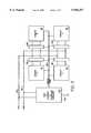
- FIG. 1is a schematic representation of a 256 megabit DRAM designed in accordance with one embodiment of the present invention.
- the DRAMhas eight memory subarrays 10 which are selectively coupled to global signals VCC 50, DVC2 52, GND 60 and VCCP 62.
- DVC2is a voltage source having a potential of approximately one half of VCC, and is often used to bias capacitor plates of the storage cells.
- VCCPis a voltage source greater than one threshold voltage above VCC, and is often used as a source for the word line drivers. Coupling is accomplished via eight isolation circuits 70, one for each subarray 10.
- the control circuit 110in addition to generating standard DRAM timing, interface and control signals, generates eight test and eight repair signals 122 and 124.
- test and repair signalsare combined in each one of eight NOR gates 126 to generate a "DISABLE*" active low isolation control 128 for each of the isolation circuits 70 which correspond to the subarrays 10. It may be desirable to include circuitry that monitors current draw of the device and on power up of the device isolates all subarrays in the event that excessive current is drawn by the device. Then in a test mode, the subarrays are individually enabled in order to determine which are defective. Another option is to include a test pad on the device which during test could be used to input a signal that forces all subarrays to be isolated, and allows individual subarrays to be enabled through the use of test signals.
- REPAIR signals 124may be accomplished with the use of laser fuses, electrically programmable fuses or data stored in a nonvolatile memory location such as a FLASH memory register.
- Methods of generating appropriate repair signals according to these methodscan be accomplished by persons skilled in the art with the aid of the present description.
- Individual subarrayscan be isolated during test or repair, and eight each of local signals 150, 152, 160 and 162 which correspond to a local source of VCC, DVC2, GND and VCCP for each subarray 10 when isolated from the global source signals 50, 52, 60 and 62, respectively, are coupled to the integrated circuit substrate potential 170.
- the subarrays of the DRAMcan be isolated for test or repair purposes either before or after the integrated circuit is packaged depending on the method of generating the repair signals. If the repair signals are generated through the use of laser fuses, it may not be possible to isolate subarrays after the integrated circuit is packaged.
- FIG. 1represents a DRAM where each subarray corresponds to a single input/out data line of the DATA bus 134.
- This architecturelends itself to repair through isolation of a subarray and elimination of an input/output data line. For each defective subarray an input/output data line is dropped, and the remaining input/output data lines are mapped to the functional subarrays. Typically, the data lines will be dropped in order of most significant to least significant for each defective subarray.
- the eighth data linewould be dropped, the sixth data line multiplexed to the seventh subarray.
- the sixth data linecould simply be multiplexed to the eighth subarray. This allows for a consistent device pin out for all devices of a given data width regardless of which subarrays were isolated.
- the data map circuit 180consists of input/output data path multiplexers which are under the control of "DISABLE*" signals 128 and reroute the data input/output lines to the appropriate subarrays 10. Methods of multiplexing data lines are well known in the art and are not specifically described in this specification.
- FIG. 2is a schematic representation of a DRAM which is also designed in accordance with the present invention.
- the DRAMhas memory subarrays 10 which are selectively coupled to global signals VCC 50, DVC2 52, GND 60 and VCCP 62. Coupling is accomplished via isolation circuits 70 to each subarray 10.
- the control circuit 110in addition to generating standard DRAM timing, interface and control functions, generates test signals 122, laser fuse repair signals 124 and electrical fuse repair signals 140. One each of the test and repair signals are combined in each one of logic gates 126 to generate a "DISABLE*" active low isolation control 128 for each of the isolation circuits 70 which correspond to the subarrays 10.
- a three input OR gateis shown to represent the logic function 126; however, numerous other methods of logically combining digital signals are known in the art.
- the DRAM of FIG. 2represents a DRAM where each subarray is tied to multiple input/output data lines of the DATA bus 134.
- This architecturelends itself to repair through isolation of a subarray and elimination of an address line. When a defective subarray is located, half of the subarrays will be electrically isolated from the global signals 50-62, and one address line will be disabled in the address decoder 182. In this particular design the most significant row address is disabled. For example, this technique can provide a 32 megabit DRAM of the same data width as a fully functional 64 megabit DRAM.
- Devices of memory capacity other than 32 megabitscould be obtained through the use of additional address decode modifications and the isolation of fewer or more memory subarrays. If only a single subarray is defective out of eight possible subarrays on a 64 megabit DRAM, it is possible to design the DRAM so that it can be configured as a 56 megabit DRAM.
- the address range corresponding to the defective subarraycan be remapped if necessary so that it becomes the highest address range. In this case, all address lines would be used, but the upper 8 megabits of address space would not be recognized as a valid address for that device, or would be remapped to a functional area of the device.
- Masking an 8 megabit address rangecan be accomplished either through programming of the address decoder or through an address decode/mask function external to the DRAM.
- VCC 50, and GND 60 connectionsare provided to the functional elements through isolation devices 70, 80, 90 and 100.
- the test, control and interface circuit 110provides control and data signals to and from the functional elements via signal bus 120.
- the deviceAfter manufacture, the device is placed in a test mode. Methods of placing a device in a test mode are well known in the art and are not specifically described herein.
- a test modeis provided to electrically isolate one, some or all of the functional elements 12-40 from global supply signals VCC 50 and GND 60 via control signals from 110 over signal bus 120.
- each of the functional elements 12-40allows for the ease of test of the control and interface circuits 110, as well as testing each of the functional elements 12-40 without interference from possible defective elements 12-40. Circuits that are found defective are repaired if possible through the use of redundant elements.
- the redundant elementsmay be located either within the functional blocks 12-40, or elsewhere on the device. After test and repair, any remaining defective functional elements can be programmably isolated from the global supply signals. The device can then be sold in accordance with the functions that are available. Additional signals such as other supply sources, reference signals or control signals may be isolated in addition to global supply signals VCC and GND. Control signals in particular may be isolated by simply isolating the supply signals to the control signal drivers. Further, it may be desirable to couple the local isolated nodes to a reference potential such as the substrate potential when these local nodes are isolated from the global supply, reference or control signals.
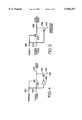
- FIG. 4shows one embodiment of a single isolation circuit of the type that may be used to accomplish the isolation function of elements 70-100 shown in FIGS. 1, 2 and 3.
- One such circuitis required for each signal to be isolated from a functional element such as elements 12-40 of FIG. 3.
- the global signal 410is decoupled from the local signal 420 by the presence of a logic low level on the disable signal node 430 which causes the transistor 440 to become nonconductive between nodes 410 and 420.
- invertor 450causes transistor 460 to conduct between a reference potential 470 and the local node 420.
- the device size of transistor 440will be dependent upon the amount of current it will be required to pass when it is conducting when local node is supplying current to a functioning circuit element. Thus, each such device 440 may have a different device size dependent upon the characteristics of the particular global node 410, and local node 420. It should also be noted that the logic levels associated with the disable signal 430 must be sufficient to allow the desired potential of the global node to pass through the transistor 440 when the local node is not to be isolated from the global node. In the case of an n-channel transistor, the minimum high level of the disable signal will typically be one threshold voltage above the level of the global signal to be passed.
- FIG. 5shows another embodiment of a single isolation circuit of the type that may be used to accomplish the isolation function of elements 70-100 shown in FIGS. 1, 2 and 3.
- One such circuitis required for each signal to be isolated from a functional element such as elements 12-40 of FIG. 3.
- the global signal 510is decoupled from the local signal 520 by the presence of a logic high level on the disable signal node 530 which causes the transistor 540 to become nonconductive between nodes 510 and 520.
- transistor 560conducts between the device substrate potential 570 and the local node 520.
- any current paths between the local node and the substratesuch as may have been caused by a manufacturing defect, will not draw current.
- the disable signal logic levelsshould be chosen such that the low level of the disable signal is a threshold voltage level below the level of the global signal to be passed.
- isolation circuitssuch as those shown in FIGS. 4 and 5 will be used.
- a p-channel isolation devicemay be desirable for passing VCC
- an n-channel isolation devicemay be preferable for passing GND.
- the disable signalmay have ordinary logic swings of VCC to GND. If the global signal is allowed to vary between VCC and GND during operation of the part, then the use of both n-channel and p-channel isolation devices in parallel is desirable with opposite polarities of the disable signal driving the device gates.
- FIG. 6shows an example of a memory module designed in accordance with the teachings of the present invention.
- the memory moduleis a 4 megaword by 36 bit single in line memory module (SIMM) 610.
- the SIMMis made up of six DRAMs 620 of the sixteen megabit DRAM generation organized as 4 Meg ⁇ 4's, and one DRAM 630 of the sixty-four megabit generation organized as 4 Meg ⁇ 12.
- the 4 Meg ⁇ 12 DRAMcontains one or two defective 4 Meg ⁇ 2 arrays of memory elements that are electrically isolated from the remaining circuitry on the DRAM 630.
- the DRAM 630has only a single defective 4 Meg ⁇ 2 array, but a device organization of 4 Meg ⁇ 12 is desired for use in a particular memory module, it may be desirable to terminate unused data input/output lines on the memory module in addition to isolating the defective array. Additionally, it may be determined that it is preferable to isolate a second 4 Meg ⁇ 2 array on the memory device even though it is fully functional in order to provide a lower power 4 Meg ⁇ 12 device. Twenty-four of the data input/output pins on connector 640 are connected to the sixteen megabit DRAMs 620. The remaining twelve data lines are connected to DRAM 630. This SIMM module has numerous advantages over a SIMM module of conventional design using nine 4 M ⁇ 4 DRAMs.
- FIG. 7shows an initialization circuit which when used as part of the present invention allows for automatically isolating defective circuit elements that draw excessive current when an integrated circuit is powered up. By automatically isolating circuit elements that draw excessive current the device can be repaired before it is damaged.
- a power detection circuit 710is used to generate a power-on signal 720 when global supply signal 730 reaches a desired potential.
- Comparator 740is used to compare the potential of global supply 730 with local supply 750. Local supply 750 will be of approximately the same potential as global supply 730 when the isolation device 760 couples 730 to 750 as long as the circuit element 770 is not drawing excessive current.
- circuit element 770does draw excessive current, the resistivity of the isolation device 760 will cause a potential drop in the local supply 750, and the comparator 740 will output a high level on signal 780.
- Power-on signal 720is gated with signal 780 in logic gate 790 so that the comparison is only enabled after power has been on long enough for the local supply potential to reach a valid level. If signals 800 and 810 are both inactive high, then signal 820 from logic gate 790 will pass through gates 830 and 840 and cause isolation signal 850 to be low which will cause the isolation device 760 to decouple the global supply from the local supply. Isolation signal 800 can be used to force signal 850 low regardless of the output of the comparator as long as signal 810 is high.
- Signal 800may be generated from a test mode, or from a programmable source to isolate circuit element 770 for repair or test purposes.
- Test signal 810may be used to force the isolation device 760 to couple the global supply to the local supply regardless of the active high disable signal 860. Signal 810 is useful in testing the device to determine the cause of excessive current draw.
- multiple isolation elementsmay be used for isolation device 760.
- a more resistive isolation deviceis enabled to pass a supply voltage 730 to the circuit 770. If the voltage drop across the resistive device is within a predetermined allowable range, then a second lower resistance isolation device is additionally enabled to pass the supply voltage 730 to circuit 770. This method provides a more sensitive measurement of the current draw of circuit 770.
- the low resistance deviceis not enabled, and the resistive device can optionally be disabled. If the resistive device does not pass enough current to a defective circuit 770, it is not necessary to disable it, or even to design it such that it can be disabled. In this case a simple resistor is adequate.
- FIG. 8is a simplified block diagram representation of a DRAM 800 designed in accordance with another embodiment of the present invention.
- the memory deviceincludes memory cells arranged in eight arrays 802(1)-(8).
- the arrayscan be described as sub-sections of the integrated circuit memory.
- Each arrayhas an associated voltage generator 804(1)-(8) for providing a predetermined voltage level to the arrays.
- a generator control circuit 806is included to provide control signals to the generators to selectively activate or disable the generators.
- Memory operation control circuit 808is included for controlling memory data access operations, and other operations known to those skilled in the art.
- the control circuitreceives operating signals such as RAS*, CAS*, and other known control signals.
- Input/output circuitry 810(I/O)is provided to function as a data buffer for bi-directional data communication with memory controller 816.
- Address circuitry 814addresses the memory arrays in response to address signals provided from the memory controller 816.
- a data map circuitis included to re-route, or map, the data communication lines when one of the arrays is defective, as explained above.
- Generator control circuit 806regulates the operation of generators 804(1)-(8).
- the generator control circuitcan be operated in response to control circuit 808 and detector 818 to selectively turn off the generators to test the memory device for defects.
- the generatorscan be turned off (volatile) to isolate each array from its power supply.
- the generator controlcan be programmed to disable (non-volatile) the voltage generators.
- the generator controlcan be programmed with the use of known programming and repair techniques, such as laser fuses, electrically programmable fuses or data stored in a nonvolatile memory location such as a FLASH memory register.
- individual generators 804can be turned off in a volatile manner during testing. Likewise, individual generators can be disabled in a non-volatile manner during repair.
- the voltage supply to the arrays of the DRAMcan be turned off for test or repair purposes either before or after the integrated circuit is packaged depending on the method of generating the repair signals. If the repair is accomplished through the use of laser fuses, it may not be possible to isolate arrays after the integrated circuit is packaged. If a combination of laser fuses and other techniques such as electrical fuses are used, then repair through isolation may be accomplished either before or after packaging, or both in the event that further device defects become apparent during testing of a repaired packaged device.
- FIG. 8represents a DRAM where each array corresponds to a single input/out data line of the DATA bus which can be coupled for data communication with a memory controller, or microprocessor.
- This architecturelends itself to repair through isolation of an array and elimination of an input/output data line. For each defective array an input/output data line is dropped, and the remaining input/output data lines are mapped to the functional arrays. Typically, the data lines will be dropped in order of most significant to least significant for each defective array. For example, if the array that would otherwise be associated with the sixth of eight input/output data lines is isolated due to defects, the eighth data line would be dropped, the sixth data line multiplexed to the seventh array.
- the sixth data linecould simply be multiplexed to the eighth array. This allows for a consistent device pin out for all devices of a given data width regardless of which arrays were isolated.
- the data map circuit 812consists of input/output data path multiplexers and reroute the data input/output lines to the appropriate arrays 802.
- the memory device of FIG. 8includes memory cells arranged in eight memory arrays. Each memory array has an associated voltage generator circuit 804 for providing a voltage, such as Vcc, Vccp or Vcc/2. Each one of the eight voltage generators can be selectively disabled to turn off the associated array.
- This method of array controlprovides the benefit of flexible fabrication. That is, as integrated circuits become bigger, power distribution becomes more difficult. The requirements of a single voltage generator for an entire circuit would be impractical to meet. Thus, using distributed voltage generators provides a more efficient manner of adjusting an integrated circuit than a series of isolation switches.
- FIG. 9illustrates one embodiment of a voltage generator circuit 806 for providing Vcc/2 to the separate arrays of the memory device.
- the voltage generatorincludes a series of bias pull-up transistors 910 and a series of bias pull-down transistors 912. These transistors are preferably fabricated as long-L transistors.
- Power-on circuitry 914is provided to couple the bias transistors together when the memory RAS* signal is active.
- a control circuit 916is provided which supplies control signals to the gates of p-channel pull-up transistor 918 and n-channel pull-down transistor 919.
- Feed forward lines 924, 926are provided to control n-channel pull-up transistor 928, and p-channel pull-down transistor 930.
- transistors 918, 919, 928, and 930form a voltage divider circuit and are used to interrupt the Vcc/2 voltage supply to a memory array.
- Transistors 918 and 919are normally active in response to control circuit 916.
- the control circuit 916includes a NOR gate 942, first inverter 944, and second inverter 946.
- the NOR gatereceives a Control signal and an inverted Disable signal.
- the output of the NOR gateis coupled to the gates of transistors 918 and 919. Under normal operation, the output of NOR gate 942 is high. Thus, the Control signal is low and the Disable signal is low.
- the Disable signalis used to turn off transistors 918 and 919 and turn on transistors 934 and 936 when an array is defective, and cannot be repaired.
- the disable circuitis preferably controlled using a non-volatile circuit 947, such as a fuse or antifuse which is programmed after fabrication and testing.
- the Control signalis used to selectively interrupt the voltage generator such as during power up or testing.
- the Control signalis a volatile signal which is not dependant upon the detection of a defective array.
- the voltage generator of FIG. 9is one embodiment of a voltage generator which can be incorporated into an integrated circuit so that the integrated circuit can be modified after fabrication to salvage the circuit if defects are discovered. Additional generator circuit designs can be incorporated, as known to those skilled in the art. For example, Vcc or Vccp generators can be provided throughout the memory device to provide a variety of voltage levels to the separate arrays.
- FIG. 10illustrates an alternate embodiment of a voltage generator circuit 1000 to be used as generator 804 in the memory of FIG. 8.
- the generatorincludes an operational amplifier 1002 which receives a reference voltage Vref 1004.
- the amplifierincludes a disable input 1006 for disabling the voltage generator circuit.
- a disable signalcan be provided to the amplifier circuit to interrupt the supply of an output voltage (Vcc) to a memory array.
- a memory circuitwhich includes distributed voltage generators to selectively provide power to memory arrays of the memory circuit.
- Each memory arraycan be turned off if it is determined that the memory array is defective and cannot be repaired. For example, a 256 megabit DRAM with eight arrays could have a number of defective bits that would prevent repair of the device through conventional redundancy techniques.
- memory devices of lower capacityare recovered for sale as 32, 64, 128 megabit or other capacities.
- a 4 megabit by 36 SIMM modulewhich might otherwise be designed with two 4 megabit by 18 DRAMs of the 64 megabit DRAM generation, are designed with three DRAMs where one or more of the DRAMs is manufactured in accordance with the present invention such as three each 4 megabit by 12 DRAMs.
- each of the three DRAMsis of the 64 megabit generation, but each has only 48 megabits of functional memory cells.
- Memory devices of the type described in this specificationcan also be used in multichip modules, single-in-line packages, on motherboards, etc.
- this techniqueis not limited to memory devices such as DRAM, static random access memory (SRAM) and read only memory (ROM, PROM, EPROM, EEPROM, FLASH, etc.).
- a 64 pin programmable logic arraycould take advantage of the disclosed invention to allow partial good die to be sold as 28, 32 or 48 pin logic devices by isolating defective circuitry on the die.
- microprocessorstypically have certain portions of the die that utilize an array of elements such as RAM or ROM as well as a number of integrated discrete functional units. Microprocessors repaired in accordance with the teachings of this invention can be sold as microprocessors with less on board RAM or ROM, or as microprocessors with fewer integrated features.
- a further exampleis of an application specific integrated circuit (ASIC) with multiple circuits that perform independent functions such as an arithmetic unit, a timer, a memory controller, etc. It is possible to isolate defective circuits and obtain functional devices that have a subset of the possible features of a fully functional device. Isolation of defective circuits may be accomplished through the use of laser fuses, electrical fuses, other nonvolatile data storage elements, or the programming of control signals. Electrical fuses include circuits which are normally conductive and are programmably opened, and circuits which are normally open and are programmably closed such as anti-fuses.
- One advantage of this inventionis that it provides an integrated circuit that can be tested and repaired despite the presence of what would previously have been catastrophic defects. Another advantage of this invention is that it provides an integrated circuit that does not exhibit undesirable electrical characteristics due to the presence of defective elements.
- the DRAMis partitioned into multiple arrays which can be electrically isolated from other circuitry on the DRAM. Additionally, the DRAM has test circuitry 819 which is used to individually activate and deactivate each of the memory arrays as needed to identify defective arrays. The DRAM also has programmable elements 806 which allow for the electrical isolation of defective arrays to be permanent at least with respect to the end user of the DRAM. After the DRAM is manufactured, it is tested to verify functionality. If the device is nonfunctional, individual memory arrays, or groups of arrays may be electrically isolated from the remaining DRAM circuitry. Upon further tests, it may be discovered that one or more memory arrays are defective, and that these defects result in the overall nonfunctionality of the DRAM. The DRAM is then programmed to isolate the known defective arrays and their associated circuitry. The DRAM data path is also programmed in accordance with the desired device organization.
- a memory circuithas been described which includes distributed voltage generators to selectively provide power to memory arrays of the memory circuit.
- Each memory arraycan be turned off if it is determined that the memory array is defective and cannot be repaired.
- the memory devicetherefore, can be salvaged by reducing the operational capacity of the memory device.
Landscapes
- Engineering & Computer Science (AREA)
- Power Engineering (AREA)
- Dram (AREA)
- For Increasing The Reliability Of Semiconductor Memories (AREA)
- Techniques For Improving Reliability Of Storages (AREA)
- Semiconductor Integrated Circuits (AREA)
- Amplifiers (AREA)
- Transmitters (AREA)
Abstract
Description
Claims (24)
Priority Applications (10)
| Application Number | Priority Date | Filing Date | Title |
|---|---|---|---|
| US08/918,637US5946257A (en) | 1996-07-24 | 1997-08-22 | Selective power distribution circuit for an integrated circuit |
| JP2000508115AJP2001514428A (en) | 1997-08-22 | 1998-08-24 | Selective power distribution circuit for integrated circuits. |
| AU91172/98AAU9117298A (en) | 1997-08-22 | 1998-08-24 | Selective power distribution circuit for an integrated circuit |
| EP98943351AEP1019910B1 (en) | 1997-08-22 | 1998-08-24 | Selective power distribution circuit for an integrated circuit |
| DE69808956TDE69808956T2 (en) | 1997-08-22 | 1998-08-24 | PARTIAL DISABLED POWER SUPPLY FOR INTEGRATED CIRCUITS |
| PCT/US1998/017512WO1999010891A1 (en) | 1997-08-22 | 1998-08-24 | Selective power distribution circuit for an integrated circuit |
| KR1020007001797AKR100358670B1 (en) | 1997-08-22 | 1998-08-24 | Selective power distribution circuit for an integrated circuit |
| AT98943351TATE226752T1 (en) | 1997-08-22 | 1998-08-24 | PARTIALLY DISCONNECTABLE POWER SUPPLY FOR INTEGRATED CIRCUITS |
| US09/304,299US6078540A (en) | 1996-07-24 | 1999-05-03 | Selective power distribution circuit for an integrated circuit |
| US09/597,393US6356498B1 (en) | 1996-07-24 | 2000-06-19 | Selective power distribution circuit for an integrated circuit |
Applications Claiming Priority (2)
| Application Number | Priority Date | Filing Date | Title |
|---|---|---|---|
| US08/685,783US5761145A (en) | 1994-10-19 | 1996-07-24 | Efficient method for obtaining usable parts from a partially good memory integrated circuit |
| US08/918,637US5946257A (en) | 1996-07-24 | 1997-08-22 | Selective power distribution circuit for an integrated circuit |
Related Parent Applications (1)
| Application Number | Title | Priority Date | Filing Date |
|---|---|---|---|
| US08/685,783Continuation-In-PartUS5761145A (en) | 1994-10-19 | 1996-07-24 | Efficient method for obtaining usable parts from a partially good memory integrated circuit |
Related Child Applications (1)
| Application Number | Title | Priority Date | Filing Date |
|---|---|---|---|
| US09/304,299ContinuationUS6078540A (en) | 1996-07-24 | 1999-05-03 | Selective power distribution circuit for an integrated circuit |
Publications (1)
| Publication Number | Publication Date |
|---|---|
| US5946257Atrue US5946257A (en) | 1999-08-31 |
Family
ID=25440710
Family Applications (3)
| Application Number | Title | Priority Date | Filing Date |
|---|---|---|---|
| US08/918,637Expired - LifetimeUS5946257A (en) | 1996-07-24 | 1997-08-22 | Selective power distribution circuit for an integrated circuit |
| US09/304,299Expired - LifetimeUS6078540A (en) | 1996-07-24 | 1999-05-03 | Selective power distribution circuit for an integrated circuit |
| US09/597,393Expired - LifetimeUS6356498B1 (en) | 1996-07-24 | 2000-06-19 | Selective power distribution circuit for an integrated circuit |
Family Applications After (2)
| Application Number | Title | Priority Date | Filing Date |
|---|---|---|---|
| US09/304,299Expired - LifetimeUS6078540A (en) | 1996-07-24 | 1999-05-03 | Selective power distribution circuit for an integrated circuit |
| US09/597,393Expired - LifetimeUS6356498B1 (en) | 1996-07-24 | 2000-06-19 | Selective power distribution circuit for an integrated circuit |
Country Status (8)
| Country | Link |
|---|---|
| US (3) | US5946257A (en) |
| EP (1) | EP1019910B1 (en) |
| JP (1) | JP2001514428A (en) |
| KR (1) | KR100358670B1 (en) |
| AT (1) | ATE226752T1 (en) |
| AU (1) | AU9117298A (en) |
| DE (1) | DE69808956T2 (en) |
| WO (1) | WO1999010891A1 (en) |
Cited By (33)
| Publication number | Priority date | Publication date | Assignee | Title |
|---|---|---|---|---|
| US6078540A (en)* | 1996-07-24 | 2000-06-20 | Micron Technology, Inc. | Selective power distribution circuit for an integrated circuit |
| US6094395A (en)* | 1998-03-27 | 2000-07-25 | Infineon Technologies North America Corp. | Arrangement for controlling voltage generators in multi-voltage generator chips such as DRAMs |
| US6097647A (en)* | 1994-10-19 | 2000-08-01 | Micron Technology, Inc. | Efficient method for obtaining usable parts from a partially good memory integrated circuit |
| US6496421B1 (en) | 2000-08-31 | 2002-12-17 | Micron Technology, Inc. | Distributed cell plate and/or digit equilibrate voltage generator |
| US20020192846A1 (en)* | 2001-06-13 | 2002-12-19 | Samsung Electronics Co., Ltd. | Control signal transmitting method with package power pin and related integrated circuit package structure |
| US20030059046A1 (en)* | 2001-07-20 | 2003-03-27 | Stmicroelectronics S.R.I. | Hybrid architecture for realizing a random numbers generator |
| WO2003063170A1 (en)* | 2002-01-25 | 2003-07-31 | Infineon Technologies Ag | Circuit for deactivating faulty functional components |
| US20040136257A1 (en)* | 2003-01-10 | 2004-07-15 | International Business Machines Corporation | Method and System For Merging Multiple Fuse Decompression Serial Bitstreams To Support Auxiliary Fuseblow Capability |
| US20050015654A1 (en)* | 2003-06-24 | 2005-01-20 | Micron Technology, Inc. | Circuits and methods for repairing defects in memory devices |
| US7057866B2 (en)* | 2001-08-14 | 2006-06-06 | International Business Machines Corp. | System and method for disconnecting a portion of an integrated circuit |
| US7098689B1 (en)* | 2003-09-19 | 2006-08-29 | Xilinx, Inc. | Disabling unused/inactive resources in programmable logic devices for static power reduction |
| US20070165461A1 (en)* | 2006-01-18 | 2007-07-19 | Cornwell Michael J | Disabling faulty flash memory dies |
| US7345944B1 (en) | 2006-01-11 | 2008-03-18 | Xilinx, Inc. | Programmable detection of power failure in an integrated circuit |
| US20080291760A1 (en)* | 2007-05-23 | 2008-11-27 | Micron Technology, Inc. | Sub-array architecture memory devices and related systems and methods |
| US20080304341A1 (en)* | 2007-06-11 | 2008-12-11 | Hynix Semiconductor Inc. | Redundancy circuit |
| US7498839B1 (en) | 2004-10-22 | 2009-03-03 | Xilinx, Inc. | Low power zones for programmable logic devices |
| US7498836B1 (en) | 2003-09-19 | 2009-03-03 | Xilinx, Inc. | Programmable low power modes for embedded memory blocks |
| US7498835B1 (en) | 2005-11-04 | 2009-03-03 | Xilinx, Inc. | Implementation of low power standby modes for integrated circuits |
| US7504854B1 (en)* | 2003-09-19 | 2009-03-17 | Xilinx, Inc. | Regulating unused/inactive resources in programmable logic devices for static power reduction |
| US7549139B1 (en) | 2003-09-19 | 2009-06-16 | Xilinx, Inc. | Tuning programmable logic devices for low-power design implementation |
| US7581124B1 (en) | 2003-09-19 | 2009-08-25 | Xilinx, Inc. | Method and mechanism for controlling power consumption of an integrated circuit |
| US20090323418A1 (en)* | 2006-05-15 | 2009-12-31 | Cornwell Michael J | Use of Alternative Value in Cell Detection |
| US20100070798A1 (en)* | 2006-05-15 | 2010-03-18 | Apple Inc. | Maintenance Operations for Multi-Level Data Storage Cells |
| US20100157674A1 (en)* | 2006-05-15 | 2010-06-24 | Apple Inc. | Two Levels of Voltage Regulation Supplied for Logic and Data Programming Voltage of a Memory Device |
| US20110007539A1 (en)* | 2006-06-22 | 2011-01-13 | Micron Technology, Inc. | Test mode for multi-chip integrated circuit packages |
| US20110170348A1 (en)* | 2006-05-15 | 2011-07-14 | Apple Inc. | Analog interface for a flash memory die |
| US20110242894A1 (en)* | 2010-04-06 | 2011-10-06 | Vogan Andrew W | Method and system to isolate memory modules in a solid state drive |
| US8462550B2 (en) | 2006-05-15 | 2013-06-11 | Apple Inc. | Off-die charge pump that supplies multiple flash devices |
| US8823405B1 (en) | 2010-09-10 | 2014-09-02 | Xilinx, Inc. | Integrated circuit with power gating |
| US20230121581A1 (en)* | 2021-10-14 | 2023-04-20 | Samsung Electronics Co., Ltd. | Variable resistance memory device |
| US20240071437A1 (en)* | 2022-08-30 | 2024-02-29 | Micron Technology, Inc. | Die Disablement |
| CN117897673A (en)* | 2021-08-25 | 2024-04-16 | 苹果公司 | Scalable hierarchical power transmission system |
| US12399648B2 (en) | 2022-09-06 | 2025-08-26 | Micron Technology, Inc. | Die-based rank management |
Families Citing this family (21)
| Publication number | Priority date | Publication date | Assignee | Title |
|---|---|---|---|---|
| US6421810B1 (en)* | 1999-05-05 | 2002-07-16 | National Semiconductor Corporation | Scalable parallel test bus and testing method |
| DE19924153B4 (en)* | 1999-05-26 | 2006-02-09 | Infineon Technologies Ag | Circuit arrangement for repair of a semiconductor memory |
| US6563339B2 (en)* | 2001-01-31 | 2003-05-13 | Micron Technology, Inc. | Multiple voltage supply switch |
| US6525982B1 (en)* | 2001-09-11 | 2003-02-25 | Micron Technology, Inc. | Methods of programming and circuitry for a programmable element |
| US6704228B2 (en)* | 2001-12-28 | 2004-03-09 | Samsung Electronics Co., Ltd | Semiconductor memory device post-repair circuit and method |
| US7779285B2 (en)* | 2003-02-18 | 2010-08-17 | Oracle America, Inc. | Memory system including independent isolated power for each memory module |
| DE60325576D1 (en)* | 2003-07-16 | 2009-02-12 | St Microelectronics Srl | Redundancy scheme for an integrated memory module |
| KR100670700B1 (en)* | 2004-10-30 | 2007-01-17 | 주식회사 하이닉스반도체 | Delay fixed loop power supply circuit |
| DE102005015319B4 (en)* | 2005-04-01 | 2008-04-10 | Infineon Technologies Ag | Electrical system with faulty memory areas and method for testing memory areas |
| US7624318B2 (en)* | 2005-09-27 | 2009-11-24 | International Business Machines Corporation | Method and apparatus for automatically identifying multiple combinations of operational and non-operational components on integrated circuit chips with a single part number |
| KR100647473B1 (en)* | 2005-11-16 | 2006-11-23 | 삼성전자주식회사 | Multi-chip package semiconductor device and defect detection method |
| CA2541046A1 (en)* | 2006-03-27 | 2007-09-27 | Mosaid Technologies Incorporated | Power supply testing architecture |
| KR100784869B1 (en) | 2006-06-26 | 2007-12-14 | 삼성전자주식회사 | Memory system to reduce quiescent current |
| JP4967532B2 (en)* | 2006-08-25 | 2012-07-04 | 富士通セミコンダクター株式会社 | Semiconductor integrated circuit and test method for semiconductor integrated circuit |
| KR100802060B1 (en)* | 2007-02-02 | 2008-02-11 | 삼성전자주식회사 | Semiconductor memory device and test method thereof for preventing excessive application of specific stress items |
| WO2008117383A1 (en)* | 2007-03-23 | 2008-10-02 | Fujitsu Limited | Electronic device, electronic apparatus mounting electronic device, article mounting electronic device, and method for manufacturing electronic device |
| US20100128447A1 (en)* | 2008-11-21 | 2010-05-27 | Tyco Electronics Corporation | Memory module having voltage regulator module |
| US8526252B2 (en)* | 2009-03-17 | 2013-09-03 | Seagate Technology Llc | Quiescent testing of non-volatile memory array |
| WO2013003029A2 (en) | 2011-06-29 | 2013-01-03 | Rambus Inc. | Multi-element memory device with power control for individual elements |
| EP2907134B1 (en) | 2012-10-12 | 2020-06-10 | Thomas Andre | Memory device with reduced on-chip noise |
| US10446532B2 (en) | 2016-01-13 | 2019-10-15 | Invensas Bonding Technologies, Inc. | Systems and methods for efficient transfer of semiconductor elements |
Citations (24)
| Publication number | Priority date | Publication date | Assignee | Title |
|---|---|---|---|---|
| US3762037A (en)* | 1971-03-30 | 1973-10-02 | Ibm | Method of testing for the operability of integrated semiconductor circuits having a plurality of separable circuits |
| EP0283186A2 (en)* | 1987-03-06 | 1988-09-21 | Kabushiki Kaisha Toshiba | Semiconductor integrated circuit with a plurality of circuit blocks having equivalent functions |
| US4799193A (en)* | 1985-10-09 | 1989-01-17 | Kabushiki Kaisha Toshiba | Semiconductor memory devices |
| US4992984A (en)* | 1989-12-28 | 1991-02-12 | International Business Machines Corporation | Memory module utilizing partially defective memory chips |
| US5025344A (en)* | 1988-11-30 | 1991-06-18 | Carnegie Mellon University | Built-in current testing of integrated circuits |
| EP0451595A2 (en)* | 1990-04-10 | 1991-10-16 | National Semiconductor Corporation | Short circuit detector circuit for memory array |
| US5134584A (en)* | 1988-07-22 | 1992-07-28 | Vtc Incorporated | Reconfigurable memory |
| US5235548A (en)* | 1989-04-13 | 1993-08-10 | Dallas Semiconductor Corp. | Memory with power supply intercept in redundancy logic |
| US5235550A (en)* | 1991-05-16 | 1993-08-10 | Micron Technology, Inc. | Method for maintaining optimum biasing voltage and standby current levels in a DRAM array having repaired row-to-column shorts |
| US5255234A (en)* | 1990-12-22 | 1993-10-19 | Samsung Electronics Co., Ltd. | Redundant means of a semiconductor memory device and method thereof |
| US5262993A (en)* | 1990-11-16 | 1993-11-16 | Hitachi, Ltd. | Semiconductor memory having redundancy circuit with means to switch power from a normal memory block to a spare memory block |
| US5295101A (en)* | 1992-01-31 | 1994-03-15 | Texas Instruments Incorporated | Array block level redundancy with steering logic |
| US5349559A (en)* | 1991-08-19 | 1994-09-20 | Samsung Electronics Co., Ltd. | Internal voltage generating circuit |
| US5384727A (en)* | 1993-11-08 | 1995-01-24 | Advanced Micro Devices, Inc. | Fuse trimming in plastic package devices |
| US5396465A (en)* | 1992-11-24 | 1995-03-07 | Samsung Electronics Co., Ltd. | Circuit for controlling isolation transistors in a semiconductor memory device |
| US5400281A (en)* | 1991-06-27 | 1995-03-21 | Nec Corporation | Static random access memory device with memory cell testing circuit |
| US5406520A (en)* | 1991-08-30 | 1995-04-11 | Texas Instruments Incorporated | Universal modular memory |
| US5412601A (en)* | 1992-08-31 | 1995-05-02 | Nippon Steel Corporation | Non-volatile semiconductor memory device capable of storing multi-value data in each memory cell |
| US5424989A (en)* | 1992-08-21 | 1995-06-13 | Kabushiki Kaisha Toshiba | Semiconductor memory device |
| US5428575A (en)* | 1992-08-28 | 1995-06-27 | Mitsubishi Denki Kabushiki Kaisha | Semiconductor memory device with comparing circuit for facilitating test mode |
| US5615162A (en)* | 1995-01-04 | 1997-03-25 | Texas Instruments Incorporated | Selective power to memory |
| US5673232A (en)* | 1994-07-18 | 1997-09-30 | Mitsubishi Denki Kabushiki Kaisha | Semiconductor memory device operating stably under low power supply voltage with low power consumption |
| US5761145A (en)* | 1994-10-19 | 1998-06-02 | Micron Technology, Inc. | Efficient method for obtaining usable parts from a partially good memory integrated circuit |
| US5787044A (en)* | 1995-10-23 | 1998-07-28 | Micron Technology, Inc. | Memory-cell array and a method for repairing the same |
Family Cites Families (9)
| Publication number | Priority date | Publication date | Assignee | Title |
|---|---|---|---|---|
| US3750116A (en) | 1972-06-30 | 1973-07-31 | Ibm | Half good chip with low power dissipation |
| EP0480915B1 (en) | 1985-08-20 | 1995-11-22 | STMicroelectronics, Inc. | Defective element disabling circuit having a laser-blown fuse |
| US4829481A (en) | 1985-08-20 | 1989-05-09 | Sgs-Thomson Microelectronics, Inc. | Defective element disabling circuit having a laser-blown fuse |
| KR880006704A (en) | 1986-11-03 | 1988-07-23 | 앤 오 · 바스킨스 | Self test and self repair memory system and its manufacture and use method |
| US4939694A (en) | 1986-11-03 | 1990-07-03 | Hewlett-Packard Company | Defect tolerant self-testing self-repairing memory system |
| JPS63164100A (en) | 1986-12-26 | 1988-07-07 | Hiroshi Nakamura | Semiconductor integrated circuit memory |
| JPH07153296A (en)* | 1993-11-26 | 1995-06-16 | Nec Corp | Semiconductor memory |
| US5901105A (en)* | 1995-04-05 | 1999-05-04 | Ong; Adrian E | Dynamic random access memory having decoding circuitry for partial memory blocks |
| US5946257A (en)* | 1996-07-24 | 1999-08-31 | Micron Technology, Inc. | Selective power distribution circuit for an integrated circuit |
- 1997
- 1997-08-22USUS08/918,637patent/US5946257A/ennot_activeExpired - Lifetime
- 1998
- 1998-08-24JPJP2000508115Apatent/JP2001514428A/enactivePending
- 1998-08-24ATAT98943351Tpatent/ATE226752T1/ennot_activeIP Right Cessation
- 1998-08-24EPEP98943351Apatent/EP1019910B1/ennot_activeExpired - Lifetime
- 1998-08-24AUAU91172/98Apatent/AU9117298A/ennot_activeAbandoned
- 1998-08-24KRKR1020007001797Apatent/KR100358670B1/ennot_activeExpired - Fee Related
- 1998-08-24DEDE69808956Tpatent/DE69808956T2/ennot_activeExpired - Lifetime
- 1998-08-24WOPCT/US1998/017512patent/WO1999010891A1/enactiveIP Right Grant
- 1999
- 1999-05-03USUS09/304,299patent/US6078540A/ennot_activeExpired - Lifetime
- 2000
- 2000-06-19USUS09/597,393patent/US6356498B1/ennot_activeExpired - Lifetime
Patent Citations (25)
| Publication number | Priority date | Publication date | Assignee | Title |
|---|---|---|---|---|
| US3762037A (en)* | 1971-03-30 | 1973-10-02 | Ibm | Method of testing for the operability of integrated semiconductor circuits having a plurality of separable circuits |
| US4799193A (en)* | 1985-10-09 | 1989-01-17 | Kabushiki Kaisha Toshiba | Semiconductor memory devices |
| EP0283186A2 (en)* | 1987-03-06 | 1988-09-21 | Kabushiki Kaisha Toshiba | Semiconductor integrated circuit with a plurality of circuit blocks having equivalent functions |
| US5134584A (en)* | 1988-07-22 | 1992-07-28 | Vtc Incorporated | Reconfigurable memory |
| US5025344A (en)* | 1988-11-30 | 1991-06-18 | Carnegie Mellon University | Built-in current testing of integrated circuits |
| US5235548A (en)* | 1989-04-13 | 1993-08-10 | Dallas Semiconductor Corp. | Memory with power supply intercept in redundancy logic |
| US4992984A (en)* | 1989-12-28 | 1991-02-12 | International Business Machines Corporation | Memory module utilizing partially defective memory chips |
| EP0451595A2 (en)* | 1990-04-10 | 1991-10-16 | National Semiconductor Corporation | Short circuit detector circuit for memory array |
| US5262993A (en)* | 1990-11-16 | 1993-11-16 | Hitachi, Ltd. | Semiconductor memory having redundancy circuit with means to switch power from a normal memory block to a spare memory block |
| US5255234A (en)* | 1990-12-22 | 1993-10-19 | Samsung Electronics Co., Ltd. | Redundant means of a semiconductor memory device and method thereof |
| US5235550A (en)* | 1991-05-16 | 1993-08-10 | Micron Technology, Inc. | Method for maintaining optimum biasing voltage and standby current levels in a DRAM array having repaired row-to-column shorts |
| US5400281A (en)* | 1991-06-27 | 1995-03-21 | Nec Corporation | Static random access memory device with memory cell testing circuit |
| US5349559A (en)* | 1991-08-19 | 1994-09-20 | Samsung Electronics Co., Ltd. | Internal voltage generating circuit |
| US5406520A (en)* | 1991-08-30 | 1995-04-11 | Texas Instruments Incorporated | Universal modular memory |
| US5295101A (en)* | 1992-01-31 | 1994-03-15 | Texas Instruments Incorporated | Array block level redundancy with steering logic |
| US5424989A (en)* | 1992-08-21 | 1995-06-13 | Kabushiki Kaisha Toshiba | Semiconductor memory device |
| US5428575A (en)* | 1992-08-28 | 1995-06-27 | Mitsubishi Denki Kabushiki Kaisha | Semiconductor memory device with comparing circuit for facilitating test mode |
| US5412601A (en)* | 1992-08-31 | 1995-05-02 | Nippon Steel Corporation | Non-volatile semiconductor memory device capable of storing multi-value data in each memory cell |
| US5396465A (en)* | 1992-11-24 | 1995-03-07 | Samsung Electronics Co., Ltd. | Circuit for controlling isolation transistors in a semiconductor memory device |
| US5384727A (en)* | 1993-11-08 | 1995-01-24 | Advanced Micro Devices, Inc. | Fuse trimming in plastic package devices |
| US5412594A (en)* | 1993-11-08 | 1995-05-02 | Advanced Micro Devices, Inc. | Fuse trimming in plastic package devices |
| US5673232A (en)* | 1994-07-18 | 1997-09-30 | Mitsubishi Denki Kabushiki Kaisha | Semiconductor memory device operating stably under low power supply voltage with low power consumption |
| US5761145A (en)* | 1994-10-19 | 1998-06-02 | Micron Technology, Inc. | Efficient method for obtaining usable parts from a partially good memory integrated circuit |
| US5615162A (en)* | 1995-01-04 | 1997-03-25 | Texas Instruments Incorporated | Selective power to memory |
| US5787044A (en)* | 1995-10-23 | 1998-07-28 | Micron Technology, Inc. | Memory-cell array and a method for repairing the same |
Non-Patent Citations (2)
| Title |
|---|
| Kitsukawa, G., et al., "WP 3.4: 256Mb DRAM Technologies for File Applications", 1993 IEEE International Solid-State Circuit Conf., 48,49,261, (1993). |
| Kitsukawa, G., et al., WP 3.4: 256Mb DRAM Technologies for File Applications , 1993 IEEE International Solid State Circuit Conf., 48,49,261, (1993).* |
Cited By (66)
| Publication number | Priority date | Publication date | Assignee | Title |
|---|---|---|---|---|
| US6097647A (en)* | 1994-10-19 | 2000-08-01 | Micron Technology, Inc. | Efficient method for obtaining usable parts from a partially good memory integrated circuit |
| US6356498B1 (en)* | 1996-07-24 | 2002-03-12 | Micron Technology, Inc. | Selective power distribution circuit for an integrated circuit |
| US6078540A (en)* | 1996-07-24 | 2000-06-20 | Micron Technology, Inc. | Selective power distribution circuit for an integrated circuit |
| US6094395A (en)* | 1998-03-27 | 2000-07-25 | Infineon Technologies North America Corp. | Arrangement for controlling voltage generators in multi-voltage generator chips such as DRAMs |
| US6700824B2 (en) | 2000-08-31 | 2004-03-02 | Micron Technology, Inc. | Distributed cell plate and/or digit equilibrate voltage generator |
| US6496421B1 (en) | 2000-08-31 | 2002-12-17 | Micron Technology, Inc. | Distributed cell plate and/or digit equilibrate voltage generator |
| US20020192846A1 (en)* | 2001-06-13 | 2002-12-19 | Samsung Electronics Co., Ltd. | Control signal transmitting method with package power pin and related integrated circuit package structure |
| US6815230B2 (en)* | 2001-06-13 | 2004-11-09 | Samsung Electronics Co., Ltd. | Control signal transmitting method with package power pin and related integrated circuit package structure |
| US20030059046A1 (en)* | 2001-07-20 | 2003-03-27 | Stmicroelectronics S.R.I. | Hybrid architecture for realizing a random numbers generator |
| US7139397B2 (en)* | 2001-07-20 | 2006-11-21 | Stmicroelectronics S.R.L. | Hybrid architecture for realizing a random numbers generator |
| US7057866B2 (en)* | 2001-08-14 | 2006-06-06 | International Business Machines Corp. | System and method for disconnecting a portion of an integrated circuit |
| WO2003063170A1 (en)* | 2002-01-25 | 2003-07-31 | Infineon Technologies Ag | Circuit for deactivating faulty functional components |
| US20040136257A1 (en)* | 2003-01-10 | 2004-07-15 | International Business Machines Corporation | Method and System For Merging Multiple Fuse Decompression Serial Bitstreams To Support Auxiliary Fuseblow Capability |
| US6856569B2 (en)* | 2003-01-10 | 2005-02-15 | International Business Machines Corporation | Method and system for merging multiple fuse decompression serial bitstreams to support auxiliary fuseblow capability |
| US7437632B2 (en) | 2003-06-24 | 2008-10-14 | Micron Technology, Inc. | Circuits and methods for repairing defects in memory devices |
| US7836362B2 (en) | 2003-06-24 | 2010-11-16 | Micron Technology, Inc. | Circuits and methods for repairing defects in memory devices |
| US20050015654A1 (en)* | 2003-06-24 | 2005-01-20 | Micron Technology, Inc. | Circuits and methods for repairing defects in memory devices |
| US20070168771A1 (en)* | 2003-06-24 | 2007-07-19 | Micron Technology, Inc. | Circuits and methods for repairing defects in memory devices |
| US20070168772A1 (en)* | 2003-06-24 | 2007-07-19 | Micron Technology, Inc. | Circuits and methods for repairing defects in memory devices |
| US7873882B2 (en) | 2003-06-24 | 2011-01-18 | Micron Technology, Inc. | Circuits and methods for repairing defects in memory devices |
| US7581124B1 (en) | 2003-09-19 | 2009-08-25 | Xilinx, Inc. | Method and mechanism for controlling power consumption of an integrated circuit |
| US7098689B1 (en)* | 2003-09-19 | 2006-08-29 | Xilinx, Inc. | Disabling unused/inactive resources in programmable logic devices for static power reduction |
| US8099691B1 (en) | 2003-09-19 | 2012-01-17 | Xilinx, Inc. | Disabling unused/inactive resources in an integrated circuit for static power reduction |
| US7498836B1 (en) | 2003-09-19 | 2009-03-03 | Xilinx, Inc. | Programmable low power modes for embedded memory blocks |
| US7504854B1 (en)* | 2003-09-19 | 2009-03-17 | Xilinx, Inc. | Regulating unused/inactive resources in programmable logic devices for static power reduction |
| US7549139B1 (en) | 2003-09-19 | 2009-06-16 | Xilinx, Inc. | Tuning programmable logic devices for low-power design implementation |
| US7562332B1 (en) | 2003-09-19 | 2009-07-14 | Xilinx, Inc. | Disabling unused/inactive resources in programmable logic devices for static power reduction |
| US7498839B1 (en) | 2004-10-22 | 2009-03-03 | Xilinx, Inc. | Low power zones for programmable logic devices |
| US7498835B1 (en) | 2005-11-04 | 2009-03-03 | Xilinx, Inc. | Implementation of low power standby modes for integrated circuits |
| US7345944B1 (en) | 2006-01-11 | 2008-03-18 | Xilinx, Inc. | Programmable detection of power failure in an integrated circuit |
| US7609561B2 (en) | 2006-01-18 | 2009-10-27 | Apple Inc. | Disabling faulty flash memory dies |
| EP2224451A1 (en)* | 2006-01-18 | 2010-09-01 | Apple Inc. | Disabling faulty flash memory dies |
| US20070165461A1 (en)* | 2006-01-18 | 2007-07-19 | Cornwell Michael J | Disabling faulty flash memory dies |
| US8055959B2 (en) | 2006-01-18 | 2011-11-08 | Apple Inc. | Disabling faulty flash memory dies |
| US20100002512A1 (en)* | 2006-01-18 | 2010-01-07 | Cornwell Michael J | Disabling faulty flash memory dies |
| EP1811525A3 (en)* | 2006-01-18 | 2007-09-12 | Apple Computer, Inc. | Disabling faulty flash memory dies |
| CN101004953B (en)* | 2006-01-18 | 2010-09-08 | 苹果公司 | Disable faulty flash memory chips |
| US20100157674A1 (en)* | 2006-05-15 | 2010-06-24 | Apple Inc. | Two Levels of Voltage Regulation Supplied for Logic and Data Programming Voltage of a Memory Device |
| US8116133B2 (en) | 2006-05-15 | 2012-02-14 | Apple Inc. | Maintenance operations for multi-level data storage cells |
| US9042170B2 (en) | 2006-05-15 | 2015-05-26 | Apple Inc. | Off-die charge pump that supplies multiple flash devices |
| US8462550B2 (en) | 2006-05-15 | 2013-06-11 | Apple Inc. | Off-die charge pump that supplies multiple flash devices |
| US20100070798A1 (en)* | 2006-05-15 | 2010-03-18 | Apple Inc. | Maintenance Operations for Multi-Level Data Storage Cells |
| US20110170348A1 (en)* | 2006-05-15 | 2011-07-14 | Apple Inc. | Analog interface for a flash memory die |
| US8964469B2 (en) | 2006-05-15 | 2015-02-24 | Apple Inc. | Off-die charge pump that supplies multiple flash devices |
| US20090323418A1 (en)* | 2006-05-15 | 2009-12-31 | Cornwell Michael J | Use of Alternative Value in Cell Detection |
| US9245616B2 (en) | 2006-05-15 | 2016-01-26 | Apple Inc. | Dynamic cell state resolution |
| US8830747B2 (en) | 2006-05-15 | 2014-09-09 | Apple Inc. | Off-die charge pump that supplies multiple flash devices |
| US8127202B2 (en) | 2006-05-15 | 2012-02-28 | Apple Inc. | Use of alternative value in cell detection |
| US8356231B2 (en) | 2006-05-15 | 2013-01-15 | Apple Inc. | Use of alternative value in cell detection |
| KR101133897B1 (en)* | 2006-05-15 | 2012-04-09 | 애플 인크. | Maintenance operations for multi-level data storage cells |
| US8159897B2 (en) | 2006-05-15 | 2012-04-17 | Apple Inc. | Two levels of voltage regulation supplied for logic and data programming voltage of a memory device |
| US8355284B2 (en) | 2006-05-15 | 2013-01-15 | Apple Inc. | Analog interface for a flash memory die |
| US8136000B2 (en)* | 2006-06-22 | 2012-03-13 | Micron Technology, Inc. | Test mode for multi-chip integrated circuit packages |
| US20110007539A1 (en)* | 2006-06-22 | 2011-01-13 | Micron Technology, Inc. | Test mode for multi-chip integrated circuit packages |
| US20080291760A1 (en)* | 2007-05-23 | 2008-11-27 | Micron Technology, Inc. | Sub-array architecture memory devices and related systems and methods |
| US7573763B2 (en)* | 2007-06-11 | 2009-08-11 | Hynix Semiconductor Inc. | Redundancy circuit |
| US20080304341A1 (en)* | 2007-06-11 | 2008-12-11 | Hynix Semiconductor Inc. | Redundancy circuit |
| US8705281B2 (en)* | 2010-04-06 | 2014-04-22 | Intel Corporation | Method and system to isolate memory modules in a solid state drive |
| US20110242894A1 (en)* | 2010-04-06 | 2011-10-06 | Vogan Andrew W | Method and system to isolate memory modules in a solid state drive |
| US8823405B1 (en) | 2010-09-10 | 2014-09-02 | Xilinx, Inc. | Integrated circuit with power gating |
| CN117897673A (en)* | 2021-08-25 | 2024-04-16 | 苹果公司 | Scalable hierarchical power transmission system |
| US12346179B2 (en) | 2021-08-25 | 2025-07-01 | Apple Inc. | Scalable, hierarchical power delivery system |
| US20230121581A1 (en)* | 2021-10-14 | 2023-04-20 | Samsung Electronics Co., Ltd. | Variable resistance memory device |
| US20240071437A1 (en)* | 2022-08-30 | 2024-02-29 | Micron Technology, Inc. | Die Disablement |
| US12300351B2 (en)* | 2022-08-30 | 2025-05-13 | Micron Technology, Inc. | Die disablement |
| US12399648B2 (en) | 2022-09-06 | 2025-08-26 | Micron Technology, Inc. | Die-based rank management |
Also Published As
| Publication number | Publication date |
|---|---|
| DE69808956T2 (en) | 2003-09-11 |
| EP1019910A1 (en) | 2000-07-19 |
| US6078540A (en) | 2000-06-20 |
| US6356498B1 (en) | 2002-03-12 |
| ATE226752T1 (en) | 2002-11-15 |
| KR100358670B1 (en) | 2002-10-31 |
| KR20010023171A (en) | 2001-03-26 |
| WO1999010891A1 (en) | 1999-03-04 |
| JP2001514428A (en) | 2001-09-11 |
| DE69808956D1 (en) | 2002-11-28 |
| EP1019910B1 (en) | 2002-10-23 |
| AU9117298A (en) | 1999-03-16 |
Similar Documents
| Publication | Publication Date | Title |
|---|---|---|
| US5946257A (en) | Selective power distribution circuit for an integrated circuit | |
| US5761145A (en) | Efficient method for obtaining usable parts from a partially good memory integrated circuit | |
| US5153880A (en) | Field-programmable redundancy apparatus for memory arrays | |
| EP0034070B1 (en) | Fault tolerant memory system | |
| US5838625A (en) | Anti-fuse programming path | |
| US5161157A (en) | Field-programmable redundancy apparatus for memory arrays | |
| US4860260A (en) | Semiconductor memory device with testing of redundant memory cells | |
| US6324106B2 (en) | Semiconductor memory device capable of recovering defective bit and a system having the same semiconductor memory device | |
| US4459685A (en) | Redundancy system for high speed, wide-word semiconductor memories | |
| EP0637036B1 (en) | Redundancy element check in IC memory without programming substitution of redundant elements | |
| EP0657811B1 (en) | Integrated circuitry for checking the utilization rate of redundancy memory elements in a semiconductor memory device | |
| US7107467B2 (en) | Semiconductor memory device having a circuit for removing noise from a power line of the memory device using a plurality of decoupling capactors | |
| US6208570B1 (en) | Redundancy test method for a semiconductor memory | |
| US6552937B2 (en) | Memory device having programmable column segmentation to increase flexibility in bit repair | |
| US6930934B2 (en) | High efficiency redundancy architecture in SRAM compiler | |
| US5708601A (en) | Integrated circuitry for checking the utilization rate of redundancy memory elements in a semiconductor memory device | |
| US6535436B2 (en) | Redundant circuit and method for replacing defective memory cells in a memory device | |
| KR100274105B1 (en) | Memory chip structure and package method for increased production | |
| JP2009531668A (en) | Power supply test architecture | |
| US6717869B2 (en) | Integrated circuit having redundant, self-organized architecture for improving yield | |
| KR20020064014A (en) | Semiconductor memory device with burn-in test function | |
| WO1990012401A1 (en) | Memory with power supply intercept and redundancy logic | |
| KR20050087012A (en) | Semiconductor memory device having a cell-power monitoring mean | |
| KR19980036479A (en) | Partial fault relief device in memory |
Legal Events
| Date | Code | Title | Description |
|---|---|---|---|
| AS | Assignment | Owner name:MICRON TECHNOLOGY, INC., IDAHO Free format text:ASSIGNMENT OF ASSIGNORS INTEREST;ASSIGNOR:KEETH, BRENT;REEL/FRAME:008697/0309 Effective date:19970801 | |
| STCF | Information on status: patent grant | Free format text:PATENTED CASE | |
| FPAY | Fee payment | Year of fee payment:4 | |
| FPAY | Fee payment | Year of fee payment:8 | |
| FPAY | Fee payment | Year of fee payment:12 | |
| AS | Assignment | Owner name:U.S. BANK NATIONAL ASSOCIATION, AS COLLATERAL AGENT, CALIFORNIA Free format text:SECURITY INTEREST;ASSIGNOR:MICRON TECHNOLOGY, INC.;REEL/FRAME:038669/0001 Effective date:20160426 Owner name:U.S. BANK NATIONAL ASSOCIATION, AS COLLATERAL AGEN Free format text:SECURITY INTEREST;ASSIGNOR:MICRON TECHNOLOGY, INC.;REEL/FRAME:038669/0001 Effective date:20160426 | |
| AS | Assignment | Owner name:MORGAN STANLEY SENIOR FUNDING, INC., AS COLLATERAL AGENT, MARYLAND Free format text:PATENT SECURITY AGREEMENT;ASSIGNOR:MICRON TECHNOLOGY, INC.;REEL/FRAME:038954/0001 Effective date:20160426 Owner name:MORGAN STANLEY SENIOR FUNDING, INC., AS COLLATERAL Free format text:PATENT SECURITY AGREEMENT;ASSIGNOR:MICRON TECHNOLOGY, INC.;REEL/FRAME:038954/0001 Effective date:20160426 | |
| AS | Assignment | Owner name:U.S. BANK NATIONAL ASSOCIATION, AS COLLATERAL AGENT, CALIFORNIA Free format text:CORRECTIVE ASSIGNMENT TO CORRECT THE REPLACE ERRONEOUSLY FILED PATENT #7358718 WITH THE CORRECT PATENT #7358178 PREVIOUSLY RECORDED ON REEL 038669 FRAME 0001. ASSIGNOR(S) HEREBY CONFIRMS THE SECURITY INTEREST;ASSIGNOR:MICRON TECHNOLOGY, INC.;REEL/FRAME:043079/0001 Effective date:20160426 Owner name:U.S. BANK NATIONAL ASSOCIATION, AS COLLATERAL AGEN Free format text:CORRECTIVE ASSIGNMENT TO CORRECT THE REPLACE ERRONEOUSLY FILED PATENT #7358718 WITH THE CORRECT PATENT #7358178 PREVIOUSLY RECORDED ON REEL 038669 FRAME 0001. ASSIGNOR(S) HEREBY CONFIRMS THE SECURITY INTEREST;ASSIGNOR:MICRON TECHNOLOGY, INC.;REEL/FRAME:043079/0001 Effective date:20160426 | |
| AS | Assignment | Owner name:MICRON TECHNOLOGY, INC., IDAHO Free format text:RELEASE BY SECURED PARTY;ASSIGNOR:U.S. BANK NATIONAL ASSOCIATION, AS COLLATERAL AGENT;REEL/FRAME:047243/0001 Effective date:20180629 | |
| AS | Assignment | Owner name:MICRON TECHNOLOGY, INC., IDAHO Free format text:RELEASE BY SECURED PARTY;ASSIGNOR:MORGAN STANLEY SENIOR FUNDING, INC., AS COLLATERAL AGENT;REEL/FRAME:050937/0001 Effective date:20190731 |