US5945707A - DRAM cell with grooved transfer device - Google Patents
DRAM cell with grooved transfer deviceDownload PDFInfo
- Publication number
- US5945707A US5945707AUS09/056,903US5690398AUS5945707AUS 5945707 AUS5945707 AUS 5945707AUS 5690398 AUS5690398 AUS 5690398AUS 5945707 AUS5945707 AUS 5945707A
- Authority
- US
- United States
- Prior art keywords
- groove
- gate
- channel
- semiconductor device
- regions
- Prior art date
- Legal status (The legal status is an assumption and is not a legal conclusion. Google has not performed a legal analysis and makes no representation as to the accuracy of the status listed.)
- Expired - Lifetime
Links
- 238000012546transferMethods0.000titledescription9
- 239000000758substrateSubstances0.000claimsdescription28
- 239000004065semiconductorSubstances0.000claimsdescription21
- 239000003990capacitorSubstances0.000claimsdescription18
- 238000003860storageMethods0.000claimsdescription11
- 238000002955isolationMethods0.000claimsdescription10
- 238000000034methodMethods0.000abstractdescription25
- 239000004020conductorSubstances0.000abstractdescription15
- 150000004767nitridesChemical class0.000description46
- 229910021420polycrystalline siliconInorganic materials0.000description33
- 229920005591polysiliconPolymers0.000description33
- 125000006850spacer groupChemical group0.000description23
- XUIMIQQOPSSXEZ-UHFFFAOYSA-NSiliconChemical compound[Si]XUIMIQQOPSSXEZ-UHFFFAOYSA-N0.000description11
- 238000005530etchingMethods0.000description11
- 229910052710siliconInorganic materials0.000description11
- 239000010703siliconSubstances0.000description11
- 239000000463materialSubstances0.000description8
- 229920000642polymerPolymers0.000description7
- 239000012535impuritySubstances0.000description6
- 238000005229chemical vapour depositionMethods0.000description5
- 238000009792diffusion processMethods0.000description5
- 239000012212insulatorSubstances0.000description5
- 238000004519manufacturing processMethods0.000description5
- 230000014759maintenance of locationEffects0.000description4
- 238000012545processingMethods0.000description4
- WQJQOUPTWCFRMM-UHFFFAOYSA-Ntungsten disilicideChemical compound[Si]#[W]#[Si]WQJQOUPTWCFRMM-UHFFFAOYSA-N0.000description4
- 229910021342tungsten silicideInorganic materials0.000description4
- 230000015572biosynthetic processEffects0.000description3
- 239000002019doping agentSubstances0.000description3
- 238000001459lithographyMethods0.000description3
- 239000000126substanceSubstances0.000description3
- VYPSYNLAJGMNEJ-UHFFFAOYSA-NSilicium dioxideChemical compoundO=[Si]=OVYPSYNLAJGMNEJ-UHFFFAOYSA-N0.000description2
- 230000003247decreasing effectEffects0.000description2
- 230000005669field effectEffects0.000description2
- 238000000059patterningMethods0.000description2
- 238000005498polishingMethods0.000description2
- 229910052814silicon oxideInorganic materials0.000description2
- WFKWXMTUELFFGS-UHFFFAOYSA-NtungstenChemical compound[W]WFKWXMTUELFFGS-UHFFFAOYSA-N0.000description2
- 229910052721tungstenInorganic materials0.000description2
- 239000010937tungstenSubstances0.000description2
- 238000003491arrayMethods0.000description1
- 230000004888barrier functionEffects0.000description1
- 230000015556catabolic processEffects0.000description1
- 230000007547defectEffects0.000description1
- 238000006731degradation reactionMethods0.000description1
- 238000000151depositionMethods0.000description1
- 230000008021depositionEffects0.000description1
- 230000000694effectsEffects0.000description1
- 230000005684electric fieldEffects0.000description1
- 238000010894electron beam technologyMethods0.000description1
- 238000002513implantationMethods0.000description1
- 238000011065in-situ storageMethods0.000description1
- 230000003647oxidationEffects0.000description1
- 238000007254oxidation reactionMethods0.000description1
- 238000012856packingMethods0.000description1
- 230000035515penetrationEffects0.000description1
- 230000010363phase shiftEffects0.000description1
- 238000000206photolithographyMethods0.000description1
- 229920002120photoresistant polymerPolymers0.000description1
- 229920000052poly(p-xylylene)Polymers0.000description1
Images


Classifications
- H—ELECTRICITY
- H10—SEMICONDUCTOR DEVICES; ELECTRIC SOLID-STATE DEVICES NOT OTHERWISE PROVIDED FOR
- H10B—ELECTRONIC MEMORY DEVICES
- H10B12/00—Dynamic random access memory [DRAM] devices
- H10B12/01—Manufacture or treatment
- H10B12/02—Manufacture or treatment for one transistor one-capacitor [1T-1C] memory cells
- H10B12/05—Making the transistor
- H10B12/053—Making the transistor the transistor being at least partially in a trench in the substrate
- H—ELECTRICITY
- H10—SEMICONDUCTOR DEVICES; ELECTRIC SOLID-STATE DEVICES NOT OTHERWISE PROVIDED FOR
- H10D—INORGANIC ELECTRIC SEMICONDUCTOR DEVICES
- H10D84/00—Integrated devices formed in or on semiconductor substrates that comprise only semiconducting layers, e.g. on Si wafers or on GaAs-on-Si wafers
- H—ELECTRICITY
- H10—SEMICONDUCTOR DEVICES; ELECTRIC SOLID-STATE DEVICES NOT OTHERWISE PROVIDED FOR
- H10B—ELECTRONIC MEMORY DEVICES
- H10B12/00—Dynamic random access memory [DRAM] devices
- H10B12/01—Manufacture or treatment
- H10B12/02—Manufacture or treatment for one transistor one-capacitor [1T-1C] memory cells
- H10B12/03—Making the capacitor or connections thereto
- H10B12/038—Making the capacitor or connections thereto the capacitor being in a trench in the substrate
- H—ELECTRICITY
- H10—SEMICONDUCTOR DEVICES; ELECTRIC SOLID-STATE DEVICES NOT OTHERWISE PROVIDED FOR
- H10B—ELECTRONIC MEMORY DEVICES
- H10B12/00—Dynamic random access memory [DRAM] devices
- H10B12/30—DRAM devices comprising one-transistor - one-capacitor [1T-1C] memory cells
- H10B12/48—Data lines or contacts therefor
- H10B12/488—Word lines
Definitions
- the present inventionis directed to a semiconductor memory cell having a grooved planar transfer device, and methods for making thereof, and more particularly, to a DRAM (dynamic random access memory) cell having an increased channel length resulting from the groove.
- DRAMdynamic random access memory
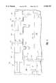
- FIG. 1shows a schematic of a typical DRAM cell 100 having a field effect transistor (FET) 105 and a storage capacitor C S .
- the gate of the FET 105acts as the wordline W/L.
- a bitline B/Lis connected to one terminal of the FET 105, which terminal is the source or drain of the DRAM, depending on the application, such as read and write operations.
- the other DRAM terminalis connected to a strap or storage node 110 of the storage capacitor C S .
- the other terminal of the storage capacitor C Sis referred to as a plate 115.
- the cell sizeis minimized by scaling lithographic features F.
- Fis the minimum linewidth of the feature size that can be patterned with lithography. Accordingly, if a minimum cell size is to be obtained, it is necessary to reduce the size of the transistor 105 of FIG. 1 as much as possible. This reduces the gate channel length. However, shorter gate channel lengths increase leakage currents between the storage node 110 and bitline B/L to unacceptable levels. The reduced gate channel lengths degrade subthreshold leakage, and hence the retention time. Subthreshold leakage may be reduced by increasing the channel doping concentration. However, this increases and degrades junction leakage, which also reduces retention time.
- the object of the present inventionis to provide a memory cell array, and a method of making thereof, that eliminate the problems of conventional memory cell arrays.
- Another object of the present inventionis to provide a memory cell having an increased channel length without increasing the cell area.
- a further object of the present inventionis to provide a memory cell array, and a method of making thereof, where the memory cell has source and drain regions that are self-aligned to the gate without increasing the cell area.
- Yet another object of the present inventionis to provide a memory cell array, and a method of making thereof, where the memory cell has a groove which may or may not be self-aligned under the word line.
- An additional object of the present inventionis to provide a memory cell having a high density without detrimentally increasing leakage current and decreasing retention time.
- a semiconductor device and a method of making thereofwhich includes a memory cell having a grooved gate formed in a sub-lithographic groove.
- the grooveextends the channel length to include the groove sidewalls and width of the groove.
- Each sidewall section, or the sum of the two sidewall sections, of the channel located along the gate sidewallshas a larger length than the length of the bottom channel section located along the gate bottom.
- the memory deviceis primarily controlled by the sidewall channel sections, instead of the bottom channel section.
- the grooveis etched into the substrate through an opening formed by patterning a resist using lithographic or sub-lithographic methods.
- the opening widthis further reduced by forming spacers on the opening's sidewalls.
- the groovemay be self-aligned, i.e., centered along the width of the gate conductor.
- the gateextends over the substrate beyond the groove width, and the source and drain regions are self-aligned to the gate.
- the source and drain regionsare implanted prior or after forming the groove.
- the grooveis a stepped groove formed by a two step etch to further increase the channel length.
- FIG. 1shows a schematic of a conventional DRAM cell
- FIG. 2shows a cross section of a memory cell according to the present invention
- FIG. 3is top view of a layout of an array of several of the memory cells shown in FIG. 2 according to the present invention
- FIGS. 4-6show a method of forming the memory cell of FIG. 2 according to the present invention
- FIGS. 7-8show another method of forming the memory cell of FIG. 2 according to the present invention.
- FIGS. 9-11show yet another method of forming the memory cell of FIG. 2 according to the present invention.
- FIGS. 12-14show a method of forming a stepped groove according to another embodiment of the present invention.
- FIGS. 15-19show another method of forming a memory cell according to yet another embodiment of the present invention.
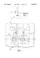
- FIG. 2shows a cross section of a memory cell 200 according to one embodiment of the present invention.
- the memory cellincludes a semiconductor device, such as a field effect transistor (FET), formed in a substrate 205 doped with P-type material, for example, having a P-well 210 formed therein.
- FETfield effect transistor
- the capacitor plate 115also shown in FIG. 1, is formed in the substrate 205 by forming an N + region 115 in the substrate 205.
- a deep trench (DT)is etched into the substrate 205 and the storage capacitor plate 115 is formed by outdiffusing N + dopant from the DT sidewalls.
- Node dielectric 212is formed and the deep trench (DT) is filled with doped polysilicon.
- the polysiliconis recessed, and an insulating collar 215 is formed on the top sidewall portions of the deep trench DT, which is then filled with doped polysilicon 217. Note, the insulating collar 215 is excluded from an upper part 219 of one of the top DT sidewall portions in order to out-diffuse a strap 110 from the DT polysilicon 217.
- the DT polysilicon 217is recessed again to expose parts of the collar 215, which is silicon oxide for example.
- the exposed collaris etched and the recess is filled again with polysilicon 217, from which the strap 110 is out-diffused to connect the DT polysilicon 217 to the source/drain of the transfer device 202.
- the storage node 110 of the capacitoris the source or drain region of a FET 202 formed in the P-well 210.
- a shallow trench isolation regions STI 400covers a portion of the deep trench DT.
- the FET 202has a grooved gate 225 formed in a groove 230, which is formed in the P-well 210 between the source and drain N + regions 110, 235 of the FET 202.
- the grooved gate 225extends beyond the groove 230 over the substrate, and the source or drain regions 110, 235 are self-aligned to the gate 225, for example.
- the source or drain regions 110, 235are heavily doped N + regions in the P-well 210.
- the groove 230may be self aligned to be at the center of the gate 225, for example. Alternatively, the groove 225 is not self-aligned, and may be anywhere below gate 225.
- a thin layer of gate oxide 240separates the gate 225 from the FET channel in the P-well 210.
- the groove 230extends the width of the FET channel as described below and shown as reference numeral 325 in FIG. 3.
- the groove 230also extends the length of the FET channel to include sidewalls and bottom width of the groove 230, which channel length is shown as reference numerals 255, 265, 260 in FIG. 2.
- the groove 230is separated from the source/drain N + regions 110, 235 so that the channel length is increased to include lateral distances 245, 250, shown in FIG. 2.
- the gate 225is formed of polysilicon, which may be doped with either N + or P + impurities, and acts as the wordline W/L (also shown in FIG. 1) of the memory cell 200. In this embodiment, portions of the gate 225 extend over the P-well 210. This extends the gate 225 beyond the groove 230 to control the resistance of the FET channel, which is located in the P-well 210 between the source/drain N + regions 110, 235.
- the groove 230 and grooved gate 225extend the length of the channel to include the distances 245, 250 between the groove 230 and the source/drain N + regions 110, 235, the distances 255, 260 of the groove sidewalls, and the bottom width 265 of the groove 230.
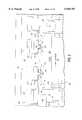
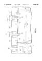
- FIG. 3is top view of a layout of an array 300 of several of the memory cells 200, where FIG. 2 is a cross section of the layout shown in FIG. 3 along the line 2-2'.
- FIG. 3also shows exposed strips 320 used to form the grooves 230, which are only formed in the active regions AA by selective etching the silicon substrate to the surrounding insulating layer.
- the width of the gate formed in the groove 230is shown in FIG. 3 as reference numeral 325.
- the grooves 230are formed by patterning a mask 330 (shown in FIG. 4) to cover areas other than the exposed strips 320.
- the shallow trench isolation regions STI shown in FIG. 2surround the active regions AA, shown in FIG. 3.
- an insulating layer 283covers the portion of the active regions AA that overlaps the deep trench DT.
- FIG. 3also shows the deep trenches DT as well as the bit line contacts CB, which are also shown in FIG. 2 as reference numeral 285.
- a shallow trench isolation region (STI) 400is formed in the substrate, e.g., over portions of the deep trench DT, to isolated the FET 202 from other devices formed in the substrate.
- the STI regions 400, the top covers 283 of the deep trenches DTs, and the collars 215are oxides of silicon.
- the depth of the STI regions 400is greater than a depth of the groove 230. This fully isolates the memory cell 200 from other adjacent devices, such as other memory cells that form an array of memory cells, as shown by reference numeral 300 in FIG. 3. Having STI regions 400 that are deeper than the groove 230 reduces leakage of charges stored in the deep trench capacitor C S when the FET 202 is in the OFF state. Otherwise, large leakage occurs which detrimentally degrades the performance of the memory cell 200 and prevents its use as a DRAM cell.
- isolation region STIis less than a depth of the groove 230, then leakage is particularly pronounced at the ends 310, 315 of the groove 230, shown in FIG. 3. Thus, having isolation regions STI that are deeper then the groove depth, minimizes leakage, including leakage at the groove ends 310, 315.
- a gate contact or wiring layer 270also referred to as a gate conductor, such as a tungsten W or a tungsten silicide WSi x layer for example, is formed over the gate 225.
- the gate 225 and gate wiring 270have a width that equals a minimum lithographic feature size F. Accordingly, the width of the groove 230 located below a portion of the gate 225 is less than the feature size F.
- An insulator or dielectric 275such as a nitride, is formed to cover the gate wiring 270 and sidewalls of the gate 225.
- An oxide layer 280is formed over the memory cell 200 and is etched selectively to the insulator 275 to form a bit line contact opening that exposes the source and drain N + region 235 located furthest from the deep trench DT.
- the opening over the exposed N + region 235is filled with a conductive material to form the bit line contact 285 borderlessly to the word-line or gate 225.
- a bit-line 290is formed over the oxide layer 280 to connect various bit line contacts 285 arranged in rows of the array 300, shown in FIG. 3, formed from many of the memory cells 200 arranged in rows and columns.
- the source and drain regions 110, 235are located along the length 325 of groove 230 and the channel is located in the P-well 210 along the lateral, sidewalls and bottom portions of the gate 225.
- the length of the channelis the sum of the lateral distances 245, 250 between the source/drain regions 10, 235, the distances 255, 260 of the sidewalls of the groove 230, equaling approximately twice the depth of the groove 230, and the width 265 of the groove 230.
- the gate 225may be confined within the groove 230, and the source/drain regions 110, 235 abut the groove 230. In this case, the length of the channel is approximately the distances 255, 260 of the groove sidewalls plus the groove bottom width 265.
- the width of the channelis approximately the length 325 of the groove 230. Accordingly, as shown in FIG. 2, the channel sidewall sections located along the gate sidewall portions 255, 260, each or together, have a larger length than the length of the bottom channel section located along the gate bottom portion 265. If desired, the groove 230 may be deeper so that each sidewall length 255 or 260 is greater than the bottom width 265. Having larger sidewalls sections than a bottom section allows the gate sidewall portions 255, 260 (FIG. 2) to predominantly control the memory cell 200.
- conventional grooved deviceshave the predominant portion of the channel at the bottom of a grooved gate, as opposed to the sidewalls of the groove, and are controlled by the bottom portion of the grooved gate or channel, instead of the sidewalls portions thereof.
- Controlling the FET or memory cell by the grooved gate's sidewallsprovides substantial benefits, such as increased channel length, improved shielding from penetration of drain electric field to the source, referred to as drain induced barrier lowering (DIBL), and a threshold voltage which is independent of the dimension of the groove, particularly the width of the groove.
- DIBLdrain induced barrier lowering
- V t of the MOSFET arraythe doping in the channel may be reduced, thus avoiding degradation, i.e., increase, of junction leakage due to high doping effects.
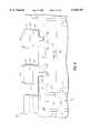
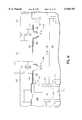
- FIGS. 4-6show one method of fabricating the memory cell 200.
- a mask 330is formed over the substrate that includes therein the shallow trench isolation (STI) regions formed over portions of the deep trench capacitor C S .
- STIshallow trench isolation
- the deep trench DTis etched into substrate 205 (or the P-well 210) and the storage capacitor plate 115 is formed by outdiffusing N + dopant from the deep trench DT sidewalls.
- the node dielectric 212is formed and the deep trench DT is filled with doped polysilicon.
- the polysiliconis recessed and the insulating collar 215 is formed on the sidewalls of the deep trench DT, which is then filled with doped polysilicon 217.
- This polysilicon 217is also recessed, to expose part of the collar 215, which is oxides of silicon for example.
- the exposed collar oxide 215is etched, and the recess filled again with polysilicon which is used to form, e.g. out-diffuse, the strap 110 between the deep trench DT and the source/drain of the transfer device 202.
- the shallow trench isolation (STI) regionsare formed and planarized (e.g., by chemical polish).
- the hybrid resist mask 330is applied, exposed, baked and developed to form sub-lithographic strips 335 having a width of approximately 0.45 F.
- the mask 330includes alternating strips of positive and negative hybrid resist separated by the sub-lithographic space of approximately 0.45 F to form the exposed strips 335.
- the mask 330is formed over an oxide layer 340 which is formed over the P-well 210 between the STI regions 400.
- phase-shift lithographymay be used instead of the hybrid resist.
- a spacer 350 of approximately 0.08 Fis conformally formed over the structure shown in FIG. 4.
- the spacer 350is a polymer spacer and is deposited in an etching chamber to narrow the groove opening to approximately 0.3 F and form the exposed strips 320, also shown in FIG. 3.
- the silicon (of the active region AA shown in FIG. 3)which is exposed through the strips 320, is etched to form the groove 230 into the P-well 210.
- the groove 230is etched selectively to oxide after removing the polymer spacer material 350 and portions of the oxide layer 340 located at the bottom of the strips 320. Referring to FIG. 3, areas of the cell array other than the active regions AA are covered by oxide. Accordingly, after forming the strips 320, etching silicon selective to oxide forms the grooves 230 only in the silicon of the active regions AA exposed through the strips 320.
- the grooves 230are formed using, for example, X-ray, electron beam or other shorter-wave optical lithography. If desired or necessary, for example, to optimize the characteristic of the transfer device or FET 202, the bottom channel portion 355 located below the bottom of the groove is doped, e.g., implanted with impurities.
- the hybrid resist 330 and spacer 350are removed. If necessary, a sacrificial oxide layer is grown and etched off to remove any surface damaged by the groove etching. Next, a gate oxide layer 240 is grown to cover the bottom and sidewalls of the groove 230.
- the gate 225is formed using conventional photo-lithographic methods. For example, a film of gate conductor material, such as doped polysilicon and tungsten silicide WSi x formed on the doped polysilicon, is deposited over the wafer substrate, patterned lithographically to define a masked line over the etched groove structure, and subtractively etched to form a gate stack or gate conductor, that includes the doped polysilicon gate 225 and tungsten silicide WSi x gate wiring 270.
- the gate stackencompasses the groove 230, where the doped polysilicon gate 225 is formed in the groove 230 and over portions of the substrate adjacent to the groove 230.
- a nitride cap 275can be included over the gate conductor stack to serve as isolation material for the borderless bit line contacts 285, for example.
- the groove 230is not necessarily centered in the middle of the gate 225. That is, the gate 225 and gate wiring 270 are not self-aligned to the groove 230.
- N + regions 110, 235are implanted and diffused as necessary, and a nitride spacer 277 is formed over sidewalls of the nitride cap 275, gate wiring conductor 270, and the gate 225. Finally, returning to FIG. 2, the oxide layer 280, bit line contact 285 and bit line 290 are formed.
- FIGS. 7 and 8show an alternate method of forming the sub-lithographic grooves 230.
- an insulating layer 370such as a nitride layer, is formed over the oxide layer 340 that covers the P-well 210 between the STI regions 400.
- the alternating strips of positive and negative hybrid resist mask 330are applied over the STI regions 400 and the nitride layer 370.
- the hybrid resist mask 330is exposed, baked, developed and the nitride 370 is etched to form the sub-lithographic strips 335 having a width of 0.45 F.
- the hybrid resist 330is removed and a spacer 380, such as a nitride spacer, having a width of approximately 0.08 F, is formed over the sidewalls of the nitride layer 370.
- the spacers 380 located over the sidewalls of the nitride layer 370narrow the groove opening 335 from approximately 0.45 F to approximately 0.3 F and form the strips 320.
- siliconis etched selectively to oxide and nitride after etching through the oxide 340 located at the bottom of the strips 320. This forms the groove 230 into the P-well 210. After the groove 230 is formed by etching, a thin oxide layer is grown to protect the exposed silicon at the bottom of the groove 230 during a subsequent nitride strip.
- the nitride spacer and layer 380, 370are removed.
- the remaining stepsare identical to those described in connection with FIG. 6, where the gate oxide 240, the gate 225, gate wiring 270 and nitride cover 275, as well as the N + source/drain regions 110, 235, are formed.
- the memory cell 200 shown in FIG. 1is completed by forming the top oxide layer 280, the bit line contact 285, and the bit line 290. Similar to the first method, this second method which uses the nitride layer 370 also results in a gate 225 and gate wiring 270 which are not self-aligned to the groove 230. That is, the groove 230 is not necessarily centered in the middle of the gate 225.
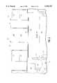
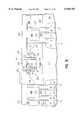
- FIGS. 9-11show another method according to another embodiment, where the groove 230 is self-aligned to the gate 225.
- This methodincludes a combination of sub-lithographic and Damascene word-line process steps to create the sub-lithographic sized and self-aligned groove 230 under the gate 225 of the transfer device 202 (FIG. 2).
- Damascene word-line processrefers to etching trenches in an insulator layer, such as an oxide layer, and filling the trenches with a gate conductor to form the word-line in the trenches. Excess gate conductor formed outside the trenches are removed, e.g., using chemical mechanical polishing (CMP).
- CMPchemical mechanical polishing
- the Damascene wordline processis in contrast to another method of forming word-lines, where the gate conductor is blanket deposited on the insulator layer and patterned with a subtractive etch, as described in connection with FIG. 6, to form the word-lines.
- the deep trench capacitor C S , the N + capacitor plate 115, the P-well 210, and the STI regions 400are formed in the substrate using steps which are identical to that described in connection with FIG. 4.
- a thin nitride liner 410is formed, e.g. deposited, over the substrate.
- the nitride liner 410acts as an etch stop during subsequent etching.
- a thick oxide layer 420is formed, e.g. deposited, over the nitride etch stop 410.
- the oxide layer 420is etched to expose portions 425 of the nitride etch stop 410 using photo-lithographic steps, such as forming a photo resist mask 430 over the oxide layer 420.
- the mask 430is patterned to expose portions of the oxide layer 420, which portions are etched to expose the portions 425 of the nitride etch stop 410.
- the exposed portions 425 of the nitride etch stop 410have a width of 1 F, where F is the minimum lithographic feature size.
- nitride spacers 440are formed on the sidewalls of the oxide layer 420.
- the nitride spacer 440has a thickness of approximately 0.35 F and forms the groove strips 320, shown in FIGS. 3 and 10, having a width of approximately 0.3 F.
- the groove 230is etched selectively to nitride and oxide into the silicon of the P-well 210, which is in the active area AA shown in FIG. 3.
- the nitride spacer 440is removed and, as shown in FIG. 11, the gate oxide 240 is formed to cover the sidewalls and bottom of the groove 230, similar to that described in connection with FIG. 6.
- the portion of the channel in the P-well 210 located at bottom of the groove(shown in FIG. 6 as reference numeral 355) is implanted to improve the performance of the FET 202.
- a sacrificial oxide layeris grown and stripped prior to forming the gate oxide 240. The reason for the sacrificial oxide layer is to remove any silicon surface defects created by prior processing steps.
- the gate stack shown in FIG. 2 and 6is formed.
- intrinsic polysiliconis deposited in the opening 425 (FIG. 9) formed in the oxide layer 420, which opening has a width of 1 F after removal of the nitride spacers 440 (FIG. 10).
- the polysilicon 225is planarized and recessed below the top surface of the oxide layer 420.
- the recessed intrinsic polysiliconis implanted with impurities to dope the intrinsic polysilicon and form the gate 225.
- in-situ doped polysiliconmay be used.
- the gate wiring 270is deposited over the gate polysilicon 225 and planarized to the top surface of the oxide layer 420. Thereafter, the planarized WSi x or W layer 270 is recessed to form the gate wiring 270.
- the gate wiring 270is made of tungsten silicide (WSi x ) or tungsten (W).
- a thick nitride layer 275is deposited and planarized to form the nitride cap 275.
- the oxide layer 420 and nitride liner 410are etched off and the structure shown in FIG. 6 is formed by implanting and diffusing impurities in the P-well 210 to form the N + source/drain regions 110, 235.
- the nitride spacer 277is formed on sidewalls of the nitride cap 275, gate wiring conductor 270, and the gate 225.
- the nitride sidewallsare formed by a blanket nitride deposition, which is then etched and removed except for the nitride at the sidewalls of the nitride cap 275, gate wiring conductor 270, and the gate 225.
- the oxide layer 280, borderless bit line contact 285 and bitline 290are formed.
- a stepped groove(shown in FIG. 14 as reference numeral 490) may be formed instead of the groove 230 shown in the previous figures.
- a stack of dielectric layershaving a nitride 410 and oxide 420 layers, and a photo-resist mask layer 430 (FIG. 9), are formed over the substrate that includes the deep trench capacitor CS and STI regions 400.
- the oxide layer 420is patterned and etched, as described above using a patterned mask, for example, to expose portions 450 of the substrate. This is similar to that shown in FIG. 9, where the width of the exposed portion 450 is one lithographic feature size F.
- the opening 450is exposed using conventional lithography to pattern the Damascene gate structure in the oxide layer 420, using the resist mask 430 (FIG. 9) which is exposed and developed, and the resist pattern is etched to remove portions of the oxide layer 420.
- a first spacer forming materialsuch as nitride, is deposited and anisotropically etched to form nitride spacers 470 on sidewalls of the oxide layer 420 for narrowing the width of the first openings 450 to result in second openings 485 (FIG. 13).
- second spacer forming materialpreferably polymer spacer forming material such as parylene
- second spacer forming materialis deposited and anisotropically etched to form polymer spacers 475 on sidewalls of the nitride spacer 470 for further narrowing the second openings 485 to result in third openings 480, shown in FIGS. 12 and 13.
- the thicknesses of the two deposited spacer forming materialsare chosen such that the nitride and polymer spacers 470, 475 have a desired width, so that the widths of the successively narrower openings 480, 485 (FIG. 13) are the desired dimension of the groove 490 to be formed in the substrate or P-well 210.
- the first groove 480is etched into the P-well 210, using the combination of the oxide 420, nitride spacers 470, polymer spacers 475 and STI oxide 400 as an etching mask.
- the polymer spacers 475are removed, and the exposed silicon substrate is etched into the P-well 210, using the combination of oxide 420, nitride spacers 470, and STI oxide 400 as the etching mask. This transfers the wider portion of the groove 485 into the P-well 210, while the narrow portion of the groove 480 is further etched deeper into the P-well 210 to form a stepped groove 490.
- the nitride spacers 470 and oxide layer 340are removed to expose the wide opening 450 (FIG. 12).
- the remaining steps that form the gate stack structure shown in FIG. 14, as well as further steps to complete the device structure,are identical to those described in connection with FIG. 11 and, for brevity, will not be repeated.
- Forming the stepped groove using the above described methodprovides the stepped groove structure 490 which is easier to fill with polysilicon. Further, the stepped groove 490 provides formation of a narrower and deeper groove gate so that the effective channel length is further increased. Multiple spacers, i.e, more than the two spacers 470, 475 (FIG. 12) described above, may be used to make a stepped groove having multiple steps to eliminate polysilicon filling problems for a narrow and deep groove gate formation.
- a memory cellis formed having a grooved Damascene gate with pre-formed source/drain diffusion regions.
- FIG. 15shows a cross section of a memory cell processed up to the formation of the P-well 210 and an N + doped layer 500 where, as previously described, an N + capacitor plate 115 is formed and deep trench processing performed to form the deep trench capacitor C S in the deep trench DT.
- the deep trench DTis lined with node dielectric layers 212.
- the upper portion of the deep trench DTis lined with the oxide collar 215.
- the deep trench DTis filled with polysilicon 217.
- the oxide collar 215does not line the top portion of the deep trench DT to leave the unlined portion 219 so that the buried strap 110 (FIGS. 2, 18) to be formed contacts the polysilicon 217 in the deep trench DT.
- the STI regions 400are formed. Thereafter, impurities are implanted in the substrate 205 to form the P-well 210 similar to that described in connection with FIG. 4.
- impuritiesare implanted or diffused in the P-well 210 to form a heavily doped N + layer 500 in the P-well 210 prior to forming the groove and gate.
- This heavily doped N + layer 500will be used to later form the source/drain regions 110, 235 of the FET 202, shown in FIG. 2.
- a thin nitride etch stop layer 410is formed over the entire structure, i.e., over the heavily doped N + layer 500, the deep trench DT, and the STI regions 400.
- a silicon oxide layer 420is formed over the nitride layer 410.
- the nitride and oxide layers 410, 420are formed by chemical vapor deposition (CVD).
- a conventional photo-resist mask 430is applied over the oxide layer 420. Similar to FIG. 9, the mask 430 is patterned, exposed and etched to expose portions 425 of the nitride liner 410, which portions 425 have a width of 1 F of more, for example.
- the mask 430is removed to expose the oxide layer 420, and a nitride layer is formed, e.g. by CVD, over the top and sidewalls of the oxide layer 420.
- a nitride layeris formed, e.g. by CVD, over the top and sidewalls of the oxide layer 420.
- the portions of the nitride layer located over the top of the oxide layer 420 and bottom of the opening 425are removed.
- the remaining nitride at the sidewalls of the oxide layer 420form nitride spacers 520 that narrow the width of the opening 425 to a desired size due to the spacer thickness, which is related to the thickness of the deposited nitride layer.
- the groove 230 of the transfer device or FET 202is formed by etching into the P-well 210 through the nitride lined opening 425.
- This groove 230is self-aligned in the center of the lithographic gate conductor mask 430 shown in FIG. 16.
- a sacrificial oxideis formed and stripped. The sacrificial oxide is formed in order to repair any surface damage resulting from prior processing steps.
- the groove 230separates the N + layer 500 (FIG. 17) into regions 233, 235 that act as the source and drain of the FET 202.
- the gate oxide 240is formed to line the groove 230 and the gate stack is formed as previously described.
- N + dopantis diffused from the N + polysilicon 217 in the deep trench DT through the collar oxide opening 219 to form the buried strap 110, which connects the N + polysilicon 217 in the deep trench DT to the N + diffusion region 233.
- a gate structure for a borderless bitline contact 285'can be formed by filling the groove 230 with doped polysilicon fill 225, planarizing the gate polysilicon and recessing it into the groove 230.
- a nitride cap 275is formed, e.g., by chemical vapor deposition (CVD) of nitride, over the recessed polysilicon 225, and planarized, e.g., by chemical mechanical polishing (CMP) to the top surface of oxide 420.
- CVDchemical vapor deposition
- CMPchemical mechanical polishing
- an insulator 280(also shown in FIG. 2), such as an oxide, is deposited over the oxide layer 420, and patterned.
- the two oxide layers 280 and 420are etched selective to the nitride spacer 520 and nitride cap 275, to expose portions of the source/drain diffusion region 235.
- the exposed source/drain diffusion region 235is filled with a conductive material to form the borderless bit line contact 285'.
- This bit line contact 285'is referred to as borderless because the bit-line contact 285' can overlap the gate stack, but by using the selective etch process, the borderless bit line contact 285' does not electrically contact the gate stack as shown in FIG. 2 as well as in FIG. 19.
- the bit-line 290is formed over the oxide layer 280 to connect various bit line contacts 285' of different memory cells in the array 300 shown in FIG. 3.
- the resistance of the word-line or gate 225may be reduced by first forming a salicide layer 295 on the recessed poly 225, and then forming the nitride cap 275.
- the portion of the channel in the P-well 210 located at bottom of the grooveis implanted to improve the performance of the FET 202.
- passing wordlines 530are also formed over the STI regions 400 that cover the deep trench capacitors C S .
- the strips 320 shown in the top view layout 300 of the array of memory cellsare wordlines for the memory cells formed in the active areas AA, and are passing wordlines outside the active areas AA, e.g., when passing over the deep trenches DT of other cells.
- the groovesare etched selectively into the substrate or P-well only in the active areas AA.
- the distance A between adjacent FETs 202 or grooves 230is larger than the minimum lithographic feature size F.
- the thickness B of the spacers 520is adjusted to make an optimum grooved device. As the spacer thickness B increases, the width of the groove is reduced, and the distance A (or the back-to-back distance that separates the FETs from each other) is increased.
- the distance C between the spacer 520 and the deep trench DT used for forming the deep trench capacitor C S and STI regions 400may be decreased to less than 1 F for an even smaller cell.
- the grooveincreases the effective channel length by at least twice the depth of the groove from the bottom of N + source/drain diffusion regions 233, 235 without increasing the lateral dimension of the gate.
- the effective channel lengthis the sum of lengths l 1 , l 2 and l 3 shown in FIG. 18.
- the device having the grooved gatehas less sub-threshold leakage from the storage node or strap 110 to the bit-line 290, i.e. between the two implanted heavily doped regions 237, 235 (FIG. 10) forming the drain and source of the FET 202 or transfer device of the DRAM memory cell.
- the reduced leakageincreases retention time of the inventive memory cell.
- Increased channel lengthalso eliminates the need to increase the channel doping concentration, thereby avoiding excessive junction leakage.
Landscapes
- Engineering & Computer Science (AREA)
- Manufacturing & Machinery (AREA)
- Semiconductor Memories (AREA)
Abstract
Description
Claims (15)
Priority Applications (3)
| Application Number | Priority Date | Filing Date | Title |
|---|---|---|---|
| US09/056,903US5945707A (en) | 1998-04-07 | 1998-04-07 | DRAM cell with grooved transfer device |
| KR1019990008219AKR100330621B1 (en) | 1998-04-07 | 1999-03-12 | Dram cell with grooved transfer device |
| US09/281,136US6037194A (en) | 1998-04-07 | 1999-03-29 | Method for making a DRAM cell with grooved transfer device |
Applications Claiming Priority (1)
| Application Number | Priority Date | Filing Date | Title |
|---|---|---|---|
| US09/056,903US5945707A (en) | 1998-04-07 | 1998-04-07 | DRAM cell with grooved transfer device |
Related Child Applications (1)
| Application Number | Title | Priority Date | Filing Date |
|---|---|---|---|
| US09/281,136DivisionUS6037194A (en) | 1998-04-07 | 1999-03-29 | Method for making a DRAM cell with grooved transfer device |
Publications (1)
| Publication Number | Publication Date |
|---|---|
| US5945707Atrue US5945707A (en) | 1999-08-31 |
Family
ID=22007266
Family Applications (2)
| Application Number | Title | Priority Date | Filing Date |
|---|---|---|---|
| US09/056,903Expired - LifetimeUS5945707A (en) | 1998-04-07 | 1998-04-07 | DRAM cell with grooved transfer device |
| US09/281,136Expired - Fee RelatedUS6037194A (en) | 1998-04-07 | 1999-03-29 | Method for making a DRAM cell with grooved transfer device |
Family Applications After (1)
| Application Number | Title | Priority Date | Filing Date |
|---|---|---|---|
| US09/281,136Expired - Fee RelatedUS6037194A (en) | 1998-04-07 | 1999-03-29 | Method for making a DRAM cell with grooved transfer device |
Country Status (2)
| Country | Link |
|---|---|
| US (2) | US5945707A (en) |
| KR (1) | KR100330621B1 (en) |
Cited By (51)
| Publication number | Priority date | Publication date | Assignee | Title |
|---|---|---|---|---|
| US6028002A (en)* | 1996-05-15 | 2000-02-22 | Micron Technology, Inc. | Refractory metal roughness reduction using high temperature anneal in hydrides or organo-silane ambients |
| US6146986A (en)* | 1999-01-08 | 2000-11-14 | Lam Research Corporation | Lithographic method for creating damascene metallization layers |
| US6184107B1 (en)* | 1999-03-17 | 2001-02-06 | International Business Machines Corp. | Capacitor trench-top dielectric for self-aligned device isolation |
| US6207986B1 (en)* | 1998-08-26 | 2001-03-27 | Hitachi, Ltd. | Semiconductor integrated circuit device |
| US6222254B1 (en)* | 1997-03-31 | 2001-04-24 | Intel Corporation | Thermal conducting trench in a semiconductor structure and method for forming the same |
| US6350677B1 (en)* | 2000-07-24 | 2002-02-26 | United Microelectronics Corp. | Method for forming a self-aligned silicide layer |
| US6380027B2 (en)* | 1999-01-04 | 2002-04-30 | International Business Machines Corporation | Dual tox trench dram structures and process using V-groove |
| US20020163842A1 (en)* | 1999-11-26 | 2002-11-07 | Herbert Benzinger | Dram cell configuration and method for fabricating the dram cell configuration |
| US6482689B2 (en) | 2000-11-09 | 2002-11-19 | Micron Technology, Inc. | Stacked local interconnect structure and method of fabricating same |
| US6518118B2 (en) | 2001-03-15 | 2003-02-11 | International Business Machines Corporation | Structure and process for buried bitline and single sided buried conductor formation |
| US6570200B1 (en) | 2001-12-12 | 2003-05-27 | Samsung Electronics Co., Ltd. | Transistor structure using epitaxial layers and manufacturing method thereof |
| US6614074B2 (en) | 1998-06-05 | 2003-09-02 | International Business Machines Corporation | Grooved planar DRAM transfer device using buried pocket |
| US20040022102A1 (en)* | 1997-03-31 | 2004-02-05 | Chunlin Liang | Thermal conducting trench in a semiconductor structure and method for forming the same |
| US20040029331A1 (en)* | 2002-08-08 | 2004-02-12 | Abbott Todd R. | Conductive structure for microelectronic devices and methods of fabricating such structures |
| US20040066666A1 (en)* | 2002-10-04 | 2004-04-08 | International Business Machines Corporation | Structure and method of vertical transistor DRAM cell having a low leakage buried strap |
| US20040241945A1 (en)* | 2001-08-30 | 2004-12-02 | Abbott Todd R. | Semiconductor damascene trench and methods thereof |
| US20050063233A1 (en)* | 2002-06-21 | 2005-03-24 | Brown Kris K. | Memory cell and method for forming the same |
| US20050082588A1 (en)* | 2002-06-21 | 2005-04-21 | Brown Kris K. | Memory cell and method for forming the same |
| US20050136616A1 (en)* | 2003-12-19 | 2005-06-23 | Young-Sun Cho | Method of fabricating a recess channel array transistor using a mask layer with a high etch selectivity with respect to a silicon substrate |
| US20050151206A1 (en)* | 2003-12-30 | 2005-07-14 | Schwerin Ulrike G. | Transistor structure with a curved channel, memory cell and memory cell array for DRAMs, and methods for fabricating a DRAM |
| US20050194631A1 (en)* | 2004-03-04 | 2005-09-08 | Pinghai Hao | EEPROM with etched tunneling window |
| US20050245024A1 (en)* | 2004-04-29 | 2005-11-03 | Von Schwerin Ulrike G | Method for production of trench DRAM cells and a trench DRAM cell array with fin field-effect transistors with a curved channel (CFET - curved fets) |
| US20060035428A1 (en)* | 2004-08-11 | 2006-02-16 | Hsiao-Che Wu | Dynamic random access memory cell and fabricating method thereof |
| US20060056228A1 (en)* | 2004-09-10 | 2006-03-16 | Till Schloesser | Transistor, memory cell array and method of manufacturing a transistor |
| US20060244024A1 (en)* | 2005-05-02 | 2006-11-02 | Dirk Manger | Memory cell array and method of manufacturing the same |
| US20060284225A1 (en)* | 2005-06-15 | 2006-12-21 | Martin Popp | Memory cell array and method of forming the same |
| US20070018215A1 (en)* | 2005-07-19 | 2007-01-25 | Micron Technology, Inc. | Semiconductor constructions, memory arrays, electronic systems, and methods of forming semiconductor constructions |
| US20070032033A1 (en)* | 2005-08-03 | 2007-02-08 | Lars Heineck | Connecting structure and method for manufacturing the same |
| US20070045769A1 (en)* | 2005-09-01 | 2007-03-01 | Micron Technology, Inc. | Semiconductor constructions, memory arrays, electronic systems, and methods of forming semiconductor constructions |
| US20070057301A1 (en)* | 2005-09-09 | 2007-03-15 | Peng-Fei Wang | Method of manufacturing a transistor, a method of manufacturing a memory device and transistor |
| EP1804288A2 (en) | 2005-12-28 | 2007-07-04 | Nanya Technology Corporation | Semiconductor memory device with recessed gate and method for making the same |
| US20070155119A1 (en)* | 2005-12-30 | 2007-07-05 | Klaus Muemmler | Method of manufacturing a field effect transistor device with recessed channel and corner gate device |
| US20070176253A1 (en)* | 2006-01-31 | 2007-08-02 | Peng-Fei Wang | Transistor, memory cell and method of manufacturing a transistor |
| US20070212874A1 (en)* | 2006-03-08 | 2007-09-13 | Micron Technology, Inc. | Method for filling shallow isolation trenches and other recesses during the formation of a semiconductor device and electronic systems including the semiconductor device |
| US20070238295A1 (en)* | 2006-04-11 | 2007-10-11 | Micron Technology, Inc. | Methods of forming semiconductor constructions |
| US20070235833A1 (en)* | 2006-03-30 | 2007-10-11 | International Business Machines Corporation | Semiconductor device structures with self-aligned doped regions and methods for forming such semiconductor device structures |
| US20080009112A1 (en)* | 2005-05-31 | 2008-01-10 | Nanya Technology Corporation | Method for forming a memory device with a recessed gate |
| US20080014695A1 (en)* | 2004-07-07 | 2008-01-17 | Lee Jin-Woo | Semiconductor device and method of manufacturing the same |
| US20080032476A1 (en)* | 2006-06-08 | 2008-02-07 | Ming-Yuan Huang | Method for fabricating recessed-gate mos transistor device |
| US20080048186A1 (en)* | 2006-03-30 | 2008-02-28 | International Business Machines Corporation | Design Structures Incorporating Semiconductor Device Structures with Self-Aligned Doped Regions |
| US20080054350A1 (en)* | 2006-09-06 | 2008-03-06 | International Business Machines Corporation | Vertical field effect transistor arrays and methods for fabrication thereof |
| US20080061340A1 (en)* | 2006-09-07 | 2008-03-13 | Qimonda Ag | Memory cell array and method of forming the memory cell array |
| DE102006045688B3 (en)* | 2006-09-27 | 2008-06-05 | Qimonda Ag | Trench capacitor's memory electrode and selection transistor i.e. self-locking n-channel-FET, connecting structure, has connecting material with barrier layer utilized as diffusion barrier, made of silicon nitride and having small thickness |
| US20080191257A1 (en)* | 2007-02-13 | 2008-08-14 | Qimonda Ag | 3-D Channel Field-Effect Transistor, Memory Cell and Integrated Circuit |
| US20080258206A1 (en)* | 2007-04-17 | 2008-10-23 | Qimonda Ag | Self-Aligned Gate Structure, Memory Cell Array, and Methods of Making the Same |
| US7442609B2 (en) | 2004-09-10 | 2008-10-28 | Infineon Technologies Ag | Method of manufacturing a transistor and a method of forming a memory device with isolation trenches |
| US20080283910A1 (en)* | 2007-05-15 | 2008-11-20 | Qimonda Ag | Integrated circuit and method of forming an integrated circuit |
| US20090001458A1 (en)* | 2006-03-23 | 2009-01-01 | Hynix Semiconductor Inc. | Semiconductor device with substantial driving current and decreased junction leakage current |
| US20090057810A1 (en)* | 2007-09-05 | 2009-03-05 | Victor Verdugo | Method of Fabricating an Integrated Circuit |
| US20090159947A1 (en)* | 2007-12-19 | 2009-06-25 | International Business Machines Corporation | SIMPLIFIED VERTICAL ARRAY DEVICE DRAM/eDRAM INTEGRATION |
| CN104752450A (en)* | 2013-12-25 | 2015-07-01 | 佳能株式会社 | Imaging apparatus, imaging system and manufacturing method of imaging apparatus |
Families Citing this family (27)
| Publication number | Priority date | Publication date | Assignee | Title |
|---|---|---|---|---|
| JP2000049344A (en)* | 1998-07-31 | 2000-02-18 | Mitsubishi Electric Corp | Semiconductor device and method of manufacturing the same |
| TW404010B (en)* | 1999-03-04 | 2000-09-01 | United Microelectronics Corp | The manufacture method of dual-damascene |
| US6333533B1 (en)* | 1999-09-10 | 2001-12-25 | International Business Machines Corporation | Trench storage DRAM cell with vertical three-sided transfer device |
| US6638843B1 (en)* | 2000-03-23 | 2003-10-28 | Micron Technology, Inc. | Method for forming a silicide gate stack for use in a self-aligned contact etch |
| US6429069B1 (en)* | 2000-07-11 | 2002-08-06 | Micron Technology, Inc. | SOI DRAM with buried capacitor under the digit lines utilizing a self aligning penetrating storage node contact formation |
| US6812091B1 (en)* | 2000-09-26 | 2004-11-02 | Infineon Technologies Ag | Trench capacitor memory cell |
| US6812092B2 (en)* | 2000-12-19 | 2004-11-02 | Infineon Technologies | Method for fabricating transistors having damascene formed gate contacts and self-aligned borderless bit line contacts |
| US6498062B2 (en)* | 2001-04-27 | 2002-12-24 | Micron Technology, Inc. | DRAM access transistor |
| DE10126604C1 (en)* | 2001-05-31 | 2002-12-19 | Infineon Technologies Ag | Production of memory cell array, e.g. dynamic random access memory, includes stages for contacting superimposed selective transistor and memory capacitor |
| US6528367B1 (en) | 2001-11-30 | 2003-03-04 | Promos Technologies, Inc. | Self-aligned active array along the length direction to form un-biased buried strap formation for sub-150 NM BEST DRAM devices |
| KR100539276B1 (en)* | 2003-04-02 | 2005-12-27 | 삼성전자주식회사 | Semiconductor device having a gate line and Method of manufacturing the same |
| US6876035B2 (en)* | 2003-05-06 | 2005-04-05 | International Business Machines Corporation | High voltage N-LDMOS transistors having shallow trench isolation region |
| TWI230456B (en)* | 2003-05-14 | 2005-04-01 | Promos Technologies Inc | Shallow trench isolation and dynamic random access memory and fabricating methods thereof |
| US7183600B2 (en)* | 2003-06-03 | 2007-02-27 | Samsung Electronics Co., Ltd. | Semiconductor device with trench gate type transistor and method of manufacturing the same |
| US6844591B1 (en)* | 2003-09-17 | 2005-01-18 | Micron Technology, Inc. | Method of forming DRAM access transistors |
| DE102004031385B4 (en)* | 2004-06-29 | 2010-12-09 | Qimonda Ag | A method of fabricating ridge field effect transistors in a DRAM memory cell array, curved channel field effect transistors, and DRAM memory cell array |
| US7276753B2 (en)* | 2004-09-25 | 2007-10-02 | Promos Technologies Inc. | Dynamic random access memory cell and fabricating method thereof |
| DE102005024951A1 (en)* | 2005-05-31 | 2006-12-14 | Infineon Technologies Ag | Semiconductor memory device |
| US7316952B2 (en) | 2005-05-31 | 2008-01-08 | Nanya Technology Corporation | Method for forming a memory device with a recessed gate |
| US20070040202A1 (en)* | 2005-08-18 | 2007-02-22 | Infineon Technologies Ag | Semiconductor memory cell array having self-aligned recessed gate MOS transistors and method for forming the same |
| US7858471B2 (en)* | 2006-09-13 | 2010-12-28 | Micron Technology, Inc. | Methods of fabricating an access transistor for an integrated circuit device, methods of fabricating periphery transistors and access transistors, and methods of fabricating an access device comprising access transistors in an access circuitry region and peripheral transistors in a peripheral circuitry region spaced from the access circuitry region |
| KR100780658B1 (en)* | 2006-12-27 | 2007-11-30 | 주식회사 하이닉스반도체 | Manufacturing Method of Semiconductor Device |
| US7923373B2 (en) | 2007-06-04 | 2011-04-12 | Micron Technology, Inc. | Pitch multiplication using self-assembling materials |
| US7776688B2 (en)* | 2007-08-08 | 2010-08-17 | Spansion Llc | Use of a polymer spacer and Si trench in a bitline junction of a flash memory cell to improve TPD characteristics |
| US7705386B2 (en)* | 2008-01-07 | 2010-04-27 | International Business Machines Corporation | Providing isolation for wordline passing over deep trench capacitor |
| US8791022B2 (en)* | 2010-11-23 | 2014-07-29 | Macronix International Co. Ltd. | Method for reducing wordline bridge rate |
| EP2555241A1 (en) | 2011-08-02 | 2013-02-06 | Nxp B.V. | IC die, semiconductor package, printed circuit board and IC die manufacturing method |
Citations (16)
| Publication number | Priority date | Publication date | Assignee | Title |
|---|---|---|---|---|
| US4003126A (en)* | 1974-09-12 | 1977-01-18 | Canadian Patents And Development Limited | Method of making metal oxide semiconductor devices |
| US4048649A (en)* | 1976-02-06 | 1977-09-13 | Transitron Electronic Corporation | Superintegrated v-groove isolated bipolar and vmos transistors |
| US4191963A (en)* | 1978-11-21 | 1980-03-04 | Instituto Venezolano De Investigaciones Cientificas (Ivic) | Built-in notched channel MOS-FET triodes for high frequency application |
| US4243997A (en)* | 1976-03-25 | 1981-01-06 | Tokyo Shibaura Electric Co., Ltd. | Semiconductor device |
| US4296429A (en)* | 1978-08-09 | 1981-10-20 | Harris Corporation | VMOS Transistor and method of fabrication |
| FR2526586A1 (en)* | 1982-05-04 | 1983-11-10 | Efcis | DEEP GRID FIELD EFFECT TRANSISTOR AND MANUFACTURING METHOD |
| US4453305A (en)* | 1981-07-31 | 1984-06-12 | The Secretary Of State For Defence In Her Britannic Majesty's Government Of The United Kingdom Of Great Britain And Northern Ireland | Method for producing a MISFET |
| US4455740A (en)* | 1979-12-07 | 1984-06-26 | Tokyo Shibaura Denki Kabushiki Kaisha | Method of manufacturing a self-aligned U-MOS semiconductor device |
| US4499651A (en)* | 1982-08-20 | 1985-02-19 | Telefunken Electronic Gmbh | Method of manufacturing a field-effect transistor |
| US4571815A (en)* | 1981-11-23 | 1986-02-25 | General Electric Company | Method of making vertical channel field controlled device employing a recessed gate structure |
| US5408116A (en)* | 1992-08-24 | 1995-04-18 | Hitachi, Ltd. | Grooved gate transistor having source and drain diffused layers with specified groove corner shape |
| US5583065A (en)* | 1994-11-23 | 1996-12-10 | Sony Corporation | Method of making a MOS semiconductor device |
| US5614431A (en)* | 1995-12-20 | 1997-03-25 | International Business Machines Corporation | Method of making buried strap trench cell yielding an extended transistor |
| US5623152A (en)* | 1995-02-09 | 1997-04-22 | Mitsubishi Denki Kabushiki Kaisha | Insulated gate semiconductor device |
| US5640034A (en)* | 1992-05-18 | 1997-06-17 | Texas Instruments Incorporated | Top-drain trench based resurf DMOS transistor structure |
| US5726463A (en)* | 1992-08-07 | 1998-03-10 | General Electric Company | Silicon carbide MOSFET having self-aligned gate structure |
Family Cites Families (3)
| Publication number | Priority date | Publication date | Assignee | Title |
|---|---|---|---|---|
| JP3264724B2 (en)* | 1993-04-12 | 2002-03-11 | 三菱電機株式会社 | Semiconductor device |
| JPH07153952A (en)* | 1993-11-30 | 1995-06-16 | Sony Corp | Semiconductor device and manufacturing method thereof |
| JPH07288324A (en)* | 1994-04-18 | 1995-10-31 | Sony Corp | Mos transistor |
- 1998
- 1998-04-07USUS09/056,903patent/US5945707A/ennot_activeExpired - Lifetime
- 1999
- 1999-03-12KRKR1019990008219Apatent/KR100330621B1/ennot_activeExpired - Fee Related
- 1999-03-29USUS09/281,136patent/US6037194A/ennot_activeExpired - Fee Related
Patent Citations (16)
| Publication number | Priority date | Publication date | Assignee | Title |
|---|---|---|---|---|
| US4003126A (en)* | 1974-09-12 | 1977-01-18 | Canadian Patents And Development Limited | Method of making metal oxide semiconductor devices |
| US4048649A (en)* | 1976-02-06 | 1977-09-13 | Transitron Electronic Corporation | Superintegrated v-groove isolated bipolar and vmos transistors |
| US4243997A (en)* | 1976-03-25 | 1981-01-06 | Tokyo Shibaura Electric Co., Ltd. | Semiconductor device |
| US4296429A (en)* | 1978-08-09 | 1981-10-20 | Harris Corporation | VMOS Transistor and method of fabrication |
| US4191963A (en)* | 1978-11-21 | 1980-03-04 | Instituto Venezolano De Investigaciones Cientificas (Ivic) | Built-in notched channel MOS-FET triodes for high frequency application |
| US4455740A (en)* | 1979-12-07 | 1984-06-26 | Tokyo Shibaura Denki Kabushiki Kaisha | Method of manufacturing a self-aligned U-MOS semiconductor device |
| US4453305A (en)* | 1981-07-31 | 1984-06-12 | The Secretary Of State For Defence In Her Britannic Majesty's Government Of The United Kingdom Of Great Britain And Northern Ireland | Method for producing a MISFET |
| US4571815A (en)* | 1981-11-23 | 1986-02-25 | General Electric Company | Method of making vertical channel field controlled device employing a recessed gate structure |
| FR2526586A1 (en)* | 1982-05-04 | 1983-11-10 | Efcis | DEEP GRID FIELD EFFECT TRANSISTOR AND MANUFACTURING METHOD |
| US4499651A (en)* | 1982-08-20 | 1985-02-19 | Telefunken Electronic Gmbh | Method of manufacturing a field-effect transistor |
| US5640034A (en)* | 1992-05-18 | 1997-06-17 | Texas Instruments Incorporated | Top-drain trench based resurf DMOS transistor structure |
| US5726463A (en)* | 1992-08-07 | 1998-03-10 | General Electric Company | Silicon carbide MOSFET having self-aligned gate structure |
| US5408116A (en)* | 1992-08-24 | 1995-04-18 | Hitachi, Ltd. | Grooved gate transistor having source and drain diffused layers with specified groove corner shape |
| US5583065A (en)* | 1994-11-23 | 1996-12-10 | Sony Corporation | Method of making a MOS semiconductor device |
| US5623152A (en)* | 1995-02-09 | 1997-04-22 | Mitsubishi Denki Kabushiki Kaisha | Insulated gate semiconductor device |
| US5614431A (en)* | 1995-12-20 | 1997-03-25 | International Business Machines Corporation | Method of making buried strap trench cell yielding an extended transistor |
Cited By (127)
| Publication number | Priority date | Publication date | Assignee | Title |
|---|---|---|---|---|
| US6300243B1 (en) | 1996-05-15 | 2001-10-09 | Micron Technology, Inc. | Refractory metal roughness reduction using high temperature anneal in hydrides or organo-silane ambients |
| US6028002A (en)* | 1996-05-15 | 2000-02-22 | Micron Technology, Inc. | Refractory metal roughness reduction using high temperature anneal in hydrides or organo-silane ambients |
| US6635568B2 (en) | 1996-05-15 | 2003-10-21 | Micron Technology, Inc. | Refractory metal roughness reduction using high temperature anneal in hydrides or organo-silane ambients |
| US20060121710A1 (en)* | 1997-03-31 | 2006-06-08 | Chunlin Liang | Thermal conducting trench in a semiconductor structure |
| US6222254B1 (en)* | 1997-03-31 | 2001-04-24 | Intel Corporation | Thermal conducting trench in a semiconductor structure and method for forming the same |
| US6624045B2 (en)* | 1997-03-31 | 2003-09-23 | Intel Corporation | Thermal conducting trench in a seminconductor structure and method for forming the same |
| US7067406B2 (en) | 1997-03-31 | 2006-06-27 | Intel Corporation | Thermal conducting trench in a semiconductor structure and method for forming the same |
| US7223992B2 (en) | 1997-03-31 | 2007-05-29 | Intel Corporation | Thermal conducting trench in a semiconductor structure |
| US20040022102A1 (en)* | 1997-03-31 | 2004-02-05 | Chunlin Liang | Thermal conducting trench in a semiconductor structure and method for forming the same |
| US6656807B2 (en) | 1998-06-05 | 2003-12-02 | International Business Machines Corporation | Grooved planar DRAM transfer device using buried pocket |
| US6614074B2 (en) | 1998-06-05 | 2003-09-02 | International Business Machines Corporation | Grooved planar DRAM transfer device using buried pocket |
| US6207986B1 (en)* | 1998-08-26 | 2001-03-27 | Hitachi, Ltd. | Semiconductor integrated circuit device |
| US6380027B2 (en)* | 1999-01-04 | 2002-04-30 | International Business Machines Corporation | Dual tox trench dram structures and process using V-groove |
| US6146986A (en)* | 1999-01-08 | 2000-11-14 | Lam Research Corporation | Lithographic method for creating damascene metallization layers |
| US6184107B1 (en)* | 1999-03-17 | 2001-02-06 | International Business Machines Corp. | Capacitor trench-top dielectric for self-aligned device isolation |
| US20020163842A1 (en)* | 1999-11-26 | 2002-11-07 | Herbert Benzinger | Dram cell configuration and method for fabricating the dram cell configuration |
| US6750509B2 (en)* | 1999-11-26 | 2004-06-15 | Infineon Technologies Ag | DRAM cell configuration and method for fabricating the DRAM cell configuration |
| US6350677B1 (en)* | 2000-07-24 | 2002-02-26 | United Microelectronics Corp. | Method for forming a self-aligned silicide layer |
| US6482689B2 (en) | 2000-11-09 | 2002-11-19 | Micron Technology, Inc. | Stacked local interconnect structure and method of fabricating same |
| US6858525B2 (en) | 2000-11-09 | 2005-02-22 | Micron Technology, Inc. | Stacked local interconnect structure and method of fabricating same |
| US7314822B2 (en) | 2000-11-09 | 2008-01-01 | Micron Technology, Inc. | Method of fabricating stacked local interconnect structure |
| US20050130403A1 (en)* | 2000-11-09 | 2005-06-16 | Trivedi Jigish D. | Stacked local interconnect structure and method of fabricating same |
| US20050095848A1 (en)* | 2000-11-09 | 2005-05-05 | Trivedi Jigish D. | Method of fabricating a stacked local interconnect structure |
| US6555478B2 (en) | 2000-11-09 | 2003-04-29 | Micron Technology, Inc. | Stacked local interconnect structure and method of fabricating same |
| US6544881B2 (en) | 2000-11-09 | 2003-04-08 | Micron Technology, Inc. | Stacked local interconnect structure and method of fabricating same |
| US6498088B1 (en) | 2000-11-09 | 2002-12-24 | Micron Technology, Inc. | Stacked local interconnect structure and method of fabricating same |
| US6831001B2 (en) | 2000-11-09 | 2004-12-14 | Micron Technology, Inc. | Method of fabricating a stacked local interconnect structure |
| US20030211676A1 (en)* | 2000-11-09 | 2003-11-13 | Trivedi Jigish D. | Stacked local interconnect structure and method of fabricating same |
| US6518118B2 (en) | 2001-03-15 | 2003-02-11 | International Business Machines Corporation | Structure and process for buried bitline and single sided buried conductor formation |
| US20060281302A1 (en)* | 2001-08-30 | 2006-12-14 | Micron Technology, Inc. | Semiconductor damascene trench and methods thereof |
| US20040241945A1 (en)* | 2001-08-30 | 2004-12-02 | Abbott Todd R. | Semiconductor damascene trench and methods thereof |
| US7179730B2 (en) | 2001-08-30 | 2007-02-20 | Micron Technology, Inc. | Semiconductor damascene trench and methods thereof |
| US20060134898A1 (en)* | 2001-08-30 | 2006-06-22 | Abbott Todd R | Semiconductor damascene trench and methods thereof |
| US7029963B2 (en) | 2001-08-30 | 2006-04-18 | Micron Technology, Inc. | Semiconductor damascene trench and methods thereof |
| US6570200B1 (en) | 2001-12-12 | 2003-05-27 | Samsung Electronics Co., Ltd. | Transistor structure using epitaxial layers and manufacturing method thereof |
| US6589831B2 (en) | 2001-12-12 | 2003-07-08 | Samsung Electronics Co., Ltd. | Transistor structure using epitaxial layers and manufacturing method thereof |
| US20050063233A1 (en)* | 2002-06-21 | 2005-03-24 | Brown Kris K. | Memory cell and method for forming the same |
| US7045844B2 (en) | 2002-06-21 | 2006-05-16 | Micron Technology, Inc. | Memory cell and method for forming the same |
| US7176513B2 (en) | 2002-06-21 | 2007-02-13 | Micron Technology, Inc. | Memory cell and method for forming the same |
| US7276418B2 (en) | 2002-06-21 | 2007-10-02 | Micron Technology, Inc. | Memory cell and method for forming the same |
| US7324367B2 (en) | 2002-06-21 | 2008-01-29 | Micron Technology, Inc. | Memory cell and method for forming the same |
| US20050082588A1 (en)* | 2002-06-21 | 2005-04-21 | Brown Kris K. | Memory cell and method for forming the same |
| US7518174B2 (en) | 2002-06-21 | 2009-04-14 | Micron Technology, Inc. | Memory cell and method for forming the same |
| US20060063330A1 (en)* | 2002-06-21 | 2006-03-23 | Brown Kris K | Memory cell and method for forming the same |
| US20060068548A1 (en)* | 2002-06-21 | 2006-03-30 | Brown Kris K | Memory cell and method for forming the same |
| US20080099816A1 (en)* | 2002-06-21 | 2008-05-01 | Brown Kris K | Memory cell and method for forming the same |
| US7034351B2 (en)* | 2002-06-21 | 2006-04-25 | Micron Technology, Inc. | Memory cell and method for forming the same |
| US20050167700A1 (en)* | 2002-08-08 | 2005-08-04 | Micron Technology, Inc. | Conductive structure for microelectronic devices and methods of fabricating such structures |
| US7319605B2 (en) | 2002-08-08 | 2008-01-15 | Micron Technology, Inc. | Conductive structure for microelectronic devices and methods of fabricating such structures |
| US6879507B2 (en) | 2002-08-08 | 2005-04-12 | Micron Technology, Inc. | Conductive structure for microelectronic devices and methods of fabricating such structures |
| US20040029331A1 (en)* | 2002-08-08 | 2004-02-12 | Abbott Todd R. | Conductive structure for microelectronic devices and methods of fabricating such structures |
| US6979851B2 (en) | 2002-10-04 | 2005-12-27 | International Business Machines Corporation | Structure and method of vertical transistor DRAM cell having a low leakage buried strap |
| US20040066666A1 (en)* | 2002-10-04 | 2004-04-08 | International Business Machines Corporation | Structure and method of vertical transistor DRAM cell having a low leakage buried strap |
| DE102004060831B4 (en)* | 2003-12-19 | 2010-07-08 | Samsung Electronics Co., Ltd. | A method of fabricating a well channel array transistor using a mask layer having a high etch selectivity with respect to a silicon substrate |
| US20050136616A1 (en)* | 2003-12-19 | 2005-06-23 | Young-Sun Cho | Method of fabricating a recess channel array transistor using a mask layer with a high etch selectivity with respect to a silicon substrate |
| US7326621B2 (en)* | 2003-12-19 | 2008-02-05 | Samsug Electronics Co., Ltd. | Method of fabricating a recess channel array transistor using a mask layer with a high etch selectivity with respect to a silicon substrate |
| US20070052040A1 (en)* | 2003-12-30 | 2007-03-08 | Schwerin Ulrike G | Transistor with contoured channel and method for making the same |
| US7279742B2 (en) | 2003-12-30 | 2007-10-09 | Infineon Technologies Ag | Transistor structure with a curved channel, memory cell and memory cell array for DRAMs, and methods for fabricating a DRAM |
| US20050151206A1 (en)* | 2003-12-30 | 2005-07-14 | Schwerin Ulrike G. | Transistor structure with a curved channel, memory cell and memory cell array for DRAMs, and methods for fabricating a DRAM |
| US7307309B2 (en)* | 2004-03-04 | 2007-12-11 | Texas Instruments Incorporated | EEPROM with etched tunneling window |
| US20050194631A1 (en)* | 2004-03-04 | 2005-09-08 | Pinghai Hao | EEPROM with etched tunneling window |
| DE102004021052B3 (en)* | 2004-04-29 | 2005-12-29 | Infineon Technologies Ag | Method for fabricating trench DRAM memory cells and trench DRAM memory cell array with curved channel bridge field effect transistors (CFET) |
| US7291533B2 (en) | 2004-04-29 | 2007-11-06 | Infineon Technologies, Ag | Method for production of trench DRAM cells and a trench DRAM cell array with fin field-effect transistors with a curved channel (CFET—curved fets) |
| US20050245024A1 (en)* | 2004-04-29 | 2005-11-03 | Von Schwerin Ulrike G | Method for production of trench DRAM cells and a trench DRAM cell array with fin field-effect transistors with a curved channel (CFET - curved fets) |
| US20080014695A1 (en)* | 2004-07-07 | 2008-01-17 | Lee Jin-Woo | Semiconductor device and method of manufacturing the same |
| US7482222B2 (en)* | 2004-07-07 | 2009-01-27 | Samsung Electronics Co., Ltd. | Semiconductor device and method of manufacturing the same |
| US20060035428A1 (en)* | 2004-08-11 | 2006-02-16 | Hsiao-Che Wu | Dynamic random access memory cell and fabricating method thereof |
| US7005341B1 (en)* | 2004-08-11 | 2006-02-28 | Promos Technologies Inc. | Dynamic random access memory cell and fabricating method thereof |
| US7132333B2 (en) | 2004-09-10 | 2006-11-07 | Infineon Technologies Ag | Transistor, memory cell array and method of manufacturing a transistor |
| US7442609B2 (en) | 2004-09-10 | 2008-10-28 | Infineon Technologies Ag | Method of manufacturing a transistor and a method of forming a memory device with isolation trenches |
| US20060056228A1 (en)* | 2004-09-10 | 2006-03-16 | Till Schloesser | Transistor, memory cell array and method of manufacturing a transistor |
| US7473952B2 (en) | 2005-05-02 | 2009-01-06 | Infineon Technologies Ag | Memory cell array and method of manufacturing the same |
| US20060244024A1 (en)* | 2005-05-02 | 2006-11-02 | Dirk Manger | Memory cell array and method of manufacturing the same |
| US20080009112A1 (en)* | 2005-05-31 | 2008-01-10 | Nanya Technology Corporation | Method for forming a memory device with a recessed gate |
| US7592233B2 (en)* | 2005-05-31 | 2009-09-22 | Nanya Technology Corporation | Method for forming a memory device with a recessed gate |
| US20060284225A1 (en)* | 2005-06-15 | 2006-12-21 | Martin Popp | Memory cell array and method of forming the same |
| US20070290249A1 (en)* | 2005-06-15 | 2007-12-20 | Infineon Technologies Ag | Integrated Circuit Including a Memory Cell Array |
| US7274060B2 (en) | 2005-06-15 | 2007-09-25 | Infineon Technologies, Ag | Memory cell array and method of forming the same |
| US20070235783A9 (en)* | 2005-07-19 | 2007-10-11 | Micron Technology, Inc. | Semiconductor constructions, memory arrays, electronic systems, and methods of forming semiconductor constructions |
| US20070018215A1 (en)* | 2005-07-19 | 2007-01-25 | Micron Technology, Inc. | Semiconductor constructions, memory arrays, electronic systems, and methods of forming semiconductor constructions |
| US20070032032A1 (en)* | 2005-08-03 | 2007-02-08 | Lars Heineck | Connecting structure and method for manufacturing the same |
| US20070032033A1 (en)* | 2005-08-03 | 2007-02-08 | Lars Heineck | Connecting structure and method for manufacturing the same |
| US10622442B2 (en) | 2005-09-01 | 2020-04-14 | Micron Technology, Inc. | Electronic systems and methods of forming semiconductor constructions |
| US7772672B2 (en) | 2005-09-01 | 2010-08-10 | Micron Technology, Inc. | Semiconductor constructions |
| US8829643B2 (en) | 2005-09-01 | 2014-09-09 | Micron Technology, Inc. | Memory arrays |
| US9559163B2 (en) | 2005-09-01 | 2017-01-31 | Micron Technology, Inc. | Memory arrays |
| US9929233B2 (en) | 2005-09-01 | 2018-03-27 | Micron Technology, Inc. | Memory arrays |
| US10170545B2 (en) | 2005-09-01 | 2019-01-01 | Micron Technology, Inc. | Memory arrays |
| US11171205B2 (en) | 2005-09-01 | 2021-11-09 | Micron Technology, Inc. | Semiconductor constructions, memory arrays, electronic systems, and methods of forming semiconductor constructions |
| US11626481B2 (en) | 2005-09-01 | 2023-04-11 | Micron Technology, Inc. | Semiconductor constructions, memory arrays, electronic systems, and methods of forming semiconductor constructions |
| US20070045769A1 (en)* | 2005-09-01 | 2007-03-01 | Micron Technology, Inc. | Semiconductor constructions, memory arrays, electronic systems, and methods of forming semiconductor constructions |
| US7763513B2 (en) | 2005-09-09 | 2010-07-27 | Qimonda Ag | Integrated circuit device and method of manufacture |
| DE102006041426B4 (en)* | 2005-09-09 | 2008-12-11 | Qimonda Ag | Method for producing a transistor and method for producing a memory device |
| US20070057301A1 (en)* | 2005-09-09 | 2007-03-15 | Peng-Fei Wang | Method of manufacturing a transistor, a method of manufacturing a memory device and transistor |
| EP1804288A3 (en)* | 2005-12-28 | 2009-04-15 | Nanya Technology Corporation | Semiconductor memory device with recessed gate and method for making the same |
| EP1804288A2 (en) | 2005-12-28 | 2007-07-04 | Nanya Technology Corporation | Semiconductor memory device with recessed gate and method for making the same |
| US20070155119A1 (en)* | 2005-12-30 | 2007-07-05 | Klaus Muemmler | Method of manufacturing a field effect transistor device with recessed channel and corner gate device |
| US7371645B2 (en)* | 2005-12-30 | 2008-05-13 | Infineon Technologies Ag | Method of manufacturing a field effect transistor device with recessed channel and corner gate device |
| DE102007003583B4 (en)* | 2006-01-31 | 2011-12-15 | Qimonda Ag | Method for producing a transistor |
| US20070176253A1 (en)* | 2006-01-31 | 2007-08-02 | Peng-Fei Wang | Transistor, memory cell and method of manufacturing a transistor |
| US20070212874A1 (en)* | 2006-03-08 | 2007-09-13 | Micron Technology, Inc. | Method for filling shallow isolation trenches and other recesses during the formation of a semiconductor device and electronic systems including the semiconductor device |
| US20090001458A1 (en)* | 2006-03-23 | 2009-01-01 | Hynix Semiconductor Inc. | Semiconductor device with substantial driving current and decreased junction leakage current |
| US7638838B2 (en)* | 2006-03-23 | 2009-12-29 | Hynix Semiconductor Inc. | Semiconductor device with substantial driving current and decreased junction leakage current |
| US20070235833A1 (en)* | 2006-03-30 | 2007-10-11 | International Business Machines Corporation | Semiconductor device structures with self-aligned doped regions and methods for forming such semiconductor device structures |
| US20080048186A1 (en)* | 2006-03-30 | 2008-02-28 | International Business Machines Corporation | Design Structures Incorporating Semiconductor Device Structures with Self-Aligned Doped Regions |
| US7898014B2 (en) | 2006-03-30 | 2011-03-01 | International Business Machines Corporation | Semiconductor device structures with self-aligned doped regions and methods for forming such semiconductor device structures |
| US20070238295A1 (en)* | 2006-04-11 | 2007-10-11 | Micron Technology, Inc. | Methods of forming semiconductor constructions |
| US8598043B2 (en) | 2006-04-11 | 2013-12-03 | Micron Technology Inc. | Methods of forming semiconductor constructions |
| US7799694B2 (en) | 2006-04-11 | 2010-09-21 | Micron Technology, Inc. | Methods of forming semiconductor constructions |
| US20080032476A1 (en)* | 2006-06-08 | 2008-02-07 | Ming-Yuan Huang | Method for fabricating recessed-gate mos transistor device |
| US7553737B2 (en)* | 2006-06-08 | 2009-06-30 | Nanya Technology Corp. | Method for fabricating recessed-gate MOS transistor device |
| US20090305492A1 (en)* | 2006-09-06 | 2009-12-10 | International Business Machines Corporation | Vertical field effect transistor arrays and methods for fabrication thereof |
| US7825460B2 (en)* | 2006-09-06 | 2010-11-02 | International Business Machines Corporation | Vertical field effect transistor arrays and methods for fabrication thereof |
| US7981748B2 (en) | 2006-09-06 | 2011-07-19 | International Business Machines Corporation | Method for fabricating a vertical field effect transistor array comprising a plurality of semiconductor pillars |
| US20080054350A1 (en)* | 2006-09-06 | 2008-03-06 | International Business Machines Corporation | Vertical field effect transistor arrays and methods for fabrication thereof |
| US8110901B2 (en) | 2006-09-06 | 2012-02-07 | International Business Machines Corporation | Vertical field effect transistor arrays including gate electrodes annularly surrounding semiconductor pillars |
| US8383501B2 (en) | 2006-09-06 | 2013-02-26 | International Business Machines Corporation | Vertical field effect transistor arrays and methods for fabrication thereof |
| US20080061340A1 (en)* | 2006-09-07 | 2008-03-13 | Qimonda Ag | Memory cell array and method of forming the memory cell array |
| DE102006045688B3 (en)* | 2006-09-27 | 2008-06-05 | Qimonda Ag | Trench capacitor's memory electrode and selection transistor i.e. self-locking n-channel-FET, connecting structure, has connecting material with barrier layer utilized as diffusion barrier, made of silicon nitride and having small thickness |
| US7834395B2 (en) | 2007-02-13 | 2010-11-16 | Qimonda Ag | 3-D channel field-effect transistor, memory cell and integrated circuit |
| US20080191257A1 (en)* | 2007-02-13 | 2008-08-14 | Qimonda Ag | 3-D Channel Field-Effect Transistor, Memory Cell and Integrated Circuit |
| US20080258206A1 (en)* | 2007-04-17 | 2008-10-23 | Qimonda Ag | Self-Aligned Gate Structure, Memory Cell Array, and Methods of Making the Same |
| US20080283910A1 (en)* | 2007-05-15 | 2008-11-20 | Qimonda Ag | Integrated circuit and method of forming an integrated circuit |
| US20090057810A1 (en)* | 2007-09-05 | 2009-03-05 | Victor Verdugo | Method of Fabricating an Integrated Circuit |
| US20090159947A1 (en)* | 2007-12-19 | 2009-06-25 | International Business Machines Corporation | SIMPLIFIED VERTICAL ARRAY DEVICE DRAM/eDRAM INTEGRATION |
| CN104752450A (en)* | 2013-12-25 | 2015-07-01 | 佳能株式会社 | Imaging apparatus, imaging system and manufacturing method of imaging apparatus |
| CN104752450B (en)* | 2013-12-25 | 2017-11-14 | 佳能株式会社 | The manufacture method of imaging device, imaging system and imaging device |
Also Published As
| Publication number | Publication date |
|---|---|
| US6037194A (en) | 2000-03-14 |
| KR100330621B1 (en) | 2002-03-29 |
| KR19990082727A (en) | 1999-11-25 |
Similar Documents
| Publication | Publication Date | Title |
|---|---|---|
| US5945707A (en) | DRAM cell with grooved transfer device | |
| US5937296A (en) | Memory cell that includes a vertical transistor and a trench capacitor | |
| KR100641943B1 (en) | Vertical device formed adjacent to a wordline sidewall and method for semiconductor chips | |
| US6184549B1 (en) | Trench storage dynamic random access memory cell with vertical transfer device | |
| KR100403066B1 (en) | Improved vertical mosfet | |
| US6437388B1 (en) | Compact trench capacitor memory cell with body contact | |
| US20020094619A1 (en) | 6F2 Trench edram cell with double-gated vertical MOSFET and self-aligned STI | |
| US6348374B1 (en) | Process for 4F2 STC cell having vertical MOSFET and buried-bitline conductor structure | |
| US20020196651A1 (en) | Memory cell layout with double gate vertical array transistor | |
| JPH11168190A (en) | Memory cell | |
| KR19980070055A (en) | Semiconductor device and method for forming the same | |
| KR100357297B1 (en) | Ultra compact dram cell and method of making | |
| US20070152263A1 (en) | Dynamic random access memory cell layout and fabrication method thereof | |
| KR20010050067A (en) | Vertical dram cell with wordline self-aligned to storage trench | |
| WO2002045130A2 (en) | Embedded vertical dram cells and dual workfunction logic gates | |
| US6261924B1 (en) | Maskless process for self-aligned contacts | |
| US6288422B1 (en) | Structure and process for fabricating a 6F2 DRAM cell having vertical MOSFET and large trench capacitance | |
| US7244980B2 (en) | Line mask defined active areas for 8F2 DRAM cells with folded bit lines and deep trench patterns | |
| JP3617971B2 (en) | Semiconductor memory device | |
| KR100481035B1 (en) | Vertical transister | |
| US20050275006A1 (en) | [multi-gate dram with deep-trench capacitor and fabrication thereof] | |
| US5930623A (en) | Method of forming a data storage capacitor with a wide electrode area for dynamic random access memory using double spacers | |
| US20050085096A1 (en) | Inclusion of low-k dielectric material between bit lines | |
| US6440794B1 (en) | Method for forming an array of DRAM cells by employing a self-aligned adjacent node isolation technique | |
| US6455886B1 (en) | Structure and process for compact cell area in a stacked capacitor cell array |
Legal Events
| Date | Code | Title | Description |
|---|---|---|---|
| AS | Assignment | Owner name:INTERNATIONAL BUSINESS MACHINES CORPORATION, NEW Y Free format text:ASSIGNMENT OF ASSIGNORS INTEREST;ASSIGNORS:BRONNER, GARY B.;FURUKAWA, TOSHIHARU;HAKEY, MARK C.;AND OTHERS;REEL/FRAME:009170/0150;SIGNING DATES FROM 19980217 TO 19980219 | |
| FEPP | Fee payment procedure | Free format text:PAYOR NUMBER ASSIGNED (ORIGINAL EVENT CODE: ASPN); ENTITY STATUS OF PATENT OWNER: LARGE ENTITY | |
| STCF | Information on status: patent grant | Free format text:PATENTED CASE | |
| FPAY | Fee payment | Year of fee payment:4 | |
| FPAY | Fee payment | Year of fee payment:8 | |
| FPAY | Fee payment | Year of fee payment:12 | |
| AS | Assignment | Owner name:GLOBALFOUNDRIES U.S. 2 LLC, NEW YORK Free format text:ASSIGNMENT OF ASSIGNORS INTEREST;ASSIGNOR:INTERNATIONAL BUSINESS MACHINES CORPORATION;REEL/FRAME:036550/0001 Effective date:20150629 | |
| AS | Assignment | Owner name:GLOBALFOUNDRIES INC., CAYMAN ISLANDS Free format text:ASSIGNMENT OF ASSIGNORS INTEREST;ASSIGNORS:GLOBALFOUNDRIES U.S. 2 LLC;GLOBALFOUNDRIES U.S. INC.;REEL/FRAME:036779/0001 Effective date:20150910 | |
| AS | Assignment | Owner name:GLOBALFOUNDRIES U.S. INC., CALIFORNIA Free format text:ASSIGNMENT OF ASSIGNORS INTEREST;ASSIGNOR:GLOBALFOUNDRIES INC.;REEL/FRAME:050122/0001 Effective date:20190821 | |
| AS | Assignment | Owner name:MARVELL INTERNATIONAL LTD., BERMUDA Free format text:ASSIGNMENT OF ASSIGNORS INTEREST;ASSIGNOR:GLOBALFOUNDRIES U.S. INC.;REEL/FRAME:051070/0625 Effective date:20191105 | |
| AS | Assignment | Owner name:CAVIUM INTERNATIONAL, CAYMAN ISLANDS Free format text:ASSIGNMENT OF ASSIGNORS INTEREST;ASSIGNOR:MARVELL INTERNATIONAL LTD.;REEL/FRAME:052918/0001 Effective date:20191231 | |
| AS | Assignment | Owner name:MARVELL ASIA PTE, LTD., SINGAPORE Free format text:ASSIGNMENT OF ASSIGNORS INTEREST;ASSIGNOR:CAVIUM INTERNATIONAL;REEL/FRAME:053475/0001 Effective date:20191231 |