US5943597A - Bumped semiconductor device having a trench for stress relief - Google Patents
Bumped semiconductor device having a trench for stress reliefDownload PDFInfo
- Publication number
- US5943597A US5943597AUS09/094,974US9497498AUS5943597AUS 5943597 AUS5943597 AUS 5943597AUS 9497498 AUS9497498 AUS 9497498AUS 5943597 AUS5943597 AUS 5943597A
- Authority
- US
- United States
- Prior art keywords
- trench
- passivation layer
- bump
- bond pad
- forming
- Prior art date
- Legal status (The legal status is an assumption and is not a legal conclusion. Google has not performed a legal analysis and makes no representation as to the accuracy of the status listed.)
- Expired - Fee Related
Links
Images

Classifications
- H—ELECTRICITY
- H01—ELECTRIC ELEMENTS
- H01L—SEMICONDUCTOR DEVICES NOT COVERED BY CLASS H10
- H01L24/00—Arrangements for connecting or disconnecting semiconductor or solid-state bodies; Methods or apparatus related thereto
- H01L24/01—Means for bonding being attached to, or being formed on, the surface to be connected, e.g. chip-to-package, die-attach, "first-level" interconnects; Manufacturing methods related thereto
- H01L24/10—Bump connectors ; Manufacturing methods related thereto
- H01L24/12—Structure, shape, material or disposition of the bump connectors prior to the connecting process
- H01L24/13—Structure, shape, material or disposition of the bump connectors prior to the connecting process of an individual bump connector
- H—ELECTRICITY
- H01—ELECTRIC ELEMENTS
- H01L—SEMICONDUCTOR DEVICES NOT COVERED BY CLASS H10
- H01L24/00—Arrangements for connecting or disconnecting semiconductor or solid-state bodies; Methods or apparatus related thereto
- H01L24/01—Means for bonding being attached to, or being formed on, the surface to be connected, e.g. chip-to-package, die-attach, "first-level" interconnects; Manufacturing methods related thereto
- H01L24/02—Bonding areas ; Manufacturing methods related thereto
- H01L24/04—Structure, shape, material or disposition of the bonding areas prior to the connecting process
- H01L24/05—Structure, shape, material or disposition of the bonding areas prior to the connecting process of an individual bonding area
- H—ELECTRICITY
- H01—ELECTRIC ELEMENTS
- H01L—SEMICONDUCTOR DEVICES NOT COVERED BY CLASS H10
- H01L2224/00—Indexing scheme for arrangements for connecting or disconnecting semiconductor or solid-state bodies and methods related thereto as covered by H01L24/00
- H01L2224/01—Means for bonding being attached to, or being formed on, the surface to be connected, e.g. chip-to-package, die-attach, "first-level" interconnects; Manufacturing methods related thereto
- H01L2224/02—Bonding areas; Manufacturing methods related thereto
- H01L2224/04—Structure, shape, material or disposition of the bonding areas prior to the connecting process
- H01L2224/0401—Bonding areas specifically adapted for bump connectors, e.g. under bump metallisation [UBM]
- H—ELECTRICITY
- H01—ELECTRIC ELEMENTS
- H01L—SEMICONDUCTOR DEVICES NOT COVERED BY CLASS H10
- H01L2224/00—Indexing scheme for arrangements for connecting or disconnecting semiconductor or solid-state bodies and methods related thereto as covered by H01L24/00
- H01L2224/01—Means for bonding being attached to, or being formed on, the surface to be connected, e.g. chip-to-package, die-attach, "first-level" interconnects; Manufacturing methods related thereto
- H01L2224/02—Bonding areas; Manufacturing methods related thereto
- H01L2224/04—Structure, shape, material or disposition of the bonding areas prior to the connecting process
- H01L2224/05—Structure, shape, material or disposition of the bonding areas prior to the connecting process of an individual bonding area
- H01L2224/05001—Internal layers
- H01L2224/0502—Disposition
- H01L2224/05026—Disposition the internal layer being disposed in a recess of the surface
- H01L2224/05027—Disposition the internal layer being disposed in a recess of the surface the internal layer extending out of an opening
- H—ELECTRICITY
- H01—ELECTRIC ELEMENTS
- H01L—SEMICONDUCTOR DEVICES NOT COVERED BY CLASS H10
- H01L2224/00—Indexing scheme for arrangements for connecting or disconnecting semiconductor or solid-state bodies and methods related thereto as covered by H01L24/00
- H01L2224/01—Means for bonding being attached to, or being formed on, the surface to be connected, e.g. chip-to-package, die-attach, "first-level" interconnects; Manufacturing methods related thereto
- H01L2224/02—Bonding areas; Manufacturing methods related thereto
- H01L2224/04—Structure, shape, material or disposition of the bonding areas prior to the connecting process
- H01L2224/05—Structure, shape, material or disposition of the bonding areas prior to the connecting process of an individual bonding area
- H01L2224/0554—External layer
- H01L2224/05541—Structure
- H—ELECTRICITY
- H01—ELECTRIC ELEMENTS
- H01L—SEMICONDUCTOR DEVICES NOT COVERED BY CLASS H10
- H01L2224/00—Indexing scheme for arrangements for connecting or disconnecting semiconductor or solid-state bodies and methods related thereto as covered by H01L24/00
- H01L2224/01—Means for bonding being attached to, or being formed on, the surface to be connected, e.g. chip-to-package, die-attach, "first-level" interconnects; Manufacturing methods related thereto
- H01L2224/02—Bonding areas; Manufacturing methods related thereto
- H01L2224/04—Structure, shape, material or disposition of the bonding areas prior to the connecting process
- H01L2224/05—Structure, shape, material or disposition of the bonding areas prior to the connecting process of an individual bonding area
- H01L2224/0554—External layer
- H01L2224/0555—Shape
- H01L2224/05556—Shape in side view
- H01L2224/05559—Shape in side view non conformal layer on a patterned surface
- H—ELECTRICITY
- H01—ELECTRIC ELEMENTS
- H01L—SEMICONDUCTOR DEVICES NOT COVERED BY CLASS H10
- H01L2224/00—Indexing scheme for arrangements for connecting or disconnecting semiconductor or solid-state bodies and methods related thereto as covered by H01L24/00
- H01L2224/01—Means for bonding being attached to, or being formed on, the surface to be connected, e.g. chip-to-package, die-attach, "first-level" interconnects; Manufacturing methods related thereto
- H01L2224/02—Bonding areas; Manufacturing methods related thereto
- H01L2224/04—Structure, shape, material or disposition of the bonding areas prior to the connecting process
- H01L2224/05—Structure, shape, material or disposition of the bonding areas prior to the connecting process of an individual bonding area
- H01L2224/0554—External layer
- H01L2224/0556—Disposition
- H01L2224/05571—Disposition the external layer being disposed in a recess of the surface
- H01L2224/05572—Disposition the external layer being disposed in a recess of the surface the external layer extending out of an opening
- H—ELECTRICITY
- H01—ELECTRIC ELEMENTS
- H01L—SEMICONDUCTOR DEVICES NOT COVERED BY CLASS H10
- H01L2224/00—Indexing scheme for arrangements for connecting or disconnecting semiconductor or solid-state bodies and methods related thereto as covered by H01L24/00
- H01L2224/01—Means for bonding being attached to, or being formed on, the surface to be connected, e.g. chip-to-package, die-attach, "first-level" interconnects; Manufacturing methods related thereto
- H01L2224/10—Bump connectors; Manufacturing methods related thereto
- H01L2224/12—Structure, shape, material or disposition of the bump connectors prior to the connecting process
- H01L2224/13—Structure, shape, material or disposition of the bump connectors prior to the connecting process of an individual bump connector
- H01L2224/13001—Core members of the bump connector
- H01L2224/13005—Structure
- H01L2224/13006—Bump connector larger than the underlying bonding area, e.g. than the under bump metallisation [UBM]
- H—ELECTRICITY
- H01—ELECTRIC ELEMENTS
- H01L—SEMICONDUCTOR DEVICES NOT COVERED BY CLASS H10
- H01L2224/00—Indexing scheme for arrangements for connecting or disconnecting semiconductor or solid-state bodies and methods related thereto as covered by H01L24/00
- H01L2224/01—Means for bonding being attached to, or being formed on, the surface to be connected, e.g. chip-to-package, die-attach, "first-level" interconnects; Manufacturing methods related thereto
- H01L2224/10—Bump connectors; Manufacturing methods related thereto
- H01L2224/12—Structure, shape, material or disposition of the bump connectors prior to the connecting process
- H01L2224/13—Structure, shape, material or disposition of the bump connectors prior to the connecting process of an individual bump connector
- H01L2224/13001—Core members of the bump connector
- H01L2224/1302—Disposition
- H01L2224/13021—Disposition the bump connector being disposed in a recess of the surface
- H—ELECTRICITY
- H01—ELECTRIC ELEMENTS
- H01L—SEMICONDUCTOR DEVICES NOT COVERED BY CLASS H10
- H01L2224/00—Indexing scheme for arrangements for connecting or disconnecting semiconductor or solid-state bodies and methods related thereto as covered by H01L24/00
- H01L2224/01—Means for bonding being attached to, or being formed on, the surface to be connected, e.g. chip-to-package, die-attach, "first-level" interconnects; Manufacturing methods related thereto
- H01L2224/10—Bump connectors; Manufacturing methods related thereto
- H01L2224/12—Structure, shape, material or disposition of the bump connectors prior to the connecting process
- H01L2224/13—Structure, shape, material or disposition of the bump connectors prior to the connecting process of an individual bump connector
- H01L2224/13001—Core members of the bump connector
- H01L2224/13099—Material
- H—ELECTRICITY
- H01—ELECTRIC ELEMENTS
- H01L—SEMICONDUCTOR DEVICES NOT COVERED BY CLASS H10
- H01L23/00—Details of semiconductor or other solid state devices
- H01L23/28—Encapsulations, e.g. encapsulating layers, coatings, e.g. for protection
- H01L23/31—Encapsulations, e.g. encapsulating layers, coatings, e.g. for protection characterised by the arrangement or shape
- H01L23/3157—Partial encapsulation or coating
- H01L23/3171—Partial encapsulation or coating the coating being directly applied to the semiconductor body, e.g. passivation layer
- H—ELECTRICITY
- H01—ELECTRIC ELEMENTS
- H01L—SEMICONDUCTOR DEVICES NOT COVERED BY CLASS H10
- H01L23/00—Details of semiconductor or other solid state devices
- H01L23/28—Encapsulations, e.g. encapsulating layers, coatings, e.g. for protection
- H01L23/31—Encapsulations, e.g. encapsulating layers, coatings, e.g. for protection characterised by the arrangement or shape
- H01L23/3157—Partial encapsulation or coating
- H01L23/3192—Multilayer coating
- H—ELECTRICITY
- H01—ELECTRIC ELEMENTS
- H01L—SEMICONDUCTOR DEVICES NOT COVERED BY CLASS H10
- H01L2924/00—Indexing scheme for arrangements or methods for connecting or disconnecting semiconductor or solid-state bodies as covered by H01L24/00
- H01L2924/01—Chemical elements
- H01L2924/01006—Carbon [C]
- H—ELECTRICITY
- H01—ELECTRIC ELEMENTS
- H01L—SEMICONDUCTOR DEVICES NOT COVERED BY CLASS H10
- H01L2924/00—Indexing scheme for arrangements or methods for connecting or disconnecting semiconductor or solid-state bodies as covered by H01L24/00
- H01L2924/01—Chemical elements
- H01L2924/01013—Aluminum [Al]
- H—ELECTRICITY
- H01—ELECTRIC ELEMENTS
- H01L—SEMICONDUCTOR DEVICES NOT COVERED BY CLASS H10
- H01L2924/00—Indexing scheme for arrangements or methods for connecting or disconnecting semiconductor or solid-state bodies as covered by H01L24/00
- H01L2924/01—Chemical elements
- H01L2924/01022—Titanium [Ti]
- H—ELECTRICITY
- H01—ELECTRIC ELEMENTS
- H01L—SEMICONDUCTOR DEVICES NOT COVERED BY CLASS H10
- H01L2924/00—Indexing scheme for arrangements or methods for connecting or disconnecting semiconductor or solid-state bodies as covered by H01L24/00
- H01L2924/01—Chemical elements
- H01L2924/01029—Copper [Cu]
- H—ELECTRICITY
- H01—ELECTRIC ELEMENTS
- H01L—SEMICONDUCTOR DEVICES NOT COVERED BY CLASS H10
- H01L2924/00—Indexing scheme for arrangements or methods for connecting or disconnecting semiconductor or solid-state bodies as covered by H01L24/00
- H01L2924/01—Chemical elements
- H01L2924/01033—Arsenic [As]
- H—ELECTRICITY
- H01—ELECTRIC ELEMENTS
- H01L—SEMICONDUCTOR DEVICES NOT COVERED BY CLASS H10
- H01L2924/00—Indexing scheme for arrangements or methods for connecting or disconnecting semiconductor or solid-state bodies as covered by H01L24/00
- H01L2924/01—Chemical elements
- H01L2924/01074—Tungsten [W]
- H—ELECTRICITY
- H01—ELECTRIC ELEMENTS
- H01L—SEMICONDUCTOR DEVICES NOT COVERED BY CLASS H10
- H01L2924/00—Indexing scheme for arrangements or methods for connecting or disconnecting semiconductor or solid-state bodies as covered by H01L24/00
- H01L2924/01—Chemical elements
- H01L2924/01078—Platinum [Pt]
- H—ELECTRICITY
- H01—ELECTRIC ELEMENTS
- H01L—SEMICONDUCTOR DEVICES NOT COVERED BY CLASS H10
- H01L2924/00—Indexing scheme for arrangements or methods for connecting or disconnecting semiconductor or solid-state bodies as covered by H01L24/00
- H01L2924/01—Chemical elements
- H01L2924/01082—Lead [Pb]
- H—ELECTRICITY
- H01—ELECTRIC ELEMENTS
- H01L—SEMICONDUCTOR DEVICES NOT COVERED BY CLASS H10
- H01L2924/00—Indexing scheme for arrangements or methods for connecting or disconnecting semiconductor or solid-state bodies as covered by H01L24/00
- H01L2924/013—Alloys
- H01L2924/0132—Binary Alloys
- H01L2924/01322—Eutectic Alloys, i.e. obtained by a liquid transforming into two solid phases
- H—ELECTRICITY
- H01—ELECTRIC ELEMENTS
- H01L—SEMICONDUCTOR DEVICES NOT COVERED BY CLASS H10
- H01L2924/00—Indexing scheme for arrangements or methods for connecting or disconnecting semiconductor or solid-state bodies as covered by H01L24/00
- H01L2924/013—Alloys
- H01L2924/014—Solder alloys
- H—ELECTRICITY
- H01—ELECTRIC ELEMENTS
- H01L—SEMICONDUCTOR DEVICES NOT COVERED BY CLASS H10
- H01L2924/00—Indexing scheme for arrangements or methods for connecting or disconnecting semiconductor or solid-state bodies as covered by H01L24/00
- H01L2924/10—Details of semiconductor or other solid state devices to be connected
- H01L2924/102—Material of the semiconductor or solid state bodies
- H01L2924/1025—Semiconducting materials
- H01L2924/10251—Elemental semiconductors, i.e. Group IV
- H01L2924/10253—Silicon [Si]
- H—ELECTRICITY
- H01—ELECTRIC ELEMENTS
- H01L—SEMICONDUCTOR DEVICES NOT COVERED BY CLASS H10
- H01L2924/00—Indexing scheme for arrangements or methods for connecting or disconnecting semiconductor or solid-state bodies as covered by H01L24/00
- H01L2924/30—Technical effects
- H01L2924/35—Mechanical effects
- H01L2924/351—Thermal stress
Definitions
- the present inventionrelates generally to semiconductor devices, and more particularly, to a solder bump structure that accommodates thermal and mechanical stress gradients by incorporation of a stress relief trench.
- DCAdirect chip attach
- Solder bumps for flip-chip bondingmay be formed by any one of various methods, the so called “C4" (controlled collapse chip connection) process, and E3 (extended evaporated eutectic) process. In each of these processes, bumps are made by evaporating a combination of lead and tin through a screen, and onto under bump metallization (UBM) that overlies bond pads. While the C4 and E3 processes are effective to form quality solder bumps on a semiconductor die, each is relatively expensive and sophisticated.
- the bumpsare generally formed of a lower melting point eutectic solder, 63% Sn, 37% Pb.
- the C4 processgenerally forms solder comprising 97% Pb, 3% Sn.
- FIG. 1illustrates a basic cross-section of a solder bump structure formed by the known electroplating process. While a single solder bump structure is shown in FIG. 1, it is understood that an array of solder bump structures is generally formed along a surface of the substrate. As shown, an aluminum pad 102 is formed on silicon die 100. Subsequently, a passivation layer 104 is blanket deposited over the silicon substrate and pads 102. Selective etching is carried out to expose the pads 102, and under bump metallization (UBM) layer 106 is blanket deposited and patterned. Generally, the passivation layer 104 is formed of glassy silicon dioxide, and the UBM layer is formed by sputtering titanium, tungsten and copper.
- UBMunder bump metallization
- solder bump 110is electroplated so as to selectively overlie the UBM layer 106.
- the components of the solder bump structureare completed by electroplating lead and tin to form solder bump 110 that overlies the copper stud 108.
- a copper stud 108provides an interface for nucleation and growth of tin.
- the solder bump 110is then reflowed, so as to assume the generally spherical shape shown in FIG. 1.
- the above-described process for forming a solder bumpis generally known in the art and is generally effective for providing a bump for bonding the silicon die 100 to a substrate or to a printed circuit board via DCA.
- crackstend to form in the passivation layer 104, during actual use of a device incorporating the silicon die 100. More particularly, it has been discovered that cracks tend to form in critical area A depicted in FIG. 1. Such cracks tend to propagate unimpeded along the die passivation layer, which may lead to failure of the circuitry in silicon die 100.
- FIG. 1is a cross-section of a conventional solder bump structure formed by electroplating
- FIG. 2is a cross-section of an embodiment of the present invention, incorporating a stress isolation trench
- FIG. 3is a plan view of a solder bump structure according to an embodiment of the present invention, prior to formation of the solder bump.
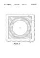
- the present inventionaddresses the thermal stress and mechanical stress induced cracks according to the prior art, by incorporating a stress isolation trench in the passivation layer. More particularly, turning to FIG. 2, a solder bump structure on a semiconductor die 10 is illustrated. As noted above with respect to the prior art, although a single bump structure is illustrated, such bump structures are generally formed in an array pattern across a major surface of the semiconductor die 10, or at least around the periphery of the semiconductor die.
- the bump structureincludes an aluminum pad 12. Aluminum pad 12 is generally formed on the semiconductor die, while it is still in wafer form.
- an aluminum layeris blanket deposited over the entire wafer, photoresist is then deposited on the wafer, the photoresist is patterned and unwanted portions of the aluminum layer are etched away, leaving behind a plurality of bond pads.
- a passivation layer 14is blanket deposited over the entire wafer. Then, a photoresist is deposited so as to overlie the passivation layer, the photoresist is patterned, and unwanted portions of the passivation layer are removed.
- the passivation layeris on the order of 0.5 to 2.0 microns, nominally 1.1 microns.
- the passivation layergenerally has a glassy structure, such as glassy silicon dioxide.
- the passivation layermay also be formed of silicon oxynitride and silicon nitride, for example. Like the prior art, a portion of the passivation layer 14 overlying bond pad 12 is removed, so as to expose bond pad 12. However, according to a particular development of the present invention, a stress isolation trench 15 is formed in the passivation layer, overlying the bond pad 12. Removal of portions of the passivation layer 14 to define the stress isolation trench 15 and the opening to the bond pad 12 may be executed at the same time, by appropriately patterning a photoresist layer overlying the passivation layer 14.
- the stress isolation trenchhas a width generally on the order of 0.5 to 5 microns.
- the trench 15extends completely through the thickness of the passivation layer 14, and overlies the bond pad 12, so as not extend over the edge of the bond pad 12 onto silicon die 10.
- the trenchis generally spaced from the edge of the bond pad 12 by a minimum distance of 3 microns, such as 6 microns, and preferably 10 microns.
- an additional layeris blanket deposited and etched back.
- the polyimide layeradvantageously fills in the stress isolation trench 15.
- under bump metallization (UBM) layer 18is blanket deposited and etched back.
- the UBM layer 18generally includes titanium, tungsten and copper.
- the under bump metallizationis shown as a single layer, it may be formed of multiple layers. Thereafter, the under bump metallization layer 18 is exposed to a bath containing copper, and a copper stud is grown on under bump metallization 18.
- the copper stud 20generally has a thickness on the order of 12 to 45 microns.
- solder bump 22is electroplated so as to overlie the copper stud 20.
- the bumpis generally comprised of lead and tin, preferably, eutectic solder (63% Sn, 37% Pb).
- the structureis reflowed at a temperature on the order of 185 to 220 degrees C., such that solder bump 22 assumes the generally spherical shape shown in FIG. 2.
- the semiconductor die 10is now ready to be bonded to an epoxy printed circuit board according to the DCA process, or to an intermediate substrate, which may be ceramic or plastic.
- the semiconductor die 10is flipped over, and the solder bumps 22 are aligned with conjugate bonding pads on the substrate or circuit board and reflow is carried out to effect mechanical and electrical connection.
- bonding to the circuit board or to a substrateis completed by incorporating an underfill material between the semiconductor die 10 and the respective circuit board or substrate.
- solder bump structurehas been described above with respect to formation of a solder bump by electroplating, it should be well understood that the solder bump may be formed by other techniques, including electroless plating, C4 and E3 processing.
- the process flow for forming the solder bump structureuses conventional techniques, with the exception of patterning the photoresist for defining the stress isolation trench 15. That is, the photoresist is patterned so as to define not only the opening to the bond pad 12 in the passivation layer 14, but also the stress isolation trench 15.
- the polyimide layer 16may be omitted. That is, in processes in which the bond pad is not exposed through the isolation trench during deposition of components of the solder bump, the polyimide layer need not be present to isolate the exposed portion of the bond pad in the trench.
Landscapes
- Engineering & Computer Science (AREA)
- Computer Hardware Design (AREA)
- Microelectronics & Electronic Packaging (AREA)
- Power Engineering (AREA)
- Internal Circuitry In Semiconductor Integrated Circuit Devices (AREA)
Abstract
Description
Claims (13)
Priority Applications (1)
| Application Number | Priority Date | Filing Date | Title |
|---|---|---|---|
| US09/094,974US5943597A (en) | 1998-06-15 | 1998-06-15 | Bumped semiconductor device having a trench for stress relief |
Applications Claiming Priority (1)
| Application Number | Priority Date | Filing Date | Title |
|---|---|---|---|
| US09/094,974US5943597A (en) | 1998-06-15 | 1998-06-15 | Bumped semiconductor device having a trench for stress relief |
Publications (1)
| Publication Number | Publication Date |
|---|---|
| US5943597Atrue US5943597A (en) | 1999-08-24 |
Family
ID=22248281
Family Applications (1)
| Application Number | Title | Priority Date | Filing Date |
|---|---|---|---|
| US09/094,974Expired - Fee RelatedUS5943597A (en) | 1998-06-15 | 1998-06-15 | Bumped semiconductor device having a trench for stress relief |
Country Status (1)
| Country | Link |
|---|---|
| US (1) | US5943597A (en) |
Cited By (101)
| Publication number | Priority date | Publication date | Assignee | Title |
|---|---|---|---|---|
| US6045030A (en)* | 1997-03-13 | 2000-04-04 | Raytheon Company | Sealing electronic packages containing bumped hybrids |
| US6157079A (en)* | 1997-11-10 | 2000-12-05 | Citizen Watch Co., Ltd | Semiconductor device with a bump including a bump electrode film covering a projecting photoresist |
| US6312830B1 (en)* | 1999-09-02 | 2001-11-06 | Intel Corporation | Method and an apparatus for forming an under bump metallization structure |
| US6344695B1 (en)* | 1998-10-12 | 2002-02-05 | Shinko Electric Industries Co., Ltd. | Semiconductor device to be mounted on main circuit board and process for manufacturing same device |
| US6400018B2 (en)* | 1998-08-27 | 2002-06-04 | 3M Innovative Properties Company | Via plug adapter |
| US6424036B1 (en)* | 1998-09-17 | 2002-07-23 | Nec Corporation | Semiconductor device and method for manufacturing the same |
| US6426281B1 (en)* | 2001-01-16 | 2002-07-30 | Taiwan Semiconductor Manufacturing Company | Method to form bump in bumping technology |
| US6429531B1 (en)* | 2000-04-18 | 2002-08-06 | Motorola, Inc. | Method and apparatus for manufacturing an interconnect structure |
| US20020139969A1 (en)* | 2001-03-30 | 2002-10-03 | Fujitsu Quantum Devices Limited | High frequency semiconductor device |
| US6462414B1 (en)* | 1999-03-05 | 2002-10-08 | Altera Corporation | Integrated circuit package utilizing a conductive structure for interlocking a conductive ball to a ball pad |
| US6518665B1 (en)* | 1997-07-11 | 2003-02-11 | Delaware Capital Formation, Inc. | Enhanced underfill adhesion |
| US6538323B1 (en)* | 1998-11-30 | 2003-03-25 | Kabushiki Kaisha Toshiba | Semiconductor device having an electrode structure comprising a conductive fine particle film |
| US6593220B1 (en)* | 2002-01-03 | 2003-07-15 | Taiwan Semiconductor Manufacturing Company | Elastomer plating mask sealed wafer level package method |
| US20030141593A1 (en)* | 2002-01-25 | 2003-07-31 | Zuniga-Ortiz Edgar R. | Flip-chip without bumps and polymer for board assembly |
| US6653563B2 (en)* | 2001-03-30 | 2003-11-25 | Intel Corporation | Alternate bump metallurgy bars for power and ground routing |
| US6692990B2 (en)* | 2000-11-30 | 2004-02-17 | Kabushiki Kaisha Shinkawa | Method for manufacturing a semiconductor device |
| US20040124006A1 (en)* | 2002-12-31 | 2004-07-01 | Pearson Tom E. | Built up lands |
| US6768210B2 (en)* | 2001-11-01 | 2004-07-27 | Texas Instruments Incorporated | Bumpless wafer scale device and board assembly |
| US20040157450A1 (en)* | 2001-12-21 | 2004-08-12 | Bojkov Christo P. | Waferlevel method for direct bumping on copper pads in integrated circuits |
| US6806570B1 (en) | 2002-10-24 | 2004-10-19 | Megic Corporation | Thermal compliant semiconductor chip wiring structure for chip scale packaging |
| US20050032349A1 (en)* | 2001-03-05 | 2005-02-10 | Megic Corporation | Low fabrication cost, fine pitch and high reliability solder bump |
| US20050042872A1 (en)* | 2003-08-21 | 2005-02-24 | Siliconware Precision Industries Co., Ltd., Taiwan, R.O.C. | Process for forming lead-free bump on electronic component |
| US6878642B1 (en)* | 2000-10-06 | 2005-04-12 | Taiwan Semiconductor Manufacturing Company | Method to improve passivation openings by reflow of photoresist to eliminate tape residue |
| WO2005045931A2 (en) | 2003-11-06 | 2005-05-19 | Infineon Technologies Ag | Semiconductor chip having flip-chip contacts and method for producing the same |
| US20050167826A1 (en)* | 2004-02-02 | 2005-08-04 | Zuniga-Ortiz Edgar R. | Bumpless wafer scale device and board assembly |
| US20050200011A1 (en)* | 2004-03-11 | 2005-09-15 | International Rectifier Corporation | Solderable top metalization and passivation for source mounted package |
| US20050260794A1 (en)* | 2002-09-03 | 2005-11-24 | Industrial Technology Research Institute | Method for fabrication of wafer level package incorporating dual compliant layers |
| US20050272257A1 (en)* | 2004-06-03 | 2005-12-08 | International Rectifier Corporation | Semiconductor device with reduced contact resistance |
| US20060068595A1 (en)* | 2004-09-30 | 2006-03-30 | Frank Seliger | Semiconductor substrate thinning method for manufacturing thinned die |
| US20060125094A1 (en)* | 2004-09-20 | 2006-06-15 | Mou-Shiung Lin | Solder interconnect on IC chip |
| US20060148233A1 (en)* | 2001-09-21 | 2006-07-06 | Madhav Datta | Copper-containing C4 ball-limiting metallurgy stack for enhanced reliability of packaged structures and method of making same |
| US20060192298A1 (en)* | 2005-02-07 | 2006-08-31 | Michael Bauer | Semiconductor device with surface-mountable outer contacts, and process for producing it |
| US20060220246A1 (en)* | 2004-12-07 | 2006-10-05 | Kil-Soo Kim | Bump land structure of circuit substrate for semiconductor package |
| US20060246706A1 (en)* | 2005-04-12 | 2006-11-02 | Siliconware Precision Industries Co., Ltd. | Conductive bump structure for semiconductor device and fabrication method thereof |
| EP1665363A4 (en)* | 2003-09-26 | 2006-11-15 | Flip Chip Technologies L L C | Wafer-level moat structures |
| US20070045841A1 (en)* | 2005-08-24 | 2007-03-01 | Cho Won G | Semiconductor chip, display panel using the same, and methods of manufacturing semiconductor chip and display panel using the same |
| US20070090525A1 (en)* | 2005-10-06 | 2007-04-26 | Locker Howard J | System and method for decreasing stress on solder holding BGA module to computer motherboard |
| US20070232053A1 (en)* | 2002-10-24 | 2007-10-04 | Megica Corporation | Method for fabricating thermal compliant semiconductor chip wiring structure for chip scale packaging |
| US20080036086A1 (en)* | 2006-08-11 | 2008-02-14 | Sharp Kabushiki Kaisha | Semiconductor device and method for manufacturing the same |
| US20080048328A1 (en)* | 2001-12-13 | 2008-02-28 | Megica Corporation | Chip structure and process for forming the same |
| US20080050912A1 (en)* | 1998-12-21 | 2008-02-28 | Megica Corporation | Chip structure and process for forming the same |
| US20080067677A1 (en)* | 2001-03-05 | 2008-03-20 | Megica Corporation | Structure and manufacturing method of a chip scale package |
| US20080099928A1 (en)* | 2001-09-17 | 2008-05-01 | Megica Corporation | Low fabrication cost, high performance, high reliability chip scale package |
| US20080148563A1 (en)* | 2000-09-25 | 2008-06-26 | Ibiden Co., Ltd. | Semiconductor element, method of manufacturing semiconductor element, multi-layer printed circuit board, and method of manufacturing multi-layer printed circuit board |
| US20080150134A1 (en)* | 2006-12-25 | 2008-06-26 | Rohm Co., Ltd. | Semiconductor device |
| US20080151520A1 (en)* | 2000-02-25 | 2008-06-26 | Ibiden Co., Ltd. | Multilayer printed circuit board and multilayer printed circuit board manufacturing method |
| US20080224326A1 (en)* | 2003-12-08 | 2008-09-18 | Megica Corporation | Chip structure with bumps and testing pads |
| US20080233733A1 (en)* | 1998-12-21 | 2008-09-25 | Megica Corporation | Method of wire bonding over active area of a semiconductor circuit |
| US7446399B1 (en) | 2004-08-04 | 2008-11-04 | Altera Corporation | Pad structures to improve board-level reliability of solder-on-pad BGA structures |
| US20080284016A1 (en)* | 2001-02-15 | 2008-11-20 | Megica Corporation | Reliable metal bumps on top of I/O pads after removal of test probe marks |
| US20090057892A1 (en)* | 2007-09-04 | 2009-03-05 | Takatoshi Osumi | Electrode structure in semiconductor device and related technology |
| US20090110881A1 (en)* | 2007-10-26 | 2009-04-30 | Daubenspeck Timothy H | Substrate anchor structure and method |
| WO2009108230A1 (en)* | 2007-12-13 | 2009-09-03 | The Timken Company | Sensor module with stress isolated temperature compensation and method of manufacture |
| CN100578809C (en)* | 2004-10-21 | 2010-01-06 | 硅尼克斯科技公司 | Solderable top metal for SiC devices |
| US20100044863A1 (en)* | 2006-12-25 | 2010-02-25 | Rohm Co., Ltd. | Semiconductor device |
| CN101019226B (en)* | 2004-05-28 | 2010-04-07 | 国际整流器公司 | Preparation of front contact for surface mounting |
| CN1871555B (en)* | 2003-09-26 | 2010-08-11 | 倒装晶片技术有限公司 | Forming partial-depth features in polymer film |
| US20100207271A1 (en)* | 2009-02-19 | 2010-08-19 | Toshihiko Omi | Semiconductor device |
| US20100304565A1 (en)* | 2005-06-14 | 2010-12-02 | John Trezza | Processed wafer via |
| US20110027944A1 (en)* | 2009-07-30 | 2011-02-03 | Taiwan Semiconductor Maufacturing Company, Ltd. | Method of forming electrical connections |
| US20110084381A1 (en)* | 2009-10-14 | 2011-04-14 | Jian-Wen Lo | Chip Having A Metal Pillar Structure |
| US20110084389A1 (en)* | 2009-10-14 | 2011-04-14 | Jian-Wen Lo | Semiconductor Device |
| US7960270B2 (en) | 2002-01-07 | 2011-06-14 | Megica Corporation | Method for fabricating circuit component |
| US20110147932A1 (en)* | 2005-06-14 | 2011-06-23 | John Trezza | Contact-based encapsulation |
| US20110193224A1 (en)* | 2010-02-10 | 2011-08-11 | Denso Corporation | Semiconductor device |
| US8021921B2 (en) | 2002-10-25 | 2011-09-20 | Megica Corporation | Method of joining chips utilizing copper pillar |
| US8168527B2 (en) | 2006-09-06 | 2012-05-01 | Megica Corporation | Semiconductor chip and method for fabricating the same |
| US8283781B2 (en) | 2010-09-10 | 2012-10-09 | Taiwan Semiconductor Manufacturing Company, Ltd. | Semiconductor device having pad structure with stress buffer layer |
| US8294279B2 (en) | 2005-01-25 | 2012-10-23 | Megica Corporation | Chip package with dam bar restricting flow of underfill |
| US20130075911A1 (en)* | 2010-04-09 | 2013-03-28 | Renesas Electronics Corporation | Semiconductor Device Having Electrode/Film Opening Edge Spacing Smaller Than Bonding Pad/Electrode Edge Spacing |
| US8481418B2 (en) | 2002-05-01 | 2013-07-09 | Megica Corporation | Low fabrication cost, high performance, high reliability chip scale package |
| US8569162B2 (en)* | 2012-03-22 | 2013-10-29 | Siliconware Precision Industries Co., Ltd. | Conductive bump structure on substrate and fabrication method thereof |
| US8569885B2 (en) | 2010-10-29 | 2013-10-29 | Advanced Semiconductor Engineering, Inc. | Stacked semiconductor packages and related methods |
| US8642384B2 (en)* | 2012-03-09 | 2014-02-04 | Stats Chippac, Ltd. | Semiconductor device and method of forming non-linear interconnect layer with extended length for joint reliability |
| US8686568B2 (en) | 2012-09-27 | 2014-04-01 | Advanced Semiconductor Engineering, Inc. | Semiconductor package substrates having layered circuit segments, and related methods |
| US8698307B2 (en) | 2010-09-27 | 2014-04-15 | Advanced Semiconductor Engineering, Inc. | Semiconductor package with integrated metal pillars and manufacturing methods thereof |
| US8709932B2 (en) | 2010-12-13 | 2014-04-29 | Stats Chippac Ltd. | Integrated circuit packaging system with interconnects and method of manufacture thereof |
| TWI449144B (en)* | 2012-02-16 | 2014-08-11 | 矽品精密工業股份有限公司 | Semiconductor package and its substrate |
| US8884443B2 (en) | 2012-07-05 | 2014-11-11 | Advanced Semiconductor Engineering, Inc. | Substrate for semiconductor package and process for manufacturing |
| US20150132941A1 (en)* | 2009-10-29 | 2015-05-14 | Taiwan Semiconductor Manufacturing Company, Ltd. | Semiconductor Die Contact Structure and Method |
| US9269607B2 (en) | 2014-06-17 | 2016-02-23 | Globalfoundries Inc. | Wafer stress control with backside patterning |
| US20160105959A1 (en)* | 2014-10-13 | 2016-04-14 | Samsung Display Co., Ltd. | Pad electrode structure, flat display apparatus comprising the pad electrode structure, and the method of manufacturing the flat display apparatus |
| US20160163612A1 (en)* | 2014-12-05 | 2016-06-09 | Advanced Semiconductor Engineering, Inc. | Semiconductor package and method of manufacturing the same |
| US9472521B2 (en) | 2012-05-30 | 2016-10-18 | Taiwan Semiconductor Manufacturing Company, Ltd. | Scheme for connector site spacing and resulting structures |
| US9484317B2 (en) | 2012-05-30 | 2016-11-01 | Taiwan Semiconductor Manufacturing Company, Ltd. | Scheme for connector site spacing and resulting structures |
| US9543490B2 (en) | 2010-09-24 | 2017-01-10 | Seoul Semiconductor Co., Ltd. | Wafer-level light emitting diode package and method of fabricating the same |
| CN106328627A (en)* | 2015-06-30 | 2017-01-11 | 台湾积体电路制造股份有限公司 | Stacked semiconductor devices and methods of forming same |
| TWI582928B (en)* | 2016-01-19 | 2017-05-11 | 矽品精密工業股份有限公司 | Substrate structure and method of manufacturing the same |
| EP2605273A3 (en)* | 2011-12-16 | 2017-08-09 | Imec | Method for forming isolation trenches in micro-bump interconnect structures and devices obtained thereof |
| CN108269770A (en)* | 2016-12-30 | 2018-07-10 | 德克萨斯仪器股份有限公司 | With the semiconductor devices of the cylinder of stress relief for discontinuously locating on surface |
| CN108962764A (en)* | 2017-05-22 | 2018-12-07 | 中芯国际集成电路制造(上海)有限公司 | Forming method, semiconductor chip, packaging method and the structure of semiconductor structure |
| US20200051910A1 (en)* | 2017-04-25 | 2020-02-13 | Mitsubishi Electric Corporation | Semiconductor device |
| US10580929B2 (en) | 2016-03-30 | 2020-03-03 | Seoul Viosys Co., Ltd. | UV light emitting diode package and light emitting diode module having the same |
| US11217548B2 (en)* | 2014-03-13 | 2022-01-04 | Taiwan Semiconductor Manufacturing Co., Ltd. | Semiconductor device structure and manufacturing method |
| CN114424334A (en)* | 2020-05-29 | 2022-04-29 | 深圳市汇顶科技股份有限公司 | A chip packaging structure, method and chip module |
| US11342283B2 (en) | 2019-08-12 | 2022-05-24 | Samsung Electronics Co., Ltd. | Package substrate and semiconductor package including the same |
| CN115548110A (en)* | 2022-11-28 | 2022-12-30 | 深圳市威兆半导体股份有限公司 | Semiconductor device and manufacturing method thereof |
| US11600590B2 (en)* | 2019-03-22 | 2023-03-07 | Advanced Semiconductor Engineering, Inc. | Semiconductor device and semiconductor package |
| US20230326893A1 (en)* | 2022-04-07 | 2023-10-12 | Samsung Electronics Co., Ltd. | Semiconductor device and method of fabricating the same |
| US11791286B2 (en) | 2016-09-12 | 2023-10-17 | Samsung Electronics Co., Ltd. | Semiconductor device and semiconductor package |
| CN116913868A (en)* | 2023-09-11 | 2023-10-20 | 深圳市威兆半导体股份有限公司 | Semiconductor device and manufacturing method thereof |
Citations (6)
| Publication number | Priority date | Publication date | Assignee | Title |
|---|---|---|---|---|
| US4048438A (en)* | 1974-10-23 | 1977-09-13 | Amp Incorporated | Conductor patterned substrate providing stress release during direct attachment of integrated circuit chips |
| US5821608A (en)* | 1995-09-08 | 1998-10-13 | Tessera, Inc. | Laterally situated stress/strain relieving lead for a semiconductor chip package |
| US5834848A (en)* | 1996-12-03 | 1998-11-10 | Kabushiki Kaisha Toshiba | Electronic device and semiconductor package |
| US5834374A (en)* | 1994-09-30 | 1998-11-10 | International Business Machines Corporation | Method for controlling tensile and compressive stresses and mechanical problems in thin films on substrates |
| US5844782A (en)* | 1994-12-20 | 1998-12-01 | Sony Corporation | Printed wiring board and electronic device using same |
| US5847456A (en)* | 1996-02-28 | 1998-12-08 | Nec Corporation | Semiconductor device |
- 1998
- 1998-06-15USUS09/094,974patent/US5943597A/ennot_activeExpired - Fee Related
Patent Citations (6)
| Publication number | Priority date | Publication date | Assignee | Title |
|---|---|---|---|---|
| US4048438A (en)* | 1974-10-23 | 1977-09-13 | Amp Incorporated | Conductor patterned substrate providing stress release during direct attachment of integrated circuit chips |
| US5834374A (en)* | 1994-09-30 | 1998-11-10 | International Business Machines Corporation | Method for controlling tensile and compressive stresses and mechanical problems in thin films on substrates |
| US5844782A (en)* | 1994-12-20 | 1998-12-01 | Sony Corporation | Printed wiring board and electronic device using same |
| US5821608A (en)* | 1995-09-08 | 1998-10-13 | Tessera, Inc. | Laterally situated stress/strain relieving lead for a semiconductor chip package |
| US5847456A (en)* | 1996-02-28 | 1998-12-08 | Nec Corporation | Semiconductor device |
| US5834848A (en)* | 1996-12-03 | 1998-11-10 | Kabushiki Kaisha Toshiba | Electronic device and semiconductor package |
Cited By (258)
| Publication number | Priority date | Publication date | Assignee | Title |
|---|---|---|---|---|
| US6045030A (en)* | 1997-03-13 | 2000-04-04 | Raytheon Company | Sealing electronic packages containing bumped hybrids |
| US6518665B1 (en)* | 1997-07-11 | 2003-02-11 | Delaware Capital Formation, Inc. | Enhanced underfill adhesion |
| US6157079A (en)* | 1997-11-10 | 2000-12-05 | Citizen Watch Co., Ltd | Semiconductor device with a bump including a bump electrode film covering a projecting photoresist |
| US6400018B2 (en)* | 1998-08-27 | 2002-06-04 | 3M Innovative Properties Company | Via plug adapter |
| US6424036B1 (en)* | 1998-09-17 | 2002-07-23 | Nec Corporation | Semiconductor device and method for manufacturing the same |
| US6344695B1 (en)* | 1998-10-12 | 2002-02-05 | Shinko Electric Industries Co., Ltd. | Semiconductor device to be mounted on main circuit board and process for manufacturing same device |
| US6933216B2 (en) | 1998-11-30 | 2005-08-23 | Kabushiki Kaisha Toshiba | Fine particle film forming apparatus and method and semiconductor device and manufacturing method for the same |
| US20050124164A1 (en)* | 1998-11-30 | 2005-06-09 | Kabushiki Kaisha Toshiba | Fine particle film forming apparatus and method and semiconductor device and manufacturing method for the same |
| US20030122252A1 (en)* | 1998-11-30 | 2003-07-03 | Kabushiki Kaisha Toshiba | Fine particle film forming apparatus and method and semiconductor device and manufacturing method for the same |
| US6538323B1 (en)* | 1998-11-30 | 2003-03-25 | Kabushiki Kaisha Toshiba | Semiconductor device having an electrode structure comprising a conductive fine particle film |
| US8138079B2 (en) | 1998-12-21 | 2012-03-20 | Megica Corporation | Method of wire bonding over active area of a semiconductor circuit |
| US20080136034A1 (en)* | 1998-12-21 | 2008-06-12 | Megica Corporation | Chip structure and process for forming the same |
| US20080124918A1 (en)* | 1998-12-21 | 2008-05-29 | Megica Corporation | Chip structure and process for forming the same |
| US7906849B2 (en) | 1998-12-21 | 2011-03-15 | Megica Corporation | Chip structure and process for forming the same |
| US7906422B2 (en) | 1998-12-21 | 2011-03-15 | Megica Corporation | Chip structure and process for forming the same |
| US20080233733A1 (en)* | 1998-12-21 | 2008-09-25 | Megica Corporation | Method of wire bonding over active area of a semiconductor circuit |
| US20080050912A1 (en)* | 1998-12-21 | 2008-02-28 | Megica Corporation | Chip structure and process for forming the same |
| US7915157B2 (en) | 1998-12-21 | 2011-03-29 | Megica Corporation | Chip structure and process for forming the same |
| US20020194731A1 (en)* | 1999-03-05 | 2002-12-26 | Altera Corporation | Fabrication method and structure of an integrated circuit package |
| US6462414B1 (en)* | 1999-03-05 | 2002-10-08 | Altera Corporation | Integrated circuit package utilizing a conductive structure for interlocking a conductive ball to a ball pad |
| US6929978B2 (en) | 1999-03-05 | 2005-08-16 | Altera Corporation | Method of fabricating an integrated circuit package utilizing a conductive structure for improving the bond strength between an IC package and a printed circuit board |
| US6461954B1 (en) | 1999-09-02 | 2002-10-08 | Intel Corporation | Method and an apparatus for forming an under bump metallization structure |
| US6312830B1 (en)* | 1999-09-02 | 2001-11-06 | Intel Corporation | Method and an apparatus for forming an under bump metallization structure |
| US20080201944A1 (en)* | 2000-02-25 | 2008-08-28 | Ibiden Co., Ltd. | Multilayer printed circuit board and multilayer printed circuit board manufacturing method |
| US8079142B2 (en) | 2000-02-25 | 2011-12-20 | Ibiden Co., Ltd. | Printed circuit board manufacturing method |
| US7884286B2 (en) | 2000-02-25 | 2011-02-08 | Ibiden Co., Ltd. | Multilayer printed circuit board |
| US8438727B2 (en)* | 2000-02-25 | 2013-05-14 | Ibiden Co., Ltd. | Multilayer printed circuit board and multilayer printed circuit board manufacturing method |
| US8453323B2 (en) | 2000-02-25 | 2013-06-04 | Ibiden Co., Ltd. | Printed circuit board manufacturing method |
| US20080151520A1 (en)* | 2000-02-25 | 2008-06-26 | Ibiden Co., Ltd. | Multilayer printed circuit board and multilayer printed circuit board manufacturing method |
| US20100031503A1 (en)* | 2000-02-25 | 2010-02-11 | Ibiden Co., Ltd. | Multilayer printed circuit board and multilayer printed circuit board manufacturing method |
| US20080151519A1 (en)* | 2000-02-25 | 2008-06-26 | Ibiden Co., Ltd. | Multilayer printed circuit board and multilayer printed circuit board manufacturing method |
| US20090070996A1 (en)* | 2000-02-25 | 2009-03-19 | Ibiden Co., Ltd. | Printed circuit board manufacturing method |
| US8046914B2 (en) | 2000-02-25 | 2011-11-01 | Ibiden Co., Ltd. | Method for manufacturing multilayer printed circuit board |
| US20080151517A1 (en)* | 2000-02-25 | 2008-06-26 | Ibiden Co., Ltd. | Multilayer printed circuit board and multilayer printed circuit board manufacturing method |
| US7888605B2 (en) | 2000-02-25 | 2011-02-15 | Ibiden Co., Ltd. | Multilayer printed circuit board |
| US8186045B2 (en) | 2000-02-25 | 2012-05-29 | Ibiden Co., Ltd. | Multilayer printed circuit board and multilayer printed circuit board manufacturing method |
| US20100018049A1 (en)* | 2000-02-25 | 2010-01-28 | Ibiden Co., Ltd. | Multilayer printed circuit board and multilayer printed circuit board manufacturing method |
| US7888606B2 (en) | 2000-02-25 | 2011-02-15 | Ibiden Co., Ltd. | Multilayer printed circuit board |
| US6429531B1 (en)* | 2000-04-18 | 2002-08-06 | Motorola, Inc. | Method and apparatus for manufacturing an interconnect structure |
| US20090077796A1 (en)* | 2000-09-25 | 2009-03-26 | Ibiden Co., Ltd. | Semiconductor element, method of manufacturing semiconductor element, multi-layer printed circuit board, and method of manufacturing multi-layer printed circuit board |
| US20080151522A1 (en)* | 2000-09-25 | 2008-06-26 | Ibiden Co., Ltd. | Semiconductor element, method of manufacturing semiconductor element, multi-layer printed circuit board, and method of manufacturing multi-layer printed circuit board |
| US7908745B2 (en) | 2000-09-25 | 2011-03-22 | Ibiden Co., Ltd. | Method of manufacturing multi-layer printed circuit board |
| US20080206926A1 (en)* | 2000-09-25 | 2008-08-28 | Ibiden Co., Ltd. | Semiconductor element, method of manufacturing semiconductor element, multi-layer printed circuit board, and method of manufacturing multi-layer printed circuit board |
| US7999387B2 (en)* | 2000-09-25 | 2011-08-16 | Ibiden Co., Ltd. | Semiconductor element connected to printed circuit board |
| US8822323B2 (en) | 2000-09-25 | 2014-09-02 | Ibiden Co., Ltd. | Semiconductor element, method of manufacturing semiconductor element, multi-layer printed circuit board, and method of manufacturing multi-layer printed circuit board |
| US8067699B2 (en) | 2000-09-25 | 2011-11-29 | Ibiden Co., Ltd. | Semiconductor element, method of manufacturing semiconductor element, multi-layer printed circuit board, and method of manufacturing multi-layer printed circuit board |
| US20080230914A1 (en)* | 2000-09-25 | 2008-09-25 | Ibiden Co., Ltd. | Semiconductor element, method of manufacturing semiconductor element, multi-layer printed circuit board, and method of manufacturing multi-layer printed circuit board |
| US8959756B2 (en) | 2000-09-25 | 2015-02-24 | Ibiden Co., Ltd. | Method of manufacturing a printed circuit board having an embedded electronic component |
| US8524535B2 (en) | 2000-09-25 | 2013-09-03 | Ibiden Co., Ltd. | Semiconductor element, method of manufacturing semiconductor element, multi-layer printed circuit board, and method of manufacturing multi-layer printed circuit board |
| US9245838B2 (en) | 2000-09-25 | 2016-01-26 | Ibiden Co., Ltd. | Semiconductor element |
| US8293579B2 (en) | 2000-09-25 | 2012-10-23 | Ibiden Co., Ltd. | Semiconductor element, method of manufacturing semiconductor element, multi-layer printed circuit board, and method of manufacturing multi-layer printed circuit board |
| US20090263939A1 (en)* | 2000-09-25 | 2009-10-22 | Ibiden Co., Ltd. | Semiconductor element, method of manufacturing semiconductor element, multi-layer printed circuit board, and method of manufacturing multi-layer printed circuit board |
| US20080148563A1 (en)* | 2000-09-25 | 2008-06-26 | Ibiden Co., Ltd. | Semiconductor element, method of manufacturing semiconductor element, multi-layer printed circuit board, and method of manufacturing multi-layer printed circuit board |
| US6878642B1 (en)* | 2000-10-06 | 2005-04-12 | Taiwan Semiconductor Manufacturing Company | Method to improve passivation openings by reflow of photoresist to eliminate tape residue |
| US6879027B2 (en)* | 2000-11-30 | 2005-04-12 | Kabushiki Kaisha Shinkawa | Semiconductor device having bumps |
| US6692990B2 (en)* | 2000-11-30 | 2004-02-17 | Kabushiki Kaisha Shinkawa | Method for manufacturing a semiconductor device |
| US6426281B1 (en)* | 2001-01-16 | 2002-07-30 | Taiwan Semiconductor Manufacturing Company | Method to form bump in bumping technology |
| US20080284016A1 (en)* | 2001-02-15 | 2008-11-20 | Megica Corporation | Reliable metal bumps on top of I/O pads after removal of test probe marks |
| US8901733B2 (en) | 2001-02-15 | 2014-12-02 | Qualcomm Incorporated | Reliable metal bumps on top of I/O pads after removal of test probe marks |
| US20080048320A1 (en)* | 2001-03-05 | 2008-02-28 | Megica Corporation | Low fabrication cost, fine pitch and high reliability solder bump |
| US20080067677A1 (en)* | 2001-03-05 | 2008-03-20 | Megica Corporation | Structure and manufacturing method of a chip scale package |
| US20080088019A1 (en)* | 2001-03-05 | 2008-04-17 | Megica Corporation | Structure and manufacturing method of a chip scale package |
| US8072070B2 (en) | 2001-03-05 | 2011-12-06 | Megica Corporation | Low fabrication cost, fine pitch and high reliability solder bump |
| US7902679B2 (en) | 2001-03-05 | 2011-03-08 | Megica Corporation | Structure and manufacturing method of a chip scale package with low fabrication cost, fine pitch and high reliability solder bump |
| US7863739B2 (en) | 2001-03-05 | 2011-01-04 | Megica Corporation | Low fabrication cost, fine pitch and high reliability solder bump |
| US20090261473A1 (en)* | 2001-03-05 | 2009-10-22 | Megica Corporation | Low fabrication cost, fine pitch and high reliability solder bump |
| US20050032349A1 (en)* | 2001-03-05 | 2005-02-10 | Megic Corporation | Low fabrication cost, fine pitch and high reliability solder bump |
| US20090267213A1 (en)* | 2001-03-05 | 2009-10-29 | Megica Corporation | Structure and manufacturing method of a chip scale package with low fabrication cost, fine pitch and high reliability solder bump |
| US8368213B2 (en) | 2001-03-05 | 2013-02-05 | Megica Corporation | Low fabrication cost, fine pitch and high reliability solder bump |
| US8158508B2 (en) | 2001-03-05 | 2012-04-17 | Megica Corporation | Structure and manufacturing method of a chip scale package |
| US6653563B2 (en)* | 2001-03-30 | 2003-11-25 | Intel Corporation | Alternate bump metallurgy bars for power and ground routing |
| US6787909B2 (en) | 2001-03-30 | 2004-09-07 | Fujitsu Quantum Devices Limited | High frequency semiconductor device |
| US20020139969A1 (en)* | 2001-03-30 | 2002-10-03 | Fujitsu Quantum Devices Limited | High frequency semiconductor device |
| US20080099928A1 (en)* | 2001-09-17 | 2008-05-01 | Megica Corporation | Low fabrication cost, high performance, high reliability chip scale package |
| US20100038803A9 (en)* | 2001-09-17 | 2010-02-18 | Megica Corporation | Low fabrication cost, high performance, high reliability chip scale package |
| US8178967B2 (en) | 2001-09-17 | 2012-05-15 | Megica Corporation | Low fabrication cost, high performance, high reliability chip scale package |
| US9369175B2 (en) | 2001-09-17 | 2016-06-14 | Qualcomm Incorporated | Low fabrication cost, high performance, high reliability chip scale package |
| US20060148233A1 (en)* | 2001-09-21 | 2006-07-06 | Madhav Datta | Copper-containing C4 ball-limiting metallurgy stack for enhanced reliability of packaged structures and method of making same |
| US20100117229A1 (en)* | 2001-09-21 | 2010-05-13 | Madhav Datta | Copper-containing C4 ball-limiting metallurgy stack for enhanced reliability of packaged structures and method of making same |
| US10037956B2 (en)* | 2001-09-21 | 2018-07-31 | Intel Corporation | Copper-containing C4 ball-limiting metallurgy stack for enhanced reliability of packaged structures and method of making same |
| US8952550B2 (en) | 2001-09-21 | 2015-02-10 | Intel Corporation | Copper-containing C4 ball-limiting metallurgy stack for enhanced reliability of packaged structures and method of making same |
| US20170141062A1 (en)* | 2001-09-21 | 2017-05-18 | Intel Corporation | Copper-containing c4 ball-limiting metallurgy stack for enhanced reliability of packaged structures and method of making same |
| US20150132940A1 (en)* | 2001-09-21 | 2015-05-14 | Intel Corporation | Copper-containing c4 ball-limiting metallurgy stack for enhanced reliability of packaged structures and method of making same |
| US6768210B2 (en)* | 2001-11-01 | 2004-07-27 | Texas Instruments Incorporated | Bumpless wafer scale device and board assembly |
| US20080142979A1 (en)* | 2001-12-13 | 2008-06-19 | Megica Corporation | Chip structure and process for forming the same |
| US7932603B2 (en) | 2001-12-13 | 2011-04-26 | Megica Corporation | Chip structure and process for forming the same |
| US7919867B2 (en) | 2001-12-13 | 2011-04-05 | Megica Corporation | Chip structure and process for forming the same |
| US7915734B2 (en) | 2001-12-13 | 2011-03-29 | Megica Corporation | Chip structure and process for forming the same |
| US8546947B2 (en) | 2001-12-13 | 2013-10-01 | Megica Corporation | Chip structure and process for forming the same |
| US8008776B2 (en) | 2001-12-13 | 2011-08-30 | Megica Corporation | Chip structure and process for forming the same |
| US20080142978A1 (en)* | 2001-12-13 | 2008-06-19 | Megica Corporation | Chip structure and process for forming the same |
| US20080048328A1 (en)* | 2001-12-13 | 2008-02-28 | Megica Corporation | Chip structure and process for forming the same |
| US20080122099A1 (en)* | 2001-12-13 | 2008-05-29 | Megica Corporation | Chip structure and process for forming the same |
| US20040157450A1 (en)* | 2001-12-21 | 2004-08-12 | Bojkov Christo P. | Waferlevel method for direct bumping on copper pads in integrated circuits |
| US6593220B1 (en)* | 2002-01-03 | 2003-07-15 | Taiwan Semiconductor Manufacturing Company | Elastomer plating mask sealed wafer level package method |
| US8461679B2 (en)* | 2002-01-07 | 2013-06-11 | Megica Corporation | Method for fabricating circuit component |
| US7960270B2 (en) | 2002-01-07 | 2011-06-14 | Megica Corporation | Method for fabricating circuit component |
| US20110215476A1 (en)* | 2002-01-07 | 2011-09-08 | Megica Corporation | Method for fabricating circuit component |
| US8890336B2 (en) | 2002-01-07 | 2014-11-18 | Qualcomm Incorporated | Cylindrical bonding structure and method of manufacture |
| US20030141593A1 (en)* | 2002-01-25 | 2003-07-31 | Zuniga-Ortiz Edgar R. | Flip-chip without bumps and polymer for board assembly |
| US6914332B2 (en)* | 2002-01-25 | 2005-07-05 | Texas Instruments Incorporated | Flip-chip without bumps and polymer for board assembly |
| US20060006532A1 (en)* | 2002-01-25 | 2006-01-12 | Zuniga-Ortiz Edgar R | Flip-chip without bumps and polymer for board assembly |
| EP1333494A3 (en)* | 2002-01-25 | 2006-06-07 | Texas Instruments Incorporated | Semiconductor device and method of fabricating a semiconductor assembly |
| US8481418B2 (en) | 2002-05-01 | 2013-07-09 | Megica Corporation | Low fabrication cost, high performance, high reliability chip scale package |
| US7329563B2 (en)* | 2002-09-03 | 2008-02-12 | Industrial Technology Research Institute | Method for fabrication of wafer level package incorporating dual compliant layers |
| US20050260794A1 (en)* | 2002-09-03 | 2005-11-24 | Industrial Technology Research Institute | Method for fabrication of wafer level package incorporating dual compliant layers |
| US8026588B2 (en) | 2002-10-15 | 2011-09-27 | Megica Corporation | Method of wire bonding over active area of a semiconductor circuit |
| US9142527B2 (en) | 2002-10-15 | 2015-09-22 | Qualcomm Incorporated | Method of wire bonding over active area of a semiconductor circuit |
| US8742580B2 (en) | 2002-10-15 | 2014-06-03 | Megit Acquisition Corp. | Method of wire bonding over active area of a semiconductor circuit |
| US9153555B2 (en) | 2002-10-15 | 2015-10-06 | Qualcomm Incorporated | Method of wire bonding over active area of a semiconductor circuit |
| US8021976B2 (en) | 2002-10-15 | 2011-09-20 | Megica Corporation | Method of wire bonding over active area of a semiconductor circuit |
| US7960272B2 (en) | 2002-10-24 | 2011-06-14 | Megica Corporation | Method for fabricating thermal compliant semiconductor chip wiring structure for chip scale packaging |
| US20070232053A1 (en)* | 2002-10-24 | 2007-10-04 | Megica Corporation | Method for fabricating thermal compliant semiconductor chip wiring structure for chip scale packaging |
| US6806570B1 (en) | 2002-10-24 | 2004-10-19 | Megic Corporation | Thermal compliant semiconductor chip wiring structure for chip scale packaging |
| US8334588B2 (en) | 2002-10-24 | 2012-12-18 | Megica Corporation | Circuit component with conductive layer structure |
| US8021921B2 (en) | 2002-10-25 | 2011-09-20 | Megica Corporation | Method of joining chips utilizing copper pillar |
| US8421222B2 (en) | 2002-10-25 | 2013-04-16 | Megica Corporation | Chip package having a chip combined with a substrate via a copper pillar |
| US20040124006A1 (en)* | 2002-12-31 | 2004-07-01 | Pearson Tom E. | Built up lands |
| US20050042872A1 (en)* | 2003-08-21 | 2005-02-24 | Siliconware Precision Industries Co., Ltd., Taiwan, R.O.C. | Process for forming lead-free bump on electronic component |
| US7341949B2 (en)* | 2003-08-21 | 2008-03-11 | Siliconware Precision Industries Co., Ltd. | Process for forming lead-free bump on electronic component |
| CN1871555B (en)* | 2003-09-26 | 2010-08-11 | 倒装晶片技术有限公司 | Forming partial-depth features in polymer film |
| EP1665363A4 (en)* | 2003-09-26 | 2006-11-15 | Flip Chip Technologies L L C | Wafer-level moat structures |
| US7768137B2 (en) | 2003-11-06 | 2010-08-03 | Infineon Technologies Ag | Semiconductor chip with flip chip contacts and a passivation layer with varying thickness portions surrounding contact surfaces of the semiconductor chip |
| WO2005045931A3 (en)* | 2003-11-06 | 2005-08-11 | Infineon Technologies Ag | Semiconductor chip having flip-chip contacts and method for producing the same |
| US20060270163A1 (en)* | 2003-11-06 | 2006-11-30 | Gerald Ofner | Semiconductor chip with flip chip contacts, and method for producing semiconductor chip with flip chip contacts |
| DE10352349B4 (en)* | 2003-11-06 | 2006-11-16 | Infineon Technologies Ag | Semiconductor chip with flip-chip contacts and method for producing the same |
| WO2005045931A2 (en) | 2003-11-06 | 2005-05-19 | Infineon Technologies Ag | Semiconductor chip having flip-chip contacts and method for producing the same |
| DE10352349A1 (en)* | 2003-11-06 | 2005-06-23 | Infineon Technologies Ag | Semiconductor chip with flip-chip contacts and method for producing the same |
| US20080224326A1 (en)* | 2003-12-08 | 2008-09-18 | Megica Corporation | Chip structure with bumps and testing pads |
| US7855461B2 (en) | 2003-12-08 | 2010-12-21 | Megica Corporation | Chip structure with bumps and testing pads |
| US20050167826A1 (en)* | 2004-02-02 | 2005-08-04 | Zuniga-Ortiz Edgar R. | Bumpless wafer scale device and board assembly |
| US7910471B2 (en) | 2004-02-02 | 2011-03-22 | Texas Instruments Incorporated | Bumpless wafer scale device and board assembly |
| US8368211B2 (en)* | 2004-03-11 | 2013-02-05 | International Rectifier Corporation | Solderable top metalization and passivation for source mounted package |
| US9852939B2 (en) | 2004-03-11 | 2017-12-26 | Infineon Technologies Americas Corp. | Solderable contact and passivation for semiconductor dies |
| US9852940B2 (en) | 2004-03-11 | 2017-12-26 | Infineon Technologies Americas Corp. | Method for forming a reliable solderable contact |
| CN1734755B (en)* | 2004-03-11 | 2012-12-19 | 国际整流器公司 | Solderable top metalization and passivation for source mounted package |
| US20050200011A1 (en)* | 2004-03-11 | 2005-09-15 | International Rectifier Corporation | Solderable top metalization and passivation for source mounted package |
| CN101019226B (en)* | 2004-05-28 | 2010-04-07 | 国际整流器公司 | Preparation of front contact for surface mounting |
| US7678680B2 (en)* | 2004-06-03 | 2010-03-16 | International Rectifier Corporation | Semiconductor device with reduced contact resistance |
| US20050272257A1 (en)* | 2004-06-03 | 2005-12-08 | International Rectifier Corporation | Semiconductor device with reduced contact resistance |
| US7446399B1 (en) | 2004-08-04 | 2008-11-04 | Altera Corporation | Pad structures to improve board-level reliability of solder-on-pad BGA structures |
| US20060125094A1 (en)* | 2004-09-20 | 2006-06-15 | Mou-Shiung Lin | Solder interconnect on IC chip |
| US8067837B2 (en) | 2004-09-20 | 2011-11-29 | Megica Corporation | Metallization structure over passivation layer for IC chip |
| US8742582B2 (en) | 2004-09-20 | 2014-06-03 | Megit Acquisition Corp. | Solder interconnect on IC chip |
| US7375032B2 (en)* | 2004-09-30 | 2008-05-20 | Advanced Micro Devices, Inc. | Semiconductor substrate thinning method for manufacturing thinned die |
| US20060068595A1 (en)* | 2004-09-30 | 2006-03-30 | Frank Seliger | Semiconductor substrate thinning method for manufacturing thinned die |
| CN100578809C (en)* | 2004-10-21 | 2010-01-06 | 硅尼克斯科技公司 | Solderable top metal for SiC devices |
| US20060220246A1 (en)* | 2004-12-07 | 2006-10-05 | Kil-Soo Kim | Bump land structure of circuit substrate for semiconductor package |
| US8294279B2 (en) | 2005-01-25 | 2012-10-23 | Megica Corporation | Chip package with dam bar restricting flow of underfill |
| US7408241B2 (en) | 2005-02-07 | 2008-08-05 | Infineon Technologies Ag | Semiconductor device with a recessed bond pad |
| US20060192298A1 (en)* | 2005-02-07 | 2006-08-31 | Michael Bauer | Semiconductor device with surface-mountable outer contacts, and process for producing it |
| US20060246706A1 (en)* | 2005-04-12 | 2006-11-02 | Siliconware Precision Industries Co., Ltd. | Conductive bump structure for semiconductor device and fabrication method thereof |
| US20100297842A1 (en)* | 2005-04-12 | 2010-11-25 | Siliconware Precision Industries Co., Ltd. | Conductive bump structure for semiconductor device and fabrication method thereof |
| US8846445B2 (en) | 2005-06-14 | 2014-09-30 | Cufer Asset Ltd. L.L.C. | Inverse chip connector |
| US10340239B2 (en) | 2005-06-14 | 2019-07-02 | Cufer Asset Ltd. L.L.C | Tooling for coupling multiple electronic chips |
| US9324629B2 (en) | 2005-06-14 | 2016-04-26 | Cufer Asset Ltd. L.L.C. | Tooling for coupling multiple electronic chips |
| US20110147932A1 (en)* | 2005-06-14 | 2011-06-23 | John Trezza | Contact-based encapsulation |
| US9754907B2 (en) | 2005-06-14 | 2017-09-05 | Cufer Asset Ltd. L.L.C. | Tooling for coupling multiple electronic chips |
| US9147635B2 (en)* | 2005-06-14 | 2015-09-29 | Cufer Asset Ltd. L.L.C. | Contact-based encapsulation |
| US8643186B2 (en) | 2005-06-14 | 2014-02-04 | Cufer Asset Ltd. L.L.C. | Processed wafer via |
| US20100304565A1 (en)* | 2005-06-14 | 2010-12-02 | John Trezza | Processed wafer via |
| TWI419292B (en)* | 2005-08-24 | 2013-12-11 | Samsung Display Co Ltd | Semiconductor chip, display panel using the same, and methods of manufacturing semiconductor chip and display panel using the same |
| US7750469B2 (en)* | 2005-08-24 | 2010-07-06 | Samsung Electronics Co., Ltd. | Insulating layer between bumps of semiconductor chip, and display panel using the same with anisotropic conductive film between semiconductor chip and substrate |
| US20070045841A1 (en)* | 2005-08-24 | 2007-03-01 | Cho Won G | Semiconductor chip, display panel using the same, and methods of manufacturing semiconductor chip and display panel using the same |
| CN1921095B (en)* | 2005-08-24 | 2012-05-09 | 三星电子株式会社 | Semiconductor chip, display panel using the same, and methods of manufacturing semiconductor chip and display panel using the same |
| CN1946263B (en)* | 2005-10-06 | 2014-10-01 | 联想(新加坡)私人有限公司 | System and method for decreasing stress on circuit board and mobile processing device |
| US7492044B2 (en)* | 2005-10-06 | 2009-02-17 | Lenovo (Singapore) Pte. Ltd. | System and method for decreasing stress on solder holding BGA module to computer motherboard |
| US20070090525A1 (en)* | 2005-10-06 | 2007-04-26 | Locker Howard J | System and method for decreasing stress on solder holding BGA module to computer motherboard |
| US20080036086A1 (en)* | 2006-08-11 | 2008-02-14 | Sharp Kabushiki Kaisha | Semiconductor device and method for manufacturing the same |
| US7667336B2 (en)* | 2006-08-11 | 2010-02-23 | Sharp Kabushiki Kaisha | Semiconductor device and method for manufacturing the same |
| US8168527B2 (en) | 2006-09-06 | 2012-05-01 | Megica Corporation | Semiconductor chip and method for fabricating the same |
| US20080150134A1 (en)* | 2006-12-25 | 2008-06-26 | Rohm Co., Ltd. | Semiconductor device |
| US20100044863A1 (en)* | 2006-12-25 | 2010-02-25 | Rohm Co., Ltd. | Semiconductor device |
| US9018762B2 (en) | 2006-12-25 | 2015-04-28 | Rohm Co., Ltd. | Semiconductor device bonding with stress relief connection pads |
| US8643180B2 (en)* | 2006-12-25 | 2014-02-04 | Rohm Co., Ltd. | Semiconductor device |
| EP2099065A4 (en)* | 2006-12-25 | 2011-02-23 | Rohm Co Ltd | Semiconductor device |
| US8446008B2 (en) | 2006-12-25 | 2013-05-21 | Rohm Co., Ltd. | Semiconductor device bonding with stress relief connection pads |
| US20090057892A1 (en)* | 2007-09-04 | 2009-03-05 | Takatoshi Osumi | Electrode structure in semiconductor device and related technology |
| US7825513B2 (en)* | 2007-09-04 | 2010-11-02 | Panasonic Corporation | Electrode structure in semiconductor device and related technology |
| US20090110881A1 (en)* | 2007-10-26 | 2009-04-30 | Daubenspeck Timothy H | Substrate anchor structure and method |
| US8361598B2 (en) | 2007-10-26 | 2013-01-29 | International Business Machines Corporation | Substrate anchor structure and method |
| US7935408B2 (en)* | 2007-10-26 | 2011-05-03 | International Business Machines Corporation | Substrate anchor structure and method |
| US20110100685A1 (en)* | 2007-10-26 | 2011-05-05 | International Business Machines Corporation | Substrate anchor structure and method |
| WO2009108230A1 (en)* | 2007-12-13 | 2009-09-03 | The Timken Company | Sensor module with stress isolated temperature compensation and method of manufacture |
| US20100207271A1 (en)* | 2009-02-19 | 2010-08-19 | Toshihiko Omi | Semiconductor device |
| US8377816B2 (en)* | 2009-07-30 | 2013-02-19 | Taiwan Semiconductor Manufacturing Company, Ltd. | Method of forming electrical connections |
| US20110027944A1 (en)* | 2009-07-30 | 2011-02-03 | Taiwan Semiconductor Maufacturing Company, Ltd. | Method of forming electrical connections |
| US20110084389A1 (en)* | 2009-10-14 | 2011-04-14 | Jian-Wen Lo | Semiconductor Device |
| US20110084381A1 (en)* | 2009-10-14 | 2011-04-14 | Jian-Wen Lo | Chip Having A Metal Pillar Structure |
| US8334594B2 (en) | 2009-10-14 | 2012-12-18 | Advanced Semiconductor Engineering, Inc. | Chip having a metal pillar structure |
| US8552553B2 (en) | 2009-10-14 | 2013-10-08 | Advanced Semiconductor Engineering, Inc. | Semiconductor device |
| US10163785B2 (en) | 2009-10-29 | 2018-12-25 | Taiwan Semiconductor Manufacturing Company, Ltd. | Semiconductor die contact structure and method |
| US10847459B2 (en) | 2009-10-29 | 2020-11-24 | Taiwan Semiconductor Manufacturing Company, Ltd. | Semiconductor die contact structure and method |
| US11515272B2 (en) | 2009-10-29 | 2022-11-29 | Taiwan Semiconductor Manufacturing Company, Ltd. | Semiconductor die contact structure and method |
| US20150132941A1 (en)* | 2009-10-29 | 2015-05-14 | Taiwan Semiconductor Manufacturing Company, Ltd. | Semiconductor Die Contact Structure and Method |
| US12074127B2 (en) | 2009-10-29 | 2024-08-27 | Taiwan Semiconductor Manufacturing Company, Ltd. | Semiconductor die contact structure and method |
| US9536811B2 (en)* | 2009-10-29 | 2017-01-03 | Taiwan Semiconductor Manufacturing Company, Ltd. | Semiconductor die contact structure and method |
| US20110193224A1 (en)* | 2010-02-10 | 2011-08-11 | Denso Corporation | Semiconductor device |
| US20130075911A1 (en)* | 2010-04-09 | 2013-03-28 | Renesas Electronics Corporation | Semiconductor Device Having Electrode/Film Opening Edge Spacing Smaller Than Bonding Pad/Electrode Edge Spacing |
| US8587135B2 (en)* | 2010-04-09 | 2013-11-19 | Renesas Electronics Corporation | Semiconductor device having electrode/film opening edge spacing smaller than bonding pad/electrode edge spacing |
| US8283781B2 (en) | 2010-09-10 | 2012-10-09 | Taiwan Semiconductor Manufacturing Company, Ltd. | Semiconductor device having pad structure with stress buffer layer |
| US10879437B2 (en) | 2010-09-24 | 2020-12-29 | Seoul Semiconductor Co., Ltd. | Wafer-level light emitting diode package and method of fabricating the same |
| US10069048B2 (en) | 2010-09-24 | 2018-09-04 | Seoul Viosys Co., Ltd. | Wafer-level light emitting diode package and method of fabricating the same |
| US10892386B2 (en) | 2010-09-24 | 2021-01-12 | Seoul Semiconductor Co., Ltd. | Wafer-level light emitting diode package and method of fabricating the same |
| US9882102B2 (en) | 2010-09-24 | 2018-01-30 | Seoul Semiconductor Co., Ltd. | Wafer-level light emitting diode and wafer-level light emitting diode package |
| US9543490B2 (en) | 2010-09-24 | 2017-01-10 | Seoul Semiconductor Co., Ltd. | Wafer-level light emitting diode package and method of fabricating the same |
| US8698307B2 (en) | 2010-09-27 | 2014-04-15 | Advanced Semiconductor Engineering, Inc. | Semiconductor package with integrated metal pillars and manufacturing methods thereof |
| US8569885B2 (en) | 2010-10-29 | 2013-10-29 | Advanced Semiconductor Engineering, Inc. | Stacked semiconductor packages and related methods |
| US8709932B2 (en) | 2010-12-13 | 2014-04-29 | Stats Chippac Ltd. | Integrated circuit packaging system with interconnects and method of manufacture thereof |
| EP2605273A3 (en)* | 2011-12-16 | 2017-08-09 | Imec | Method for forming isolation trenches in micro-bump interconnect structures and devices obtained thereof |
| TWI449144B (en)* | 2012-02-16 | 2014-08-11 | 矽品精密工業股份有限公司 | Semiconductor package and its substrate |
| US8642384B2 (en)* | 2012-03-09 | 2014-02-04 | Stats Chippac, Ltd. | Semiconductor device and method of forming non-linear interconnect layer with extended length for joint reliability |
| US9117812B2 (en) | 2012-03-09 | 2015-08-25 | Stats Chippac, Ltd. | Semiconductor device and method of forming non-linear interconnect layer with extended length for joint reliability |
| US8569162B2 (en)* | 2012-03-22 | 2013-10-29 | Siliconware Precision Industries Co., Ltd. | Conductive bump structure on substrate and fabrication method thereof |
| TWI497669B (en)* | 2012-03-22 | 2015-08-21 | 矽品精密工業股份有限公司 | Conductive bump of semiconductor substrate and method of forming same |
| US10504856B2 (en) | 2012-05-30 | 2019-12-10 | Taiwan Semiconductor Manufacturing Company, Ltd. | Scheme for connector site spacing and resulting structures |
| US10985114B2 (en) | 2012-05-30 | 2021-04-20 | Taiwan Semiconductor Manufacturing Company, Ltd. | Scheme for connector site spacing and resulting structures |
| US9484317B2 (en) | 2012-05-30 | 2016-11-01 | Taiwan Semiconductor Manufacturing Company, Ltd. | Scheme for connector site spacing and resulting structures |
| US9472521B2 (en) | 2012-05-30 | 2016-10-18 | Taiwan Semiconductor Manufacturing Company, Ltd. | Scheme for connector site spacing and resulting structures |
| US8884443B2 (en) | 2012-07-05 | 2014-11-11 | Advanced Semiconductor Engineering, Inc. | Substrate for semiconductor package and process for manufacturing |
| US9224707B2 (en) | 2012-07-05 | 2015-12-29 | Advanced Semiconductor Engineering, Inc. | Substrate for semiconductor package and process for manufacturing |
| US9437532B2 (en) | 2012-07-05 | 2016-09-06 | Advanced Semiconductor Engineering, Inc. | Substrate for semiconductor package and process for manufacturing |
| US8686568B2 (en) | 2012-09-27 | 2014-04-01 | Advanced Semiconductor Engineering, Inc. | Semiconductor package substrates having layered circuit segments, and related methods |
| US11217548B2 (en)* | 2014-03-13 | 2022-01-04 | Taiwan Semiconductor Manufacturing Co., Ltd. | Semiconductor device structure and manufacturing method |
| US9269607B2 (en) | 2014-06-17 | 2016-02-23 | Globalfoundries Inc. | Wafer stress control with backside patterning |
| US20160105959A1 (en)* | 2014-10-13 | 2016-04-14 | Samsung Display Co., Ltd. | Pad electrode structure, flat display apparatus comprising the pad electrode structure, and the method of manufacturing the flat display apparatus |
| US9722009B2 (en)* | 2014-10-13 | 2017-08-01 | Samsung Display Co., Ltd. | Pad electrode structure, flat display apparatus comprising the pad electrode structure, and the method of manufacturing the flat display apparatus |
| KR20160043615A (en)* | 2014-10-13 | 2016-04-22 | 삼성디스플레이 주식회사 | Pad electrode structure, flat display apparatus comprising the pad electrode structure and the method of manufacturing the same |
| US10032652B2 (en)* | 2014-12-05 | 2018-07-24 | Advanced Semiconductor Engineering, Inc. | Semiconductor package having improved package-on-package interconnection |
| US20160163612A1 (en)* | 2014-12-05 | 2016-06-09 | Advanced Semiconductor Engineering, Inc. | Semiconductor package and method of manufacturing the same |
| US10510562B2 (en) | 2015-06-30 | 2019-12-17 | Taiwan Semiconductor Manufacturing Company Ltd. | Stacked semiconductor devices and methods of forming same |
| US12170207B2 (en) | 2015-06-30 | 2024-12-17 | Taiwan Semiconductor Manufacturing Company Ltd. | Stacked semiconductor devices and methods of forming same |
| CN106328627A (en)* | 2015-06-30 | 2017-01-11 | 台湾积体电路制造股份有限公司 | Stacked semiconductor devices and methods of forming same |
| US11430670B2 (en) | 2015-06-30 | 2022-08-30 | Taiwan Semiconductor Manufacturing Company, Ltd. | Stacked semiconductor devices and methods of forming same |
| US10847383B2 (en) | 2015-06-30 | 2020-11-24 | Taiwan Semiconductor Manufacturing Company Ltd. | Stacked semiconductor devices and methods of forming same |
| CN106328627B (en)* | 2015-06-30 | 2019-07-19 | 台湾积体电路制造股份有限公司 | Semiconductor devices of stacking and forming method thereof |
| US10163661B2 (en)* | 2015-06-30 | 2018-12-25 | Taiwan Semiconductor Manufacturing Company, Ltd. | Stacked semiconductor devices and methods of forming same |
| US11823912B2 (en) | 2015-06-30 | 2023-11-21 | Taiwan Semiconductor Manufacturing Company Ltd. | Stacked semiconductor devices and methods of forming same |
| US11973014B2 (en) | 2016-01-19 | 2024-04-30 | Siliconware Precision Industries Co., Ltd. | Method of manufacturing substrate structure with filling material formed in concave portion |
| US20170207161A1 (en)* | 2016-01-19 | 2017-07-20 | Siliconware Precision Industries Co., Ltd. | Substrate structure and method of manufacturing the same |
| US10522453B2 (en)* | 2016-01-19 | 2019-12-31 | Siliconware Precision Industries Co., Ltd. | Substrate structure with filling material formed in concave portion |
| TWI582928B (en)* | 2016-01-19 | 2017-05-11 | 矽品精密工業股份有限公司 | Substrate structure and method of manufacturing the same |
| US10580929B2 (en) | 2016-03-30 | 2020-03-03 | Seoul Viosys Co., Ltd. | UV light emitting diode package and light emitting diode module having the same |
| US11791286B2 (en) | 2016-09-12 | 2023-10-17 | Samsung Electronics Co., Ltd. | Semiconductor device and semiconductor package |
| CN108269770A (en)* | 2016-12-30 | 2018-07-10 | 德克萨斯仪器股份有限公司 | With the semiconductor devices of the cylinder of stress relief for discontinuously locating on surface |
| CN108269770B (en)* | 2016-12-30 | 2023-12-26 | 德克萨斯仪器股份有限公司 | Semiconductor device with pillars for stress relief at surface discontinuities |
| US10937733B2 (en)* | 2017-04-25 | 2021-03-02 | Mitsubishi Electric Corporation | Semiconductor device |
| US20200051910A1 (en)* | 2017-04-25 | 2020-02-13 | Mitsubishi Electric Corporation | Semiconductor device |
| CN108962764A (en)* | 2017-05-22 | 2018-12-07 | 中芯国际集成电路制造(上海)有限公司 | Forming method, semiconductor chip, packaging method and the structure of semiconductor structure |
| US11335648B2 (en) | 2017-05-22 | 2022-05-17 | Semiconductor Manufacturing International (Shanghai) Corporation | Semiconductor chip fabrication and packaging methods thereof |
| US11600590B2 (en)* | 2019-03-22 | 2023-03-07 | Advanced Semiconductor Engineering, Inc. | Semiconductor device and semiconductor package |
| TWI822971B (en)* | 2019-03-22 | 2023-11-21 | 日月光半導體製造股份有限公司 | Semiconductor device and semiconductor package |
| US11342283B2 (en) | 2019-08-12 | 2022-05-24 | Samsung Electronics Co., Ltd. | Package substrate and semiconductor package including the same |
| US11784139B2 (en) | 2019-08-12 | 2023-10-10 | Samsung Electronics Co., Ltd. | Package substrate and semiconductor package including the same |
| CN114424334A (en)* | 2020-05-29 | 2022-04-29 | 深圳市汇顶科技股份有限公司 | A chip packaging structure, method and chip module |
| US20230326893A1 (en)* | 2022-04-07 | 2023-10-12 | Samsung Electronics Co., Ltd. | Semiconductor device and method of fabricating the same |
| CN115548110A (en)* | 2022-11-28 | 2022-12-30 | 深圳市威兆半导体股份有限公司 | Semiconductor device and manufacturing method thereof |
| CN116913868A (en)* | 2023-09-11 | 2023-10-20 | 深圳市威兆半导体股份有限公司 | Semiconductor device and manufacturing method thereof |
Similar Documents
| Publication | Publication Date | Title |
|---|---|---|
| US5943597A (en) | Bumped semiconductor device having a trench for stress relief | |
| US6077726A (en) | Method and apparatus for stress relief in solder bump formation on a semiconductor device | |
| US6656827B1 (en) | Electrical performance enhanced wafer level chip scale package with ground | |
| US7199036B2 (en) | Under-bump metallization layers and electroplated solder bumping technology for flip-chip | |
| KR100306842B1 (en) | Redistributed Wafer Level Chip Size Package Having Concave Pattern In Bump Pad And Method For Manufacturing The Same | |
| US6417089B1 (en) | Method of forming solder bumps with reduced undercutting of under bump metallurgy (UBM) | |
| US6011314A (en) | Redistribution layer and under bump material structure for converting periphery conductive pads to an array of solder bumps | |
| US6590295B1 (en) | Microelectronic device with a spacer redistribution layer via and method of making the same | |
| US6605525B2 (en) | Method for forming a wafer level package incorporating a multiplicity of elastomeric blocks and package formed | |
| US6583039B2 (en) | Method of forming a bump on a copper pad | |
| US6372619B1 (en) | Method for fabricating wafer level chip scale package with discrete package encapsulation | |
| US20080054461A1 (en) | Reliable wafer-level chip-scale package solder bump structure in a packaged semiconductor device | |
| US20090283903A1 (en) | Bump with multiple vias for semiconductor package and fabrication method thereof, and semiconductor package utilizing the same | |
| US7095116B1 (en) | Aluminum-free under bump metallization structure | |
| JPH11274200A (en) | Method for forming interconnection bump on semiconductor die | |
| KR100818902B1 (en) | Method and apparatus for manufacturing interconnect structure | |
| TWI490958B (en) | Methods and systems for packaging integrated circuits with integrated passive components | |
| US9105534B2 (en) | Semiconductor device, method of manufacturing thereof, circuit board and electronic apparatus | |
| US20100117231A1 (en) | Reliable wafer-level chip-scale solder bump structure | |
| US20080003715A1 (en) | Tapered die-side bumps | |
| WO2007064073A1 (en) | Bump with multiple vias for semiconductor package, method of fabrication method thereof, and semiconductor package using the same | |
| US6596611B2 (en) | Method for forming wafer level package having serpentine-shaped electrode along scribe line and package formed | |
| US20050009289A1 (en) | Aluminum cap with electroless nickel/immersion gold | |
| US20060087039A1 (en) | Ubm structure for improving reliability and performance | |
| JP2000306938A (en) | Semiconductor integrated circuit device and method of manufacturing the same |
Legal Events
| Date | Code | Title | Description |
|---|---|---|---|
| AS | Assignment | Owner name:MOTOROLA, INC., ILLINOIS Free format text:ASSIGNMENT OF ASSIGNORS INTEREST;ASSIGNORS:KLEFFNER, JAMES H.;MISTRY, ADDI BURJORJI;REEL/FRAME:009249/0026 Effective date:19980608 | |
| FPAY | Fee payment | Year of fee payment:4 | |
| AS | Assignment | Owner name:FREESCALE SEMICONDUCTOR, INC., TEXAS Free format text:ASSIGNMENT OF ASSIGNORS INTEREST;ASSIGNOR:MOTOROLA, INC.;REEL/FRAME:015698/0657 Effective date:20040404 Owner name:FREESCALE SEMICONDUCTOR, INC.,TEXAS Free format text:ASSIGNMENT OF ASSIGNORS INTEREST;ASSIGNOR:MOTOROLA, INC.;REEL/FRAME:015698/0657 Effective date:20040404 | |
| FPAY | Fee payment | Year of fee payment:8 | |
| AS | Assignment | Owner name:CITIBANK, N.A. AS COLLATERAL AGENT, NEW YORK Free format text:SECURITY AGREEMENT;ASSIGNORS:FREESCALE SEMICONDUCTOR, INC.;FREESCALE ACQUISITION CORPORATION;FREESCALE ACQUISITION HOLDINGS CORP.;AND OTHERS;REEL/FRAME:018855/0129 Effective date:20061201 Owner name:CITIBANK, N.A. AS COLLATERAL AGENT,NEW YORK Free format text:SECURITY AGREEMENT;ASSIGNORS:FREESCALE SEMICONDUCTOR, INC.;FREESCALE ACQUISITION CORPORATION;FREESCALE ACQUISITION HOLDINGS CORP.;AND OTHERS;REEL/FRAME:018855/0129 Effective date:20061201 | |
| AS | Assignment | Owner name:CITIBANK, N.A., AS COLLATERAL AGENT,NEW YORK Free format text:SECURITY AGREEMENT;ASSIGNOR:FREESCALE SEMICONDUCTOR, INC.;REEL/FRAME:024397/0001 Effective date:20100413 Owner name:CITIBANK, N.A., AS COLLATERAL AGENT, NEW YORK Free format text:SECURITY AGREEMENT;ASSIGNOR:FREESCALE SEMICONDUCTOR, INC.;REEL/FRAME:024397/0001 Effective date:20100413 | |
| REMI | Maintenance fee reminder mailed | ||
| LAPS | Lapse for failure to pay maintenance fees | ||
| STCH | Information on status: patent discontinuation | Free format text:PATENT EXPIRED DUE TO NONPAYMENT OF MAINTENANCE FEES UNDER 37 CFR 1.362 | |
| FP | Lapsed due to failure to pay maintenance fee | Effective date:20110824 | |
| AS | Assignment | Owner name:FREESCALE SEMICONDUCTOR, INC., TEXAS Free format text:PATENT RELEASE;ASSIGNOR:CITIBANK, N.A., AS COLLATERAL AGENT;REEL/FRAME:037354/0225 Effective date:20151207 Owner name:FREESCALE SEMICONDUCTOR, INC., TEXAS Free format text:PATENT RELEASE;ASSIGNOR:CITIBANK, N.A., AS COLLATERAL AGENT;REEL/FRAME:037356/0553 Effective date:20151207 Owner name:FREESCALE SEMICONDUCTOR, INC., TEXAS Free format text:PATENT RELEASE;ASSIGNOR:CITIBANK, N.A., AS COLLATERAL AGENT;REEL/FRAME:037356/0143 Effective date:20151207 |