US5942310A - Liquid crystal display with increased aperture ratio - Google Patents
Liquid crystal display with increased aperture ratioDownload PDFInfo
- Publication number
- US5942310A US5942310AUS08/712,316US71231696AUS5942310AUS 5942310 AUS5942310 AUS 5942310AUS 71231696 AUS71231696 AUS 71231696AUS 5942310 AUS5942310 AUS 5942310A
- Authority
- US
- United States
- Prior art keywords
- layer
- electrode
- liquid crystal
- crystal display
- storage
- Prior art date
- Legal status (The legal status is an assumption and is not a legal conclusion. Google has not performed a legal analysis and makes no representation as to the accuracy of the status listed.)
- Expired - Lifetime
Links
Images


Classifications
- G—PHYSICS
- G02—OPTICS
- G02F—OPTICAL DEVICES OR ARRANGEMENTS FOR THE CONTROL OF LIGHT BY MODIFICATION OF THE OPTICAL PROPERTIES OF THE MEDIA OF THE ELEMENTS INVOLVED THEREIN; NON-LINEAR OPTICS; FREQUENCY-CHANGING OF LIGHT; OPTICAL LOGIC ELEMENTS; OPTICAL ANALOGUE/DIGITAL CONVERTERS
- G02F1/00—Devices or arrangements for the control of the intensity, colour, phase, polarisation or direction of light arriving from an independent light source, e.g. switching, gating or modulating; Non-linear optics
- G02F1/01—Devices or arrangements for the control of the intensity, colour, phase, polarisation or direction of light arriving from an independent light source, e.g. switching, gating or modulating; Non-linear optics for the control of the intensity, phase, polarisation or colour
- G02F1/13—Devices or arrangements for the control of the intensity, colour, phase, polarisation or direction of light arriving from an independent light source, e.g. switching, gating or modulating; Non-linear optics for the control of the intensity, phase, polarisation or colour based on liquid crystals, e.g. single liquid crystal display cells
- G02F1/133—Constructional arrangements; Operation of liquid crystal cells; Circuit arrangements
- G02F1/136—Liquid crystal cells structurally associated with a semi-conducting layer or substrate, e.g. cells forming part of an integrated circuit
- G02F1/1362—Active matrix addressed cells
- G02F1/136213—Storage capacitors associated with the pixel electrode
- G—PHYSICS
- G02—OPTICS
- G02F—OPTICAL DEVICES OR ARRANGEMENTS FOR THE CONTROL OF LIGHT BY MODIFICATION OF THE OPTICAL PROPERTIES OF THE MEDIA OF THE ELEMENTS INVOLVED THEREIN; NON-LINEAR OPTICS; FREQUENCY-CHANGING OF LIGHT; OPTICAL LOGIC ELEMENTS; OPTICAL ANALOGUE/DIGITAL CONVERTERS
- G02F1/00—Devices or arrangements for the control of the intensity, colour, phase, polarisation or direction of light arriving from an independent light source, e.g. switching, gating or modulating; Non-linear optics
- G02F1/01—Devices or arrangements for the control of the intensity, colour, phase, polarisation or direction of light arriving from an independent light source, e.g. switching, gating or modulating; Non-linear optics for the control of the intensity, phase, polarisation or colour
- G02F1/13—Devices or arrangements for the control of the intensity, colour, phase, polarisation or direction of light arriving from an independent light source, e.g. switching, gating or modulating; Non-linear optics for the control of the intensity, phase, polarisation or colour based on liquid crystals, e.g. single liquid crystal display cells
- G02F1/133—Constructional arrangements; Operation of liquid crystal cells; Circuit arrangements
- G02F1/136—Liquid crystal cells structurally associated with a semi-conducting layer or substrate, e.g. cells forming part of an integrated circuit
- G02F1/1362—Active matrix addressed cells
- G02F1/1368—Active matrix addressed cells in which the switching element is a three-electrode device
- Y—GENERAL TAGGING OF NEW TECHNOLOGICAL DEVELOPMENTS; GENERAL TAGGING OF CROSS-SECTIONAL TECHNOLOGIES SPANNING OVER SEVERAL SECTIONS OF THE IPC; TECHNICAL SUBJECTS COVERED BY FORMER USPC CROSS-REFERENCE ART COLLECTIONS [XRACs] AND DIGESTS
- Y10—TECHNICAL SUBJECTS COVERED BY FORMER USPC
- Y10T—TECHNICAL SUBJECTS COVERED BY FORMER US CLASSIFICATION
- Y10T428/00—Stock material or miscellaneous articles
- Y10T428/24—Structurally defined web or sheet [e.g., overall dimension, etc.]
- Y10T428/24802—Discontinuous or differential coating, impregnation or bond [e.g., artwork, printing, retouched photograph, etc.]
- Y10T428/24851—Intermediate layer is discontinuous or differential
- Y—GENERAL TAGGING OF NEW TECHNOLOGICAL DEVELOPMENTS; GENERAL TAGGING OF CROSS-SECTIONAL TECHNOLOGIES SPANNING OVER SEVERAL SECTIONS OF THE IPC; TECHNICAL SUBJECTS COVERED BY FORMER USPC CROSS-REFERENCE ART COLLECTIONS [XRACs] AND DIGESTS
- Y10—TECHNICAL SUBJECTS COVERED BY FORMER USPC
- Y10T—TECHNICAL SUBJECTS COVERED BY FORMER US CLASSIFICATION
- Y10T428/00—Stock material or miscellaneous articles
- Y10T428/24—Structurally defined web or sheet [e.g., overall dimension, etc.]
- Y10T428/24802—Discontinuous or differential coating, impregnation or bond [e.g., artwork, printing, retouched photograph, etc.]
- Y10T428/24893—Discontinuous or differential coating, impregnation or bond [e.g., artwork, printing, retouched photograph, etc.] including particulate material
- Y10T428/24909—Free metal or mineral containing
- Y—GENERAL TAGGING OF NEW TECHNOLOGICAL DEVELOPMENTS; GENERAL TAGGING OF CROSS-SECTIONAL TECHNOLOGIES SPANNING OVER SEVERAL SECTIONS OF THE IPC; TECHNICAL SUBJECTS COVERED BY FORMER USPC CROSS-REFERENCE ART COLLECTIONS [XRACs] AND DIGESTS
- Y10—TECHNICAL SUBJECTS COVERED BY FORMER USPC
- Y10T—TECHNICAL SUBJECTS COVERED BY FORMER US CLASSIFICATION
- Y10T428/00—Stock material or miscellaneous articles
- Y10T428/24—Structurally defined web or sheet [e.g., overall dimension, etc.]
- Y10T428/24802—Discontinuous or differential coating, impregnation or bond [e.g., artwork, printing, retouched photograph, etc.]
- Y10T428/24917—Discontinuous or differential coating, impregnation or bond [e.g., artwork, printing, retouched photograph, etc.] including metal layer
Definitions
- the present inventionrelates to a liquid crystal display (LCD) and a method for fabricating the same, and more particularly, to a thin film transistor (TFT) liquid crystal display (LCD) and a method for fabricating the same.
- LCDliquid crystal display
- TFTthin film transistor
- An aperture ratio of TFT LCDis defined as a ratio of the area in which display actually occurs to the entire area of the LCD panel.
- a TFT LCDhas a storage capacitor connected to the drain electrode of the TFT.
- the storage capacitoris typically constructed by an opaque film. Therefore, the area occupied by the storage capacitor is not used for display for a light-transmitting type LCD.
- metal signal linesare typically formed of a non-transparent material.
- one way to increase the aperture ratio for LCDis to reduce the area occupied by the storage capacitor and/or the metal signal lines.
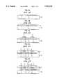
- FIG. 1Aa semiconductor layer is deposited on a transparent insulating substrate 100, and patterned to form an active layer 1. Impurities are doped into a predetermined portion of the active layer 1 to form an impurity-doped semiconductor layer 2. Then, as shown in FIG. 1B, an insulating layer 5 is formed on the overall surface of the substrate 100 including the active layer 1 and the impurity-doped layer 2. A conductive layer, such as a doped polysilicon layer or a silicide layer, is formed on the insulating layer 5 and patterned to form a gate electrode 3 and a storage electrode 4.
- a conductive layersuch as a doped polysilicon layer or a silicide layer
- Impuritiesare ion-implanted into a portion of the active layer 1 to form source and drain regions, which are indicated by a new portion of the impurity-doped semiconductor layer 2 shown in FIG. 1C.
- a portion of the insulating layer located below the gate electrode 3serves as a gate insulating layer 5 for the TFT.
- the other portion of the insulating layer located below the storage electrode 4serves as a dielectric layer 6 for a storage capacitor.
- the gate insulating layer 5 and the dielectric layer 6are formed in the same step. Accordingly, they have the same thickness and dielectric constants.
- an interlayer insulating layer 7is formed on the overall surface of the substrate.
- the interlayer insulating layer 7 and the dielectric layer 6 and/or the gate insulating layer 5are selectively etched to form contact holes exposing a portion of the impurity-doped semiconductor layer 2.
- a conductive layeris formed on the overall surface of the substrate and patterned to form a source electrode 8 and a drain electrode 9, which are connected to the impurity-doped semiconductor layer 2 through the contact holes.
- a passivation layer 10is formed on the overall surface of the substrate, and selectively etched to form a contact hole which exposes a portion of the drain electrode 9.
- a transparent conductive layeris formed on the passivation layer 10 and patterned to form a pixel electrode 11. The pixel electrode 11 is connected to the drain electrode 9 through the contact hole, thereby completing a thin film transistor having a storage capacitor.
- the dielectric layer 6needs to be made thinner, or formed of a material having a dielectric constant larger.
- the gate insulating layer and dielectric layerare formed of the same layer, they have the same thickness and dielectric constants. Accordingly, only a limited adjustment of the thickness has been possible. Also, it has been impossible to form the dielectric layer 6 using a material having a dielectric constant larger than that of the gate insulating layer.
- the present inventionis directed to a liquid crystal display that substantially obviates one or more of the problems due to limitations and disadvantages of the related art.
- An object of the present inventionis to provide a thin film transistor liquid crystal display and a method for fabricating the same that improve the numerical aperture of an LCD.
- the liquid crystal displayincludes a plurality of gate lines, a plurality of data lines in intersection with the plurality of gate lines, a plurality of thin film transistors consisting of gate insulating layers and gate electrodes formed at the respective intersections of the gate lines and data lines, channel regions, and source and drain electrodes, pixel electrodes connected to the respective drain electrodes of the respective thin film transistors, and a dielectric layer formed between the pixel electrodes and storage electrodes, in which the thickness of the gate insulating layer and the dielectric layer placed between the pixel electrode and the storage electrode are different from each other.
- the method for fabricating a liquid crystal displayincludes the steps of forming a semiconductor layer on a transparent insulating substrate, forming a gate insulating layer on the transparent insulating substrate and the semiconductor layer, forming a gate electrode on the gate insulating layer, selectively etching the gate insulating layer to be left under the gate electrode, forming a dielectric layer for storage capacitance on the transparent substrate, and forming a storage electrode on the dielectric layer.
- the method for fabricating a liquid crystal displaycomprises the steps of forming an active layer on a transparent insulating substrate, forming an impurity-doped layer in a portion of the active layer, forming a gate insulating layer on the overall surface of the substrate on which the active layer is formed, forming a gate electrode on the gate insulating layer, selectively etching the gate insulating layer to be left under the gate electrode, forming a dielectric layer for storage capacitance on the substrate, selectively doping impurities into a predetermined portion of the active layer, forming an interlevel insulating layer on the overall surface of the substrate, selectively removing the interlevel insulating layer and the dielectric layer to form a first contact hole which exposes the impurity-doped layer, forming source and drain electrodes connected to the impurity-doped layer through the first contact hole, forming a passivation layer on the overall surface of the substrate; selectively etching the passivation layer to form a second contact hole
- FIGS. 1A to 1Eare cross-sectional views showing a conventional method for fabricating a TFT for LCD
- FIGS. 2A to 2Eare cross-sectional views showing a method for fabricating a TFT for LCD according to a first embodiment of the present invention
- FIGS. 3A to 3Eare cross-sectional views showing a method for fabricating a TFT for LCD according to a second embodiment of the present invention.
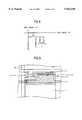
- FIG. 4is an equivalent circuit of a TFT according to the second embodiment of the present invention.
- FIG. 5is a plan view of a TFT according to the second embodiment of the present invention.
- FIG. 6is a cross-sectional view of a TFT for LCD according to a third embodiment of the present invention.
- FIG. 7is a cross-sectional view of a TFT for LCD according to a fourth embodiment of the present invention.
- FIGS. 8A to 8Dare cross-sectional views showing a method for fabricating a TFT according to a fifth embodiment of the present invention.
- a dielectric layer for a storage capacitor and a gate insulating layerare formed by different steps.
- the dielectric layercan be formed of a material having a larger dielectric constant, or formed thinner than the gate-insulating layer. Accordingly, it becomes possible to reduce the area occupied by the storage capacitor without sacrificing the capacitance, hence improving the aperture ratio of LCD.
- an interlayer insulating layer interposed between a storage electrode and a drain electrodecan also be used for a second storage capacitor.
- the second storage capacitoris connected to the first storage capacitor in parallel so as to increase the total capacitance. This makes it possible to reduce the area occupied by the storage capacitor into roughly half, thereby drastically increasing the aperture ratio of LCD.
- a semiconductor layeris deposited on a transparent insulating substrate 100, and patterned to form an active layer 1. Impurities are doped into a predetermined portion of active layer 1 to form an impurity-doped semiconductor layer 2. Then, a gate insulating layer 5 is formed on the overall surface of the substrate including the active layer 1 and the impurity doped layer 2.
- a conductive layerfor example, a metal layer, doped polysilicon layer, or silicide layer, is formed on the gate insulating layer 5 and patterned to form a gate electrode 3.
- the gate insulating layer 5is selectively etched using the gate electrode 3 as a mask. Then, as shown in FIG. 2C, a dielectric layer 6 is formed over the substrate. A conductive layer is deposited thereon and patterned to form a storage electrode 4. High-concentration impurities are doped into a predetermined portion of the active layer 1 to form source and drain regions, which are indicated by a new part of impurity-doped semiconductor layer 2 shown in FIG. 2C.
- the dielectric layer 6 together with the impurity-doped semiconductor layer 2 and the storage electrode 4constitutes a storage capacitor.
- the dielectric layer 6is formed of a material having a dielectric constant larger than that of gate insulating layer 5. This material, for example, includes SiNx, Ti oxide, Ta oxide, barium titanate oxide, and PZT oxide. Thus, the capacitance of the storage capacitor is increased.
- an interlayer insulating layer 7is deposited on the overall surface of the substrate.
- the interlayer insulating layer 7 and the dielectric layer 6are selectively etched to form contact holes which expose portions of impurity-doped semiconductor layer 2.
- a conductive layeris deposited on the overall surface of the substrate and patterned to form source and drain electrodes 8 and 9 which contact the impurity-doped semiconductor layer 2 through the contact holes.
- a passivation layer 10is deposited on the overall surface of the substrate, and then selectively etched to form a contact hole which exposes the drain electrode 9. Then, a transparent conductive layer is formed over the substrate and patterned to form a pixel electrode 11. The pixel electrode 11 is connected to drain electrode 9 through the contact hole, thereby completing the fabrication of a TFT for TFT LCD having a storage capacitor.
- a semiconductor layeris deposited on a transparent insulating substrate 100, and patterned to form an active layer 1. Impurities are doped into a predetermined portion of active layer 1 to form an impurity-doped semiconductor layer 2.
- a gate insulating layer 5is deposited on the overall surface of the substrate including the active layer 1 and the impurity-doped semiconductor layer 2.
- a conductive layerfor example, a doped polysilicon layer or silicide layer, is deposited on gate insulating layer 5, and patterned to form a gate electrode 3.
- the gate insulating layer 5is selectively etched using gate electrode 3 as a mask.
- a dielectric layer 6is deposited over the substrate.
- a conductive layeris formed thereon and patterned to form a storage electrode 4.
- High-concentration impuritiesare doped into a portion of the active layer 1 to form source and drain regions, which are indicated by a new portion of the impurity-doped semiconductor layer 2 shown in FIG. 3C.
- the dielectric layer 6 together with the impurity-doped semiconductor layer 2 and the storage electrode 4constitutes a first storage capacitor.
- the dielectric layer 6is formed of a material having a dielectric constant larger than that of gate insulating layer 5. This material includes SiNx, Ti oxide, Ta oxide, barium titanate oxide, and PZT oxide. Thus, the capacitance of the storage capacitor is increased.
- an interlayer insulating layer 7is formed on the overall surface of the substrate.
- the interlayer insulating layer 7 and the dielectric layer 6are selectively etched to form contact holes which expose portions of the impurity-doped semiconductor layer 2.
- a conductive layeris formed on the overall surface of the substrate, and patterned to form source and drain electrodes 8 and 9, which are connected to the impurity-doped semiconductor layer 2 through the contact holes.
- the drain electrode 9is formed in such a way that it overlaps the storage electrode 4.
- the interlayer insulating layer 7 together with the drain electrode 9 and the storage electrode 4constitutes a second storage capacitor.
- this storage capacitoris connected to the first storage capacitor in parallel through the storage electrode 4.
- the total capacitancebecomes roughly double, which makes it possible to reduce the area of the storage capacitance into roughly half without changing the capacitance.
- a passivation layer 10is formed on the overall surface of the substrate, and selectively etched to form a contact hole which exposes a portion of drain electrode 9. Then, a transparent conductive layer is formed on the substrate, and patterned to form a pixel electrode 11. The pixel electrode 11 is connected to the drain electrode 9 through the contact hole, finishing fabrication of a thin film transistor having a storage capacitor.
- FIG. 4is an equivalent circuit of TFT in FIG. 3E. This shows that the first and second storage capacitors A and B are connected in parallel to each other.
- FIG. 5is a plan view of TFT in FIG. 3E. As shown in FIG. 5, drain electrode 9 overlaps storage electrode 4 so that the storage capacitance can be increased due to the parallel connection of the two storage capacitors, as described above.
- a TFT for LCD according to a third embodiment of the present inventionwill be explained below with reference to FIG. 6.
- the TFT shown in FIG. 6uses the parallel connection structure of the storage capacitors according to the second embodiment of the present invention, and employs a lightly doped drain (LDD) structure.
- LDDlightly doped drain
- an LDD region 20(or an undoped offset region may be used) is formed on both sides of active layer 1.
- the same reference numeralsdesignate similar parts as in the second embodiment.
- FIG. 7is a cross-sectional view of a TFT for LCD according to a fourth embodiment of the present invention.
- the interlayer insulating layer 7 and passivation layer 10 placed above the storage electrode 4are selectively removed to connect the storage electrode 4 to the pixel electrode 11.
- the same reference numeralsare employed to designate similar parts as in the second embodiment of the present invention.
- a portion of the impurity-doped semiconductor layer 2, which is located below the storage electrode 4is electrically isolated from source and drain regions of the TFT. A method for fabricating the TFT according to the fourth embodiment of the present invention will be explained below.
- the passivation layer 10 and interlayer insulating layer 7are selectively etched to form contact holes which exposes drain electrode 9 and storage electrode 4. Then, a transparent conductive layer is formed over the substrate and patterned to form a pixel electrode 11, which contacts drain electrode 9 and storage electrode 4 through the contact holes.
- FIGS. 8A to 8Dare cross-sectional views showing a method for fabricating a bottom gate-type TFT according to a fifth embodiment of the present invention.
- a conductive layeris deposited on a substrate 100 and patterned to form a gate electrode 3 and a storage electrode 4.
- an insulating layeris deposited on the substrate and selectively etched to form a gate insulating layer 5 on a predetermined portion of the substrate including the gate electrode 3.
- a dielectric layer 6is formed on the substrate.
- the dielectric layer 6is formed of a material having a large dielectric constant, for example, Ti oxide, Ta oxide, barium titanate oxide, or PZT oxide.
- a semiconductor layeris deposited on dielectric layer 6 and patterned to form an active layer 1.
- an etch stopper 12is formed only on a portion of the active layer 1 over the gate electrode 3, and then an impurity-doped semiconductor layer 2 is formed over the substrate.
- a conductive layeris deposited on the overall surface of the substrate and patterned to form source and drain electrodes 8 and 9. An exposed portion of the impurity-doped semiconductor layer 2 is selectively removed.
- a passivation layer 10is deposited on the overall surface of the substrate, thereby finishing the process.
- the gate insulating layer of the thin film transistor and the dielectric layerare formed by different steps. Accordingly, it is possible to form the dielectric layer of a material having a larger dielectric constant or to make the dielectric layer thinner as desired. Namely, the capacitance of the storage capacitor can be adjusted without affecting the gate insulating layer of a TFT. This makes it possible to decreases the area occupied by the storage capacitor without changing the capacitance. Thus, the aperture ratio of the LCD is improved.
- the interlayer insulating layer placed between the storage electrode and the drain electrodecan be used as a second storage capacitor.
- the total capacitancecan be increased by the parallel connection of the storage capacitors. Therefore, it becomes possible to further reduce the area occupied by the storage capacitor to about one-half. This further improves the aperture ratio.
- the present inventionprovides a TFT-LCD device and a method for fabricating the same in which the storage capacitance is increased by reducing the thickness of a dielectric layer, forming the dielectric layer with a material having a larger dielectric constant, and/or connecting storage capacitors in parallel to reduce the area occupied by the storage capacitors without decreasing the storage capacitance value, thereby improving the aperture ratio of the TFT-LCD.
Landscapes
- Physics & Mathematics (AREA)
- Nonlinear Science (AREA)
- Engineering & Computer Science (AREA)
- Microelectronics & Electronic Packaging (AREA)
- Mathematical Physics (AREA)
- Chemical & Material Sciences (AREA)
- Crystallography & Structural Chemistry (AREA)
- General Physics & Mathematics (AREA)
- Optics & Photonics (AREA)
- Power Engineering (AREA)
- Liquid Crystal (AREA)
- Thin Film Transistor (AREA)
Abstract
Description
Claims (15)
Priority Applications (1)
| Application Number | Priority Date | Filing Date | Title |
|---|---|---|---|
| US09/282,162US6133967A (en) | 1995-09-12 | 1999-03-31 | Method of fabricating liquid crystal display with increased aperture ratio |
Applications Claiming Priority (2)
| Application Number | Priority Date | Filing Date | Title |
|---|---|---|---|
| KR95-29678 | 1995-09-12 | ||
| KR1019950029678AKR100205388B1 (en) | 1995-09-12 | 1995-09-12 | LCD and its manufacturing method |
Related Child Applications (1)
| Application Number | Title | Priority Date | Filing Date |
|---|---|---|---|
| US09/282,162DivisionUS6133967A (en) | 1995-09-12 | 1999-03-31 | Method of fabricating liquid crystal display with increased aperture ratio |
Publications (1)
| Publication Number | Publication Date |
|---|---|
| US5942310Atrue US5942310A (en) | 1999-08-24 |
Family
ID=19426518
Family Applications (2)
| Application Number | Title | Priority Date | Filing Date |
|---|---|---|---|
| US08/712,316Expired - LifetimeUS5942310A (en) | 1995-09-12 | 1996-09-11 | Liquid crystal display with increased aperture ratio |
| US09/282,162Expired - LifetimeUS6133967A (en) | 1995-09-12 | 1999-03-31 | Method of fabricating liquid crystal display with increased aperture ratio |
Family Applications After (1)
| Application Number | Title | Priority Date | Filing Date |
|---|---|---|---|
| US09/282,162Expired - LifetimeUS6133967A (en) | 1995-09-12 | 1999-03-31 | Method of fabricating liquid crystal display with increased aperture ratio |
Country Status (2)
| Country | Link |
|---|---|
| US (2) | US5942310A (en) |
| KR (1) | KR100205388B1 (en) |
Cited By (16)
| Publication number | Priority date | Publication date | Assignee | Title |
|---|---|---|---|---|
| EP1139454A2 (en)* | 2000-03-27 | 2001-10-04 | Sel Semiconductor Energy Laboratory Co., Ltd. | Electro-optical device |
| US6380561B1 (en)* | 1998-04-27 | 2002-04-30 | Semiconductor Energy Laboratory Co., Ltd. | Semiconductor device and process for producing the same |
| US6593592B1 (en)* | 1999-01-29 | 2003-07-15 | Semiconductor Energy Laboratory Co., Ltd. | Semiconductor device having thin film transistors |
| EP1353382A2 (en)* | 2002-04-03 | 2003-10-15 | General Electric Company | Imaging array and methods for fabricating same |
| US20030213959A1 (en)* | 2002-05-15 | 2003-11-20 | Au Optronics Corp. | Active matrix substrate for a liquid crystal display and method of forming the same |
| US20040056296A1 (en)* | 2000-01-26 | 2004-03-25 | Semiconductor Energy Laboratory Co., Ltd. | Semiconductor device and method of manufacturing the semiconductor device |
| US20040160542A1 (en)* | 1999-06-02 | 2004-08-19 | Nec Lcd Technologies, Ltd. | Process for fabrication of a liquid crystal display with thin film transistor array free from short-circuit |
| US6812975B2 (en)* | 1999-05-24 | 2004-11-02 | Fujitsu Display Technologies Corporation | Active matrix type display |
| US6906347B2 (en)* | 1999-01-11 | 2005-06-14 | Semiconductor Energy Laboratory Co., Ltd. | Semiconductor device and manufacturing method thereof |
| US20050161673A1 (en)* | 2001-12-20 | 2005-07-28 | Fujitsu Display Technologies Corporation | Thin film transistor device and method of manufacturing the same, and liquid crystal display device |
| US20060050191A1 (en)* | 2004-09-09 | 2006-03-09 | Park Yong I | Liquid crystal display device and fabrication method thereof |
| US7122835B1 (en) | 1999-04-07 | 2006-10-17 | Semiconductor Energy Laboratory Co., Ltd. | Electrooptical device and a method of manufacturing the same |
| CN100353248C (en)* | 2005-07-04 | 2007-12-05 | 友达光电股份有限公司 | Pixel structure and manufacturing method thereof |
| US20110115006A1 (en)* | 2009-11-13 | 2011-05-19 | Seiko Epson Corporation | Substrate for semiconductor device, method for producing the same, semiconductor device, and electronic apparatus |
| USRE46035E1 (en)* | 2005-09-15 | 2016-06-21 | Samsung Display Co., Ltd. | Liquid crystal display having a reduced number of data driving circuit chips |
| US11538834B2 (en)* | 2019-03-15 | 2022-12-27 | Samsung Display Co., Ltd. | Display device |
Families Citing this family (28)
| Publication number | Priority date | Publication date | Assignee | Title |
|---|---|---|---|---|
| US5917563A (en)* | 1995-10-16 | 1999-06-29 | Sharp Kabushiki Kaisha | Liquid crystal display device having an insulation film made of organic material between an additional capacity and a bus line |
| JP3270361B2 (en)* | 1997-06-09 | 2002-04-02 | 日本電気株式会社 | Thin film transistor array and method of manufacturing the same |
| JP3943245B2 (en)* | 1997-09-20 | 2007-07-11 | 株式会社半導体エネルギー研究所 | Semiconductor device |
| KR100312753B1 (en)* | 1998-10-13 | 2002-04-06 | 윤종용 | Wide viewing angle liquid crystal display device |
| KR20000039802A (en)* | 1998-12-16 | 2000-07-05 | 김영환 | Method for manufacturing lower substrate of thin film transistor liquid crystal display device |
| US6917280B1 (en)* | 1999-12-29 | 2005-07-12 | Bellsouth Intellectual Property Corporation | Cradle for accepting portable communications device and coupling portable communications device to first network by way of second network |
| US20020113268A1 (en)* | 2000-02-01 | 2002-08-22 | Jun Koyama | Nonvolatile memory, semiconductor device and method of manufacturing the same |
| KR100361467B1 (en)* | 2000-02-24 | 2002-11-21 | 엘지.필립스 엘시디 주식회사 | Thin Film Transistor Substrate of Liquid Crystal Display |
| JP2002040486A (en) | 2000-05-19 | 2002-02-06 | Seiko Epson Corp | Electro-optical device, method for manufacturing the same, and electronic apparatus |
| KR100751177B1 (en)* | 2000-08-08 | 2007-08-22 | 엘지.필립스 엘시디 주식회사 | Liquid crystal display device and manufacturing method thereof |
| KR100726132B1 (en)* | 2000-10-31 | 2007-06-12 | 엘지.필립스 엘시디 주식회사 | Array substrate for liquid crystal display device and manufacturing method |
| KR100404225B1 (en)* | 2000-12-28 | 2003-11-01 | 엘지.필립스 엘시디 주식회사 | Liquid crystal display device and method for manufacturing the same |
| US6731572B2 (en)* | 2001-04-12 | 2004-05-04 | Samsung Electronics Co., Ltd. | Optical pickup actuator, optical pickup employing the optical pickup actuator, and optical recording and/or reproducing apparatus employing the optical pickup |
| KR100491143B1 (en)* | 2001-12-26 | 2005-05-24 | 삼성에스디아이 주식회사 | Flat Panel Display with Black Matrix and Method for fabricating the Same |
| KR100869736B1 (en)* | 2001-12-29 | 2008-11-21 | 엘지디스플레이 주식회사 | LCD and its manufacturing method |
| KR20030073878A (en)* | 2002-03-13 | 2003-09-19 | 최종선 | Active Matrix Liquid Crystal Display Using Ferroelectric Switching Device |
| US6800510B2 (en) | 2002-11-06 | 2004-10-05 | Hannstar Display Corporation | Method of controlling storage capacitor's capacitance of thin film transistor liquid crystal display |
| US7190000B2 (en) | 2003-08-11 | 2007-03-13 | Samsung Electronics Co., Ltd. | Thin film transistor array panel and manufacturing method thereof |
| KR101026797B1 (en) | 2003-08-11 | 2011-04-04 | 삼성전자주식회사 | Thin film transistor array panel and manufacturing method thereof |
| US7652321B2 (en)* | 2004-03-08 | 2010-01-26 | Semiconductor Energy Laboratory Co., Ltd. | Semiconductor device and manufacturing method of the same |
| KR20050098631A (en)* | 2004-04-08 | 2005-10-12 | 삼성전자주식회사 | Liquid crystal display and panel for the same |
| KR101056013B1 (en)* | 2004-08-03 | 2011-08-10 | 엘지디스플레이 주식회사 | Manufacturing method of array substrate for liquid crystal display device |
| JP2006098641A (en)* | 2004-09-29 | 2006-04-13 | Seiko Epson Corp | Thin film semiconductor device, electro-optical device, and electronic apparatus |
| TWI257646B (en)* | 2005-09-05 | 2006-07-01 | Innolux Display Corp | Thin film transistor array substrate and method of manufacturing the same |
| US8212953B2 (en) | 2005-12-26 | 2012-07-03 | Semiconductor Energy Laboratory Co., Ltd. | Semiconductor device and method for manufacturing the same |
| DE102006060734B4 (en)* | 2006-06-30 | 2014-03-06 | Lg Display Co., Ltd. | Liquid crystal display and method for its production |
| KR101404439B1 (en) | 2007-06-29 | 2014-06-10 | 가부시키가이샤 한도오따이 에네루기 켄큐쇼 | A memory device and electronic apparatus |
| KR102284754B1 (en)* | 2014-10-27 | 2021-08-03 | 삼성디스플레이 주식회사 | Thin film transistor array substrate and organic light-emitting display including the same |
Citations (9)
| Publication number | Priority date | Publication date | Assignee | Title |
|---|---|---|---|---|
| US5054887A (en)* | 1988-08-10 | 1991-10-08 | Sharp Kabushiki Kaisha | Active matrix type liquid crystal display |
| US5182661A (en)* | 1990-06-25 | 1993-01-26 | Nec Corporation | Thin film field effect transistor array for use in active matrix liquid crystal display |
| US5474942A (en)* | 1982-04-30 | 1995-12-12 | Seiko Epson Corporation | Method of forming a liquid crystal display device |
| US5483082A (en)* | 1992-12-28 | 1996-01-09 | Fujitsu Limited | Thin film transistor matrix device |
| US5576858A (en)* | 1991-10-14 | 1996-11-19 | Hosiden Corporation | Gray scale LCD control capacitors formed between a control capacitor electrode on one side of an insulating layer and two subpixel electrodes on the other side |
| US5648663A (en)* | 1985-08-05 | 1997-07-15 | Canon Kabushiki Kaisha | Semiconductor structure having transistor and other elements on a common substrate and process for producing the same |
| US5650637A (en)* | 1982-04-30 | 1997-07-22 | Seiko Epson Corporation | Active matrix assembly |
| US5677547A (en)* | 1982-04-30 | 1997-10-14 | Seiko Epson Corporation | Thin film transistor and display device including same |
| US5691793A (en)* | 1992-07-15 | 1997-11-25 | Kabushiki Kaisha Toshiba | Liquid crystal display apparatus having gap adjusting means under the sealing region |
Family Cites Families (3)
| Publication number | Priority date | Publication date | Assignee | Title |
|---|---|---|---|---|
| JP2653099B2 (en)* | 1988-05-17 | 1997-09-10 | セイコーエプソン株式会社 | Active matrix panel, projection display and viewfinder |
| JP2622183B2 (en)* | 1990-04-05 | 1997-06-18 | シャープ株式会社 | Active matrix display device |
| KR100359795B1 (en)* | 1995-08-22 | 2003-01-14 | 엘지.필립스 엘시디 주식회사 | LCD and its manufacturing method |
- 1995
- 1995-09-12KRKR1019950029678Apatent/KR100205388B1/ennot_activeExpired - Lifetime
- 1996
- 1996-09-11USUS08/712,316patent/US5942310A/ennot_activeExpired - Lifetime
- 1999
- 1999-03-31USUS09/282,162patent/US6133967A/ennot_activeExpired - Lifetime
Patent Citations (12)
| Publication number | Priority date | Publication date | Assignee | Title |
|---|---|---|---|---|
| US5474942A (en)* | 1982-04-30 | 1995-12-12 | Seiko Epson Corporation | Method of forming a liquid crystal display device |
| US5573959A (en)* | 1982-04-30 | 1996-11-12 | Seiko Epson Corporation | Method of forming a liquid crystal device |
| US5650637A (en)* | 1982-04-30 | 1997-07-22 | Seiko Epson Corporation | Active matrix assembly |
| US5677547A (en)* | 1982-04-30 | 1997-10-14 | Seiko Epson Corporation | Thin film transistor and display device including same |
| US5648663A (en)* | 1985-08-05 | 1997-07-15 | Canon Kabushiki Kaisha | Semiconductor structure having transistor and other elements on a common substrate and process for producing the same |
| US5686326A (en)* | 1985-08-05 | 1997-11-11 | Canon Kabushiki Kaisha | Method of making thin film transistor |
| US5054887A (en)* | 1988-08-10 | 1991-10-08 | Sharp Kabushiki Kaisha | Active matrix type liquid crystal display |
| US5182661A (en)* | 1990-06-25 | 1993-01-26 | Nec Corporation | Thin film field effect transistor array for use in active matrix liquid crystal display |
| US5576858A (en)* | 1991-10-14 | 1996-11-19 | Hosiden Corporation | Gray scale LCD control capacitors formed between a control capacitor electrode on one side of an insulating layer and two subpixel electrodes on the other side |
| US5691793A (en)* | 1992-07-15 | 1997-11-25 | Kabushiki Kaisha Toshiba | Liquid crystal display apparatus having gap adjusting means under the sealing region |
| US5483082A (en)* | 1992-12-28 | 1996-01-09 | Fujitsu Limited | Thin film transistor matrix device |
| US5580796A (en)* | 1992-12-28 | 1996-12-03 | Fujitsu Limited | Method for fabricating thin film transistor matrix device |
Cited By (35)
| Publication number | Priority date | Publication date | Assignee | Title |
|---|---|---|---|---|
| US6380561B1 (en)* | 1998-04-27 | 2002-04-30 | Semiconductor Energy Laboratory Co., Ltd. | Semiconductor device and process for producing the same |
| US6552362B2 (en) | 1998-04-27 | 2003-04-22 | Semiconductor Energy Laboratory Co., Ltd. | Semiconductor device and process for producing the same |
| US6906347B2 (en)* | 1999-01-11 | 2005-06-14 | Semiconductor Energy Laboratory Co., Ltd. | Semiconductor device and manufacturing method thereof |
| US7473968B2 (en) | 1999-01-11 | 2009-01-06 | Semiconductor Energy Laboratory Co., Ltd. | Semiconductor device including a thin film transistor and a storage capacitor |
| US20050253148A1 (en)* | 1999-01-11 | 2005-11-17 | Semiconductor Energy Laboratory Co., Ltd. | Semiconductor device and manufacturing method thereof |
| US6955953B2 (en) | 1999-01-29 | 2005-10-18 | Semiconductor Energy Laboratory Co., Ltd. | Method of manufacturing a semiconductor device having thin film transistor and capacitor |
| US20040029338A1 (en)* | 1999-01-29 | 2004-02-12 | Semiconductor Energy Laboratory Co., Ltd. | Semiconductor device and method of fabricating the same |
| US6593592B1 (en)* | 1999-01-29 | 2003-07-15 | Semiconductor Energy Laboratory Co., Ltd. | Semiconductor device having thin film transistors |
| US7575961B2 (en) | 1999-04-07 | 2009-08-18 | Semiconductor Energy Laboratory Co., Ltd. | Electrooptical device and a method of manufacturing the same |
| US20070026583A1 (en)* | 1999-04-07 | 2007-02-01 | Semiconductor Energy Laboratory Co., Ltd. | Electrooptical device and a method of manufacturing the same |
| US7122835B1 (en) | 1999-04-07 | 2006-10-17 | Semiconductor Energy Laboratory Co., Ltd. | Electrooptical device and a method of manufacturing the same |
| US6812975B2 (en)* | 1999-05-24 | 2004-11-02 | Fujitsu Display Technologies Corporation | Active matrix type display |
| US6781644B1 (en)* | 1999-06-02 | 2004-08-24 | Nec Lcd Technologies, Ltd. | Liquid crystal display with thin film transistor array free from short-circuit and process for fabrication thereof |
| US20040160542A1 (en)* | 1999-06-02 | 2004-08-19 | Nec Lcd Technologies, Ltd. | Process for fabrication of a liquid crystal display with thin film transistor array free from short-circuit |
| US7081930B2 (en) | 1999-06-02 | 2006-07-25 | Nec Lcd Technologies, Ltd. | Process for fabrication of a liquid crystal display with thin film transistor array free from short-circuit |
| US20040056296A1 (en)* | 2000-01-26 | 2004-03-25 | Semiconductor Energy Laboratory Co., Ltd. | Semiconductor device and method of manufacturing the semiconductor device |
| US7365386B2 (en) | 2000-01-26 | 2008-04-29 | Semiconductor Energy Laboratory Co., Ltd. | Semiconductor device and method of manufacturing the semiconductor device |
| EP1139454A2 (en)* | 2000-03-27 | 2001-10-04 | Sel Semiconductor Energy Laboratory Co., Ltd. | Electro-optical device |
| US7700495B2 (en) | 2001-12-20 | 2010-04-20 | Sharp Kabushiki Kaisha | Thin film transistor device and method of manufacturing the same, and liquid crystal display device |
| US20050161673A1 (en)* | 2001-12-20 | 2005-07-28 | Fujitsu Display Technologies Corporation | Thin film transistor device and method of manufacturing the same, and liquid crystal display device |
| EP1353382A2 (en)* | 2002-04-03 | 2003-10-15 | General Electric Company | Imaging array and methods for fabricating same |
| US20030213959A1 (en)* | 2002-05-15 | 2003-11-20 | Au Optronics Corp. | Active matrix substrate for a liquid crystal display and method of forming the same |
| US6825497B2 (en)* | 2002-05-15 | 2004-11-30 | Au Optronics Corp. | Active matrix substrate for a liquid crystal display and method of forming the same |
| US20050019970A1 (en)* | 2002-05-15 | 2005-01-27 | Au Optronics Corp. | Active matrix substrate for a liquid crystal display and method of forming the same |
| US6927087B2 (en) | 2002-05-15 | 2005-08-09 | Au Optronics Corp. | Active matrix substrate for a liquid crystal display and method of forming the same |
| US20060050191A1 (en)* | 2004-09-09 | 2006-03-09 | Park Yong I | Liquid crystal display device and fabrication method thereof |
| US7612836B2 (en)* | 2004-09-09 | 2009-11-03 | Lg Display Co., Ltd. | Liquid crystal display device and fabrication method thereof |
| US20100014013A1 (en)* | 2004-09-09 | 2010-01-21 | Yong In Park | Liquid crystal display device and fabrication method thereof |
| US8049830B2 (en) | 2004-09-09 | 2011-11-01 | Lg Display Co., Ltd. | Liquid crystal display device and fabrication method thereof |
| CN100353248C (en)* | 2005-07-04 | 2007-12-05 | 友达光电股份有限公司 | Pixel structure and manufacturing method thereof |
| USRE46035E1 (en)* | 2005-09-15 | 2016-06-21 | Samsung Display Co., Ltd. | Liquid crystal display having a reduced number of data driving circuit chips |
| USRE47431E1 (en) | 2005-09-15 | 2019-06-11 | Samsung Display Co., Ltd. | Liquid crystal display having a reduced number of data driving circuit chips |
| US20110115006A1 (en)* | 2009-11-13 | 2011-05-19 | Seiko Epson Corporation | Substrate for semiconductor device, method for producing the same, semiconductor device, and electronic apparatus |
| US11538834B2 (en)* | 2019-03-15 | 2022-12-27 | Samsung Display Co., Ltd. | Display device |
| US12261177B2 (en) | 2019-03-15 | 2025-03-25 | Samsung Display Co., Ltd. | Display device |
Also Published As
| Publication number | Publication date |
|---|---|
| US6133967A (en) | 2000-10-17 |
| KR970016712A (en) | 1997-04-28 |
| KR100205388B1 (en) | 1999-07-01 |
Similar Documents
| Publication | Publication Date | Title |
|---|---|---|
| US5942310A (en) | Liquid crystal display with increased aperture ratio | |
| JP3654474B2 (en) | Matrix array of active matrix liquid crystal display device, liquid crystal display device and manufacturing method thereof | |
| US5793460A (en) | Liquid crystal display device and method for manufacturing the same | |
| JP4180575B2 (en) | Liquid crystal display device and method of manufacturing liquid crystal display device | |
| US7955908B2 (en) | Thin film transistor array panel and manufacturing method thereof | |
| US6911669B2 (en) | Thin film transistor array panel | |
| US7381988B2 (en) | Array substrate for liquid crystal display device and the fabrication method of the same | |
| US6407782B1 (en) | Array substrate having color filter for liquid crystal display device and method of manufacturing the same | |
| US6057904A (en) | Insulating layer arrangements for liquid crystal display and fabricating method thereof | |
| US7755708B2 (en) | Pixel structure for flat panel display | |
| US5751020A (en) | Structure of a liquid crystal display unit having exposed channel region | |
| US6875645B2 (en) | Pixel structure and fabricating method thereof | |
| US6913957B2 (en) | Method of fabricating a thin film transistor array panelsubstrate | |
| US8093595B2 (en) | Thin film array panel and manufacturing method thereof | |
| US6589826B2 (en) | Thin film transistor and a method of forming the same | |
| US5796449A (en) | Active matrix liquid crystal display with one repair line above protective layer and one below | |
| US8279389B2 (en) | Liquid crystal display device having storage lines overlapping active layers formed of polysilicon material | |
| US6940480B2 (en) | Pixel structure | |
| KR970059801A (en) | Structure and manufacturing method of TFT-LCD (LCD) | |
| KR19980021815A (en) | LCD and its manufacturing method | |
| US6100566A (en) | Multi-layer semiconductor device and method for fabricating the same | |
| US20040105042A1 (en) | [pixel structure and fabricating method thereof] | |
| JP3537938B2 (en) | Method for manufacturing active matrix display device | |
| KR100247271B1 (en) | A liquid crystal display having a storage capacitor and manufacturing method thereof | |
| KR100212270B1 (en) | Thin film transistor and manufacture thereof |
Legal Events
| Date | Code | Title | Description |
|---|---|---|---|
| AS | Assignment | Owner name:LG ELECRONICS INC., KOREA, REPUBLIC OF Free format text:ASSIGNMENT OF ASSIGNORS INTEREST;ASSIGNOR:MOON, DAE-GYU;REEL/FRAME:008208/0570 Effective date:19960826 | |
| STCF | Information on status: patent grant | Free format text:PATENTED CASE | |
| AS | Assignment | Owner name:LG. PHILIPS LCD CO., LTD., KOREA, DEMOCRATIC PEOPL Free format text:ASSIGNMENT OF ASSIGNORS INTEREST;ASSIGNOR:LG ELECTRONICS, INC.;REEL/FRAME:010281/0291 Effective date:19990921 | |
| FEPP | Fee payment procedure | Free format text:PAYOR NUMBER ASSIGNED (ORIGINAL EVENT CODE: ASPN); ENTITY STATUS OF PATENT OWNER: LARGE ENTITY | |
| FPAY | Fee payment | Year of fee payment:4 | |
| FPAY | Fee payment | Year of fee payment:8 | |
| AS | Assignment | Owner name:LG.PHILIPS LCD CO., LTD., KOREA, REPUBLIC OF Free format text:ASSIGNMENT OF ASSIGNORS INTEREST;ASSIGNOR:LG ELECTRONICS INC.;REEL/FRAME:020385/0124 Effective date:19990921 | |
| AS | Assignment | Owner name:LG DISPLAY CO., LTD., KOREA, REPUBLIC OF Free format text:CHANGE OF NAME;ASSIGNOR:LG.PHILIPS LCD CO., LTD.;REEL/FRAME:021147/0009 Effective date:20080319 Owner name:LG DISPLAY CO., LTD.,KOREA, REPUBLIC OF Free format text:CHANGE OF NAME;ASSIGNOR:LG.PHILIPS LCD CO., LTD.;REEL/FRAME:021147/0009 Effective date:20080319 | |
| FEPP | Fee payment procedure | Free format text:PAYER NUMBER DE-ASSIGNED (ORIGINAL EVENT CODE: RMPN); ENTITY STATUS OF PATENT OWNER: LARGE ENTITY Free format text:PAYOR NUMBER ASSIGNED (ORIGINAL EVENT CODE: ASPN); ENTITY STATUS OF PATENT OWNER: LARGE ENTITY | |
| FPAY | Fee payment | Year of fee payment:12 |