US5942137A - Method and apparatus for laser scribing grooves on hard crystals - Google Patents
Method and apparatus for laser scribing grooves on hard crystalsDownload PDFInfo
- Publication number
- US5942137A US5942137AUS08/920,557US92055797AUS5942137AUS 5942137 AUS5942137 AUS 5942137AUS 92055797 AUS92055797 AUS 92055797AUS 5942137 AUS5942137 AUS 5942137A
- Authority
- US
- United States
- Prior art keywords
- crystal
- jig
- surface processing
- upstand
- vacuum
- Prior art date
- Legal status (The legal status is an assumption and is not a legal conclusion. Google has not performed a legal analysis and makes no representation as to the accuracy of the status listed.)
- Expired - Lifetime
Links
Images


Classifications
- C—CHEMISTRY; METALLURGY
- C30—CRYSTAL GROWTH
- C30B—SINGLE-CRYSTAL GROWTH; UNIDIRECTIONAL SOLIDIFICATION OF EUTECTIC MATERIAL OR UNIDIRECTIONAL DEMIXING OF EUTECTOID MATERIAL; REFINING BY ZONE-MELTING OF MATERIAL; PRODUCTION OF A HOMOGENEOUS POLYCRYSTALLINE MATERIAL WITH DEFINED STRUCTURE; SINGLE CRYSTALS OR HOMOGENEOUS POLYCRYSTALLINE MATERIAL WITH DEFINED STRUCTURE; AFTER-TREATMENT OF SINGLE CRYSTALS OR A HOMOGENEOUS POLYCRYSTALLINE MATERIAL WITH DEFINED STRUCTURE; APPARATUS THEREFOR
- C30B33/00—After-treatment of single crystals or homogeneous polycrystalline material with defined structure
- B—PERFORMING OPERATIONS; TRANSPORTING
- B23—MACHINE TOOLS; METAL-WORKING NOT OTHERWISE PROVIDED FOR
- B23K—SOLDERING OR UNSOLDERING; WELDING; CLADDING OR PLATING BY SOLDERING OR WELDING; CUTTING BY APPLYING HEAT LOCALLY, e.g. FLAME CUTTING; WORKING BY LASER BEAM
- B23K26/00—Working by laser beam, e.g. welding, cutting or boring
- B23K26/02—Positioning or observing the workpiece, e.g. with respect to the point of impact; Aligning, aiming or focusing the laser beam
- B—PERFORMING OPERATIONS; TRANSPORTING
- B23—MACHINE TOOLS; METAL-WORKING NOT OTHERWISE PROVIDED FOR
- B23K—SOLDERING OR UNSOLDERING; WELDING; CLADDING OR PLATING BY SOLDERING OR WELDING; CUTTING BY APPLYING HEAT LOCALLY, e.g. FLAME CUTTING; WORKING BY LASER BEAM
- B23K26/00—Working by laser beam, e.g. welding, cutting or boring
- B23K26/36—Removing material
- B23K26/361—Removing material for deburring or mechanical trimming
- B—PERFORMING OPERATIONS; TRANSPORTING
- B23—MACHINE TOOLS; METAL-WORKING NOT OTHERWISE PROVIDED FOR
- B23K—SOLDERING OR UNSOLDERING; WELDING; CLADDING OR PLATING BY SOLDERING OR WELDING; CUTTING BY APPLYING HEAT LOCALLY, e.g. FLAME CUTTING; WORKING BY LASER BEAM
- B23K26/00—Working by laser beam, e.g. welding, cutting or boring
- B23K26/36—Removing material
- B23K26/40—Removing material taking account of the properties of the material involved
- B—PERFORMING OPERATIONS; TRANSPORTING
- B23—MACHINE TOOLS; METAL-WORKING NOT OTHERWISE PROVIDED FOR
- B23K—SOLDERING OR UNSOLDERING; WELDING; CLADDING OR PLATING BY SOLDERING OR WELDING; CUTTING BY APPLYING HEAT LOCALLY, e.g. FLAME CUTTING; WORKING BY LASER BEAM
- B23K2103/00—Materials to be soldered, welded or cut
- B23K2103/50—Inorganic material, e.g. metals, not provided for in B23K2103/02 – B23K2103/26
- B23K2103/52—Ceramics
Definitions
- the present inventionrelates to the surface processing in general and to the scribing of grooves on hard crystals in particular.
- Hard crystalssuch as PLZT (lead lanthanum zirconate titanate) or KTN (Potassium Tantalum Neodymium) are widely used in optoelectronic storage and display devices.
- the PLZT crystalis a ferroelectric, ceramic, electrooptical material having optical properties which can be changed by an electric field or by being placed in tension or compression.
- High powered laserssuch as a carbon dioxide (CO 2 ) laser, Nd:Yag laser or Excimer laser, can be used.
- CO 2carbon dioxide
- Nd:Yag laser or Excimer lasercan be used.
- these conventional lasershave disadvantages. Even because of high absorption, the crystal becomes heated and can reach temperatures close to or even above Curie temperature. These high temperatures cause the loss of the crystal's optical properties, particularly in the region surrounding the processing area.
- Copper vapor laserare also known in the art of laser etching.
- the copper vapor laserhas an extremely high photon gain and large active aperture.
- the brittle crystalcan be "chipped" away or “crumbled” in ordered manner, confined to very small area--without heating.
- surface processingsuch as etching, drilling and cutting can be performed on a marked area as small as 2 microns.
- An object of the present inventionis to provide a method and apparatus for surface processing on small areas of hard crystals which overcome the disadvantages of prior methods.
- a further object of the present inventionis to provide a method and apparatus for accurately scribing grooves on small areas of hard crystal.
- apparatusfor positioning, holding and surface processing a small dimensioned hard crystal.
- the apparatusincludes a position location jig for positioning and locating the crystal in an x-y plane, vacuum pump means for generating a vacuum to grip the crystal in the x-y plane, copper vapor laser apparatus for surface processing the hard crystals and projection microscope apparatus mounted on the laser for accurate location of the processing area.
- the surface processingincludes scribing or drilling the crystals.
- the scribingincludes scribing symmetrical grooves on two parallel surfaces of the crystal.
- a jigfor positioning and holding a crystal during surface processing.
- the jigincludes apparatus for positioning and locating the crystal in an x-y plane and vacuum pump means for generating a vacuum to grip the crystal in the x-y plane.
- the crystalis a ferroelectric, ceramic, electrooptical material.
- the crystalincludes any of a group of crystals including PLZT (lead lanthanum zirconate titanate) and KTN (Potassium Tantalum Neodymium).
- a method for surface processing small dimensioned crystalsincludes the steps of:
- the methodfurther includes the steps of:
- the methodalso includes the steps of:
- the step of surface processingincludes the step of scribing symmetrical grooves on two parallel surfaces of the crystal.
- the crystalis gripped by vacuum apparatus during the steps of lifting, replacing and positioning.
- FIG. 1is a schematic isometric illustration of a fabricated flat crystal having a plurality of registrated channels cut into opposite faces thereof according to a preferred embodiment of the present invention
- FIG. 2is a schematic isometric illustration of a jig for supporting and holding a crystal, according to a preferred embodiment of the present invention
- FIGS. 3 and 4are plan and sectional elevation illustrations of jig of FIG. 2;
- FIG. 5is an enlarged isometric detail illustrating the use of a copper vapor laser (CVL) for surface processing on the crystal of FIG. 2;
- FIGS. 6A and 6Bare a flow chart illustration of the method for performing surface processing.
- Wafer crystalssuch as PLZT crystal
- Exemplary dimensions such crystalsare approximately between 500-700 microns width and between 200-300 microns thick, having an overall length of approximately 12-20 mm.
- FIG. 1is a schematic isometric illustration of part of a flat fabricated PLZT crystal 100 having a plurality of registered channels 102 and 103 cut into opposite faces thereof, according to a preferred embodiment of the present invention. Each segment 104 of crystal is separated by a channel 102 (or 103).
- each channel 102(and 103) is extremely small between 6 to 25 microns wide, for example. It is thus, possible to fabricate a large number of such channels (that is, over 50) in each face of a standard 12-20 mm long crystal. It will be appreciated that the dimensions are given by way of example only and without in any way limiting the scope of the invention.
- Applicants of the present inventionhave realized that, by constructing a specialized jig to correctly position a crystal in the x and y direction and simultaneously firmly holding the crystal in position, it is possible to accurately fabricate a plurality of tiny channels within a crystal without damaging the crystal.
- a plurality of registered channels 102 having exceptionally small dimensionscan be fabricated on each side of the crystal 100.
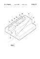
- FIG. 2is an isometric view of a jig 10 for supporting and holding a crystal 12, according to a preferred embodiment of the present invention, so as to enable surface processing work to be carried out on the crystal.
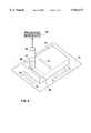
- FIGS. 3 and 4are plan and sectional elevation illustrations, respectively, of jig 10.
- Crystal 12is a standard crystal which has been prepared, by know methods, to a precise rectangular form (for example) to the required dimensions.
- a feature of the inventionis that crystal 12 can be correctly positioned in on jig 10 to allow for symmetrical processing on opposite faces of the crystal. Additionally, the crystal 12 is firmly held in that position by vacuum means.
- Jig 10is generally an inverted "T"-shaped block (when viewed from the side (FIG. 4 )), having a central upstand section 14.
- Upstand 14comprises a pair of side location pins 16a and 16b, and a central location pin 18 protruding from upstand 14.
- Central location pin 18is precisely located in the center of upstand 14, as indicated by center line, referenced 20.
- Central location pin 18precisely locates the position of the "head” of the crystal 12 so that when the crystal is turned over (for processing on the reverse side), by positioning the "head” of the crystal against the central pin 18, the crystal can be correctly located vis-a-vis the first surface.
- Upstand 14further comprises a generally rectangular channel 22 having plurality of apertures 24 formed therein.
- Channel 22is formed on top of upstand 14 and located adjacent to pins 16a and 16b and along center line 20.
- a generally cylindrical conduit 26is formed within the upstand 14, extending below and connected to the plurality of apertures 24.
- a vacuum pump(not shown) is suitably attached to conduit 26 to ensure a sealed connection.
- the crystal 12 to be worked onis placed on jig 10 in contact with side location pins 16a and 16b, and central location pin 18, thereby correctly positioning the crystal.
- a vacuumis then applied, via conduit 26 and apertures 24 to the crystal 12. The resulting suction grips the crystal 12 and prevents it from moving.
- FIG. 5is an enlarged isometric detail illustrating the use of a copper vapor laser (CVL) 50 for etching crystal 12.
- the crystal 12is tightly held in position on jig 10 (not shown) by vacuum, as described hereinabove.
- the jig 10is placed on an x-y translation stage 51 (work table)--not shown--, and moved into the precise position for processing by adjusting the table along the X-Y planes, schematically represented by arrows, referenced X 1 .-X 2 and Y 1 .-Y 2 .
- processingis carried out by a system using a projection microscope 52 and copper vapor laser 50 (CVL).
- CVLcopper vapor laser 50
- Any suitable projection microscope system using CVL which allows for a very high optical magnification of high magnitudemay be used.
- An exemplary systemis commercially available from Rotem Industries Ltd. of Beersheva, Israel.
- the projection microscopeshould be capable of magnification of approximately x5000 and the copper vapor laser should permit a 0.7 ⁇ m resolution.
- Arrow X3indicates the longitudinal movement of the translation stage 51 in relation to the static CVL during processing.
- the systemallows the operator to mark any area on the image as low as 2 ⁇ diagonal squares for surface processing.
- the CVL laserWhen the CVL laser is activated, the CVL plasma tube 54 is excited by electric discharge pulses to emit photons near the green and yellow colors to produce a laser beam 56.
- the beam 56operates to perform the surface processing, such as etching or drilling or for cutting a channel 58, as shown in FIG. 5.
- Channel 58is similar to 102 and 103 described hereinabove with respect to FIG. 1.
- channel 58(or 102) may be configured to any suitable shape and is not restricted to the semi-circular cross-section illustrated in FIG. 5.
- the vacuumis released and the crystal wafer 12 is lifted off the jig 10, preferably by a vacuum pen, such as the "air pinette” model incorporating a vacuum pad and vacuum generator, manufactured by Nihon Pisco Co. Ltd. of Okaya City, Japan, or similar and turned over for processing on the reverse face, if required.
- a vacuum pensuch as the "air pinette” model incorporating a vacuum pad and vacuum generator, manufactured by Nihon Pisco Co. Ltd. of Okaya City, Japan, or similar and turned over for processing on the reverse face, if required.
- the fabricated crystal 12is similar to the PLZT crystal 100 of FIG. 1 (described hereinabove).
- FIGS. 6A and 6Bare a flow chart illustration of the method for performing surface processing, such as etching, drilling and cutting on crystal 12.
- the method describedis based on the use of a projection microscope 52 and copper vapor laser 50 (CVL), described hereinabove with respect to FIG. 5.
- CVLcopper vapor laser 50
- the crystal 12is first fabricated to the required external dimensions (step 201). The crystal 12 is then positioned on jig 10 (step 202) so that the crystal is in contact with side location pins 16a and 16b and central location pin 18, thereby correctly positioning the crystal in the x-y plane. A vacuum is then generated applied by the vacuum pump through conduit 26 to grip the crystal (step 204).
- the jig 10 with the crystal 12 gripped in positionis placed on the x-y translation stage of the projection microscope 52 (step 206).
- the x-y translation stageis then moved into the initial working position (step 208), using the high magnification powers of the projection microscope to accurately locate the portion of the surface to be worked on.
- the copper vapor laser 54is then activated to perform the etching or cutting on the marked portion of the crystal (step 210).
- the x-y translation stageis then moved to a new working position (step 212) and surface processing step 210 is repeated (loop 213).
- the vacuum holding the crystalis released (step 214).
- the crystalis removed from the jig (step 218) by means of a vacuum pen or similar, inverted and repositioned on the jig (step 220).
- the crystalis centered by locating the "head" against the central pin 18 thereby ensuring that the crystal is correctly located vis-a-vis the first surface, so that the surface processing on the reverse surface will be aligned with the surface processing on the other surface.
- the vacuumis regenerated (step 222) and processing performed (steps 208-212 for the reverse side.
- the formed crystalis removed, preferably by means of the vacuum pen (step 224).
Landscapes
- Engineering & Computer Science (AREA)
- Physics & Mathematics (AREA)
- Optics & Photonics (AREA)
- Plasma & Fusion (AREA)
- Mechanical Engineering (AREA)
- Chemical & Material Sciences (AREA)
- Crystallography & Structural Chemistry (AREA)
- Materials Engineering (AREA)
- Metallurgy (AREA)
- Organic Chemistry (AREA)
- Crystals, And After-Treatments Of Crystals (AREA)
Abstract
Description
Claims (10)
Priority Applications (1)
| Application Number | Priority Date | Filing Date | Title |
|---|---|---|---|
| US08/920,557US5942137A (en) | 1997-08-29 | 1997-08-29 | Method and apparatus for laser scribing grooves on hard crystals |
Applications Claiming Priority (1)
| Application Number | Priority Date | Filing Date | Title |
|---|---|---|---|
| US08/920,557US5942137A (en) | 1997-08-29 | 1997-08-29 | Method and apparatus for laser scribing grooves on hard crystals |
Publications (1)
| Publication Number | Publication Date |
|---|---|
| US5942137Atrue US5942137A (en) | 1999-08-24 |
Family
ID=25443949
Family Applications (1)
| Application Number | Title | Priority Date | Filing Date |
|---|---|---|---|
| US08/920,557Expired - LifetimeUS5942137A (en) | 1997-08-29 | 1997-08-29 | Method and apparatus for laser scribing grooves on hard crystals |
Country Status (1)
| Country | Link |
|---|---|
| US (1) | US5942137A (en) |
Cited By (8)
| Publication number | Priority date | Publication date | Assignee | Title |
|---|---|---|---|---|
| US6098862A (en)* | 1998-05-18 | 2000-08-08 | Lucent Technologies Inc. | Incrementally continuous laser cleaving process |
| US6396618B1 (en) | 1999-11-03 | 2002-05-28 | The Regents Of The University Of California | Opposing electrode light modulator array and method for manufacturing the same |
| US20040031779A1 (en)* | 2002-05-17 | 2004-02-19 | Cahill Steven P. | Method and system for calibrating a laser processing system and laser marking system utilizing same |
| US6744009B1 (en) | 2002-04-02 | 2004-06-01 | Seagate Technology Llc | Combined laser-scribing and laser-breaking for shaping of brittle substrates |
| US20040104202A1 (en)* | 2000-01-28 | 2004-06-03 | Gsi Lumonics, Inc. | Laser scanning method and system for marking articles such as printed circuit boards, integrated circuits and the like |
| US6787732B1 (en) | 2002-04-02 | 2004-09-07 | Seagate Technology Llc | Method for laser-scribing brittle substrates and apparatus therefor |
| US20060108337A1 (en)* | 2004-11-11 | 2006-05-25 | Bo Gu | Method and system for laser soft marking |
| US20060189091A1 (en)* | 2004-11-11 | 2006-08-24 | Bo Gu | Method and system for laser hard marking |
Citations (9)
| Publication number | Priority date | Publication date | Assignee | Title |
|---|---|---|---|---|
| US4141456A (en)* | 1976-08-30 | 1979-02-27 | Rca Corp. | Apparatus and method for aligning wafers |
| US4869768A (en)* | 1988-07-15 | 1989-09-26 | North American Philips Corp. | Ultrasonic transducer arrays made from composite piezoelectric materials |
| US5059764A (en)* | 1988-10-31 | 1991-10-22 | Spectra-Physics, Inc. | Diode-pumped, solid state laser-based workstation for precision materials processing and machining |
| US5221989A (en)* | 1991-11-13 | 1993-06-22 | Northrop Corporation | Longitudinal plzt spatial light modulator |
| US5310990A (en)* | 1991-06-03 | 1994-05-10 | The United Stated Of America As Represented By The Secretary Of The Navy | Method of laser processing ferroelectric materials |
| JPH081367A (en)* | 1994-06-22 | 1996-01-09 | Brother Ind Ltd | Laser processing equipment |
| JPH08309576A (en)* | 1995-05-12 | 1996-11-26 | Fuji Electric Corp Res & Dev Ltd | Laser processing method |
| US5611946A (en)* | 1994-02-18 | 1997-03-18 | New Wave Research | Multi-wavelength laser system, probe station and laser cutter system using the same |
| US5744780A (en)* | 1995-09-05 | 1998-04-28 | The United States Of America As Represented By The United States Department Of Energy | Apparatus for precision micromachining with lasers |
- 1997
- 1997-08-29USUS08/920,557patent/US5942137A/ennot_activeExpired - Lifetime
Patent Citations (9)
| Publication number | Priority date | Publication date | Assignee | Title |
|---|---|---|---|---|
| US4141456A (en)* | 1976-08-30 | 1979-02-27 | Rca Corp. | Apparatus and method for aligning wafers |
| US4869768A (en)* | 1988-07-15 | 1989-09-26 | North American Philips Corp. | Ultrasonic transducer arrays made from composite piezoelectric materials |
| US5059764A (en)* | 1988-10-31 | 1991-10-22 | Spectra-Physics, Inc. | Diode-pumped, solid state laser-based workstation for precision materials processing and machining |
| US5310990A (en)* | 1991-06-03 | 1994-05-10 | The United Stated Of America As Represented By The Secretary Of The Navy | Method of laser processing ferroelectric materials |
| US5221989A (en)* | 1991-11-13 | 1993-06-22 | Northrop Corporation | Longitudinal plzt spatial light modulator |
| US5611946A (en)* | 1994-02-18 | 1997-03-18 | New Wave Research | Multi-wavelength laser system, probe station and laser cutter system using the same |
| JPH081367A (en)* | 1994-06-22 | 1996-01-09 | Brother Ind Ltd | Laser processing equipment |
| JPH08309576A (en)* | 1995-05-12 | 1996-11-26 | Fuji Electric Corp Res & Dev Ltd | Laser processing method |
| US5744780A (en)* | 1995-09-05 | 1998-04-28 | The United States Of America As Represented By The United States Department Of Energy | Apparatus for precision micromachining with lasers |
Cited By (19)
| Publication number | Priority date | Publication date | Assignee | Title |
|---|---|---|---|---|
| US6098862A (en)* | 1998-05-18 | 2000-08-08 | Lucent Technologies Inc. | Incrementally continuous laser cleaving process |
| US6396618B1 (en) | 1999-11-03 | 2002-05-28 | The Regents Of The University Of California | Opposing electrode light modulator array and method for manufacturing the same |
| US20040104202A1 (en)* | 2000-01-28 | 2004-06-03 | Gsi Lumonics, Inc. | Laser scanning method and system for marking articles such as printed circuit boards, integrated circuits and the like |
| US6787732B1 (en) | 2002-04-02 | 2004-09-07 | Seagate Technology Llc | Method for laser-scribing brittle substrates and apparatus therefor |
| US6744009B1 (en) | 2002-04-02 | 2004-06-01 | Seagate Technology Llc | Combined laser-scribing and laser-breaking for shaping of brittle substrates |
| US20060054608A1 (en)* | 2002-05-17 | 2006-03-16 | Gsi Lumonics Corporation | Method and system for calibrating a laser processing system and laser marking system utilizing same |
| US20060180580A1 (en)* | 2002-05-17 | 2006-08-17 | Gsi Lumonics Corporation | High speed, laser-based marking method and system for producing machine readable marks on workpieces and semiconductor devices with reduced subsurface damage produced thereby |
| US20040060910A1 (en)* | 2002-05-17 | 2004-04-01 | Rainer Schramm | High speed, laser-based marking method and system for producing machine readable marks on workpieces and semiconductor devices with reduced subsurface damage produced thereby |
| US20040031779A1 (en)* | 2002-05-17 | 2004-02-19 | Cahill Steven P. | Method and system for calibrating a laser processing system and laser marking system utilizing same |
| US7015418B2 (en) | 2002-05-17 | 2006-03-21 | Gsi Group Corporation | Method and system for calibrating a laser processing system and laser marking system utilizing same |
| USRE41924E1 (en)* | 2002-05-17 | 2010-11-16 | Gsi Group Corporation | Method and system for machine vision-based feature detection and mark verification in a workpiece or wafer marking system |
| US7067763B2 (en)* | 2002-05-17 | 2006-06-27 | Gsi Group Corporation | High speed, laser-based marking method and system for producing machine readable marks on workpieces and semiconductor devices with reduced subsurface damage produced thereby |
| US20040144760A1 (en)* | 2002-05-17 | 2004-07-29 | Cahill Steven P. | Method and system for marking a workpiece such as a semiconductor wafer and laser marker for use therein |
| US20070031993A1 (en)* | 2002-05-17 | 2007-02-08 | Gsi Lumonics Corporation | Method and system for machine vision-based feature detection and mark verification in a workpiece or wafer marking system |
| US20060186096A1 (en)* | 2002-05-17 | 2006-08-24 | Gsi Lumonics Corporation | High speed, laser-based marking method and system for producing machine readable marks on workpieces and semiconductor devices with reduced subsurface damage produced thereby |
| US7119351B2 (en) | 2002-05-17 | 2006-10-10 | Gsi Group Corporation | Method and system for machine vision-based feature detection and mark verification in a workpiece or wafer marking system |
| US20060189091A1 (en)* | 2004-11-11 | 2006-08-24 | Bo Gu | Method and system for laser hard marking |
| US7705268B2 (en) | 2004-11-11 | 2010-04-27 | Gsi Group Corporation | Method and system for laser soft marking |
| US20060108337A1 (en)* | 2004-11-11 | 2006-05-25 | Bo Gu | Method and system for laser soft marking |
Similar Documents
| Publication | Publication Date | Title |
|---|---|---|
| US6841482B2 (en) | Laser machining of semiconductor materials | |
| US7112518B2 (en) | Method and apparatus for cutting devices from substrates | |
| US6806544B2 (en) | Method and apparatus for cutting devices from conductive substrates secured during cutting by vacuum pressure | |
| KR100877936B1 (en) | Laser segmented cutting | |
| US6580054B1 (en) | Scribing sapphire substrates with a solid state UV laser | |
| JP5225639B2 (en) | Manufacturing method of semiconductor laser device | |
| US8263901B2 (en) | Method for laser micromachining | |
| TWI447794B (en) | Laser processing of workpieces containing low-k dielectric material | |
| US5949932A (en) | Assembly for focusing and coupling the radiation produced by a semiconductor laser into optical fibers | |
| US5942137A (en) | Method and apparatus for laser scribing grooves on hard crystals | |
| KR102399929B1 (en) | Die bonder | |
| JPH1158061A (en) | Laser beam machine for flexible material and its machining method | |
| JPH0688923A (en) | Method for matching position of optoelectronic part and optical axis of optical fiber and device using method thereof | |
| JPH06269968A (en) | Glass cutting method and device | |
| US20050118934A1 (en) | Method for shaping air bearing surface of magnetic head slider and manufacturing method of magnetic head slider | |
| US6552302B2 (en) | Method for correcting surface shape of magnetic head slider and magnetic head slider | |
| JPH05302876A (en) | Preparing method of sample for tem observation and jig for grinding | |
| JPH02132844A (en) | Method for dividing compound semiconductor wafers | |
| JPH1094892A (en) | Laser heating device | |
| JPS61199596A (en) | Micro-shape processing method and mask for micro-shape processing | |
| Khan | Laser Etching of Ceramics for Defining Slider Air-Bearing Surfaces for Magnetic Recording Heads | |
| JPH0521820A (en) | Opto-semiconductor element mounting method | |
| JPH11216624A (en) | Flexible pallets | |
| JPH08146268A (en) | Method for fixing optical parts |
Legal Events
| Date | Code | Title | Description |
|---|---|---|---|
| AS | Assignment | Owner name:SCITEX CORPORATION LTD., ISRAEL Free format text:ASSIGNMENT OF ASSIGNORS INTEREST;ASSIGNORS:KAMIR, YOSEF;RONEN, JOSEF;REEL/FRAME:008784/0878 Effective date:19970826 | |
| STCF | Information on status: patent grant | Free format text:PATENTED CASE | |
| AS | Assignment | Owner name:CREOSCITEX CORPORATION LTD., ISRAEL Free format text:ASSIGNMENT OF ASSIGNORS INTEREST;ASSIGNOR:SCITEX CORPORATION LTD.;REEL/FRAME:011716/0966 Effective date:20000911 | |
| AS | Assignment | Owner name:CREO IL LTD., ISRAEL Free format text:CHANGE OF NAME;ASSIGNOR:CREOSCITEX CORPORATION LTD.;REEL/FRAME:012944/0274 Effective date:20020217 | |
| FEPP | Fee payment procedure | Free format text:PAYOR NUMBER ASSIGNED (ORIGINAL EVENT CODE: ASPN); ENTITY STATUS OF PATENT OWNER: LARGE ENTITY | |
| FPAY | Fee payment | Year of fee payment:4 | |
| REMI | Maintenance fee reminder mailed | ||
| FEPP | Fee payment procedure | Free format text:PAYER NUMBER DE-ASSIGNED (ORIGINAL EVENT CODE: RMPN); ENTITY STATUS OF PATENT OWNER: LARGE ENTITY Free format text:PAYOR NUMBER ASSIGNED (ORIGINAL EVENT CODE: ASPN); ENTITY STATUS OF PATENT OWNER: LARGE ENTITY | |
| AS | Assignment | Owner name:KODAK I L, LTD., ISRAEL Free format text:CHANGE OF NAME;ASSIGNOR:CREO IL, LTD.;REEL/FRAME:018563/0536 Effective date:20060712 | |
| FPAY | Fee payment | Year of fee payment:8 | |
| FPAY | Fee payment | Year of fee payment:12 |