US5940732A - Method of fabricating semiconductor device - Google Patents
Method of fabricating semiconductor deviceDownload PDFInfo
- Publication number
- US5940732A US5940732AUS08/753,428US75342896AUS5940732AUS 5940732 AUS5940732 AUS 5940732AUS 75342896 AUS75342896 AUS 75342896AUS 5940732 AUS5940732 AUS 5940732A
- Authority
- US
- United States
- Prior art keywords
- insulating film
- etching
- opening
- film
- forming
- Prior art date
- Legal status (The legal status is an assumption and is not a legal conclusion. Google has not performed a legal analysis and makes no representation as to the accuracy of the status listed.)
- Expired - Lifetime
Links
Images


Classifications
- H—ELECTRICITY
- H10—SEMICONDUCTOR DEVICES; ELECTRIC SOLID-STATE DEVICES NOT OTHERWISE PROVIDED FOR
- H10D—INORGANIC ELECTRIC SEMICONDUCTOR DEVICES
- H10D30/00—Field-effect transistors [FET]
- H10D30/01—Manufacture or treatment
- H10D30/021—Manufacture or treatment of FETs having insulated gates [IGFET]
- H10D30/031—Manufacture or treatment of FETs having insulated gates [IGFET] of thin-film transistors [TFT]
- H10D30/0312—Manufacture or treatment of FETs having insulated gates [IGFET] of thin-film transistors [TFT] characterised by the gate electrodes
- H10D30/0314—Manufacture or treatment of FETs having insulated gates [IGFET] of thin-film transistors [TFT] characterised by the gate electrodes of lateral top-gate TFTs comprising only a single gate
- H—ELECTRICITY
- H01—ELECTRIC ELEMENTS
- H01L—SEMICONDUCTOR DEVICES NOT COVERED BY CLASS H10
- H01L21/00—Processes or apparatus adapted for the manufacture or treatment of semiconductor or solid state devices or of parts thereof
- H01L21/02—Manufacture or treatment of semiconductor devices or of parts thereof
- H01L21/04—Manufacture or treatment of semiconductor devices or of parts thereof the devices having potential barriers, e.g. a PN junction, depletion layer or carrier concentration layer
- H01L21/18—Manufacture or treatment of semiconductor devices or of parts thereof the devices having potential barriers, e.g. a PN junction, depletion layer or carrier concentration layer the devices having semiconductor bodies comprising elements of Group IV of the Periodic Table or AIIIBV compounds with or without impurities, e.g. doping materials
- H01L21/30—Treatment of semiconductor bodies using processes or apparatus not provided for in groups H01L21/20 - H01L21/26
- H01L21/31—Treatment of semiconductor bodies using processes or apparatus not provided for in groups H01L21/20 - H01L21/26 to form insulating layers thereon, e.g. for masking or by using photolithographic techniques; After treatment of these layers; Selection of materials for these layers
- H01L21/3105—After-treatment
- H01L21/311—Etching the insulating layers by chemical or physical means
- H01L21/31105—Etching inorganic layers
- H01L21/31111—Etching inorganic layers by chemical means
- H—ELECTRICITY
- H01—ELECTRIC ELEMENTS
- H01L—SEMICONDUCTOR DEVICES NOT COVERED BY CLASS H10
- H01L21/00—Processes or apparatus adapted for the manufacture or treatment of semiconductor or solid state devices or of parts thereof
- H01L21/70—Manufacture or treatment of devices consisting of a plurality of solid state components formed in or on a common substrate or of parts thereof; Manufacture of integrated circuit devices or of parts thereof
- H01L21/71—Manufacture of specific parts of devices defined in group H01L21/70
- H01L21/768—Applying interconnections to be used for carrying current between separate components within a device comprising conductors and dielectrics
- H01L21/76801—Applying interconnections to be used for carrying current between separate components within a device comprising conductors and dielectrics characterised by the formation and the after-treatment of the dielectrics, e.g. smoothing
- H01L21/76802—Applying interconnections to be used for carrying current between separate components within a device comprising conductors and dielectrics characterised by the formation and the after-treatment of the dielectrics, e.g. smoothing by forming openings in dielectrics
- H01L21/76804—Applying interconnections to be used for carrying current between separate components within a device comprising conductors and dielectrics characterised by the formation and the after-treatment of the dielectrics, e.g. smoothing by forming openings in dielectrics by forming tapered via holes
- H—ELECTRICITY
- H10—SEMICONDUCTOR DEVICES; ELECTRIC SOLID-STATE DEVICES NOT OTHERWISE PROVIDED FOR
- H10D—INORGANIC ELECTRIC SEMICONDUCTOR DEVICES
- H10D30/00—Field-effect transistors [FET]
- H10D30/01—Manufacture or treatment
- H10D30/021—Manufacture or treatment of FETs having insulated gates [IGFET]
- H10D30/031—Manufacture or treatment of FETs having insulated gates [IGFET] of thin-film transistors [TFT]
- H10D30/0321—Manufacture or treatment of FETs having insulated gates [IGFET] of thin-film transistors [TFT] comprising silicon, e.g. amorphous silicon or polysilicon
Definitions
- the present inventionrelates to a method of fabricating a semiconductor device, using a crystalline thin-film semiconductor and, more particularly, to a method of fabricating planar type thin-film transistors.
- TFTsthin-film transistors
- An active matrix liquid crystal displayhas millions of pixels arranged in rows and columns. TFTs are arranged at these pixels. Electric charge going in and out of each electrode at the pixels is controlled by the switching action of the TFTs.
- a circuitfor driving TFTs for displaying these pixel electrodes be formed out of TFTs integrated with the former TFTs on the same glass substrate.
- the poor contactis a main cause of premature deterioration of semiconductor device characteristics. Especially, where large currents flow or the device is operated at high temperatures, the deterioration coursed by the poor contact is promoted. Therefore, it is said that the reliability of contacts determines the reliability of the semiconductor device.
- the gate electrodesare brought out of the pixel display regions directly and so no contacts exist. That is, contact with the pixel electrodes is very important for the reliability of the liquid crystal display.
- the causes of poor contactare classified into three major categories.
- the first categoryis that a conductive film forming interconnect electrodes is not in ohmic contact with a semiconductor film forming the source/drain regions of TFTs. This is caused by formation of an insulating coating such as a metal oxide at the junction plane. Also, the states of the vicinities of the semiconductor film surface (doping concentration, defect level density, cleanliness, and so on) greatly affect the performance of the contacts.
- the second categoryis that the conductive film forming the interconnect electrodes has poor coverage and thus the interconnect line breaks within a contact hole. In this case, it is necessary to improve the situation by the method of forming the interconnect electrodes or changing the film growth conditions better.
- the third categoryis that an interconnect electrode breaks due to the cross-sectional shape of the contact hole.
- the cross-sectional shape of the contact holedepends heavily on the conditions under which the insulators (SiN, SiO 2 , etc.) covered with the contact portions are etched.
- One aspect of the inventionlies in a method of fabricating a thin-film transistor comprising a gate region having a gate electrode made of a material capable of being anodized and source/drain regions made of a semiconductor.
- This methodcomprises the steps of: forming a multilayer insulating film comprises at least two layers which have a common constituent over said gate region and over said source/drain regions; and forming holes in said multilayer insulating film by dry etching techniques so as to form tapered sections having tilt angles which decrease successively from said top insulating layer toward said bottom insulating layer.
- the dry etch rates of the interlayer insulating filmsare controlled so as to form tapered sections.
- the tilt angles of the cross-sectional shape of the contact holesdecrease successively from the top layer toward the bottom layer.
- the tilt angles of the bottom layer and the top layerare indicated by ⁇ and ⁇ , respectively, in FIG. 3.
- the insulating filmsact only as interlayer insulating films and so they can be made from various materials such as silicon oxide, silicon nitride, and organic resins.
- the used materialpermits easy control of the dry etch rates, because desired taper can be readily accomplished by making the etch rate of the upper layer higher than that of the lower layer.
- RIEreactive ion etching
- RIEreactive ion etching
- Another aspect of the inventionlies in a method of fabricating a thin-film transistor comprising a gate region having a gate electrode made of a material capable of being anodized and source/drain regions made of a semiconductor.
- This methodcomprises the steps of: forming a thin film; forming a insulating film having a bottom surface over said gate region and over said source/drain regions such that said thin film is in contact with the bottom surface of said insulating film; forming holes in said insulating film by dry etching techniques; etching said thin film in contact with the bottom surface of said insulating film; and subjecting said holes to a light etching process.
- the contact holesare widened by the light etching process. Tapered section are formed around the tops of the contact holes.
- the insulating film in contact with the bottom surface of the insulating filmis etched by dry etching techniques, the insulating film is undercut because of isotropic etching. Hence, holes are formed. The undercutting will give rise to overetch, which in turn permits the interconnect electrodes to break later.
- the light etching processcan widen the contact holes by removing the undercutting inside the contact holes.
- the light etching processis carried out with a higher O 2 content than during the step of forming the contact holes.
- this light etching processresults in contact holes having a cross-sectional shape which falls along a mild curve. Consequently, the coverage of the interconnect electrodes is quite good.
- FIGS. 1(A)-1(D) and 2(A)-2(D)are cross-sectional views of a semiconductor device, illustrating a process sequence for fabricating the device by a method according to the present invention
- FIG. 3is a cross-sectional view of a contact hole formed by the process sequence shown in FIGS. 1(A)-1(D) and 2(A)-2(B);
- FIG. 4is a cross-sectional view of a contact hole as shown in FIG. 2 (C) in which corners have been rounded off by a method according to the present invention
- FIG. 5is a graph illustrating the endpoint of a dry etching process
- FIGS. 6(A)-6(C), 7(A)-7(B), and 8(A)-8(B)are cross-sectional views illustrating IC fabrication processes according to the invention.
- a glass substrate 101 having an insulating film such as a silicon oxide film on its surfaceis prepared.
- An amorphous silicon film (not shown) having a thickness of 500 ⁇is formed on the substrate by plasma CVD or LP thermal chemical vapor deposition.
- the amorphous filmis crystallized by an appropriate crystallization method, which may be either heating or laser illumination.
- the crystalline silicon film obtained by crystallizing the amorphous silicon filmis patterned into islands of a semiconductor layer 102 forming an active layer.
- a silicon oxide film 103 which will act as a gate-insulating film lateris formed on the semiconductor layer to a thickness of 1200 ⁇ by plasma CVD or LP thermal chemical vapor deposition.
- a film 104consisting only or mainly of aluminum is formed to a thickness of 4000 ⁇ .
- This film 104will act as a gate electrode later.
- other materials capable of being anodizedsuch as tantalum and niobium may also be used.
- anodizationis carried out within an electrolytic solution, using the aluminum film 104 as an anode.
- the electrolytic solutionis neutralizing 3% ethylene glycol solution of tartaric acid with aqueous ammonia and adjusting it to a pH of 6.92.
- a platinum cathodethe liquid is processed with an electric current of 5 mA. The voltage is increased up to 10 V.
- a dense anodic oxide film 105 formed in this wayacts to improve the adhesion to photoresist later.
- the thickness of the anodic oxide film 105can be controlled by controlling the voltage application time (FIG. 1(A)).
- the aluminum film 104is patterned to formed a gate electrode (not shown).
- a second anodic oxidation processis carried out to form a porous anodic oxide film 106.
- As an electrolytic solution3% aqueous solution of oxalic acid is used.
- a platinum cathodeis employed. It is processed with an electric current of 2 to 3 mA. The voltage is increased up to 8 V.
- the width of the porous anodic oxide film 106can be controlled by the voltage application time.
- the electrolytic solutionis neutralizing 3% ethylene glycol solution of tartaric acid with aqueous ammonia and adjusted to a pH of 6.92.
- the anodic oxidationis performed with an electric current of 5 to 6 mA.
- the voltageis increased up to 100 V.
- the resulting anodic oxide film 107is very dense and firm. Therefore, this protects the gate electrode 108 from damage in later steps such as implantation step.
- the firm anodic oxide film 107is not readily etched and so the etching time is prolonged when contact holes are formed. Therefore, it is desired to suppress the thickness of the film below 1000 ⁇ .
- a dopantis implanted into the islands of semiconductor layer 102 by the ion implantation process.
- phosphorusP
- Pphosphorus
- a first ion implantation processis carried out.
- Phosphorus (P)is implanted at an accelerating voltage of 60 to 90 kV at a dose of 0.2 to 5 ⁇ 10 15 atoms/cm 2 .
- the accelerating voltageis 80 kV
- the doseis 1 ⁇ 10 15 atoms/cm 2 .
- Regions 109 and 110 which will become source/drain regionsare formed by self-aligned technology.
- the porous anodic oxide film 106is removed, and a second implantation process is performed.
- the second incorporation of phosphorus (P)is carried out at an accelerating voltage of 60 to 90 kV at a dose of 0.1 to 5 ⁇ 10 14 atoms/cm 2 .
- the accelerating voltageis 80 kV
- the doseis 1 ⁇ 10 14 atoms/cm 2 .
- the gate electrode 108serves as a mask. Regions 111 and 112 more lightly doped than the source drain 109 and drain region 110 are formed by self-aligned technology.
- a region 113 acting as a channel for the TFTis formed by self-aligned technology, because no dopant is implanted at all right under the gate electrode 108.
- the energy density of the laser lightis 250 to 300 mJ/cm 2 .
- the thermal annealingis carried out at 300 to 450° C. for 1 hour.
- This stepcan heal the damage to the crystallinity of the islands of semiconductor layer 102 sustained by the ion implantation process.
- interlayer insulating films 114 and 115are formed by plasma CVD.
- the interlayer insulating films 114 and 115are made of silicon nitride films of different composition ratio.
- the composition ratio of the silicon nitride film forming the second interlayer insulating film 115gives a higher dry etch rate than that of the first interlayer insulating film 114.
- the film of higher etch ratecan be formed by increasing the pressure of the film-forming gas or the growth temperature or by lowering the RF power.
- the dry etch rate of the second layeris approximately twice as high as the rate of the first layer.
- the pressures of the gases for forming the first and second layers, respectively,are set to 0.3 and 0.7 torr, respectively.
- the dry etch rate of the second layeris about 1.5 times as high as the rate of the first layer.
- the total thickness of the first and second interlayer insulating filmsis 1 to 3 times as large as the thickness of the gate electrode 108 to improve the coverage of the interlayer insulating films. Thus, current leaking via the interlayer insulating films is prevented.
- the thickness of the first interlayer insulating film 114is less than one third of the total thickness. If the thickness of the first interlayer insulating film is greater than this, the tilt angle ⁇ increases, thus resulting in difficulties in a light etching step carried out later.
- a resist mask indicated by 201 in FIG. 2(A)is formed, and a contact hole is formed by dry etching techniques.
- the etchingends when a period of 150 seconds passes since the endpoint has been confirmed.
- the endpointis detected as shown in FIG. 5.
- the signal intensity of nitrogen ions from the first layeris greater, because the first layer is denser than the second layer.
- the gate-insulating film 103acts as a film that stops the dry etching process.
- the anodic oxide film 107acts as a film that stops the dry etching process.
- the gate-insulating film 103 at the bottom surface of the contact holeis etched with buffered hydrofluoric acid, thus completing the contact holes in the source/drain regions.
- chromium mixed acid solutionconsisting of mixture of chromic acid, acetic acid, phosphoric acid, and nitric acid is used to etch the anodic oxide film 107, thus completing the contact hole in the gate electrode region.
- the gate-insulating film 103is etched first in this way, the gate electrode 108 can be protected, since the anodic oxide film 107 has excellent resistance to buffered hydrofluoric acid.
- the chromium mixed acid solutionhardly attacks the source region 109 or drain region 110.
- the interlayer insulating filmsare recessed by light etching, thus eliminating overetched portions, as shown in FIG. 2(C). At this time, as the tilt angle ⁇ of the first interlayer insulating film 114 decreases, the film can be more easily recessed.
- This light etching processis carried out by dry etching techniques.
- interconnect electrodes 205, 206, and 207are formed. Then annealing is performed in a hydrogen ambient at 350° C. for 2 hours.
- a thin-film transistor as shown in FIG. 2(D)is fabricated by performing the steps described above.
- the present exampleis an example of application of the present invention to an IC fabrication process using single-crystal silicon wafer. More specifically, this is an example of fabrication of a MOS transistor. using the silicon wafer.
- a thermal oxide film and a silicon nitride filmare laminated over an N-type single-crystal silicon wafer 601 and patterned to create a patterned lamination of the thermal oxide film 602 and silicon nitride film 603.
- field oxide films 604 and 605are formed by a selective thermal oxidization method. Thus, a state shown in FIG. 6(A) is obtained.
- thermal oxide film 602 and the silicon nitride film 603are removed.
- a thermal oxide film 606is formed again by thermal oxidation. This thermal oxide film 606 forms a gate-insulating film.
- a gate electrode 607is fabricated from an appropriate metal material, silicide material, or semiconductor material. Subsequently, dopants are implanted to form source/drain regions.
- boron (B) ionsare introduced through ion implantation to fabricate a P-channel MOS transistor. If an N-channel MOS transistor is fabricated, phosphorus (P) ions may be introduced.
- a heat-treatmentis made to activate the introduced dopants and to anneal out damage to the semiconductor layer caused by the ion implantation.
- a P-type source region 608 and a drain region 609are formed by self-aligned technology, as shown in FIG. 6(B).
- silicon nitride films 610 and 611are formed as interlayer insulating films.
- the silicon nitride films 610 and 611have such film properties that the film 611 has a higher etch rate than the below film 610.
- FIG. 6(C)A state shown in FIG. 6(C) is obtained in this manner. Then, as shown in FIG. 7(A), a resist mask 612 is placed. Contact holes 613 and 614 are formed by dry etching techniques.
- FIG. 7(A)A state shown in FIG. 7(A) is obtained in this way.
- the gate-insulating film 606consisting of a thermal oxide film acts as an etch stopper.
- Contact holes 615 and 616are then formed by wet etching techniques.
- the interlayer insulating films and resist maskare recessed by light dry etching, using mixture of CF 4 and O 2 .
- the oxygenis added, because the resist mask should be recessed.
- FIG. 8(A)contacts having a mild cross-sectional shape as shown in FIG. 8(A) can be obtained.
- a source electrode 619 and a drain electrode 620are formed as shown in FIG. 8(B), thus completing a MOS transistor.
- the interlayer insulating filmis made of a multilayer structure consisting of two or more layers.
- the etch rate of an upper layeris made higher than that of a lower layer. Therefore, tapered section can be formed in such a way that the tilt angle decreases successively from the top layer of the interlayer insulating film toward the bottom layer.
- the cross-sectional shape of the contact holecan be improved greatly by the effects described above.
- the yield at which TFTs are fabricated and the reliability of interconnect contactsare enhanced. Concomitantly, the long-term reliability of the devices and display system can be enhanced.
Landscapes
- Engineering & Computer Science (AREA)
- Manufacturing & Machinery (AREA)
- Microelectronics & Electronic Packaging (AREA)
- Computer Hardware Design (AREA)
- Physics & Mathematics (AREA)
- Power Engineering (AREA)
- Condensed Matter Physics & Semiconductors (AREA)
- General Physics & Mathematics (AREA)
- Chemical & Material Sciences (AREA)
- General Chemical & Material Sciences (AREA)
- Chemical Kinetics & Catalysis (AREA)
- Inorganic Chemistry (AREA)
- Thin Film Transistor (AREA)
- Internal Circuitry In Semiconductor Integrated Circuit Devices (AREA)
- Insulated Gate Type Field-Effect Transistor (AREA)
- Electrodes Of Semiconductors (AREA)
- Drying Of Semiconductors (AREA)
- Formation Of Insulating Films (AREA)
Abstract
Description
1. Field of the Invention
The present invention relates to a method of fabricating a semiconductor device, using a crystalline thin-film semiconductor and, more particularly, to a method of fabricating planar type thin-film transistors.
2. Description of Related Art
In recent years, techniques for fabricating thin-film transistors (TFTs) on cheap glass substrates have evolved rapidly, because there is an increasing demand for active matrix liquid crystal displays.
An active matrix liquid crystal display has millions of pixels arranged in rows and columns. TFTs are arranged at these pixels. Electric charge going in and out of each electrode at the pixels is controlled by the switching action of the TFTs.
Therefore, if one TFT fails to operate, then pixel electrodes connected with the faulty TFT do not act as display elements. This gives rise to a so-called point defect. For example, in the case of a normally black liquid crystal display, when white color is displayed, the point defect appears as a black point, which is deeply harmful to the appearance. Furthermore, it has been required that a circuit (known as a peripheral driver circuit) for driving TFTs for displaying these pixel electrodes be formed out of TFTs integrated with the former TFTs on the same glass substrate.
In this case, if one driving TFT fails to operate, all TFTs applied with a driving voltage from the faulty TFT do not act as switching elements. This results in a so-called line defect. This is a fatal hindrance to the liquid crystal display.
Accordingly, in an active matrix liquid crystal display, millions of TFTs must operate normally and stably over a long term. However, the present situation is that it is difficult to eliminate point defects and line defects perfectly. One of the causes is poor contact. Poor contact is that an interconnect electrode is poorly electrically connected with an associated TFT at a contact location, thus a defective operation is occurred. Especially, in the case of a planar TFT, poor contact presents serious problems, because an interconnect electrode is electrically connected with an associated TFT through a thin contact hole.
The poor contact is a main cause of premature deterioration of semiconductor device characteristics. Especially, where large currents flow or the device is operated at high temperatures, the deterioration coursed by the poor contact is promoted. Therefore, it is said that the reliability of contacts determines the reliability of the semiconductor device.
Generally, in the case of pixel display regions of an active matrix liquid crystal display, the gate electrodes are brought out of the pixel display regions directly and so no contacts exist. That is, contact with the pixel electrodes is very important for the reliability of the liquid crystal display.
In the case of a peripheral driver circuit, very many (from tens of thousands to millions) contacts exist. Especially, because there exist gate electrode contacts, and because the temperature is elevated by large-current operation, the contacts must have higher reliability than the pixel display regions.
The causes of poor contact are classified into three major categories.
The first category is that a conductive film forming interconnect electrodes is not in ohmic contact with a semiconductor film forming the source/drain regions of TFTs. This is caused by formation of an insulating coating such as a metal oxide at the junction plane. Also, the states of the vicinities of the semiconductor film surface (doping concentration, defect level density, cleanliness, and so on) greatly affect the performance of the contacts.
The second category is that the conductive film forming the interconnect electrodes has poor coverage and thus the interconnect line breaks within a contact hole. In this case, it is necessary to improve the situation by the method of forming the interconnect electrodes or changing the film growth conditions better.
The third category is that an interconnect electrode breaks due to the cross-sectional shape of the contact hole. The cross-sectional shape of the contact hole depends heavily on the conditions under which the insulators (SiN, SiO2, etc.) covered with the contact portions are etched.
In order to form contacts with good coverage, it is desired to have a continuously mildly changing cross-sectional shape, or a tapering shape. Overetch of the underlying films (wedge-shape recess) which is often encountered with insulating films between plural layers severely deteriorates the coverage.
It is an object of the present invention to provide a semiconductor device having contact holes through which interconnect electrodes are electrically connected with TFTs, the device being characterized in that the contact holes have improved cross-sectional shape, whereby reducing malfunctions of the TFTs which would normally be caused by poor contact.
It is a more specific object of the invention to provide a liquid crystal display having contacts of improved reliability, whereby the liquid crystal display has improved long-term reliability.
It is another object of the invention to provide a method of fabricating semiconductor devices with an improved yield by eliminating point defects and line defects.
One aspect of the invention lies in a method of fabricating a thin-film transistor comprising a gate region having a gate electrode made of a material capable of being anodized and source/drain regions made of a semiconductor. This method comprises the steps of: forming a multilayer insulating film comprises at least two layers which have a common constituent over said gate region and over said source/drain regions; and forming holes in said multilayer insulating film by dry etching techniques so as to form tapered sections having tilt angles which decrease successively from said top insulating layer toward said bottom insulating layer.
In one feature of the invention, the dry etch rates of the interlayer insulating films are controlled so as to form tapered sections. As a result, the tilt angles of the cross-sectional shape of the contact holes decrease successively from the top layer toward the bottom layer. The tilt angles of the bottom layer and the top layer are indicated by α and β, respectively, in FIG. 3.
It is only necessary that the insulating films act only as interlayer insulating films and so they can be made from various materials such as silicon oxide, silicon nitride, and organic resins.
Preferably, the used material permits easy control of the dry etch rates, because desired taper can be readily accomplished by making the etch rate of the upper layer higher than that of the lower layer.
Generally, where contact holes are formed by dry etching, techniques, reactive ion etching (RIE) is used. However, RIE has the disadvantage that if the instant (known as endpoint) at which the etching process ends is not clear, then a conductive thin film to which contact should be made is also etched away.
In the case of RIE, it is conventional to detect light emission due to a plasma in order to detect the endpoint. Specifically, certain radicals or ions produced during etching are monitored.
In this case, an interlayer insulating film consisting of silicon oxide which is formed on a gate-insulating film made of silicon oxide, for example, is etched. Light-emitting species to be monitored are mixed. This makes it difficult to confirm the endpoint.
Where the foregoing is taken into consideration, it is necessary that a insulating film used as an interlayer insulating film be selected, taking full account of the structure of the fabricated TFTs.
Another aspect of the invention lies in a method of fabricating a thin-film transistor comprising a gate region having a gate electrode made of a material capable of being anodized and source/drain regions made of a semiconductor. This method comprises the steps of: forming a thin film; forming a insulating film having a bottom surface over said gate region and over said source/drain regions such that said thin film is in contact with the bottom surface of said insulating film; forming holes in said insulating film by dry etching techniques; etching said thin film in contact with the bottom surface of said insulating film; and subjecting said holes to a light etching process.
In another feature of the invention, the contact holes are widened by the light etching process. Tapered section are formed around the tops of the contact holes.
If the thin film in contact with the bottom surface of the insulating film is etched by dry etching techniques, the insulating film is undercut because of isotropic etching. Hence, holes are formed. The undercutting will give rise to overetch, which in turn permits the interconnect electrodes to break later.
In the present invention, the light etching process can widen the contact holes by removing the undercutting inside the contact holes.
The light etching process is carried out with a higher O2 content than during the step of forming the contact holes.
This eliminates overetch and, at the same time, causes resist mask for forming the contact holes to be recessed. The corners at the edges (the outer frames around the entrances to the contact holes) are rounded off.
That is, this light etching process results in contact holes having a cross-sectional shape which falls along a mild curve. Consequently, the coverage of the interconnect electrodes is quite good.
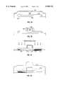
FIGS. 1(A)-1(D) and 2(A)-2(D) are cross-sectional views of a semiconductor device, illustrating a process sequence for fabricating the device by a method according to the present invention;
FIG. 3 is a cross-sectional view of a contact hole formed by the process sequence shown in FIGS. 1(A)-1(D) and 2(A)-2(B);
FIG. 4 is a cross-sectional view of a contact hole as shown in FIG. 2 (C) in which corners have been rounded off by a method according to the present invention;
FIG. 5 is a graph illustrating the endpoint of a dry etching process;
FIGS. 6(A)-6(C), 7(A)-7(B), and 8(A)-8(B) are cross-sectional views illustrating IC fabrication processes according to the invention.
Embodiment 1
A process sequence for fabricating TFTs in accordance with the present invention is illustrated in FIGS. 1(A)-1(D) and FIGS. 2(A)-2(D).
First, aglass substrate 101 having an insulating film such as a silicon oxide film on its surface is prepared. An amorphous silicon film (not shown) having a thickness of 500 Å is formed on the substrate by plasma CVD or LP thermal chemical vapor deposition. The amorphous film is crystallized by an appropriate crystallization method, which may be either heating or laser illumination.
Then, the crystalline silicon film obtained by crystallizing the amorphous silicon film is patterned into islands of asemiconductor layer 102 forming an active layer.
Asilicon oxide film 103 which will act as a gate-insulating film later is formed on the semiconductor layer to a thickness of 1200 Å by plasma CVD or LP thermal chemical vapor deposition.
Then, afilm 104 consisting only or mainly of aluminum is formed to a thickness of 4000 Å. Thisfilm 104 will act as a gate electrode later. Of course, other materials capable of being anodized such as tantalum and niobium may also be used.
Thereafter, anodization is carried out within an electrolytic solution, using thealuminum film 104 as an anode. The electrolytic solution is neutralizing 3% ethylene glycol solution of tartaric acid with aqueous ammonia and adjusting it to a pH of 6.92. Using a platinum cathode, the liquid is processed with an electric current of 5 mA. The voltage is increased up to 10 V.
A denseanodic oxide film 105 formed in this way acts to improve the adhesion to photoresist later. The thickness of theanodic oxide film 105 can be controlled by controlling the voltage application time (FIG. 1(A)).
Then thealuminum film 104 is patterned to formed a gate electrode (not shown).
Then, a second anodic oxidation process is carried out to form a porousanodic oxide film 106. As an electrolytic solution, 3% aqueous solution of oxalic acid is used. A platinum cathode is employed. It is processed with an electric current of 2 to 3 mA. The voltage is increased up to 8 V.
At this time, the anodic oxidation progresses parallel to the substrate. The width of the porousanodic oxide film 106 can be controlled by the voltage application time.
After removing the photoresist with appropriate peeling liquid, a third anodic oxidation process is performed, thus obtaining a state shown in FIG. 1(B).
At this time, the electrolytic solution is neutralizing 3% ethylene glycol solution of tartaric acid with aqueous ammonia and adjusted to a pH of 6.92. Using a platinum cathode, the anodic oxidation is performed with an electric current of 5 to 6 mA. The voltage is increased up to 100 V.
The resultinganodic oxide film 107 is very dense and firm. Therefore, this protects thegate electrode 108 from damage in later steps such as implantation step.
The firmanodic oxide film 107 is not readily etched and so the etching time is prolonged when contact holes are formed. Therefore, it is desired to suppress the thickness of the film below 1000 Å.
Then, a dopant is implanted into the islands ofsemiconductor layer 102 by the ion implantation process. For example, when an N-channel TFT is manufactured, phosphorus (P) may be used as the dopant.
First, under the condition of FIG. 1(B), a first ion implantation process is carried out. Phosphorus (P) is implanted at an accelerating voltage of 60 to 90 kV at a dose of 0.2 to 5×10¹⁵ atoms/cm2. In the present example, the accelerating voltage is 80 kV, and the dose is 1×10¹⁵ atoms/cm2.
Using thegate electrode 108 and the porousanodic oxide film 106 as masks.Regions
Then, as shown in FIG. 1(C), the porousanodic oxide film 106 is removed, and a second implantation process is performed. The second incorporation of phosphorus (P) is carried out at an accelerating voltage of 60 to 90 kV at a dose of 0.1 to 5×10¹⁴ atoms/cm2. In the present example, the accelerating voltage is 80 kV, and the dose is 1×10¹⁴ atoms/cm2.
Thegate electrode 108 serves as a mask.Regions source drain 109 and drainregion 110 are formed by self-aligned technology.
At the same time, aregion 113 acting as a channel for the TFT is formed by self-aligned technology, because no dopant is implanted at all right under thegate electrode 108.
The lightly doped drain (LDD)regions 112 formed in this way suppress generation of a high electric field between thechannel region 113 and thedrain region 110.
Then, irradiating with KrF excimer laser light and thermally annealing are performed. In the present example, the energy density of the laser light is 250 to 300 mJ/cm2. The thermal annealing is carried out at 300 to 450° C. for 1 hour.
This step can heal the damage to the crystallinity of the islands ofsemiconductor layer 102 sustained by the ion implantation process.
Then, as shown in FIG. 1(D), two interlayer insulatingfilms interlayer insulating films
At this time, the composition ratio of the silicon nitride film forming the secondinterlayer insulating film 115 gives a higher dry etch rate than that of the firstinterlayer insulating film 114. For example, the film of higher etch rate can be formed by increasing the pressure of the film-forming gas or the growth temperature or by lowering the RF power.
More specifically, where the first and second films are grown at 250° C. and 350° C., respectively, the dry etch rate of the second layer is approximately twice as high as the rate of the first layer.
The pressures of the gases for forming the first and second layers, respectively, are set to 0.3 and 0.7 torr, respectively. In this case, the dry etch rate of the second layer is about 1.5 times as high as the rate of the first layer.
This is a requirement which must be satisfied in order that the tilt angle β of the secondinterlayer insulating film 115 be smaller than the tilt angle α of the firstinterlayer insulating film 114 in the shape of the contact hole shown in FIG. 3.
The total thickness of the first and second interlayer insulating films is 1 to 3 times as large as the thickness of thegate electrode 108 to improve the coverage of the interlayer insulating films. Thus, current leaking via the interlayer insulating films is prevented.
Preferably, the thickness of the firstinterlayer insulating film 114 is less than one third of the total thickness. If the thickness of the first interlayer insulating film is greater than this, the tilt angle α increases, thus resulting in difficulties in a light etching step carried out later.
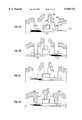
A resist mask indicated by 201 in FIG. 2(A) is formed, and a contact hole is formed by dry etching techniques. The composition of the etchant gas is so set that CF4 :O2 =40:60.
The etching ends when a period of 150 seconds passes since the endpoint has been confirmed. The endpoint is detected as shown in FIG. 5. The signal intensity of nitrogen ions from the first layer is greater, because the first layer is denser than the second layer.
At this time, in the source/drain contact regions film 103 acts as a film that stops the dry etching process. In thegate electrode region 204, theanodic oxide film 107 acts as a film that stops the dry etching process.
Since the secondinterlayer insulating film 115 is higher in etch rate than the firstinterlayer insulating film 114, tapered sections are formed as shown in FIG. 2(A).
Then, the gate-insulatingfilm 103 at the bottom surface of the contact hole is etched with buffered hydrofluoric acid, thus completing the contact holes in the source/drain regions.
Thereafter, chromium mixed acid solution consisting of mixture of chromic acid, acetic acid, phosphoric acid, and nitric acid is used to etch theanodic oxide film 107, thus completing the contact hole in the gate electrode region.
Where the gate-insulatingfilm 103 is etched first in this way, thegate electrode 108 can be protected, since theanodic oxide film 107 has excellent resistance to buffered hydrofluoric acid. The chromium mixed acid solution hardly attacks thesource region 109 or drainregion 110.
In this way, the state shown in FIG. 2(B) is obtained. Wet etching using buffered hydrofluoric acid or chromium mixed acid progresses isotropically and so overetched portions as shown in the circles of FIG. 2(B) are formed.
The interlayer insulating films are recessed by light etching, thus eliminating overetched portions, as shown in FIG. 2(C). At this time, as the tilt angle α of the firstinterlayer insulating film 114 decreases, the film can be more easily recessed.
This light etching process is carried out by dry etching techniques. The composition of the etchant gas is so set that CF4 :O2 =25:75. With this composition, the selectivity of silicon nitride with respect to silicon is more than 10. Hence, the surfaces of thesource region 109 and drainregion 110 are hardly etched.
This light etching is carried out by the gas with a high O2 content. Therefore, the resistmask 201 is recessed simultaneously. Consequently, the corners of the cross-sectional shape at the edges of the contact hole are etched away and rounded off, as shown in the circle of FIG. 4.
After the completion of the contact hole,interconnect electrodes
A thin-film transistor as shown in FIG. 2(D) is fabricated by performing the steps described above.
Embodiment 2
The present example is an example of application of the present invention to an IC fabrication process using single-crystal silicon wafer. More specifically, this is an example of fabrication of a MOS transistor. using the silicon wafer.
The process sequence of the present invention is shown in FIGS. 6(A)-6(C), 7(A)-7(B), and 8(A)-8(B). First, as shown in FIG. 6(A), a thermal oxide film and a silicon nitride film are laminated over an N-type single-crystal silicon wafer 601 and patterned to create a patterned lamination of thethermal oxide film 602 andsilicon nitride film 603.
Then,field oxide films
Then, thethermal oxide film 602 and thesilicon nitride film 603 are removed. Athermal oxide film 606 is formed again by thermal oxidation. Thisthermal oxide film 606 forms a gate-insulating film.
Thereafter, agate electrode 607 is fabricated from an appropriate metal material, silicide material, or semiconductor material. Subsequently, dopants are implanted to form source/drain regions.
In this example, boron (B) ions are introduced through ion implantation to fabricate a P-channel MOS transistor. If an N-channel MOS transistor is fabricated, phosphorus (P) ions may be introduced.
After the ion implantation described above, a heat-treatment is made to activate the introduced dopants and to anneal out damage to the semiconductor layer caused by the ion implantation.
In this way, a P-type source region 608 and adrain region 609 are formed by self-aligned technology, as shown in FIG. 6(B).
Then,silicon nitride films silicon nitride films film 611 has a higher etch rate than thebelow film 610.
A state shown in FIG. 6(C) is obtained in this manner. Then, as shown in FIG. 7(A), a resistmask 612 is placed. Contact holes 613 and 614 are formed by dry etching techniques.
A state shown in FIG. 7(A) is obtained in this way. At this time the gate-insulatingfilm 606 consisting of a thermal oxide film acts as an etch stopper.
Contact holes 615 and 616 are then formed by wet etching techniques.
In this manner, a state shown in FIG. 7(B) is obtained. At this time wet etching proceeds isotropically and so the contact holes 615 and 616 widen the bottoms of the contact holes 613 and 614, respectively.
Then, the interlayer insulating films and resist mask are recessed by light dry etching, using mixture of CF4 and O2. The oxygen is added, because the resist mask should be recessed.
In this way, contacts having a mild cross-sectional shape as shown in FIG. 8(A) can be obtained. After obtaining the state shown in FIG. 8(A), asource electrode 619 and adrain electrode 620 are formed as shown in FIG. 8(B), thus completing a MOS transistor.
In the present invention, the interlayer insulating film is made of a multilayer structure consisting of two or more layers. The etch rate of an upper layer is made higher than that of a lower layer. Therefore, tapered section can be formed in such a way that the tilt angle decreases successively from the top layer of the interlayer insulating film toward the bottom layer.
Furthermore, undercutting of the gate-insulatingfilm 103 and of theanodic oxide film 107 as shown in the circles of FIG. 2(B) can be prevented. In addition, the cross-sectional shape around the top of each contact hole can be improved as shown in FIGS. 2(C) and 3.
The cross-sectional shape of the contact hole can be improved greatly by the effects described above. The yield at which TFTs are fabricated and the reliability of interconnect contacts are enhanced. Concomitantly, the long-term reliability of the devices and display system can be enhanced.
Claims (27)
1. A method for fabricating a semiconductor device comprising the steps of:
forming a semiconductor film on an insulating surface, said semiconductor film having at least channel, source and drain regions therein;
forming a first insulating film on said semiconductor film;
forming a second insulating film on said first insulating film, said second insulating film comprising a different material from said first insulating film;
forming a first opening in said second insulating film by etching to expose a portion of said first insulating film in said first opening;
forming a second opening in said first insulating film in order to expose a portion of said semiconductor film by etching the portion of said first insulating film exposed in said first opening using a liquid etchant whereby a portion of said second insulating film projects over said second opening;
removing the projecting portion of said second insulating film by etching.
2. The method according to claim 1, wherein said first insulating film comprises silicon oxide.
3. The method according to claim 1, wherein said second insulating film comprises a material selected from the group consisting of silicon nitride and organic resin.
4. The method according to claim 1, wherein said second insulating film comprises at least two laminated layers including an upper layer and a lower layer.
5. The method according to claim 4, wherein said first opening has tapered configuration and said upper layer has a higher degree of tapering than said lower layer.
6. The method according to claim 1, wherein said liquid etchant comprises buffered hydrofluoric acid.
7. The method according to claim 1, wherein the etching of said projecting portion is conducted by dry etching with an etching gas comprising carbon tetrafluoride and oxygen.
8. A method for fabricating a semiconductor device comprising the steps of:
forming a semiconductor film on an insulating surface, said semiconductor film having at least channel, source and drain regions therein;
forming a first insulating film on said semiconductor film;
forming an interlayer insulating film over said semiconductor film and said first insulating film, said interlayer insulating film comprising a different material from said first insulating film;
forming a first opening in said interlayer insulating film by etching to expose a portion of said first insulating film in said first opening;
forming a second opening in said first insulating film in order to expose a portion of said semiconductor film by etching the portion of said first insulating film exposed in said first opening using a liquid etchant whereby a portion of said interlayer insulating film projects over said second opening;
removing the projecting portion of said interlayer insulating film by etching.
9. The method according to claim 8, wherein said first insulating film comprises silicon oxide.
10. The method according to claim 8, wherein said interlayer insulating film comprises a material selected from the group consisting of silicon nitride and organic resin.
11. The method according to claim 8, wherein said interlayer insulating film comprises at least two laminated layers including an upper layer and a lower layer.
12. The method according to claim 11, wherein said first opening has a tapered configuration and said upper layer has a higher degree of tapering than said lower layer.
13. The method according to claim 8, wherein said liquid etchant comprises buffered hydrofluoric acid.
14. The method according to claim 8, wherein the etching of said projecting portion is conducted by dry etching with an etching gas comprising carbon tetrafluoride and oxygen.
15. A method for fabricating a semiconductor device comprising the steps of:
forming a semiconductor film on an insulating surface, said semiconductor film having at least channel, source and drain regions therein;
forming a first insulating film on said semiconductor film;
forming a second insulating film on said first insulating film, said second insulating film comprising a different material from said first insulating film;
forming a first opening in said second insulating film by first dry etching using a first etching gas containing oxygen to expose a portion of said first insulating film in said first opening;
forming a second opening in said first insulating film in order to expose a portion of said semiconductor film by etching the portion of said first insulating film exposed in said first opening using a liquid etchant whereby a portion of said second insulating film projects over said second opening;
removing the projecting portion of said second insulating film by second dry etching using a second etching gas containing oxygen, and
wherein a proportion of the oxygen in said second etching gas is higher than a proportion of the oxygen in said first etching gas.
16. The method according to claim 15, wherein said first insulating film comprises silicon oxide.
17. The method according to claim 15, wherein said second insulating film comprises a material selected from the group consisting of silicon nitride and organic resin.
18. The method according to claim 15, wherein said second insulating film comprises at least two laminated layers including an upper layer and a lower layer.
19. The method according to claim 18, wherein said first opening has tapered configuration and said upper layer has a higher degree of tapering than said lower layer.
20. The method according to claim 15, wherein said liquid etchant comprises buffered hydrofluoric acid.
21. The method according to claim 15, wherein each of said first and second etching gas comprises said oxygen and carbon tetrafluoride.
22. A method for fabricating a semiconductor device comprising the steps of:
forming a semiconductor film on an insulating surface, said semiconductor film having at least channel, source and drain regions therein;
forming a first insulating film on said semiconductor film;
forming an interlayer insulating film consisting of a plurality of insulating layers over said semiconductor film and said first insulating film;
first etching said interlayer insulating film to expose a portion of said first insulating film in an opening;
second etching the portion of said first insulating film exposed by said first etching to expose a portion of said semiconductor film in said opening, whereby a portion of said interlayer insulating film projects over said opening; and
removing the projecting portion of said interlayer insulating film by etching,
wherein at least one of said plurality of insulating layers in said interlayer insulating layer comprises organic resin.
23. The method according to claim 22 wherein said first insulating film comprises silicon oxide.
24. The method according to claim 22 wherein another one of said plurality of insulating layers in said interlayer insulating layer comprises silicon nitride.
25. The method according to claim 22 wherein said second etching is performed using said liquid etchant comprising buffered hydrofluoric acid.
26. The method according to claim 22 wherein the removing of said projecting portion is conducted by dry etching with an etching gas comprising carbon tetrafluoride and oxygen.
27. The method according to claim 22 wherein said source and drain regions are doped with phosphorus at a dose of 0.2 to 5×10¹⁵ atoms/cm2, respectively.
Priority Applications (4)
| Application Number | Priority Date | Filing Date | Title |
|---|---|---|---|
| US09/362,808US7786553B1 (en) | 1995-11-27 | 1999-07-28 | Method of fabricating semiconductor device |
| US11/211,694US7800235B2 (en) | 1995-11-27 | 2005-08-26 | Method of fabricating semiconductor device |
| US12/883,526US8283788B2 (en) | 1995-11-27 | 2010-09-16 | Method of fabricating semiconductor device |
| US13/420,646US20120168880A1 (en) | 1995-11-27 | 2012-03-15 | Method of Fabricating Semiconductor Device |
Applications Claiming Priority (2)
| Application Number | Priority Date | Filing Date | Title |
|---|---|---|---|
| JP7-332629 | 1995-11-27 | ||
| JP33262995 | 1995-11-27 |
Related Child Applications (1)
| Application Number | Title | Priority Date | Filing Date |
|---|---|---|---|
| US09/362,808DivisionUS7786553B1 (en) | 1995-11-27 | 1999-07-28 | Method of fabricating semiconductor device |
Publications (1)
| Publication Number | Publication Date |
|---|---|
| US5940732Atrue US5940732A (en) | 1999-08-17 |
Family
ID=18257099
Family Applications (5)
| Application Number | Title | Priority Date | Filing Date |
|---|---|---|---|
| US08/753,428Expired - LifetimeUS5940732A (en) | 1995-11-27 | 1996-11-25 | Method of fabricating semiconductor device |
| US09/362,808Expired - Fee RelatedUS7786553B1 (en) | 1995-11-27 | 1999-07-28 | Method of fabricating semiconductor device |
| US11/211,694Expired - Fee RelatedUS7800235B2 (en) | 1995-11-27 | 2005-08-26 | Method of fabricating semiconductor device |
| US12/883,526Expired - Fee RelatedUS8283788B2 (en) | 1995-11-27 | 2010-09-16 | Method of fabricating semiconductor device |
| US13/420,646AbandonedUS20120168880A1 (en) | 1995-11-27 | 2012-03-15 | Method of Fabricating Semiconductor Device |
Family Applications After (4)
| Application Number | Title | Priority Date | Filing Date |
|---|---|---|---|
| US09/362,808Expired - Fee RelatedUS7786553B1 (en) | 1995-11-27 | 1999-07-28 | Method of fabricating semiconductor device |
| US11/211,694Expired - Fee RelatedUS7800235B2 (en) | 1995-11-27 | 2005-08-26 | Method of fabricating semiconductor device |
| US12/883,526Expired - Fee RelatedUS8283788B2 (en) | 1995-11-27 | 2010-09-16 | Method of fabricating semiconductor device |
| US13/420,646AbandonedUS20120168880A1 (en) | 1995-11-27 | 2012-03-15 | Method of Fabricating Semiconductor Device |
Country Status (3)
| Country | Link |
|---|---|
| US (5) | US5940732A (en) |
| JP (9) | JP2008147692A (en) |
| KR (2) | KR100318838B1 (en) |
Cited By (53)
| Publication number | Priority date | Publication date | Assignee | Title |
|---|---|---|---|---|
| US6163067A (en)* | 1995-09-29 | 2000-12-19 | Kabushiki Kaisha Toshiba | Semiconductor apparatus having wiring groove and contact hole in self-alignment manner |
| US6180997B1 (en)* | 1998-02-23 | 2001-01-30 | Winbond Electronics Corp. | Structure for a multi-layered dielectric layer and manufacturing method thereof |
| US6225152B1 (en) | 1996-01-20 | 2001-05-01 | Semiconductor Energy Laboratory Co., Ltd. | Semiconductor device and fabrication method thereof |
| US6294799B1 (en) | 1995-11-27 | 2001-09-25 | Semiconductor Energy Laboratory Co., Ltd. | Semiconductor device and method of fabricating same |
| US6316810B1 (en)* | 1996-01-19 | 2001-11-13 | Semiconductor Energy Laboratory Co., Ltd. | Display switch with double layered gate insulation and resinous interlayer dielectric |
| US20020055206A1 (en)* | 1995-01-17 | 2002-05-09 | Hongyong Zhang | Method for producing a semiconductor integrated circuit including a thin film transistor and a capacitor |
| US6420777B2 (en)* | 1998-02-26 | 2002-07-16 | International Business Machines Corporation | Dual layer etch stop barrier |
| US20020118318A1 (en)* | 2001-02-23 | 2002-08-29 | Nec Corporation | Liquid crystal display device and its manufacturing method |
| US6465287B1 (en) | 1996-01-27 | 2002-10-15 | Semiconductor Energy Laboratory Co., Ltd. | Method for fabricating a semiconductor device using a metal catalyst and high temperature crystallization |
| US6475837B2 (en)* | 1996-06-25 | 2002-11-05 | Semiconductor Energy Laboratory Co., Ltd. | Electro-optical device |
| US6478263B1 (en) | 1997-01-17 | 2002-11-12 | Semiconductor Energy Laboratory Co., Ltd. | Semiconductor device and its manufacturing method |
| US6504174B1 (en) | 1996-01-19 | 2003-01-07 | Semiconductor Energy Laboratory Co., Ltd. | Semiconductor device and method for fabricating the same |
| US6518596B1 (en)* | 1999-11-04 | 2003-02-11 | Pacific Solar Pty Ltd. | Formation of contacts on thin films |
| US6528820B1 (en) | 1996-01-19 | 2003-03-04 | Semiconductor Energy Laboratory Co., Ltd. | Semiconductor device and method of fabricating same |
| US20030193054A1 (en)* | 2002-04-15 | 2003-10-16 | Semiconductor Energy Laboratory Co., Ltd. | Display device and method of fabricating the same |
| US6744069B1 (en) | 1996-01-19 | 2004-06-01 | Semiconductor Energy Laboratory Co., Ltd. | Semiconductor device and its manufacturing method |
| US20040140471A1 (en)* | 1999-03-29 | 2004-07-22 | Semiconductor Energy Laboratory Co., Ltd. | Semiconductor device and manufacturing method thereof |
| US20050040531A1 (en)* | 2003-08-05 | 2005-02-24 | Semiconductor Energy Laboratory Co., Ltd. | Wiring board, manufacturing method thereof, semiconductor device and manufacturing method thereof |
| US20050056849A1 (en)* | 1996-03-21 | 2005-03-17 | Semiconductor Energy Laboratory Co., Ltd., A Japan Corporation | Semiconductor device and method of making thereof |
| US20050059192A1 (en)* | 2003-09-17 | 2005-03-17 | Hui-Chu Lin | Method of fabricating low temperature polysilicon thin film transistor |
| US20050059191A1 (en)* | 2003-09-17 | 2005-03-17 | Hui-Chu Lin | Method of fabricating low temperature polysilicon thin film transistor |
| US7019385B1 (en) | 1996-04-12 | 2006-03-28 | Semiconductor Energy Laboratory Co., Ltd. | Semiconductor device and method of fabricating same |
| US7037811B1 (en) | 1996-01-26 | 2006-05-02 | Semiconductor Energy Laboratory Co., Ltd. | Method for fabricating a semiconductor device |
| US7056381B1 (en) | 1996-01-26 | 2006-06-06 | Semiconductor Energy Laboratory Co., Ltd. | Fabrication method of semiconductor device |
| US7135741B1 (en) | 1996-03-17 | 2006-11-14 | Semiconductor Energy Laboratory Co., Ltd. | Method of manufacturing a semiconductor device |
| US20080057604A1 (en)* | 2006-08-29 | 2008-03-06 | Semiconductor Energy Laboratory Co., Ltd. | Method of fabricating display device |
| US20080237876A1 (en)* | 2007-03-26 | 2008-10-02 | Semiconductor Energy Laboratory Co., Ltd. | Semiconductor device and method for manufacturing the same |
| US20080237875A1 (en)* | 2007-03-26 | 2008-10-02 | Semiconductor Energy Laboratory Co., Ltd. | Semiconductor device and method for manufacturing the same |
| US20090017576A1 (en)* | 2007-07-09 | 2009-01-15 | Swarnal Borthakur | Semiconductor Processing Methods |
| US20090212295A1 (en)* | 2004-05-24 | 2009-08-27 | Samsung Mobile Display Co., Ltd. | Semiconductor device and method of fabricating the same |
| US20090242894A1 (en)* | 2008-03-26 | 2009-10-01 | Au Optronics Corp. | Thin-Film-Transistor Structure, Pixel Structure and Manufacturing Method Thereof |
| US20090250701A1 (en)* | 2005-08-11 | 2009-10-08 | Tomohiro Kimura | Circuit board, electronic device, and method for producing circuit board |
| US7671369B2 (en) | 2002-04-09 | 2010-03-02 | Semiconductor Energy Laboratory Co., Ltd. | Semiconductor display device |
| US7709837B2 (en) | 1996-01-19 | 2010-05-04 | Semiconductor Energy Laboratory Co., Ltd | Semiconductor device and its manufacturing method |
| US7786553B1 (en) | 1995-11-27 | 2010-08-31 | Semiconductor Energy Laboratory Co., Ltd. | Method of fabricating semiconductor device |
| US20100301486A1 (en)* | 2009-05-29 | 2010-12-02 | Kai Frohberg | High-aspect ratio contact element with superior shape in a semiconductor device for improving liner deposition |
| US7955975B2 (en) | 2002-04-09 | 2011-06-07 | Semiconductor Energy Laboratory Co., Ltd. | Semiconductor element and display device using the same |
| US7964874B2 (en) | 2002-04-15 | 2011-06-21 | Semiconductor Energy Laboratory Co., Ltd. | Semiconductor device having a protective circuit |
| US8120031B2 (en) | 2002-05-17 | 2012-02-21 | Semiconductor Energy Laboratory Co., Ltd. | Display device including an opening formed in a gate insulating film, a passivation film, and a barrier film |
| DE102010064289A1 (en)* | 2010-12-28 | 2012-06-28 | GLOBALFOUNDRIES Dresden Module One Ltd. Liability Company & Co. KG | Size reduction of contact elements and vias in a semiconductor device by incorporation of an additional chamfer material |
| CN105334680A (en)* | 2014-08-15 | 2016-02-17 | 群创光电股份有限公司 | Array substrate structure and contact structure |
| US20160049479A1 (en)* | 2014-08-15 | 2016-02-18 | Innolux Corporation | Array substrate structure and contact structure |
| US9349673B2 (en) | 2012-07-04 | 2016-05-24 | Seiko Epson Corporation | Substrate, method of manufacturing substrate, semiconductor device, and electronic apparatus |
| US9564474B2 (en) | 2012-06-21 | 2017-02-07 | Joled Inc. | TFT substrate, method for producing same, organic EL display device, and method for manufacturing organic EL display device |
| US20170194229A1 (en)* | 2015-12-30 | 2017-07-06 | Globalfoundries Singapore Pte. Ltd. | Integrated circuits with aluminum via structures and methods for fabricating the same |
| US9818849B2 (en) | 2011-06-17 | 2017-11-14 | Semiconductor Energy Laboratory Co., Ltd. | Manufacturing method of semiconductor device with conductive film in opening through multiple insulating films |
| US10276378B1 (en)* | 2017-10-30 | 2019-04-30 | Taiwan Semiconductor Manufacturing Co., Ltd. | Method of forming funnel-like opening for semiconductor device structure |
| US20190165119A1 (en)* | 2017-11-28 | 2019-05-30 | Panasonic Intellectual Property Management Co., Ltd. | Semiconductor device and method for manufacturing same |
| US10629622B2 (en) | 2017-08-31 | 2020-04-21 | Japan Display Inc. | Display device and manufacturing method thereof |
| US10707240B2 (en) | 2017-09-07 | 2020-07-07 | Japan Display Inc. | Display device |
| US11133337B2 (en) | 2017-10-26 | 2021-09-28 | Japan Display Inc. | Display device and method for manufacturing same |
| US11362113B2 (en)* | 2019-08-26 | 2022-06-14 | Japan Display Inc. | Semiconductor device and method of manufacturing semiconductor device |
| US12348006B2 (en) | 2020-03-16 | 2025-07-01 | Mitsubishi Electric Corporation | Semiconductor device and method for manufacturing semiconductor device |
Families Citing this family (24)
| Publication number | Priority date | Publication date | Assignee | Title |
|---|---|---|---|---|
| KR100778834B1 (en)* | 2000-02-21 | 2007-11-22 | 엘지.필립스 엘시디 주식회사 | Method of manufacturing thin film transistor and method of manufacturing liquid crystal display device using same |
| US7785938B2 (en)* | 2006-04-28 | 2010-08-31 | Semiconductor Energy Laboratory Co., Ltd | Semiconductor integrated circuit, manufacturing method thereof, and semiconductor device using semiconductor integrated circuit |
| US7947606B2 (en)* | 2008-05-29 | 2011-05-24 | Infineon Technologies Ag | Methods of forming conductive features and structures thereof |
| JP4752967B2 (en) | 2009-01-27 | 2011-08-17 | カシオ計算機株式会社 | Multilayer film forming method and display panel manufacturing method |
| KR101057192B1 (en)* | 2009-04-30 | 2011-08-16 | 주식회사 하이닉스반도체 | How to form a pattern on a wafer by exposure process |
| JP2012038965A (en)* | 2010-08-09 | 2012-02-23 | Lapis Semiconductor Co Ltd | Semiconductor device and manufacturing method of the same |
| KR101506303B1 (en) | 2011-09-29 | 2015-03-26 | 가부시키가이샤 한도오따이 에네루기 켄큐쇼 | Semiconductor device and method for manufacturing the same |
| CN103050433A (en)* | 2011-10-17 | 2013-04-17 | 中芯国际集成电路制造(上海)有限公司 | Semiconductor contact hole structure and manufacturing method thereof |
| US9847225B2 (en)* | 2011-11-15 | 2017-12-19 | Taiwan Semiconductor Manufacturing Company, Ltd. | Semiconductor device and method of manufacturing the same |
| KR102014169B1 (en)* | 2012-07-30 | 2019-08-27 | 삼성디스플레이 주식회사 | Organic light emitting display apparatus and method of manufacturing the same |
| KR102091444B1 (en) | 2013-10-08 | 2020-03-23 | 삼성디스플레이 주식회사 | Display substrate and method of manufacturing a display substrate |
| US20150263026A1 (en)* | 2014-03-12 | 2015-09-17 | Kabushiki Kaisha Toshiba | Semiconductor device and design apparatus for semiconductor device |
| CN104218094B (en)* | 2014-08-28 | 2016-11-23 | 京东方科技集团股份有限公司 | A kind of thin film transistor (TFT), display base plate and display device |
| MY185098A (en)* | 2014-08-29 | 2021-04-30 | Mimos Berhad | A method for manufacturing a large schottky diode |
| CN104701255B (en)* | 2015-03-18 | 2017-12-29 | 信利(惠州)智能显示有限公司 | The preparation method of low substrate of LCD device |
| CN104882485A (en)* | 2015-03-30 | 2015-09-02 | 深超光电(深圳)有限公司 | Thin film transistor and manufacturing method thereof |
| CN106449654B (en)* | 2016-10-14 | 2019-12-31 | 京东方科技集团股份有限公司 | A kind of substrate and its preparation method, display device |
| CN109755260A (en) | 2018-12-24 | 2019-05-14 | 惠科股份有限公司 | Display panel, manufacturing method of display panel and display device |
| CN210110300U (en)* | 2019-08-16 | 2020-02-21 | 北京京东方技术开发有限公司 | Pixel drive circuit, array substrate and display device |
| CN110517986B (en)* | 2019-09-17 | 2021-10-08 | 合肥领盛电子有限公司 | A kind of manufacturing method of TFT backplane |
| US11521846B2 (en) | 2019-12-16 | 2022-12-06 | Taiwan Semiconductor Manufacturing Company Limited | Methods for patterning a silicon oxide-silicon nitride-silicon oxide stack and structures formed by the same |
| CN111524957B (en)* | 2020-05-09 | 2024-02-23 | 京东方科技集团股份有限公司 | Display substrate, manufacturing method thereof and display device |
| CN111584526B (en)* | 2020-05-28 | 2022-06-24 | 京东方科技集团股份有限公司 | Display substrate, manufacturing method thereof, and display device |
| CN111725324B (en) | 2020-06-11 | 2021-11-02 | 武汉华星光电半导体显示技术有限公司 | Thin film transistor, array substrate and manufacturing method thereof |
Citations (11)
| Publication number | Priority date | Publication date | Assignee | Title |
|---|---|---|---|---|
| NL7314375A (en)* | 1972-10-18 | 1974-04-22 | ||
| US4342617A (en)* | 1981-02-23 | 1982-08-03 | Intel Corporation | Process for forming opening having tapered sides in a plasma nitride layer |
| US4495220A (en)* | 1983-10-07 | 1985-01-22 | Trw Inc. | Polyimide inter-metal dielectric process |
| US4814041A (en)* | 1986-10-08 | 1989-03-21 | International Business Machines Corporation | Method of forming a via-hole having a desired slope in a photoresist masked composite insulating layer |
| US5117278A (en)* | 1989-04-20 | 1992-05-26 | U.S. Philips Corporation | Semiconductor device having a semiconductor body embedded in an envelope made of synthetic material |
| US5264731A (en)* | 1987-06-25 | 1993-11-23 | Matsushita Electric Industrial Co., Ltd. | Method for fabricating semiconductor device |
| US5414442A (en)* | 1991-06-14 | 1995-05-09 | Semiconductor Energy Laboratory Co., Ltd. | Electro-optical device and method of driving the same |
| US5550405A (en)* | 1994-12-21 | 1996-08-27 | Advanced Micro Devices, Incorporated | Processing techniques for achieving production-worthy, low dielectric, low interconnect resistance and high performance ICS |
| US5604380A (en)* | 1993-10-07 | 1997-02-18 | Mitsubishi Denki Kabushiki Kaisha | Semiconductor device having a multilayer interconnection structure |
| US5620905A (en)* | 1993-10-20 | 1997-04-15 | Semiconductor Energy Laboratory Co., Ltd. | Method of fabricating thin film semiconductor integrated circuit |
| US5719065A (en)* | 1993-10-01 | 1998-02-17 | Semiconductor Energy Laboratory Co., Ltd. | Method for manufacturing semiconductor device with removable spacers |
Family Cites Families (101)
| Publication number | Priority date | Publication date | Assignee | Title |
|---|---|---|---|---|
| JPS5421073B2 (en) | 1974-04-15 | 1979-07-27 | ||
| US4103297A (en) | 1976-12-20 | 1978-07-25 | Hughes Aircraft Company | Light-insensitive matrix addressed liquid crystal display system |
| JPS5519850A (en) | 1978-07-31 | 1980-02-12 | Hitachi Ltd | Semiconductor |
| US4342618A (en)* | 1979-05-14 | 1982-08-03 | Alkibiadis Karnis | Method and apparatus on-line monitoring of fibre length of mechanical pumps |
| JPS55163860A (en) | 1979-06-06 | 1980-12-20 | Toshiba Corp | Manufacture of semiconductor device |
| US4371423A (en) | 1979-09-04 | 1983-02-01 | Vlsi Technology Research Association | Method of manufacturing semiconductor device utilizing a lift-off technique |
| JPS57126147A (en)* | 1981-01-28 | 1982-08-05 | Fujitsu Ltd | Manufacture of semiconductor device |
| JPS592352A (en)* | 1982-06-28 | 1984-01-07 | Toshiba Corp | Manufacturing method of semiconductor device |
| US4461672A (en) | 1982-11-18 | 1984-07-24 | Texas Instruments, Inc. | Process for etching tapered vias in silicon dioxide |
| JPS6313347A (en)* | 1986-07-03 | 1988-01-20 | Matsushita Electric Ind Co Ltd | Manufacture of thin-film semiconductor device |
| JPH0727966B2 (en) | 1986-07-04 | 1995-03-29 | 日立化成工業株式会社 | Semiconductor device |
| JPS6334928A (en) | 1986-07-29 | 1988-02-15 | Mitsubishi Electric Corp | How to form through holes |
| DE3774036D1 (en)* | 1986-08-11 | 1991-11-28 | Siemens Ag | METHOD FOR STABILIZING PN TRANSITIONS. |
| JPS6362352A (en)* | 1986-09-03 | 1988-03-18 | Matsushita Electronics Corp | Manufacture of semiconductor device |
| JPS6396922A (en)* | 1986-10-13 | 1988-04-27 | Matsushita Electric Ind Co Ltd | Manufacture of semiconductor device |
| JPS63131542A (en)* | 1986-11-20 | 1988-06-03 | Nec Kansai Ltd | Manufacture of semiconductor device |
| JPS63276246A (en)* | 1987-05-08 | 1988-11-14 | Nec Corp | Semiconductor device |
| JPS63296353A (en) | 1987-05-28 | 1988-12-02 | Matsushita Electric Ind Co Ltd | Contact hole forming method |
| JPS6433971U (en) | 1987-08-25 | 1989-03-02 | ||
| US5327001A (en) | 1987-09-09 | 1994-07-05 | Casio Computer Co., Ltd. | Thin film transistor array having single light shield layer over transistors and gate and drain lines |
| US5032883A (en) | 1987-09-09 | 1991-07-16 | Casio Computer Co., Ltd. | Thin film transistor and method of manufacturing the same |
| JPH0654774B2 (en) | 1987-11-30 | 1994-07-20 | 株式会社東芝 | Semiconductor device and manufacturing method thereof |
| JP2628339B2 (en) | 1988-05-13 | 1997-07-09 | 日本電信電話株式会社 | Method for manufacturing semiconductor device |
| US4948743A (en)* | 1988-06-29 | 1990-08-14 | Matsushita Electronics Corporation | Method of manufacturing a semiconductor device |
| JPH0225024A (en) | 1988-07-13 | 1990-01-26 | Mitsubishi Electric Corp | Manufacture of semiconductor device |
| JPH0244769A (en) | 1988-08-05 | 1990-02-14 | Hitachi Ltd | Thin film transistor |
| JPH02111054A (en)* | 1988-10-20 | 1990-04-24 | Nec Corp | Semiconductor device and manufacture thereof |
| CA1313563C (en) | 1988-10-26 | 1993-02-09 | Makoto Sasaki | Thin film transistor panel |
| JPH0372623A (en)* | 1989-04-05 | 1991-03-27 | Olympus Optical Co Ltd | Semiconductor device and its manufacture |
| JPH02278749A (en) | 1989-04-20 | 1990-11-15 | Matsushita Electron Corp | Image display device and its manufacture |
| JPH034526A (en)* | 1989-05-31 | 1991-01-10 | Sharp Corp | Manufacture of semiconductor device |
| US5264077A (en) | 1989-06-15 | 1993-11-23 | Semiconductor Energy Laboratory Co., Ltd. | Method for producing a conductive oxide pattern |
| JPH0383341A (en)* | 1989-08-28 | 1991-04-09 | Matsushita Electron Corp | Manufacture of semiconductor device |
| JPH03181134A (en)* | 1989-12-11 | 1991-08-07 | Sharp Corp | How to form multilayer wiring |
| JPH03190232A (en) | 1989-12-20 | 1991-08-20 | Fujitsu Ltd | Manufacturing method of semiconductor device |
| JPH03262133A (en)* | 1990-03-13 | 1991-11-21 | Fujitsu Ltd | Manufacture of semiconductor device |
| JPH03286524A (en) | 1990-04-03 | 1991-12-17 | Kawasaki Steel Corp | Manufacture of semiconductor device |
| JPH0821582B2 (en) | 1990-04-25 | 1996-03-04 | 三洋電機株式会社 | Semiconductor integrated circuit and manufacturing method thereof |
| US5056895A (en) | 1990-05-21 | 1991-10-15 | Greyhawk Systems, Inc. | Active matrix liquid crystal liquid crystal light valve including a dielectric mirror upon a leveling layer and having fringing fields |
| JPH0476915A (en)* | 1990-07-19 | 1992-03-11 | Oki Electric Ind Co Ltd | Manufacture of semiconductor device |
| US5182624A (en) | 1990-08-08 | 1993-01-26 | Minnesota Mining And Manufacturing Company | Solid state electromagnetic radiation detector fet array |
| JPH04142740A (en)* | 1990-10-03 | 1992-05-15 | Oki Electric Ind Co Ltd | Formation of contact hole |
| JP2699644B2 (en)* | 1990-10-30 | 1998-01-19 | 日本電気株式会社 | Method for manufacturing semiconductor device |
| KR950013784B1 (en) | 1990-11-20 | 1995-11-16 | 가부시키가이샤 한도오따이 에네루기 겐큐쇼 | Field effect trasistor and its making method and tft |
| US5849601A (en) | 1990-12-25 | 1998-12-15 | Semiconductor Energy Laboratory Co., Ltd. | Electro-optical device and method for manufacturing the same |
| KR950001360B1 (en) | 1990-11-26 | 1995-02-17 | 가부시키가이샤 한도오따이 에네루기 겐큐쇼 | Electro-optical device and its driving method |
| JPH04251926A (en)* | 1991-01-10 | 1992-09-08 | Fujitsu Ltd | Manufacture of semiconductor device |
| JPH06104281A (en)* | 1991-02-06 | 1994-04-15 | Seiko Epson Corp | Thin film transistor and manufacturing method thereof |
| JPH04257270A (en)* | 1991-02-08 | 1992-09-11 | Fujitsu Ltd | semiconductor storage device |
| EP0499979A3 (en) | 1991-02-16 | 1993-06-09 | Semiconductor Energy Laboratory Co., Ltd. | Electro-optical device |
| JP2794678B2 (en) | 1991-08-26 | 1998-09-10 | 株式会社 半導体エネルギー研究所 | Insulated gate semiconductor device and method of manufacturing the same |
| JP2794499B2 (en) | 1991-03-26 | 1998-09-03 | 株式会社半導体エネルギー研究所 | Method for manufacturing semiconductor device |
| JPH04324629A (en)* | 1991-04-24 | 1992-11-13 | Yamaha Corp | Working method of silicate glass film |
| US5155053A (en) | 1991-05-28 | 1992-10-13 | Hughes Aircraft Company | Method of forming t-gate structure on microelectronic device substrate |
| KR950012918B1 (en) | 1991-10-21 | 1995-10-23 | 현대전자산업주식회사 | Contact filling method using secondary deposition of selective tungsten thin film |
| US5485019A (en) | 1992-02-05 | 1996-01-16 | Semiconductor Energy Laboratory Co., Ltd. | Semiconductor device and method for forming the same |
| US5246883A (en)* | 1992-02-06 | 1993-09-21 | Sgs-Thomson Microelectronics, Inc. | Semiconductor contact via structure and method |
| JP3127580B2 (en)* | 1992-06-03 | 2001-01-29 | カシオ計算機株式会社 | Method for manufacturing thin film transistor |
| JPH06177155A (en)* | 1992-12-08 | 1994-06-24 | Sony Corp | Formation of semiconductor thin film and fabrication of mos transistor |
| DE69332142T2 (en) | 1992-12-25 | 2003-03-06 | Sony Corp., Tokio/Tokyo | Active matrix substrate |
| JPH06268073A (en)* | 1993-01-15 | 1994-09-22 | Sony Corp | Manufacture of semiconductor device |
| JP2789293B2 (en)* | 1993-07-14 | 1998-08-20 | 株式会社半導体エネルギー研究所 | Semiconductor device manufacturing method |
| TW369686B (en) | 1993-07-27 | 1999-09-11 | Semiconductor Energy Lab Corp | Semiconductor device and process for fabricating the same |
| US5492843A (en) | 1993-07-31 | 1996-02-20 | Semiconductor Energy Laboratory Co., Ltd. | Method of fabricating semiconductor device and method of processing substrate |
| US5320981A (en) | 1993-08-10 | 1994-06-14 | Micron Semiconductor, Inc. | High accuracy via formation for semiconductor devices |
| KR100333153B1 (en) | 1993-09-07 | 2002-12-05 | 가부시키가이샤 한도오따이 에네루기 켄큐쇼 | Process for fabricating semiconductor device |
| JP3411408B2 (en)* | 1993-09-07 | 2003-06-03 | 株式会社半導体エネルギー研究所 | Method for manufacturing semiconductor device |
| JPH07161816A (en)* | 1993-12-07 | 1995-06-23 | Sony Corp | Semiconductor device |
| US6475903B1 (en) | 1993-12-28 | 2002-11-05 | Intel Corporation | Copper reflow process |
| JP2991919B2 (en)* | 1994-03-04 | 1999-12-20 | 松下電器産業株式会社 | Method for manufacturing thin film transistor |
| KR100321541B1 (en)* | 1994-03-09 | 2002-06-20 | 야마자끼 순페이 | How Active Matrix Display Devices Work |
| US5621556A (en) | 1994-04-28 | 1997-04-15 | Xerox Corporation | Method of manufacturing active matrix LCD using five masks |
| JPH07302912A (en) | 1994-04-29 | 1995-11-14 | Semiconductor Energy Lab Co Ltd | Semiconductor device |
| JP3072000B2 (en) | 1994-06-23 | 2000-07-31 | 株式会社半導体エネルギー研究所 | Method for manufacturing semiconductor device |
| JP3059915B2 (en) | 1994-09-29 | 2000-07-04 | 三洋電機株式会社 | Display device and method of manufacturing display device |
| US5453403A (en) | 1994-10-24 | 1995-09-26 | Chartered Semiconductor Manufacturing Pte, Ltd. | Method of beveled contact opening formation |
| US6140705A (en)* | 1995-01-03 | 2000-10-31 | Texas Instruments Incorporated | Self-aligned contact through a conducting layer |
| US5602905A (en)* | 1995-01-23 | 1997-02-11 | Mettke; Richard P. | On-line communication terminal/apparatus |
| JPH08250743A (en) | 1995-03-07 | 1996-09-27 | Semiconductor Energy Lab Co Ltd | Method for manufacturing semiconductor device |
| JP3176527B2 (en)* | 1995-03-30 | 2001-06-18 | シャープ株式会社 | Method for manufacturing semiconductor device |
| JP3295679B2 (en) | 1995-08-04 | 2002-06-24 | 株式会社半導体エネルギー研究所 | Method for manufacturing semiconductor device |
| KR970011972A (en) | 1995-08-11 | 1997-03-29 | 쯔지 하루오 | Transmission type liquid crystal display device and manufacturing method thereof |
| US5753952A (en) | 1995-09-22 | 1998-05-19 | Texas Instruments Incorporated | Nonvolatile memory cell with P-N junction formed in polysilicon floating gate |
| JP3299869B2 (en) | 1995-09-27 | 2002-07-08 | シャープ株式会社 | Liquid crystal display device and manufacturing method thereof |
| JP3272212B2 (en) | 1995-09-29 | 2002-04-08 | シャープ株式会社 | Transmissive liquid crystal display device and method of manufacturing the same |
| TW371776B (en) | 1995-10-15 | 1999-10-11 | Semiconductor Energy Lab Co Ltd | Laser irradiation apparatus and method |
| US5552343A (en) | 1995-10-19 | 1996-09-03 | Taiwan Semiconductor Manufacturing Company | Method for tapered contact formation |
| US6027960A (en) | 1995-10-25 | 2000-02-22 | Semiconductor Energy Laboratory Co., Ltd. | Laser annealing method and laser annealing device |
| JP3209317B2 (en) | 1995-10-31 | 2001-09-17 | シャープ株式会社 | Transmissive liquid crystal display device and method of manufacturing the same |
| US6015724A (en) | 1995-11-02 | 2000-01-18 | Semiconductor Energy Laboratory Co. | Manufacturing method of a semiconductor device |
| TW329500B (en) | 1995-11-14 | 1998-04-11 | Handotai Energy Kenkyusho Kk | Electro-optical device |
| TWI228625B (en) | 1995-11-17 | 2005-03-01 | Semiconductor Energy Lab | Display device |
| US5847410A (en) | 1995-11-24 | 1998-12-08 | Semiconductor Energy Laboratory Co. | Semiconductor electro-optical device |
| US5940732A (en) | 1995-11-27 | 1999-08-17 | Semiconductor Energy Laboratory Co., | Method of fabricating semiconductor device |
| US6294799B1 (en) | 1995-11-27 | 2001-09-25 | Semiconductor Energy Laboratory Co., Ltd. | Semiconductor device and method of fabricating same |
| JP3842852B2 (en)* | 1995-11-27 | 2006-11-08 | 株式会社半導体エネルギー研究所 | Method for manufacturing semiconductor device |
| US6927826B2 (en) | 1997-03-26 | 2005-08-09 | Semiconductor Energy Labaratory Co., Ltd. | Display device |
| US5989966A (en) | 1997-12-15 | 1999-11-23 | Taiwan Semiconductor Manufacturing Company, Ltd. | Method and a deep sub-micron field effect transistor structure for suppressing short channel effects |
| US6475836B1 (en) | 1999-03-29 | 2002-11-05 | Semiconductor Energy Laboratory Co., Ltd. | Semiconductor device and manufacturing method thereof |
| JP4037117B2 (en) | 2001-02-06 | 2008-01-23 | 株式会社日立製作所 | Display device |
| TW554199B (en)* | 2001-08-29 | 2003-09-21 | Au Optronics Corp | Reflective thin-film transistor liquid crystal display with rough diffuser |
- 1996
- 1996-11-25USUS08/753,428patent/US5940732A/ennot_activeExpired - Lifetime
- 1996-11-26KRKR1019960057524Apatent/KR100318838B1/ennot_activeExpired - Lifetime
- 1999
- 1999-07-28USUS09/362,808patent/US7786553B1/ennot_activeExpired - Fee Related
- 2001
- 2001-05-16KRKR1020010026635Apatent/KR100339644B1/ennot_activeExpired - Lifetime
- 2005
- 2005-08-26USUS11/211,694patent/US7800235B2/ennot_activeExpired - Fee Related
- 2008
- 2008-01-18JPJP2008009259Apatent/JP2008147692A/ennot_activeWithdrawn
- 2010
- 2010-07-14JPJP2010159513Apatent/JP5025767B2/ennot_activeExpired - Fee Related
- 2010-09-16USUS12/883,526patent/US8283788B2/ennot_activeExpired - Fee Related
- 2011
- 2011-07-14JPJP2011155390Apatent/JP2011238956A/ennot_activeWithdrawn
- 2012
- 2012-01-25JPJP2012012568Apatent/JP5542263B2/ennot_activeExpired - Lifetime
- 2012-03-15USUS13/420,646patent/US20120168880A1/ennot_activeAbandoned
- 2012-05-23JPJP2012117609Apatent/JP2012186498A/ennot_activeWithdrawn
- 2013
- 2013-12-13JPJP2013258316Apatent/JP2014082512A/ennot_activeWithdrawn
- 2014
- 2014-04-03JPJP2014077210Apatent/JP5716110B2/ennot_activeExpired - Lifetime
- 2014-06-27JPJP2014132620Apatent/JP5777777B2/ennot_activeExpired - Lifetime
- 2015
- 2015-05-28JPJP2015108960Apatent/JP6009040B2/ennot_activeExpired - Lifetime
Patent Citations (11)
| Publication number | Priority date | Publication date | Assignee | Title |
|---|---|---|---|---|
| NL7314375A (en)* | 1972-10-18 | 1974-04-22 | ||
| US4342617A (en)* | 1981-02-23 | 1982-08-03 | Intel Corporation | Process for forming opening having tapered sides in a plasma nitride layer |
| US4495220A (en)* | 1983-10-07 | 1985-01-22 | Trw Inc. | Polyimide inter-metal dielectric process |
| US4814041A (en)* | 1986-10-08 | 1989-03-21 | International Business Machines Corporation | Method of forming a via-hole having a desired slope in a photoresist masked composite insulating layer |
| US5264731A (en)* | 1987-06-25 | 1993-11-23 | Matsushita Electric Industrial Co., Ltd. | Method for fabricating semiconductor device |
| US5117278A (en)* | 1989-04-20 | 1992-05-26 | U.S. Philips Corporation | Semiconductor device having a semiconductor body embedded in an envelope made of synthetic material |
| US5414442A (en)* | 1991-06-14 | 1995-05-09 | Semiconductor Energy Laboratory Co., Ltd. | Electro-optical device and method of driving the same |
| US5719065A (en)* | 1993-10-01 | 1998-02-17 | Semiconductor Energy Laboratory Co., Ltd. | Method for manufacturing semiconductor device with removable spacers |
| US5604380A (en)* | 1993-10-07 | 1997-02-18 | Mitsubishi Denki Kabushiki Kaisha | Semiconductor device having a multilayer interconnection structure |
| US5620905A (en)* | 1993-10-20 | 1997-04-15 | Semiconductor Energy Laboratory Co., Ltd. | Method of fabricating thin film semiconductor integrated circuit |
| US5550405A (en)* | 1994-12-21 | 1996-08-27 | Advanced Micro Devices, Incorporated | Processing techniques for achieving production-worthy, low dielectric, low interconnect resistance and high performance ICS |
Cited By (142)
| Publication number | Priority date | Publication date | Assignee | Title |
|---|---|---|---|---|
| US20020055206A1 (en)* | 1995-01-17 | 2002-05-09 | Hongyong Zhang | Method for producing a semiconductor integrated circuit including a thin film transistor and a capacitor |
| US7517738B2 (en) | 1995-01-17 | 2009-04-14 | Semiconductor Energy Laboratory Co., Ltd. | Method for producing a semiconductor integrated circuit including a thin film transistor and a capacitor |
| US20080246039A1 (en)* | 1995-01-17 | 2008-10-09 | Semiconductor Energy Laboratory Co., Ltd. | Method for producing a semiconductor integrated circuit including a thin film transistor and a capacitor |
| US7687809B2 (en) | 1995-01-17 | 2010-03-30 | Semiconductor Energy Laboratory Co., Ltd | Method for producing a semiconductor integrated circuit including a thin film transistor and a capacitor |
| US6163067A (en)* | 1995-09-29 | 2000-12-19 | Kabushiki Kaisha Toshiba | Semiconductor apparatus having wiring groove and contact hole in self-alignment manner |
| US8283788B2 (en) | 1995-11-27 | 2012-10-09 | Semiconductor Energy Laboratory Co., Ltd. | Method of fabricating semiconductor device |
| US20060060861A1 (en)* | 1995-11-27 | 2006-03-23 | Semiconductor Energy Laboratory Co., Ltd. | Semiconductor device and method of fabricating same |
| US6972263B2 (en) | 1995-11-27 | 2005-12-06 | Semiconductor Energy Laboratory Co., Ltd. | Fabricating a tapered hole incorporating a resinous silicon containing film |
| US7786553B1 (en) | 1995-11-27 | 2010-08-31 | Semiconductor Energy Laboratory Co., Ltd. | Method of fabricating semiconductor device |
| US6294799B1 (en) | 1995-11-27 | 2001-09-25 | Semiconductor Energy Laboratory Co., Ltd. | Semiconductor device and method of fabricating same |
| US20040192025A1 (en)* | 1995-11-27 | 2004-09-30 | Semiconductor Energy Laboratory Co., Ltd., A Japan Corporation | Semiconductor device and method of fabricating same |
| US7727898B2 (en) | 1995-11-27 | 2010-06-01 | Semiconductor Energy Laboratory Co., Ltd | Semiconductor device and method of fabricating same |
| US6740599B2 (en) | 1995-11-27 | 2004-05-25 | Shunpei Yamazaki | Method of fabricating contact holes in a semiconductor device |
| US7800235B2 (en) | 1995-11-27 | 2010-09-21 | Semiconductor Energy Laboratory Co., Ltd. | Method of fabricating semiconductor device |
| US20110001192A1 (en)* | 1995-11-27 | 2011-01-06 | Semiconductor Energy Laboratory Co., Ltd. | Method of Fabricating Semiconductor Device |
| US20100200999A1 (en)* | 1995-11-27 | 2010-08-12 | Semiconductor Energy Laboratory Co., Ltd. | Semiconductor device and method of fabricating same |
| US7709837B2 (en) | 1996-01-19 | 2010-05-04 | Semiconductor Energy Laboratory Co., Ltd | Semiconductor device and its manufacturing method |
| US6316810B1 (en)* | 1996-01-19 | 2001-11-13 | Semiconductor Energy Laboratory Co., Ltd. | Display switch with double layered gate insulation and resinous interlayer dielectric |
| US6528820B1 (en) | 1996-01-19 | 2003-03-04 | Semiconductor Energy Laboratory Co., Ltd. | Semiconductor device and method of fabricating same |
| US6528358B1 (en) | 1996-01-19 | 2003-03-04 | Semiconductor Energy Laboratory Co., Ltd. | Semiconductor device and method for fabricating the same |
| US6504174B1 (en) | 1996-01-19 | 2003-01-07 | Semiconductor Energy Laboratory Co., Ltd. | Semiconductor device and method for fabricating the same |
| US6744069B1 (en) | 1996-01-19 | 2004-06-01 | Semiconductor Energy Laboratory Co., Ltd. | Semiconductor device and its manufacturing method |
| US7456056B2 (en) | 1996-01-19 | 2008-11-25 | Semiconductor Energy Laboratory Co., Ltd. | Semiconductor device and method for fabricating the same |
| US7427780B2 (en) | 1996-01-19 | 2008-09-23 | Semiconductor Energy Laboratory Co., Ltd. | Semiconductor device and method of fabricating same |
| US7173282B2 (en) | 1996-01-19 | 2007-02-06 | Semiconductor Energy Laboratory Co., Ltd. | Semiconductor device having a crystalline semiconductor film |
| US7078727B2 (en) | 1996-01-19 | 2006-07-18 | Semiconductor Energy Laboratory Co., Ltd. | Semiconductor device and its manufacturing method |
| US7679087B2 (en) | 1996-01-19 | 2010-03-16 | Semiconductor Energy Laboratory Co., Ltd. | Semiconductor active region of TFTs having radial crystal grains through the whole area of the region |
| US6225152B1 (en) | 1996-01-20 | 2001-05-01 | Semiconductor Energy Laboratory Co., Ltd. | Semiconductor device and fabrication method thereof |
| US6541315B2 (en) | 1996-01-20 | 2003-04-01 | Semiconductor Energy Laboratory Co., Ltd. | Semiconductor device and fabrication method thereof |
| US7422630B2 (en) | 1996-01-26 | 2008-09-09 | Semiconductor Energy Laboratory Co., Ltd. | Fabrication method of semiconductor device |
| US7141491B2 (en) | 1996-01-26 | 2006-11-28 | Semiconductor Energy Laboratory Co., Ltd. | Method for fabricating a semiconductor device |
| US7037811B1 (en) | 1996-01-26 | 2006-05-02 | Semiconductor Energy Laboratory Co., Ltd. | Method for fabricating a semiconductor device |
| US7056381B1 (en) | 1996-01-26 | 2006-06-06 | Semiconductor Energy Laboratory Co., Ltd. | Fabrication method of semiconductor device |
| US6465287B1 (en) | 1996-01-27 | 2002-10-15 | Semiconductor Energy Laboratory Co., Ltd. | Method for fabricating a semiconductor device using a metal catalyst and high temperature crystallization |
| US7135741B1 (en) | 1996-03-17 | 2006-11-14 | Semiconductor Energy Laboratory Co., Ltd. | Method of manufacturing a semiconductor device |
| US20050056849A1 (en)* | 1996-03-21 | 2005-03-17 | Semiconductor Energy Laboratory Co., Ltd., A Japan Corporation | Semiconductor device and method of making thereof |
| US7335950B2 (en) | 1996-03-21 | 2008-02-26 | Semiconductor Energy Laboratory Co., Ltd. | Semiconductor device and method of making thereof |
| US20110121325A1 (en)* | 1996-04-12 | 2011-05-26 | Semiconductor Energy Laboratory Co., Ltd. | Semiconductor device and method of fabricating same |
| US20060151835A1 (en)* | 1996-04-12 | 2006-07-13 | Semiconductor Energy Laboratory Co., Ltd. | Semiconductor device and method of fabricating same |
| US7019385B1 (en) | 1996-04-12 | 2006-03-28 | Semiconductor Energy Laboratory Co., Ltd. | Semiconductor device and method of fabricating same |
| US7838968B2 (en) | 1996-04-12 | 2010-11-23 | Semiconductor Energy Laboratory Co., Ltd. | Semiconductor device and method of fabricating same |
| US7206053B2 (en) | 1996-06-25 | 2007-04-17 | Semiconductor Energy Laboratory Co., Ltd. | Electro-optical device |
| US20070182873A1 (en)* | 1996-06-25 | 2007-08-09 | Semiconductor Energy Laboratory Co., Ltd. | Electro-optical device |
| US20050146667A1 (en)* | 1996-06-25 | 2005-07-07 | Semiconductor Energy Laboratory Co., Ltd., A Japan Corporation | Electro-optical device |
| US7542103B2 (en) | 1996-06-25 | 2009-06-02 | Semiconductor Energy Laboratory | Electro-optical device |
| US6914260B2 (en)* | 1996-06-25 | 2005-07-05 | Semiconductor Energy Laboratory Co., Ltd. | Electro-optical device |
| US6475837B2 (en)* | 1996-06-25 | 2002-11-05 | Semiconductor Energy Laboratory Co., Ltd. | Electro-optical device |
| US6478263B1 (en) | 1997-01-17 | 2002-11-12 | Semiconductor Energy Laboratory Co., Ltd. | Semiconductor device and its manufacturing method |
| US6323122B2 (en)* | 1998-02-23 | 2001-11-27 | Winbond Electronics Corp. | Structure for a multi-layered dielectric layer and manufacturing method thereof |
| US6180997B1 (en)* | 1998-02-23 | 2001-01-30 | Winbond Electronics Corp. | Structure for a multi-layered dielectric layer and manufacturing method thereof |
| US6680259B2 (en) | 1998-02-26 | 2004-01-20 | International Business Machines Corporation | Dual layer etch stop barrier |
| US6420777B2 (en)* | 1998-02-26 | 2002-07-16 | International Business Machines Corporation | Dual layer etch stop barrier |
| US6548418B2 (en)* | 1998-02-26 | 2003-04-15 | International Business Machines Corporation | Dual layer etch stop barrier |
| US7633085B2 (en)* | 1999-03-29 | 2009-12-15 | Semiconductor Energy Laboratory Co., Ltd. | Semiconductor device and manufacturing method thereof |
| US20040140471A1 (en)* | 1999-03-29 | 2004-07-22 | Semiconductor Energy Laboratory Co., Ltd. | Semiconductor device and manufacturing method thereof |
| US8093591B2 (en)* | 1999-03-29 | 2012-01-10 | Semiconductor Energy Laboratory Co., Ltd. | Semiconductor device and manufacturing method thereof |
| US6518596B1 (en)* | 1999-11-04 | 2003-02-11 | Pacific Solar Pty Ltd. | Formation of contacts on thin films |
| US20020118318A1 (en)* | 2001-02-23 | 2002-08-29 | Nec Corporation | Liquid crystal display device and its manufacturing method |
| US7671369B2 (en) | 2002-04-09 | 2010-03-02 | Semiconductor Energy Laboratory Co., Ltd. | Semiconductor display device |
| US8008666B2 (en) | 2002-04-09 | 2011-08-30 | Semiconductor Energy Laboratory Co., Ltd. | Semiconductor display device |
| US8120033B2 (en) | 2002-04-09 | 2012-02-21 | Semiconductor Energy Laboratory Co., Ltd. | Semiconductor element and display device using the same |
| US8415669B2 (en) | 2002-04-09 | 2013-04-09 | Semiconductor Energy Laboratory Co., Ltd. | Semiconductor display device |
| US8502215B2 (en) | 2002-04-09 | 2013-08-06 | Semiconductor Energy Laboratory Co., Ltd. | Semiconductor element and display device using the same |
| US8946718B2 (en) | 2002-04-09 | 2015-02-03 | Semiconductor Energy Laboratory Co., Ltd. | Semiconductor element and display device using the same |
| US10083995B2 (en) | 2002-04-09 | 2018-09-25 | Semiconductor Energy Laboratory Co., Ltd. | Semiconductor display device |
| US10700106B2 (en) | 2002-04-09 | 2020-06-30 | Semiconductor Energy Laboratory Co., Ltd. | Semiconductor element and display device using the same |
| US10854642B2 (en) | 2002-04-09 | 2020-12-01 | Semiconductor Energy Laboratory Co., Ltd. | Semiconductor element and display device using the same |
| US10050065B2 (en) | 2002-04-09 | 2018-08-14 | Semiconductor Energy Laboratory Co., Ltd. | Semiconductor element and display device using the same |
| US9666614B2 (en) | 2002-04-09 | 2017-05-30 | Semiconductor Energy Laboratory Co., Ltd. | Semiconductor display device |
| US7999263B2 (en) | 2002-04-09 | 2011-08-16 | Semiconductor Energy Laboratory Co., Ltd. | Semiconductor element and display device using the same |
| US7994504B2 (en) | 2002-04-09 | 2011-08-09 | Semiconductor Energy Laboratory Co., Ltd. | Semiconductor element and display device using the same |
| US11101299B2 (en) | 2002-04-09 | 2021-08-24 | Semiconductor Energy Laboratory Co., Ltd. | Semiconductor display device |
| US9406806B2 (en) | 2002-04-09 | 2016-08-02 | Semiconductor Energy Laboratory Co., Ltd. | Semiconductor element and display device using the same |
| US9105727B2 (en) | 2002-04-09 | 2015-08-11 | Semiconductor Energy Laboratory Co., Ltd. | Semiconductor element and display device using the same |
| US7955975B2 (en) | 2002-04-09 | 2011-06-07 | Semiconductor Energy Laboratory Co., Ltd. | Semiconductor element and display device using the same |
| US8835271B2 (en) | 2002-04-09 | 2014-09-16 | Semiconductor Energy Laboratory Co., Ltd. | Semiconductor display device |
| US8946717B2 (en) | 2002-04-09 | 2015-02-03 | Semiconductor Energy Laboratory Co., Ltd. | Semiconductor element and display device using the same |
| US8709847B2 (en) | 2002-04-15 | 2014-04-29 | Semiconductor Energy Laboratory Co., Ltd. | Method of fabricating display device |
| US8115210B2 (en) | 2002-04-15 | 2012-02-14 | Semiconductor Energy Laboratory Co., Ltd. | Semiconductor display device |
| US20030193054A1 (en)* | 2002-04-15 | 2003-10-16 | Semiconductor Energy Laboratory Co., Ltd. | Display device and method of fabricating the same |
| US8368072B2 (en) | 2002-04-15 | 2013-02-05 | Semiconductor Energy Labratory Co., Ltd. | Display device and method of fabricating the same |
| US7964874B2 (en) | 2002-04-15 | 2011-06-21 | Semiconductor Energy Laboratory Co., Ltd. | Semiconductor device having a protective circuit |
| US7411215B2 (en) | 2002-04-15 | 2008-08-12 | Semiconductor Energy Laboratory Co., Ltd. | Display device and method of fabricating the same |
| US8643021B2 (en) | 2002-04-15 | 2014-02-04 | Semiconductor Energy Laboratory Co., Ltd. | Semiconductor device including multiple insulating films |
| US10527903B2 (en) | 2002-05-17 | 2020-01-07 | Semiconductor Energy Laboratory Co., Ltd. | Display device |
| US9366930B2 (en) | 2002-05-17 | 2016-06-14 | Semiconductor Energy Laboratory Co., Ltd. | Display device with capacitor elements |
| US8120031B2 (en) | 2002-05-17 | 2012-02-21 | Semiconductor Energy Laboratory Co., Ltd. | Display device including an opening formed in a gate insulating film, a passivation film, and a barrier film |
| US10133139B2 (en) | 2002-05-17 | 2018-11-20 | Semiconductor Energy Laboratory Co., Ltd. | Display device |
| US11422423B2 (en) | 2002-05-17 | 2022-08-23 | Semiconductor Energy Laboratory Co., Ltd. | Display device |
| US20090004846A1 (en)* | 2003-08-05 | 2009-01-01 | Semiconductor Energy Laboratory Co., Ltd. | Wiring board, manufacturing method thereof, semiconductor device and manufacturing method thereof |
| US7655560B2 (en) | 2003-08-05 | 2010-02-02 | Semiconductor Energy Laboratory Co., Ltd. | Wiring board, manufacturing method thereof, semiconductor device and manufacturing method thereof |
| US20050040531A1 (en)* | 2003-08-05 | 2005-02-24 | Semiconductor Energy Laboratory Co., Ltd. | Wiring board, manufacturing method thereof, semiconductor device and manufacturing method thereof |
| US7423343B2 (en) | 2003-08-05 | 2008-09-09 | Semiconductor Energy Laboratory Co., Ltd. | Wiring board, manufacturing method thereof, semiconductor device and manufacturing method thereof |
| US20050059191A1 (en)* | 2003-09-17 | 2005-03-17 | Hui-Chu Lin | Method of fabricating low temperature polysilicon thin film transistor |
| US20050059192A1 (en)* | 2003-09-17 | 2005-03-17 | Hui-Chu Lin | Method of fabricating low temperature polysilicon thin film transistor |
| US7985992B2 (en) | 2004-05-24 | 2011-07-26 | Samsung Mobile Display Co., Ltd. | Semiconductor device and method of fabricating the same |
| US8168531B2 (en)* | 2004-05-24 | 2012-05-01 | Samsung Mobile Display Co., Ltd. | Semiconductor device and method of fabricating the same |
| US20090275176A1 (en)* | 2004-05-24 | 2009-11-05 | Samsung Mobile Display Co., Ltd. | Semiconductor device and method of fabricating the same |
| US8749069B2 (en) | 2004-05-24 | 2014-06-10 | Samsung Display Co., Ltd. | Semiconductor device and method of fabricating the same |
| US20090212295A1 (en)* | 2004-05-24 | 2009-08-27 | Samsung Mobile Display Co., Ltd. | Semiconductor device and method of fabricating the same |
| US8035103B2 (en) | 2005-08-11 | 2011-10-11 | Sharp Kabushiki Kaisha | Circuit board, electronic device, and method for producing circuit board |
| US20090250701A1 (en)* | 2005-08-11 | 2009-10-08 | Tomohiro Kimura | Circuit board, electronic device, and method for producing circuit board |
| US7736936B2 (en) | 2006-08-29 | 2010-06-15 | Semiconductor Energy Laboratory Co., Ltd. | Method of forming display device that includes removing mask to form opening in insulating film |
| US20080057604A1 (en)* | 2006-08-29 | 2008-03-06 | Semiconductor Energy Laboratory Co., Ltd. | Method of fabricating display device |
| US8409905B2 (en) | 2006-08-29 | 2013-04-02 | Semiconductor Energy Laboratory Co., Ltd. | Method of forming display device that includes removing mask to form opening in insulating film |
| US8053269B2 (en) | 2006-08-29 | 2011-11-08 | Semiconductor Energy Laboratory Co., Ltd. | Method of forming display device that includes removing mask to form opening in insulating film |
| US8624400B2 (en) | 2007-03-26 | 2014-01-07 | Semiconductor Energy Laboratory Co., Ltd. | Semiconductor device and method for manufacturing the same |
| US7709368B2 (en) | 2007-03-26 | 2010-05-04 | Semiconductor Energy Laboratory Co., Ltd. | Semiconductor device and method for manufacturing the same |
| US8581413B2 (en) | 2007-03-26 | 2013-11-12 | Semiconductor Energy Laboratory Co., Ltd. | Semiconductor device and method for manufacturing the same |
| US7763981B2 (en) | 2007-03-26 | 2010-07-27 | Semiconductor Energy Laboratory Co., Ltd. | Semiconductor device and method for manufacturing the same |
| US20080237875A1 (en)* | 2007-03-26 | 2008-10-02 | Semiconductor Energy Laboratory Co., Ltd. | Semiconductor device and method for manufacturing the same |
| US20080237876A1 (en)* | 2007-03-26 | 2008-10-02 | Semiconductor Energy Laboratory Co., Ltd. | Semiconductor device and method for manufacturing the same |
| US7969012B2 (en) | 2007-03-26 | 2011-06-28 | Semiconductor Energy Laboratory Co., Ltd. | Semiconductor device and method for manufacturing the same |
| US20100283105A1 (en)* | 2007-03-26 | 2010-11-11 | Semiconductor Energy Laboratory Co., Ltd. | Semiconductor device and method for manufacturing the same |
| US8211787B2 (en) | 2007-07-09 | 2012-07-03 | Micron Technology, Inc. | Semiconductor processing methods |
| US20090017576A1 (en)* | 2007-07-09 | 2009-01-15 | Swarnal Borthakur | Semiconductor Processing Methods |
| US20110070679A1 (en)* | 2007-07-09 | 2011-03-24 | Micron Technology, Inc. | Semiconductor Processing Methods |
| US8617975B2 (en) | 2007-07-09 | 2013-12-31 | Micron Technology, Inc. | Semiconductor processing methods |
| WO2009009234A1 (en)* | 2007-07-09 | 2009-01-15 | Micron Technology, Inc. | Semiconductor processing methods |
| US20090242894A1 (en)* | 2008-03-26 | 2009-10-01 | Au Optronics Corp. | Thin-Film-Transistor Structure, Pixel Structure and Manufacturing Method Thereof |
| US20100301486A1 (en)* | 2009-05-29 | 2010-12-02 | Kai Frohberg | High-aspect ratio contact element with superior shape in a semiconductor device for improving liner deposition |
| US8563426B2 (en) | 2010-12-28 | 2013-10-22 | Globalfoundries Inc. | Shrinkage of contact elements and vias in a semiconductor device by incorporating additional tapering material |
| DE102010064289A1 (en)* | 2010-12-28 | 2012-06-28 | GLOBALFOUNDRIES Dresden Module One Ltd. Liability Company & Co. KG | Size reduction of contact elements and vias in a semiconductor device by incorporation of an additional chamfer material |
| DE102010064289B4 (en) | 2010-12-28 | 2019-06-19 | GLOBALFOUNDRIES Dresden Module One Ltd. Liability Company & Co. KG | Size reduction of contact elements and vias in a semiconductor device by incorporation of an additional chamfer material |
| US9818849B2 (en) | 2011-06-17 | 2017-11-14 | Semiconductor Energy Laboratory Co., Ltd. | Manufacturing method of semiconductor device with conductive film in opening through multiple insulating films |
| US9564474B2 (en) | 2012-06-21 | 2017-02-07 | Joled Inc. | TFT substrate, method for producing same, organic EL display device, and method for manufacturing organic EL display device |
| US9349673B2 (en) | 2012-07-04 | 2016-05-24 | Seiko Epson Corporation | Substrate, method of manufacturing substrate, semiconductor device, and electronic apparatus |
| CN105334680A (en)* | 2014-08-15 | 2016-02-17 | 群创光电股份有限公司 | Array substrate structure and contact structure |
| US9425270B2 (en)* | 2014-08-15 | 2016-08-23 | Innolux Corporation | Array substrate structure and contact structure |
| US20160049479A1 (en)* | 2014-08-15 | 2016-02-18 | Innolux Corporation | Array substrate structure and contact structure |
| US9917027B2 (en)* | 2015-12-30 | 2018-03-13 | Globalfoundries Singapore Pte. Ltd. | Integrated circuits with aluminum via structures and methods for fabricating the same |
| US20170194229A1 (en)* | 2015-12-30 | 2017-07-06 | Globalfoundries Singapore Pte. Ltd. | Integrated circuits with aluminum via structures and methods for fabricating the same |
| US12237335B2 (en) | 2017-08-31 | 2025-02-25 | Japan Display Inc. | Display device and manufacturing method thereof |
| US11374025B2 (en) | 2017-08-31 | 2022-06-28 | Japan Display Inc. | Display device and manufacturing method thereof |
| US10629622B2 (en) | 2017-08-31 | 2020-04-21 | Japan Display Inc. | Display device and manufacturing method thereof |
| US10707240B2 (en) | 2017-09-07 | 2020-07-07 | Japan Display Inc. | Display device |
| US11133337B2 (en) | 2017-10-26 | 2021-09-28 | Japan Display Inc. | Display device and method for manufacturing same |
| US10276378B1 (en)* | 2017-10-30 | 2019-04-30 | Taiwan Semiconductor Manufacturing Co., Ltd. | Method of forming funnel-like opening for semiconductor device structure |
| US10439034B2 (en)* | 2017-11-28 | 2019-10-08 | Panasonic Intellectual Property Management Co., Ltd. | Semiconductor device and method for manufacturing same |
| US20190165119A1 (en)* | 2017-11-28 | 2019-05-30 | Panasonic Intellectual Property Management Co., Ltd. | Semiconductor device and method for manufacturing same |
| US11362113B2 (en)* | 2019-08-26 | 2022-06-14 | Japan Display Inc. | Semiconductor device and method of manufacturing semiconductor device |
| US12348006B2 (en) | 2020-03-16 | 2025-07-01 | Mitsubishi Electric Corporation | Semiconductor device and method for manufacturing semiconductor device |
Also Published As
| Publication number | Publication date |
|---|---|
| JP2011238956A (en) | 2011-11-24 |
| US8283788B2 (en) | 2012-10-09 |
| JP5716110B2 (en) | 2015-05-13 |
| US20120168880A1 (en) | 2012-07-05 |
| JP6009040B2 (en) | 2016-10-19 |
| US20050287722A1 (en) | 2005-12-29 |
| JP2014150274A (en) | 2014-08-21 |
| US7786553B1 (en) | 2010-08-31 |
| US20110001192A1 (en) | 2011-01-06 |
| JP5025767B2 (en) | 2012-09-12 |
| JP2012186498A (en) | 2012-09-27 |
| US7800235B2 (en) | 2010-09-21 |
| KR100318838B1 (en) | 2002-09-27 |
| JP2010272883A (en) | 2010-12-02 |
| JP2012119707A (en) | 2012-06-21 |
| JP2015167261A (en) | 2015-09-24 |
| JP5777777B2 (en) | 2015-09-09 |
| KR970030681A (en) | 1997-06-26 |
| JP5542263B2 (en) | 2014-07-09 |
| JP2014082512A (en) | 2014-05-08 |
| JP2008147692A (en) | 2008-06-26 |
| JP2014179661A (en) | 2014-09-25 |
| KR100339644B1 (en) | 2002-06-05 |
Similar Documents
| Publication | Publication Date | Title |
|---|---|---|
| US5940732A (en) | Method of fabricating semiconductor device | |
| KR100294088B1 (en) | Semiconductor integrated circuit | |
| US20110121325A1 (en) | Semiconductor device and method of fabricating same | |
| JPH07335906A (en) | Thin film semiconductor device and manufacturing method thereof | |
| JP3842852B2 (en) | Method for manufacturing semiconductor device | |
| KR100267144B1 (en) | Manufacturing Method of Semiconductor Device | |
| JPH0818055A (en) | Semiconductor integrated circuit and its manufacture | |
| JP2010098321A (en) | Semiconductor device | |
| JP2003289081A (en) | Semiconductor device | |
| JPH08167722A (en) | Manufacture of semiconductor integrated circuit | |
| JP4197270B2 (en) | Method for manufacturing semiconductor integrated circuit | |
| JP3316180B2 (en) | Method for manufacturing thin film semiconductor device | |
| JPH1065181A (en) | Semiconductor device and its manufacture | |
| JPH07321337A (en) | Semiconductor integrated circuit and manufacture | |
| JP4249512B2 (en) | Insulated gate type semiconductor device | |
| KR0185821B1 (en) | Method for fabricating mis semiconductor device | |
| JPH10116993A (en) | Thin film semiconductor device and fabrication thereof | |
| JPH10116992A (en) | Thin film semiconductor device and its manufacture | |
| JPH09181329A (en) | Semiconductor device and its manufacture | |
| JPH0964373A (en) | Semiconductor device and its manufacture | |
| JPH09171964A (en) | Semiconductor device and manufacture thereof |
Legal Events
| Date | Code | Title | Description |
|---|---|---|---|
| AS | Assignment | Owner name:SEMICONDUCTOR ENERGY LABORATORY CO., LTD., JAPAN Free format text:ASSIGNMENT OF ASSIGNORS INTEREST;ASSIGNOR:ZHANG, HONGYONG;REEL/FRAME:008279/0140 Effective date:19961115 | |
| STCF | Information on status: patent grant | Free format text:PATENTED CASE | |
| FEPP | Fee payment procedure | Free format text:PAYOR NUMBER ASSIGNED (ORIGINAL EVENT CODE: ASPN); ENTITY STATUS OF PATENT OWNER: LARGE ENTITY | |
| FPAY | Fee payment | Year of fee payment:4 | |
| FPAY | Fee payment | Year of fee payment:8 | |
| FPAY | Fee payment | Year of fee payment:12 |