US5940608A - Method and apparatus for generating an internal clock signal that is synchronized to an external clock signal - Google Patents
Method and apparatus for generating an internal clock signal that is synchronized to an external clock signalDownload PDFInfo
- Publication number
- US5940608A US5940608AUS08/798,226US79822697AUS5940608AUS 5940608 AUS5940608 AUS 5940608AUS 79822697 AUS79822697 AUS 79822697AUS 5940608 AUS5940608 AUS 5940608A
- Authority
- US
- United States
- Prior art keywords
- clock signal
- phase
- external clock
- signal
- delayed
- Prior art date
- Legal status (The legal status is an assumption and is not a legal conclusion. Google has not performed a legal analysis and makes no representation as to the accuracy of the status listed.)
- Expired - Lifetime
Links
Images


Classifications
- H—ELECTRICITY
- H03—ELECTRONIC CIRCUITRY
- H03L—AUTOMATIC CONTROL, STARTING, SYNCHRONISATION OR STABILISATION OF GENERATORS OF ELECTRONIC OSCILLATIONS OR PULSES
- H03L7/00—Automatic control of frequency or phase; Synchronisation
- H03L7/06—Automatic control of frequency or phase; Synchronisation using a reference signal applied to a frequency- or phase-locked loop
- G—PHYSICS
- G06—COMPUTING OR CALCULATING; COUNTING
- G06F—ELECTRIC DIGITAL DATA PROCESSING
- G06F1/00—Details not covered by groups G06F3/00 - G06F13/00 and G06F21/00
- G06F1/04—Generating or distributing clock signals or signals derived directly therefrom
- G06F1/10—Distribution of clock signals, e.g. skew
- H—ELECTRICITY
- H03—ELECTRONIC CIRCUITRY
- H03K—PULSE TECHNIQUE
- H03K5/00—Manipulating of pulses not covered by one of the other main groups of this subclass
- H03K5/13—Arrangements having a single output and transforming input signals into pulses delivered at desired time intervals
- H03K5/131—Digitally controlled
Definitions
- This inventionrelates to clock circuits for generating a clock signal, and, more particularly, to a clock circuit for generating an internal clock signal for an integrated circuit that is synchronized to an external clock signal despite delays in coupling the external clock signal to the clock circuit.
- the preferred embodiment of the inventionis specially adapted to solve an increasing problem in high-speed integrated circuits in which an externally applied clock is intended to be registered with other signals present in the integrated circuit.
- the external clockis frequently applied to a large number of circuits so that their operation can be synchronized to each other.
- the signal path to which the external clock signal is appliedis capacitively loaded to a far greater degree than signal paths receiving other signals.
- the external clock signalmay be delayed significantly before it reaches the internal circuits in the integrated circuit. This delay may be so significant that the delayed external clock signal fails to be properly registered with other signals.
- the above-described problemis exemplified by the integrated circuit 10 shown in FIG. 1.
- the integrated circuit 10may be any of a wide variety of digital circuits including DRAMs, SRAMs, bus bridges, etc. that receives an external clock CLK signal and a data signal D, in addition to a large number of other signals which have been omitted for the purpose of brevity and clarity.
- the clock signalis coupled through a signal path 12 to a number of circuits 14a, 14b, 14n which use the clock signal for a variety of purposes.
- the circuits 14a-ncan be any of a variety of circuits conventionally used in integrated circuits.
- the externally applied clock CLK signalis often used to synchronize the entire operation of the integrated circuit 10 and is thus typically routed to a large number of circuit nodes.
- the capacitive loading on the signal path 12is relatively high.
- the capacitive loading on the signal path 12will often be far higher than the capacitive loading on a data path 20 extending from an external terminal D to a far fewer number of signal nodes or to a single node which, in this example, is a NAND gate 22.
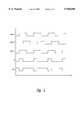
- the leading edge of the external clock CLK signalis aligned with the leading edge of the data signal applied to the D terminal, although the data signal has only a 25% duty cycle. It is common for the data signal to be synchronized to the clock CLK signal before being applied to the integrated circuit 10 because the clock CLK signal may have been used to clock the data out of another integrated circuit (now shown). Primarily because of the capacitive loading of the signal path 12, the delayed clock CLK-DEL signal coupled to the NAND gate 22 is delayed by one-quarter of a clock period, or 90°, as illustrated by the third waveform of the timing diagram.
- timing toleranceshave become increasingly severe. This problem is exacerbated by the increasing complexity in contemporary integrated circuits which require a large number of events to be accurately timed with respect to each other. These timing constraints threaten to create a significant road block to increasing the operating speeds of many conventional integrated circuits.
- the inventive clock generatoris adapted for use in an integrated circuit in which an external clock is coupled to a plurality of internal circuits with significant delays that impair the operation of at least some of the internal circuits.
- the integrated circuitmay be a dynamic random access memory or some other digital circuit.
- the clock generatoruses the delayed external clock signal to generate an internal clock signal that is synchronized to the undelayed external clock signal.
- the clock generatorgenerates the internal clock signal using a phase-lock loop which includes a phase detector receiving the delayed external clock signal and the internal clock signal. The phase detector determines the difference in phase between the delayed external clock signal and the internal clock signal. This phase comparison is then adjusted by a phase offset corresponding to the difference between the phase of the external clock signal and the phase of the delayed external clock signal.
- the phase-lock looppreferably includes a voltage controlled oscillator ("VCO") generating the internal clock signal at a frequency determined by a frequency control signal, and a loop filter generating the frequency control signal from a signal corresponding to the adjusted phase comparison.
- VCOvoltage controlled oscillator
- the clock circuitmay also include a storage device storing data indicative of one of a plurality of predetermined frequency ranges of the external clock signal. The stored data is then used to cause the VCO to operate in one of a plurality of discrete frequency bands corresponding, respectively, to the predetermined frequency ranges.
- the frequency and phase of the internal clock signalneed only be controlled responsive to the adjusted phase comparison in a relatively narrow band of frequencies in the frequency range corresponding to the data from the storage device.
- FIG. 1is a block diagram of a prior art integrated circuit in which an external clock signal is excessively delayed while being coupled to a circuit using the external clock signal.
- FIG. 2is a timing diagram showing various signals present in the integrated circuit of FIG. 1.
- FIG. 3is a block diagram and schematic of a preferred embodiment of the invention in which an internal clock signal is synchronized to an external clock signal despite significant delays in the external clock being coupled to a clock generator generating the internal clock signal.
- FIG. 4is a timing diagram showing various signals present in the integrated circuit of FIG. 3.
- the preferred embodiment of the inventionis exemplified in an integrated circuit 30 shown in FIG. 3.
- the integrated circuitavoids the external clock delay problems of the prior art by creating an internal clock from the delayed external clock signal.
- the phase of the internal clock signalis offset from the delayed external clock signal so that corresponding portions of the internal clock signal actually occur before the corresponding portions of the delayed external signal.
- This phase offsetcorresponds to the delay of the external signal as it is coupled to internal circuits so that the internal clock is substantially synchronized with the external clock.
- the external clock CLK-E signalis applied to the exemplary circuits 14a-n.
- the circuits 14a-nmay be any of a wide variety of conventional or hereinafter developed circuits such as, for example, circuits commonly found in dynamic random access memories.
- the integrated circuit 30will be considered to be a dynamic random access memory device.
- the external clock CLK-E signalis also applied to a phase-lock loop 34 which includes a conventional phase detector 36, a conventional high gain differential amplifier 38, a loop filter 40, and a conventional VCO 42.
- the output of the voltage control oscillatoris an internal clock CLK-I signal that is fed back to the phase detector 36.
- the phase detector 36compares the phase of the delayed clock CLK-D signal with the phase of the internal clock CLK-I signal and generates a resulting error E signal corresponding to the phase difference.
- the error E signalis applied through a resistor 50 to a summing junction 52 of the differential amplifier 38. Also coupled to the summing junction 52 is a negative feedback signal coupled through resistor 56 from the output of the differential amplifier 38, and an offset voltage V applied through a resistor 58.
- the noninverting input of the differential amplifier 38is coupled to ground through a resistor 60.
- the differential amplifier 38generates an output O signal that is proportional to the difference between the error E signal weighted by the ratio of the resistor 56 to the resistor 50 and the offset voltage V weighted by the ratio of the resistor 56 to the resistor 58.
- the output of the differential amplifier 38would be equal to the weighted value of the offset voltage V.
- the difference between the phase of the delayed clock CLK-D signal and the phase of the internal clock CLK-I signalwould correspond to the weighted value of the offset voltage V. The significance of this characteristic will be subsequently apparent.
- the output of the differential amplifier 38is applied to a loop filter 40 which controls the loop dynamics of the phase-lock loop 34.
- a loop filter 40which controls the loop dynamics of the phase-lock loop 34.
- the design of suitable loop filters 40is well within the ability of those skilled in the art and will depend upon a variety of operating parameters.
- the output of the loop filter 40is applied to a frequency control input of the VCO 42 which generates the internal clock CLK-I signal.
- the frequency of the internal clock CLK-I signalis determined by the value of the voltage from the loop filter 40.
- the VCO 42also includes a frequency band select signal f 0 which will be explained below but will be ignored for the present.
- the gain of the phase-lock loop 34is sufficient so that the frequency of the internal clock CLK-I signal is identical to the frequency of the delayed clock CLK-D signal, and the phase of the internal clock CLK-I signal is offset from the phase of the delayed clock CLK-D signal by a magnitude corresponding to the weighted offset voltage V.
- the gain of the phase-lock loop 34is sufficient so that the VCO 42 will be adjusted so that the output of the differential amplifier 38 approaches 0 volts.
- the weighted value of the error E signalmust correspond to the weighted value of the offset voltage V.
- the weighted value of the offset voltage Vis selected so that the phase difference in the signals applied to the phase detector 36 corresponds to the delay of the external clock CLK-E signal as it is coupled to the external circuitry, i.e., the phase difference between the CLK-E signal and the CLK-D signal.
- the external clock CLK-E signalis delayed by one-quarter clock period, or 90°, as it is coupled from the external terminal to the internal circuits 14a-n.
- the data signalis applied to the D terminal of the integrated circuit 30 and is coupled to a NAND gate 70.
- the NAND gate 70is gated by the internal clock CLK-I signal from the VCO 42.
- the internal clock CLK-I signaloccurs one-quarter clock period or 90° before the delayed clock CLK-D signal so that the internal clock CLK-I signal is synchronized to the external clock CLK-E signal at the external terminals of the integrated circuit.
- the internal clock CLK-I signalis able to clock the entire data D signal through the NAND gate 70.
- the signal OUT at the output of the NAND gate 70goes low during the entire portion of the data signal D.
- the VCO 42should be constructed so that it is switched to operate in different frequency bands. By operating in different frequency bands or ranges, it is only necessary for the output of the loop filter 40 to tune the frequency of the internal clock CLK-I signal over a relatively narrow range, thereby minimizing "phase jitter.” Phase jitter occurs from noise on the signal applied to the frequency control input of the VCO 42 from the loop filter 40. Basically, a larger change in VCO frequency output for a given change in control voltage will result in greater phase jitter when the phase-lock loop 34 is locked.
- the frequency band of the VCO 42is selected by a data signal from a speed register 74 which contains data indicative of the frequency of the external clock signals CLK-E.
- the datamay be loaded into the speed register 74 through a conventional input device 76, such as a keyboard. Alternatively, the data may be recorded in the speed register 74 by other means.
- the speed register 74includes a plurality of storage cells 78a-f corresponding to respective allowable frequencies of the external clock CLK-E signal. Only one of the storage cells 78C contains a bit, i.e., logic "1", designating its respective frequency as the frequency of the external clock CLK-E signal.
- the preferred embodiment of the invention 30 illustrated in FIG. 3is thus able to compensate for the significant delays of the external clock CLK-E signal as it is coupled through the integrated circuit 30.
Landscapes
- Physics & Mathematics (AREA)
- Engineering & Computer Science (AREA)
- Theoretical Computer Science (AREA)
- Nonlinear Science (AREA)
- General Engineering & Computer Science (AREA)
- General Physics & Mathematics (AREA)
- Stabilization Of Oscillater, Synchronisation, Frequency Synthesizers (AREA)
- Dram (AREA)
Abstract
Description
This invention relates to clock circuits for generating a clock signal, and, more particularly, to a clock circuit for generating an internal clock signal for an integrated circuit that is synchronized to an external clock signal despite delays in coupling the external clock signal to the clock circuit.
The preferred embodiment of the invention is specially adapted to solve an increasing problem in high-speed integrated circuits in which an externally applied clock is intended to be registered with other signals present in the integrated circuit. The external clock is frequently applied to a large number of circuits so that their operation can be synchronized to each other. As a result, the signal path to which the external clock signal is applied is capacitively loaded to a far greater degree than signal paths receiving other signals. As a result of this heavy capacitive loading, the external clock signal may be delayed significantly before it reaches the internal circuits in the integrated circuit. This delay may be so significant that the delayed external clock signal fails to be properly registered with other signals.
The above-described problem is exemplified by the integratedcircuit 10 shown in FIG. 1. The integratedcircuit 10 may be any of a wide variety of digital circuits including DRAMs, SRAMs, bus bridges, etc. that receives an external clock CLK signal and a data signal D, in addition to a large number of other signals which have been omitted for the purpose of brevity and clarity. The clock signal is coupled through asignal path 12 to a number ofcircuits circuits 14a-n can be any of a variety of circuits conventionally used in integrated circuits. The externally applied clock CLK signal is often used to synchronize the entire operation of the integratedcircuit 10 and is thus typically routed to a large number of circuit nodes. As a result, the capacitive loading on thesignal path 12 is relatively high. In particular, the capacitive loading on thesignal path 12 will often be far higher than the capacitive loading on adata path 20 extending from an external terminal D to a far fewer number of signal nodes or to a single node which, in this example, is aNAND gate 22. As a result, there is relatively little delay of the data signal as it is coupled from the D terminal to theNAND gate 22 compared to the delay of the clock signal as it is coupled to theNAND gate 22 and theother circuits 14a-n. Because of this delay, the clock input to theNAND gate 22 is designated a delayed clock CLK-DEL.
The operation of theexemplary circuit 10 shown in FIG. 1 is best explained with further reference to the timing diagram of FIG. 2. As shown in FIG. 2, the leading edge of the external clock CLK signal is aligned with the leading edge of the data signal applied to the D terminal, although the data signal has only a 25% duty cycle. It is common for the data signal to be synchronized to the clock CLK signal before being applied to the integratedcircuit 10 because the clock CLK signal may have been used to clock the data out of another integrated circuit (now shown). Primarily because of the capacitive loading of thesignal path 12, the delayed clock CLK-DEL signal coupled to theNAND gate 22 is delayed by one-quarter of a clock period, or 90°, as illustrated by the third waveform of the timing diagram. As a result, by the time the CLK-DEL signal has gone high, the data signal has gone low so that the output OUT signal remains high. Thus, because of the delay of the external clock, the external clock signal is ineffective in clocking the data through theNAND gate 22.
As clock speeds continue to increase, timing tolerances have become increasingly severe. This problem is exacerbated by the increasing complexity in contemporary integrated circuits which require a large number of events to be accurately timed with respect to each other. These timing constraints threaten to create a significant road block to increasing the operating speeds of many conventional integrated circuits.
The inventive clock generator is adapted for use in an integrated circuit in which an external clock is coupled to a plurality of internal circuits with significant delays that impair the operation of at least some of the internal circuits. The integrated circuit may be a dynamic random access memory or some other digital circuit. The clock generator uses the delayed external clock signal to generate an internal clock signal that is synchronized to the undelayed external clock signal. The clock generator generates the internal clock signal using a phase-lock loop which includes a phase detector receiving the delayed external clock signal and the internal clock signal. The phase detector determines the difference in phase between the delayed external clock signal and the internal clock signal. This phase comparison is then adjusted by a phase offset corresponding to the difference between the phase of the external clock signal and the phase of the delayed external clock signal. The adjusted phase comparison is then used to control the frequency and phase of the internal clock signal so that the phase of the internal clock signal is substantially the same as the phase of the external clock signal. In addition to the phase detector, the phase-lock loop preferably includes a voltage controlled oscillator ("VCO") generating the internal clock signal at a frequency determined by a frequency control signal, and a loop filter generating the frequency control signal from a signal corresponding to the adjusted phase comparison. The clock circuit may also include a storage device storing data indicative of one of a plurality of predetermined frequency ranges of the external clock signal. The stored data is then used to cause the VCO to operate in one of a plurality of discrete frequency bands corresponding, respectively, to the predetermined frequency ranges. As a result, the frequency and phase of the internal clock signal need only be controlled responsive to the adjusted phase comparison in a relatively narrow band of frequencies in the frequency range corresponding to the data from the storage device.
FIG. 1 is a block diagram of a prior art integrated circuit in which an external clock signal is excessively delayed while being coupled to a circuit using the external clock signal.
FIG. 2 is a timing diagram showing various signals present in the integrated circuit of FIG. 1.
FIG. 3 is a block diagram and schematic of a preferred embodiment of the invention in which an internal clock signal is synchronized to an external clock signal despite significant delays in the external clock being coupled to a clock generator generating the internal clock signal.
FIG. 4 is a timing diagram showing various signals present in the integrated circuit of FIG. 3.
The preferred embodiment of the invention is exemplified in an integratedcircuit 30 shown in FIG. 3. As explained in detail below, the integrated circuit avoids the external clock delay problems of the prior art by creating an internal clock from the delayed external clock signal. Significantly, the phase of the internal clock signal is offset from the delayed external clock signal so that corresponding portions of the internal clock signal actually occur before the corresponding portions of the delayed external signal. This phase offset corresponds to the delay of the external signal as it is coupled to internal circuits so that the internal clock is substantially synchronized with the external clock.
With reference to FIG. 3, the external clock CLK-E signal is applied to theexemplary circuits 14a-n. As in the example of FIG. 1, thecircuits 14a-n may be any of a wide variety of conventional or hereinafter developed circuits such as, for example, circuits commonly found in dynamic random access memories. In face, for purposes of this example, the integratedcircuit 30 will be considered to be a dynamic random access memory device. The external clock CLK-E signal is also applied to a phase-lock loop 34 which includes aconventional phase detector 36, a conventional high gaindifferential amplifier 38, aloop filter 40, and aconventional VCO 42. The output of the voltage control oscillator is an internal clock CLK-I signal that is fed back to thephase detector 36. Thephase detector 36 compares the phase of the delayed clock CLK-D signal with the phase of the internal clock CLK-I signal and generates a resulting error E signal corresponding to the phase difference. The error E signal is applied through aresistor 50 to asumming junction 52 of thedifferential amplifier 38. Also coupled to thesumming junction 52 is a negative feedback signal coupled throughresistor 56 from the output of thedifferential amplifier 38, and an offset voltage V applied through aresistor 58. The noninverting input of thedifferential amplifier 38 is coupled to ground through aresistor 60.
As is well known in the art, thedifferential amplifier 38 generates an output O signal that is proportional to the difference between the error E signal weighted by the ratio of theresistor 56 to theresistor 50 and the offset voltage V weighted by the ratio of theresistor 56 to theresistor 58. Thus, if the delayed clock CLK-D signal was synchronized to the internal clock CLK-I signal so that the error E signal was 0, the output of thedifferential amplifier 38 would be equal to the weighted value of the offset voltage V. However, when the output voltage of thedifferential amplifier 38 was substantially 0, the difference between the phase of the delayed clock CLK-D signal and the phase of the internal clock CLK-I signal would correspond to the weighted value of the offset voltage V. The significance of this characteristic will be subsequently apparent.
The output of thedifferential amplifier 38 is applied to aloop filter 40 which controls the loop dynamics of the phase-lock loop 34. The design ofsuitable loop filters 40 is well within the ability of those skilled in the art and will depend upon a variety of operating parameters.
The output of theloop filter 40 is applied to a frequency control input of theVCO 42 which generates the internal clock CLK-I signal. The frequency of the internal clock CLK-I signal is determined by the value of the voltage from theloop filter 40. TheVCO 42 also includes a frequency band select signal f0 which will be explained below but will be ignored for the present.
In operation, the gain of the phase-lock loop 34 is sufficient so that the frequency of the internal clock CLK-I signal is identical to the frequency of the delayed clock CLK-D signal, and the phase of the internal clock CLK-I signal is offset from the phase of the delayed clock CLK-D signal by a magnitude corresponding to the weighted offset voltage V. In other words, the gain of the phase-lock loop 34 is sufficient so that theVCO 42 will be adjusted so that the output of thedifferential amplifier 38 approaches 0 volts. As explained above, in order for the output of thedifferential amplifier 38 to be substantially 0, the weighted value of the error E signal must correspond to the weighted value of the offset voltage V. In order for the error E signal to have a large enough value to correspond to the offset voltage V, there must be a significant phase difference between the delayed clock CLK-D signal and the internal clock CLK-I signal. In operation, the weighted value of the offset voltage V is selected so that the phase difference in the signals applied to thephase detector 36 corresponds to the delay of the external clock CLK-E signal as it is coupled to the external circuitry, i.e., the phase difference between the CLK-E signal and the CLK-D signal.
The operation of the phase-lock loop 34 is best explained further with reference to the timing diagram of FIG. 4. As shown in FIG. 4, the external clock CLK-E signal is delayed by one-quarter clock period, or 90°, as it is coupled from the external terminal to theinternal circuits 14a-n. Once again, the data signal is applied to the D terminal of theintegrated circuit 30 and is coupled to aNAND gate 70. TheNAND gate 70 is gated by the internal clock CLK-I signal from theVCO 42. Thus, as illustrated in FIG. 4, the internal clock CLK-I signal occurs one-quarter clock period or 90° before the delayed clock CLK-D signal so that the internal clock CLK-I signal is synchronized to the external clock CLK-E signal at the external terminals of the integrated circuit. As a result, the internal clock CLK-I signal is able to clock the entire data D signal through theNAND gate 70. Thus, the signal OUT at the output of theNAND gate 70 goes low during the entire portion of the data signal D.
In the event the frequency of the external clock CLK-E signal is expected to vary significantly, theVCO 42 should be constructed so that it is switched to operate in different frequency bands. By operating in different frequency bands or ranges, it is only necessary for the output of theloop filter 40 to tune the frequency of the internal clock CLK-I signal over a relatively narrow range, thereby minimizing "phase jitter." Phase jitter occurs from noise on the signal applied to the frequency control input of theVCO 42 from theloop filter 40. Basically, a larger change in VCO frequency output for a given change in control voltage will result in greater phase jitter when the phase-lock loop 34 is locked. By using aVCO 42 that operates in discrete frequency bands and using the control voltage to tune the frequency of theVCO 42 only within this band, the change in frequency for a given change in the control voltage can be relatively small. Voltage controlledoscillators 42 having these characteristics are conventional and well within the ability of those skilled in the art. The frequency band of theVCO 42 is selected by a data signal from aspeed register 74 which contains data indicative of the frequency of the external clock signals CLK-E. The data may be loaded into thespeed register 74 through aconventional input device 76, such as a keyboard. Alternatively, the data may be recorded in thespeed register 74 by other means. Preferably, thespeed register 74 includes a plurality ofstorage cells 78a-f corresponding to respective allowable frequencies of the external clock CLK-E signal. Only one of the storage cells 78C contains a bit, i.e., logic "1", designating its respective frequency as the frequency of the external clock CLK-E signal.
The preferred embodiment of theinvention 30 illustrated in FIG. 3 is thus able to compensate for the significant delays of the external clock CLK-E signal as it is coupled through theintegrated circuit 30.
From the foregoing it will be appreciated that, although specific embodiments of the invention have been described herein for purposes of illustration, various modifications may be made without deviating from the spirit and scope of the invention. For example, although the preferred embodiment of the invention uses a phase-lock look, it will be understood that other techniques may be used, including a delay-lock loop or some other means of generating an internal clock signal from the delayed external clock signal in which the phase of the internal clock signal is substantially the same as the external clock signal. Similarly, although the preferred embodiment of the invention has been explained for illustrative purposes as part of a synchronous or aesynchronous dynamic random access memory, it will be understood that it may be used as a part of other integrated circuit devices. Accordingly, the invention is not limited except as by the appended claims.
Claims (27)
1. In an integrated circuit having a plurality of internal circuits receiving a clock signal coupled to the internal circuits from an external clock signal, the clock signal coupled to the internal circuits being delayed relative to the external clock signal, a clock circuit for generating from the delayed external clock signal an internal clock signal that is synchronized to the external clock signal, comprising:
a voltage controlled oscillator ("VCO") generating an output signal having a frequency determined by a frequency control signal, the internal clock signal being derived from the VCO output signal;
a phase detector receiving the delayed external clock signal and the VCO output signal and generating an error signal corresponding to the difference in phase between the delayed external clock signal and the VCO output signal;
a differential amplifier receiving the error signal and a phase adjustment signal and generating an output signal corresponding to the combination of the error signal and the phase adjustment signal, the phase adjustment signal corresponding to the difference between the phase of the external clock signal and the phase of the delayed external clock signal; and
a loop filter receiving the output signal from the differential amplifier, the loop filter generating the frequency control signal from the differential amplifier output signal, the VCO, phase detector, differential amplifier, and loop filter being connected as a phase-lock loop so that the internal clock signal is synchronized to the external clock signal.
2. The clock circuit of claim 1, further comprising:
a storage device storing data indicative of one of a plurality of predetermined frequency ranges of the external clock signal; and
wherein the VCO is operable in each of a plurality of discrete frequency bands corresponding, respectively, to each of the predetermined frequency ranges and wherein the frequency of the VCO output signal is tunable within each of the frequency bands responsive to the frequency control signal, the VCO being coupled to the storage device to receive the frequency range data from the storage device and to operate the VCO in a frequency band corresponding to the data from the storage device.
3. The clock circuit of claim 1, wherein the storage device comprises a programmable register, and wherein the clock circuit further comprises an input device adapted to input the frequency range data into the register.
4. The clock circuit of claim 3, wherein the register comprises a plurality of storage cells each corresponding to one of the plurality of predetermined frequency ranges, and wherein the register is programmed by storing a predetermined data bit in only one of the storage cells.
5. The clock circuit of claim 1, wherein the internal circuits of the integrated circuit comprise a dynamic random access memory.
6. In an integrated circuit having a plurality of internal circuits receiving a clock signal coupled to the internal circuits from an external clock signal, the clock signal coupled to the internal circuits being delayed relative to the external clock signal, a clock circuit for generating from the delayed external clock signal an internal clock signal that is synchronized to the external clock signal, comprising:
a locked loop generating the internal clock signal, the locked loop including a phase detector receiving the delayed external clock signal and the internal clock signal and controlling the frequency and phase of the internal clock signal responsive to the difference in phase between the delayed external clock signal and the internal clock signal; and
an offset circuit producing a predetermined offset between the phase of the internal clock signal and the phase of the delayed external clock signal when the locked loop is locked, the predetermined offset corresponding to the difference between the phase of the external clock signal and the phase of the delayed external clock signal so that the phase of the internal clock signal is substantially the same as the phase of the external clock signal.
7. The clock circuit of claim 6, wherein the locked loop comprises a phase-lock loop.
8. The clock circuit of claim 7, further comprising:
a storage device storing data indicative of one of a plurality of predetermined frequency ranges of the external clock signal; and
a frequency band selector circuit adapted to cause the phase-lock loop to operate in one of a plurality of discrete frequency bands corresponding, respectively, to the predetermined frequency ranges, the frequency band selector circuit being coupled to the storage device to receive the frequency range data from the storage device and to operate the phase-lock loop in a frequency band corresponding to the data from the storage device.
9. The clock circuit of claim 8, wherein the storage device comprises a programmable register, and wherein the clock circuit further comprises an input device adapted to input the frequency range data into the register.
10. The clock circuit of claim 9, wherein the register comprises a plurality of storage cells each corresponding to one of the plurality of predetermined frequency ranges, and wherein the register is programmed by storing a predetermined data bit in only one of the storage cells.
11. The clock circuit of claim 6, wherein the internal circuits of the integrated circuit comprise a dynamic random access memory.
12. In an integrated circuit having a plurality of internal circuits receiving a clock signal coupled to the internal circuits from an external clock signal, the clock signal coupled to the internal circuits being delayed relative to the external clock signal, a clock circuit for generating from the delayed external clock signal an internal clock signal that is synchronized to the external clock signal, comprising:
voltage controlled oscillator means for generating a VCO output signal having a frequency determined by a frequency control signal, the internal clock signal being derived from the VCO output signal;
phase detector means for receiving the delayed external clock signal and the VCO output signal and for generating an error signal corresponding to the difference in phase between the delayed external clock signal and the VCO output signal;
differential amplifier means for receiving the error signal and a phase adjustment signal and for generating an output signal corresponding to the combination of the error signal and the phase adjustment signal, the phase adjustment signal corresponding to the difference between the phase of the external clock signal and the phase of the delayed external clock signal; and
loop filter means for receiving the output signal from the differential amplifier, the loop filter means generating the frequency control signal from the differential amplifier output signal, the voltage controlled oscillator means, phase detector means, differential amplifier means, and loop filter means being connected as a phase-lock loop so that the internal clock signal is synchronized to the external clock signal.
13. The clock circuit of claim 12, further comprising:
storage means for storing data indicative of one of a plurality of predetermined frequency ranges of the external clock signal; and
wherein the voltage controlled oscillator means is operable in each of a plurality of discrete frequency bands corresponding, respectively, to each of the predetermined frequency ranges and wherein the frequency of the VCO output signal is tunable within each of the frequency bands responsive to the frequency control signal, the voltage controlled oscillator means being coupled to the storage means to receive the frequency range data from the storage means and to operate the voltage controlled oscillator means in a frequency band corresponding to the data from the storage means.
14. The clock circuit of claim 12, wherein the storage means comprises programmable register means, and wherein the clock circuit further comprises input means for inputting the frequency range data into the register means.
15. The clock circuit of claim 14, wherein the register means comprises a plurality of storage cells each corresponding to one of the plurality of predetermined frequency ranges, and wherein the register means is programmed by storing a predetermined data bit in only one of the storage cells.
16. The clock circuit of claim 12, wherein the internal circuits of the integrated circuit comprise a dynamic random access memory.
17. An integrated circuit, comprising:
a plurality of internal circuits receiving an external clock signal coupled to the internal circuits from an external clock terminal, the external clock signal being delayed as it is coupled to the internal circuits so that the internal circuits receive a delayed external clock signal; and
a clock circuit for generating from the delayed external clock signal an internal clock signal that is synchronized to the external clock signal, the clock circuit including a phase-adjusting circuit receiving the delayed external clock signal, the phase-adjusting circuit being operative to generate as the internal clock signal a signal derived by adjusting the phase of the delayed external clock signal by the difference in phase between the external clock signal and the delayed external clock signal.
18. The clock circuit of claim 17, wherein the phase adjusting circuit comprises a phase-lock loop generating the internal clock signal, the phase-lock loop having a phase detector comparing the phase of the delayed external clock signal with the phase of the internal clock signal, and an adjusting circuit adjusting the phase of the internal clock signal so that the phase of the delayed external clock signal is delayed relative to the phase of the internal clock signal by the difference in phase between the external clock signal and the delayed external clock signal.
19. A dynamic random access memory receiving an external clock signal, comprising:
a plurality of first dynamic random access memory circuits to which the external clock signal is coupled, the external clock signal being delayed as it is coupled to the dynamic random access memory circuits so that the first dynamic random access memory circuits receive a delayed external clock signal;
a second dynamic random access memory circuit adapted to receive an internal clock signal that is synchronized to the external clock signal;
a phase-lock loop generating the internal clock signal, the phase-lock loop including a phase detector receiving the delayed external clock signal and the internal clock signal and controlling the frequency of the internal clock signal responsive to the difference in phase between the delayed external clock signal and the internal clock signal; and
an offset circuit producing a predetermined offset between the phase of the internal clock signal and the phase of the delayed external clock signal when the phase-lock loop is locked, the predetermined offset corresponding to the difference between the phase of the external clock signal and the phase of the delayed external clock signal so that the phase of the internal clock signal is substantially the same as the phase of the external clock signal.
20. The dynamic random access memory of claim 19, further comprising:
a storage device storing data indicative of one of a plurality of predetermined frequency ranges of the external clock signal; and
a frequency band selector circuit adapted to cause the phase-lock loop to operate in one of a plurality of discrete frequency bands corresponding, respectively, to the predetermined frequency ranges, the frequency band selector circuit being coupled to the storage device to receive the frequency range data from the storage device and to operate the phase-lock loop in a frequency band corresponding to the data from the storage device.
21. The dynamic random access memory of claim 20, wherein the storage device comprises a programmable register, and wherein the clock circuit further comprises an input device adapted to input the frequency range data into the register.
22. The dynamic random access memory of claim 21, wherein the register comprises a plurality of storage cells each corresponding to one of the plurality of predetermined frequency ranges, and wherein the register is programmed by storing a predetermined data bit in only one of the storage cells.
23. A dynamic random access memory receiving an external clock signal, comprising:
a plurality of first dynamic random access memory circuits to which the external clock signal is coupled, the external clock signal being delayed as it is coupled to the dynamic random access memory circuits so that the first dynamic random access memory circuits receive a delayed external clock signal;
a second dynamic random access memory circuit adapted to receive an internal clock signal that is synchronized to the external clock signal;
a phase-adjusting circuit receiving the delayed external clock signal, the phase-adjusting circuit generating as the internal clock signal a signal derived by adjusting the phase of the delayed external clock signal by the difference in phase between the external clock signal and the delayed external clock signal.
24. The dynamic random access memory of claim 23, wherein the phase adjusting circuit comprises a phase-lock loop generating the internal clock signal, the phase-lock loop having a phase detector comparing the phase of the delayed external clock signal with the phase of the internal clock signal, and an adjusting circuit adjusting the phase of the internal clock signal so that the phase of the delayed external clock signal is delayed relative to the phase of the internal clock signal by the difference in phase between the external clock signal and the delayed external clock signal.
25. A method of generating an internal clock signal synchronized to an external clock signal that is coupled to a plurality of circuits in an integrated circuit, the external clock signal being delayed as it is coupled to the circuits so that the circuits receive a delayed external clock signal, the method comprising:
comparing the phase of the delayed external clock signal to the phase of the internal clock signal;
offsetting the comparison of the phase of the delayed external clock signal to the phase of the internal clock signal by a phase offset corresponding to the difference between the phase of the external clock signal and the phase of the delayed external clock signal; and
generating as the internal clock signal a signal having a frequency and a phase determined by the offset comparison between the phase of the delayed external clock signal and the phase of the internal clock signal.
26. The method of claim 25, further comprising:
storing data indicative of one of a plurality of predetermined frequency ranges of the external clock signal;
selecting one of a plurality of discrete frequency bands of the internal clock signal corresponding, respectively, to the predetermined frequency ranges, the discrete frequency band being selected based on the stored frequency range data; and
adjusting the phase and frequency of the internal clock signal within the selected frequency band as a function of the offset comparison between the phase of the delayed external clock signal and the phase of the internal clock signal.
27. The method of claim 25, wherein the circuits in the integrated circuit comprise a dynamic random access memory.
Priority Applications (7)
| Application Number | Priority Date | Filing Date | Title |
|---|---|---|---|
| US08/798,226US5940608A (en) | 1997-02-11 | 1997-02-11 | Method and apparatus for generating an internal clock signal that is synchronized to an external clock signal |
| KR1019997007266AKR100660760B1 (en) | 1997-02-11 | 1998-02-11 | Clock Circuits, Dynamic Random Access Memory, and Internal Clock Signal Generation Methods |
| JP53489398AJP3947231B2 (en) | 1997-02-11 | 1998-02-11 | Method and apparatus for generating an internal clock signal synchronized with an external clock signal |
| PCT/US1998/002233WO1998035445A1 (en) | 1997-02-11 | 1998-02-11 | Method and apparatus for generating an internal clock signal that is synchronized to an external clock signal |
| AU62699/98AAU6269998A (en) | 1997-02-11 | 1998-02-11 | Method and apparatus for generating an internal clock signal that is synchronized to an external clock signal |
| US09/317,059US6340904B1 (en) | 1997-02-11 | 1999-05-24 | Method and apparatus for generating an internal clock signal that is synchronized to an external clock signal |
| JP2007041506AJP2007151183A (en) | 1997-02-11 | 2007-02-21 | Method and apparatus for generating internal clock signal that is synchronized to external clock signal |
Applications Claiming Priority (1)
| Application Number | Priority Date | Filing Date | Title |
|---|---|---|---|
| US08/798,226US5940608A (en) | 1997-02-11 | 1997-02-11 | Method and apparatus for generating an internal clock signal that is synchronized to an external clock signal |
Related Child Applications (1)
| Application Number | Title | Priority Date | Filing Date |
|---|---|---|---|
| US09/317,059ContinuationUS6340904B1 (en) | 1997-02-11 | 1999-05-24 | Method and apparatus for generating an internal clock signal that is synchronized to an external clock signal |
Publications (1)
| Publication Number | Publication Date |
|---|---|
| US5940608Atrue US5940608A (en) | 1999-08-17 |
Family
ID=25172852
Family Applications (2)
| Application Number | Title | Priority Date | Filing Date |
|---|---|---|---|
| US08/798,226Expired - LifetimeUS5940608A (en) | 1997-02-11 | 1997-02-11 | Method and apparatus for generating an internal clock signal that is synchronized to an external clock signal |
| US09/317,059Expired - LifetimeUS6340904B1 (en) | 1997-02-11 | 1999-05-24 | Method and apparatus for generating an internal clock signal that is synchronized to an external clock signal |
Family Applications After (1)
| Application Number | Title | Priority Date | Filing Date |
|---|---|---|---|
| US09/317,059Expired - LifetimeUS6340904B1 (en) | 1997-02-11 | 1999-05-24 | Method and apparatus for generating an internal clock signal that is synchronized to an external clock signal |
Country Status (5)
| Country | Link |
|---|---|
| US (2) | US5940608A (en) |
| JP (2) | JP3947231B2 (en) |
| KR (1) | KR100660760B1 (en) |
| AU (1) | AU6269998A (en) |
| WO (1) | WO1998035445A1 (en) |
Cited By (51)
| Publication number | Priority date | Publication date | Assignee | Title |
|---|---|---|---|---|
| WO2000033464A1 (en)* | 1998-12-02 | 2000-06-08 | Tait Electronics Limited | Improvements relating to phase lock loops |
| US6209106B1 (en)* | 1998-09-30 | 2001-03-27 | International Business Machines Corporation | Method and apparatus for synchronizing selected logical partitions of a partitioned information handling system to an external time reference |
| US6256259B1 (en) | 1997-03-05 | 2001-07-03 | Micron Technology, Inc. | Delay-locked loop with binary-coupled capacitor |
| US6269451B1 (en)* | 1998-02-27 | 2001-07-31 | Micron Technology, Inc. | Method and apparatus for adjusting data timing by delaying clock signal |
| US6279090B1 (en) | 1998-09-03 | 2001-08-21 | Micron Technology, Inc. | Method and apparatus for resynchronizing a plurality of clock signals used in latching respective digital signals applied to a packetized memory device |
| US6316979B1 (en) | 1998-03-20 | 2001-11-13 | Micron Technology, Inc. | Integrated circuit data latch driver circuit |
| US6321282B1 (en) | 1999-10-19 | 2001-11-20 | Rambus Inc. | Apparatus and method for topography dependent signaling |
| US6338127B1 (en) | 1998-08-28 | 2002-01-08 | Micron Technology, Inc. | Method and apparatus for resynchronizing a plurality of clock signals used to latch respective digital signals, and memory device using same |
| US6349399B1 (en)* | 1998-09-03 | 2002-02-19 | Micron Technology, Inc. | Method and apparatus for generating expect data from a captured bit pattern, and memory device using same |
| US6374360B1 (en) | 1998-12-11 | 2002-04-16 | Micron Technology, Inc. | Method and apparatus for bit-to-bit timing correction of a high speed memory bus |
| US20020049936A1 (en)* | 2000-07-31 | 2002-04-25 | Vadim Gutnik | Clock distribution circuits and methods of operating same that use multiple clock circuits connected by phase detector circuits to generate and synchronize local clock signals |
| US6415390B1 (en) | 1998-06-23 | 2002-07-02 | Micron Technology, Inc. | Method and apparatus for controlling the data rate of a clocking circuit |
| US6430696B1 (en) | 1998-11-30 | 2002-08-06 | Micron Technology, Inc. | Method and apparatus for high speed data capture utilizing bit-to-bit timing correction, and memory device using same |
| US6448756B1 (en)* | 2000-08-30 | 2002-09-10 | Micron Technology, Inc. | Delay line tap setting override for delay locked loop (DLL) testability |
| US6516006B1 (en)* | 1999-02-16 | 2003-02-04 | Mitsubishi Electric And Electronics U.S.A., Inc. | Self-adjusting clock phase controlled architecture |
| US20030062547A1 (en)* | 2001-09-28 | 2003-04-03 | Eckhard Brass | Semiconductor memory device |
| US6570813B2 (en) | 2001-05-25 | 2003-05-27 | Micron Technology, Inc. | Synchronous mirror delay with reduced delay line taps |
| US20030117864A1 (en)* | 2001-10-22 | 2003-06-26 | Hampel Craig E. | Phase adjustment apparatus and method for a memory device signaling system |
| US20030179027A1 (en)* | 2002-03-22 | 2003-09-25 | Kizer Jade M. | Locked loop with dual rail regulation |
| US20030183842A1 (en)* | 2002-03-22 | 2003-10-02 | Kizer Jade M. | System with phase jumping locked loop circuit |
| US20030188215A1 (en)* | 2002-03-26 | 2003-10-02 | Semtech Corporation | Method and apparatus for controlling the phase of the clock output of a digital clock |
| US6643787B1 (en) | 1999-10-19 | 2003-11-04 | Rambus Inc. | Bus system optimization |
| US6657917B2 (en) | 2001-07-02 | 2003-12-02 | Micron Technology, Inc. | Selective adjustment of voltage controlled oscillator gain in a phase-locked loop |
| US20030231537A1 (en)* | 1999-10-19 | 2003-12-18 | Stark Donald C. | Single-clock, strobeless signaling system |
| US20040041604A1 (en)* | 2002-09-03 | 2004-03-04 | Kizer Jade M. | Phase jumping locked loop circuit |
| US20040066222A1 (en)* | 2002-10-04 | 2004-04-08 | Mcwilliams John | Non-iterative introduction of phase delay into signal without feedback |
| US20040150446A1 (en)* | 2003-02-04 | 2004-08-05 | Cray Inc. | Systems and methods for phase detector circuit with reduced offset |
| US6798259B2 (en) | 2001-08-03 | 2004-09-28 | Micron Technology, Inc. | System and method to improve the efficiency of synchronous mirror delays and delay locked loops |
| US6801989B2 (en) | 2001-06-28 | 2004-10-05 | Micron Technology, Inc. | Method and system for adjusting the timing offset between a clock signal and respective digital signals transmitted along with that clock signal, and memory device and computer system using same |
| US20050030344A1 (en)* | 2003-08-07 | 2005-02-10 | Lexmark International, Inc. | Ink jet heater chip with internally generated clock signal |
| US6885228B2 (en) | 2002-10-02 | 2005-04-26 | Hewlett-Packard Development Company, L.P. | Non-iterative signal synchronization |
| US20050122153A1 (en)* | 2003-12-08 | 2005-06-09 | Lin Feng D. | Centralizing the lock point of a synchronous circuit |
| US6912680B1 (en) | 1997-02-11 | 2005-06-28 | Micron Technology, Inc. | Memory system with dynamic timing correction |
| US6922091B2 (en) | 2002-09-03 | 2005-07-26 | Rambus Inc. | Locked loop circuit with clock hold function |
| US6931086B2 (en) | 1999-03-01 | 2005-08-16 | Micron Technology, Inc. | Method and apparatus for generating a phase dependent control signal |
| US6952123B2 (en) | 2002-03-22 | 2005-10-04 | Rambus Inc. | System with dual rail regulated locked loop |
| US6954097B2 (en) | 1997-06-20 | 2005-10-11 | Micron Technology, Inc. | Method and apparatus for generating a sequence of clock signals |
| US6959016B1 (en) | 1997-09-18 | 2005-10-25 | Micron Technology, Inc. | Method and apparatus for adjusting the timing of signals over fine and coarse ranges |
| US20050241196A1 (en)* | 2004-04-27 | 2005-11-03 | Cnh America Llc | Backhoe pivot joint |
| US6992515B1 (en) | 2003-08-18 | 2006-01-31 | Cray, Inc. | Clock signal duty cycle adjust circuit |
| US7051130B1 (en) | 1999-10-19 | 2006-05-23 | Rambus Inc. | Integrated circuit device that stores a value representative of a drive strength setting |
| US20060268655A1 (en)* | 2005-05-26 | 2006-11-30 | Micron Technology, Inc. | Method and system for improved efficiency of synchronous mirror delays and delay locked loops |
| US20060285406A1 (en)* | 2005-06-21 | 2006-12-21 | Micron Technology, Inc. | Input buffer for low voltage operation |
| US7168027B2 (en) | 2003-06-12 | 2007-01-23 | Micron Technology, Inc. | Dynamic synchronization of data capture on an optical or other high speed communications link |
| US7234070B2 (en) | 2003-10-27 | 2007-06-19 | Micron Technology, Inc. | System and method for using a learning sequence to establish communications on a high-speed nonsynchronous interface in the absence of clock forwarding |
| KR100738242B1 (en)* | 1999-10-22 | 2007-07-12 | 프리스케일 세미컨덕터, 인크. | Method and apparatus for a calibrated frequency modulation phase locked loop |
| US20070201596A1 (en)* | 2006-02-28 | 2007-08-30 | Flowers John P | Clock synchronization using early clock |
| US20070273419A1 (en)* | 2002-09-30 | 2007-11-29 | Conway Craig M | Synchronizing measurement devices using trigger signals |
| US20080240321A1 (en)* | 2007-04-02 | 2008-10-02 | Narus Gabriel L | Aligning Timebases to Share Synchronized Periodic Signals |
| US8086100B2 (en) | 2001-02-05 | 2011-12-27 | Finisar Corporation | Optoelectronic transceiver with digital diagnostics |
| US20140068316A1 (en)* | 2012-08-29 | 2014-03-06 | Fujitsu Limited | Determination support apparatus, determining apparatus, memory controller, system, and determination method |
Families Citing this family (20)
| Publication number | Priority date | Publication date | Assignee | Title |
|---|---|---|---|---|
| US6032261A (en)* | 1997-12-30 | 2000-02-29 | Philips Electronics North America Corp. | Bus bridge with distribution of a common cycle clock to all bridge portals to provide synchronization of local buses, and method of operation thereof |
| US6424178B1 (en)* | 2000-08-30 | 2002-07-23 | Micron Technology, Inc. | Method and system for controlling the duty cycle of a clock signal |
| JP2002077125A (en)* | 2000-09-01 | 2002-03-15 | Fujitsu Ltd | Clock synchronization method, clock synchronization circuit, and semiconductor device using the circuit |
| US6930524B2 (en)* | 2001-10-09 | 2005-08-16 | Micron Technology, Inc. | Dual-phase delay-locked loop circuit and method |
| US6759911B2 (en) | 2001-11-19 | 2004-07-06 | Mcron Technology, Inc. | Delay-locked loop circuit and method using a ring oscillator and counter-based delay |
| US6898725B2 (en)* | 2002-03-27 | 2005-05-24 | International Business Machines Corporation | Method for adjusting system clocks using dynamic clock ratio detector to detect clock ratio between clock domain of driver and counting receiver clock domain |
| US6937076B2 (en)* | 2003-06-11 | 2005-08-30 | Micron Technology, Inc. | Clock synchronizing apparatus and method using frequency dependent variable delay |
| KR100542696B1 (en)* | 2003-11-13 | 2006-01-11 | 주식회사 하이닉스반도체 | Repair fuse box of semiconductor device |
| KR100514414B1 (en)* | 2003-11-20 | 2005-09-09 | 주식회사 하이닉스반도체 | Delay locked loop |
| USD511701S1 (en)* | 2004-04-06 | 2005-11-22 | Hioki Denki Kabushiki Kaisha | Phase detector |
| US7130226B2 (en)* | 2005-02-09 | 2006-10-31 | Micron Technology, Inc. | Clock generating circuit with multiple modes of operation |
| US20060248417A1 (en)* | 2005-04-28 | 2006-11-02 | International Business Machines Corporation | Clock control circuit for test that facilitates an at speed structural test |
| US7487315B2 (en)* | 2005-09-14 | 2009-02-03 | Via Technologies, Inc. | Accessing apparatus capable of reducing power consumption and accessing method thereof |
| US7199625B1 (en)* | 2005-09-20 | 2007-04-03 | Infineon Technologies Ag | Delay locked loop structure providing first and second locked clock signals |
| KR100738960B1 (en)* | 2006-02-22 | 2007-07-12 | 주식회사 하이닉스반도체 | Phase locked loop and control method of the same |
| US7405604B2 (en)* | 2006-04-20 | 2008-07-29 | Realtek Semiconductor Corp. | Variable delay clock circuit and method thereof |
| US7551011B2 (en)* | 2006-08-10 | 2009-06-23 | Ameritherm, Inc. | Constant phase angle control for frequency agile power switching systems |
| KR100864853B1 (en) | 2007-03-14 | 2008-10-23 | 포항공과대학교 산학협력단 | PLL with short settling time and frequency and phase stabilization method with short settling time and PLL using the method |
| US9325489B2 (en)* | 2013-12-19 | 2016-04-26 | Xilinx, Inc. | Data receivers and methods of implementing data receivers in an integrated circuit |
| CN113452353B (en)* | 2021-06-29 | 2023-06-09 | 深圳市长运通半导体技术有限公司 | Oscillator with adjustable frequency and external synchronous clock function |
Citations (104)
| Publication number | Priority date | Publication date | Assignee | Title |
|---|---|---|---|---|
| US3633174A (en)* | 1970-04-14 | 1972-01-04 | Us Navy | Memory system having self-adjusting strobe timing |
| US4077016A (en)* | 1977-02-22 | 1978-02-28 | Ncr Corporation | Apparatus and method for inhibiting false locking of a phase-locked loop |
| US4096402A (en)* | 1975-12-29 | 1978-06-20 | Mostek Corporation | MOSFET buffer for TTL logic input and method of operation |
| US4404474A (en)* | 1981-02-06 | 1983-09-13 | Rca Corporation | Active load pulse generating circuit |
| US4511846A (en)* | 1982-05-24 | 1985-04-16 | Fairchild Camera And Instrument Corporation | Deskewing time-critical signals in automatic test equipment |
| US4514647A (en)* | 1983-08-01 | 1985-04-30 | At&T Bell Laboratories | Chipset synchronization arrangement |
| US4600895A (en)* | 1985-04-26 | 1986-07-15 | Minnesota Mining And Manufacturing Company | Precision phase synchronization of free-running oscillator output signal to reference signal |
| US4638187A (en)* | 1985-10-01 | 1987-01-20 | Vtc Incorporated | CMOS output buffer providing high drive current with minimum output signal distortion |
| US4687951A (en)* | 1984-10-29 | 1987-08-18 | Texas Instruments Incorporated | Fuse link for varying chip operating parameters |
| US4773085A (en)* | 1987-06-12 | 1988-09-20 | Bell Communications Research, Inc. | Phase and frequency detector circuits |
| US4789796A (en)* | 1985-12-23 | 1988-12-06 | U.S. Philips Corporation | Output buffer having sequentially-switched output |
| US4893087A (en)* | 1988-01-07 | 1990-01-09 | Motorola, Inc. | Low voltage and low power frequency synthesizer |
| US4902986A (en)* | 1989-01-30 | 1990-02-20 | Asix Systems Corporation | Phased locked loop to provide precise frequency and phase tracking of two signals |
| US4958088A (en)* | 1989-06-19 | 1990-09-18 | Micron Technology, Inc. | Low power three-stage CMOS input buffer with controlled switching |
| US4984204A (en)* | 1988-01-28 | 1991-01-08 | Hitachi, Ltd. | High speed sensor system using a level shift circuit |
| US5020023A (en)* | 1989-02-23 | 1991-05-28 | International Business Machines Corporation | Automatic vernier synchronization of skewed data streams |
| US5038115A (en)* | 1990-05-29 | 1991-08-06 | Myers Glen A | Method and apparatus for frequency independent phase tracking of input signals in receiving systems and the like |
| US5086500A (en)* | 1987-08-07 | 1992-02-04 | Tektronix, Inc. | Synchronized system by adjusting independently clock signals arriving at a plurality of integrated circuits |
| US5087828A (en)* | 1990-02-14 | 1992-02-11 | Daiichi Denshi Kogyo Kabushiki Kaisha | Timing circuit for single line serial data |
| US5122690A (en)* | 1990-10-16 | 1992-06-16 | General Electric Company | Interface circuits including driver circuits with switching noise reduction |
| US5128560A (en)* | 1991-03-22 | 1992-07-07 | Micron Technology, Inc. | Boosted supply output driver circuit for driving an all N-channel output stage |
| US5128563A (en)* | 1990-11-28 | 1992-07-07 | Micron Technology, Inc. | CMOS bootstrapped output driver method and circuit |
| US5134311A (en)* | 1990-06-07 | 1992-07-28 | International Business Machines Corporation | Self-adjusting impedance matching driver |
| US5150186A (en)* | 1991-03-06 | 1992-09-22 | Micron Technology, Inc. | CMOS output pull-up driver |
| US5165046A (en)* | 1989-11-06 | 1992-11-17 | Micron Technology, Inc. | High speed CMOS driver circuit |
| US5179298A (en)* | 1990-01-17 | 1993-01-12 | Matsushita Electric Industrial Co., Ltd. | CMOS buffer circuit which is not influenced by bounce noise |
| US5194765A (en)* | 1991-06-28 | 1993-03-16 | At&T Bell Laboratories | Digitally controlled element sizing |
| US5212601A (en)* | 1991-05-03 | 1993-05-18 | Western Digital Corporation | Disk drive data synchronizer with window shift synthesis |
| US5220208A (en)* | 1991-04-29 | 1993-06-15 | Texas Instruments Incorporated | Circuitry and method for controlling current in an electronic circuit |
| US5239206A (en)* | 1990-03-06 | 1993-08-24 | Advanced Micro Devices, Inc. | Synchronous circuit with clock skew compensating function and circuits utilizing same |
| US5243703A (en)* | 1990-04-18 | 1993-09-07 | Rambus, Inc. | Apparatus for synchronously generating clock signals in a data processing system |
| US5254883A (en)* | 1992-04-22 | 1993-10-19 | Rambus, Inc. | Electrical current source circuitry for a bus |
| US5257294A (en)* | 1990-11-13 | 1993-10-26 | National Semiconductor Corporation | Phase-locked loop circuit and method |
| US5256989A (en)* | 1991-05-03 | 1993-10-26 | Motorola, Inc. | Lock detection for a phase lock loop |
| US5268639A (en)* | 1992-06-05 | 1993-12-07 | Rambus, Inc. | Testing timing parameters of high speed integrated circuit devices |
| US5274276A (en)* | 1992-06-26 | 1993-12-28 | Micron Technology, Inc. | Output driver circuit comprising a programmable circuit for determining the potential at the output node and the method of implementing the circuit |
| US5276642A (en)* | 1991-07-15 | 1994-01-04 | Micron Technology, Inc. | Method for performing a split read/write operation in a dynamic random access memory |
| US5278460A (en)* | 1992-04-07 | 1994-01-11 | Micron Technology, Inc. | Voltage compensating CMOS input buffer |
| US5281865A (en)* | 1990-11-28 | 1994-01-25 | Hitachi, Ltd. | Flip-flop circuit |
| US5283631A (en)* | 1991-11-01 | 1994-02-01 | Hewlett-Packard Co. | Programmable capacitance delay element having inverters controlled by adjustable voltage to offset temperature and voltage supply variations |
| US5295164A (en)* | 1991-12-23 | 1994-03-15 | Apple Computer, Inc. | Apparatus for providing a system clock locked to an external clock over a wide range of frequencies |
| US5311481A (en)* | 1992-12-17 | 1994-05-10 | Micron Technology, Inc. | Wordline driver circuit having a directly gated pull-down device |
| US5321368A (en)* | 1992-02-27 | 1994-06-14 | Siemens Aktiengesellschaft | Synchronized, digital sequential circuit |
| US5337285A (en)* | 1993-05-21 | 1994-08-09 | Rambus, Inc. | Method and apparatus for power control in devices |
| US5347179A (en)* | 1993-04-15 | 1994-09-13 | Micron Semiconductor, Inc. | Inverting output driver circuit for reducing electron injection into the substrate |
| US5347177A (en)* | 1993-01-14 | 1994-09-13 | Lipp Robert J | System for interconnecting VLSI circuits with transmission line characteristics |
| US5355391A (en)* | 1992-03-06 | 1994-10-11 | Rambus, Inc. | High speed bus system |
| US5390308A (en)* | 1992-04-15 | 1995-02-14 | Rambus, Inc. | Method and apparatus for address mapping of dynamic random access memory |
| US5400283A (en)* | 1993-12-13 | 1995-03-21 | Micron Semiconductor, Inc. | RAM row decode circuitry that utilizes a precharge circuit that is deactivated by a feedback from an activated word line driver |
| US5408640A (en)* | 1990-02-21 | 1995-04-18 | Digital Equipment Corporation | Phase delay compensator using gating signal generated by a synchronizer for loading and shifting of bit pattern to produce clock phases corresponding to frequency changes |
| US5410263A (en)* | 1992-05-28 | 1995-04-25 | Intel Corporation | Delay line loop for on-chip clock synthesis with zero skew and 50% duty cycle |
| US5416436A (en)* | 1992-09-22 | 1995-05-16 | Francen Telecom | Method for time delaying a signal and corresponding delay circuit |
| US5420544A (en)* | 1992-12-28 | 1995-05-30 | Mitsubishi Denki Kabushiki Kaisha | Semiconductor integrated circuit, method of designing the same and method of manufacturing the same |
| US5428311A (en)* | 1993-06-30 | 1995-06-27 | Sgs-Thomson Microelectronics, Inc. | Fuse circuitry to control the propagation delay of an IC |
| US5430676A (en)* | 1993-06-02 | 1995-07-04 | Rambus, Inc. | Dynamic random access memory system |
| US5432823A (en)* | 1992-03-06 | 1995-07-11 | Rambus, Inc. | Method and circuitry for minimizing clock-data skew in a bus system |
| US5438545A (en)* | 1993-12-21 | 1995-08-01 | Goldstar Electron Co., Ltd. | Data output buffer of semiconductor memory device for preventing noises |
| US5440514A (en)* | 1994-03-08 | 1995-08-08 | Motorola Inc. | Write control for a memory using a delay locked loop |
| US5440260A (en)* | 1991-08-14 | 1995-08-08 | Advantest Corporation | Variable delay circuit |
| US5446696A (en)* | 1993-05-28 | 1995-08-29 | Rambus, Inc. | Method and apparatus for implementing refresh in a synchronous DRAM system |
| US5448193A (en)* | 1992-11-05 | 1995-09-05 | At&T Corp. | Normalization of apparent propagation delay |
| US5451898A (en)* | 1993-11-12 | 1995-09-19 | Rambus, Inc. | Bias circuit and differential amplifier having stabilized output swing |
| US5457407A (en)* | 1994-07-06 | 1995-10-10 | Sony Electronics Inc. | Binary weighted reference circuit for a variable impedance output buffer |
| US5473639A (en)* | 1993-07-26 | 1995-12-05 | Hewlett-Packard Company | Clock recovery apparatus with means for sensing an out of lock condition |
| US5473274A (en)* | 1992-09-14 | 1995-12-05 | Nec America, Inc. | Local clock generator |
| US5473575A (en)* | 1990-04-18 | 1995-12-05 | Rambus, Inc. | Integrated circuit I/O using a high performance bus interface |
| US5485490A (en)* | 1992-05-28 | 1996-01-16 | Rambus, Inc. | Method and circuitry for clock synchronization |
| US5488321A (en)* | 1993-04-07 | 1996-01-30 | Rambus, Inc. | Static high speed comparator |
| US5497127A (en)* | 1994-12-14 | 1996-03-05 | David Sarnoff Research Center, Inc. | Wide frequency range CMOS relaxation oscillator with variable hysteresis |
| US5498990A (en)* | 1991-11-05 | 1996-03-12 | Monolithic System Technology, Inc. | Reduced CMOS-swing clamping circuit for bus lines |
| US5506814A (en)* | 1993-05-28 | 1996-04-09 | Micron Technology, Inc. | Video random access memory device and method implementing independent two WE nibble control |
| US5508638A (en)* | 1994-02-24 | 1996-04-16 | Micron Technology, Inc. | Low current redundancy fuse assembly |
| US5539345A (en)* | 1992-12-30 | 1996-07-23 | Digital Equipment Corporation | Phase detector apparatus |
| US5552727A (en)* | 1993-10-06 | 1996-09-03 | Mitsubishi Denki Kabushiki Kaisha | Digital phase locked loop circuit |
| US5568077A (en)* | 1994-11-07 | 1996-10-22 | Mitsubishi Denki Kabushiki Kaisha | Latch circuit |
| US5572557A (en)* | 1993-06-02 | 1996-11-05 | Nec Corporation | Semiconductor integrated circuit device including PLL circuit |
| US5577236A (en)* | 1994-12-30 | 1996-11-19 | International Business Machines Corporation | Memory controller for reading data from synchronous RAM |
| US5576645A (en)* | 1995-06-05 | 1996-11-19 | Hughes Aircraft Company | Sample and hold flip-flop for CMOS logic |
| US5578941A (en)* | 1995-08-23 | 1996-11-26 | Micron Technology, Inc. | Voltage compensating CMOS input buffer circuit |
| US5578940A (en)* | 1995-04-04 | 1996-11-26 | Rambus, Inc. | Modular bus with single or double parallel termination |
| US5579326A (en)* | 1994-01-31 | 1996-11-26 | Sgs-Thomson Microelectronics, Inc. | Method and apparatus for programming signal timing |
| US5581197A (en)* | 1995-05-31 | 1996-12-03 | Hewlett-Packard Co. | Method of programming a desired source resistance for a driver stage |
| US5590073A (en)* | 1993-11-30 | 1996-12-31 | Sony Corporation | Random access memory having flash memory |
| US5589788A (en)* | 1994-05-12 | 1996-12-31 | Hewlett-Packard Company | Timing adjustment circuit |
| US5594690A (en)* | 1995-12-15 | 1997-01-14 | Unisys Corporation | Integrated circuit memory having high speed and low power by selectively coupling compensation components to a pulse generator |
| US5614855A (en)* | 1994-02-15 | 1997-03-25 | Rambus, Inc. | Delay-locked loop |
| US5619473A (en)* | 1994-08-23 | 1997-04-08 | Sharp Kabushiki Kaisha | Semiconductor memory device with dual address memory read amplifiers |
| US5621690A (en)* | 1995-04-28 | 1997-04-15 | Intel Corporation | Nonvolatile memory blocking architecture and redundancy |
| US5621739A (en)* | 1996-05-07 | 1997-04-15 | Intel Corporation | Method and apparatus for buffer self-test and characterization |
| US5621340A (en)* | 1995-08-02 | 1997-04-15 | Rambus Inc. | Differential comparator for amplifying small swing signals to a full swing output |
| US5627791A (en)* | 1996-02-16 | 1997-05-06 | Micron Technology, Inc. | Multiple bank memory with auto refresh to specified bank |
| US5627780A (en)* | 1994-08-26 | 1997-05-06 | Sgs-Thomson Microelectronics Limited | Testing a non-volatile memory |
| US5631872A (en)* | 1995-08-14 | 1997-05-20 | Nec Corporation | Low power consumption semiconductor dynamic random access memory device by reusing residual electric charge on bit line pairs |
| US5636173A (en)* | 1995-06-07 | 1997-06-03 | Micron Technology, Inc. | Auto-precharge during bank selection |
| US5636163A (en)* | 1986-07-30 | 1997-06-03 | Mitsubishi Denki Kabushiki Kaisha | Random access memory with a plurality amplifier groups for reading and writing in normal and test modes |
| US5636174A (en)* | 1996-01-11 | 1997-06-03 | Cirrus Logic, Inc. | Fast cycle time-low latency dynamic random access memories and systems and methods using the same |
| US5638335A (en)* | 1995-05-22 | 1997-06-10 | Hitachi, Ltd. | Semiconductor device |
| US5668763A (en) | 1996-02-26 | 1997-09-16 | Fujitsu Limited | Semiconductor memory for increasing the number of half good memories by selecting and using good memory blocks |
| US5692165A (en) | 1995-09-12 | 1997-11-25 | Micron Electronics Inc. | Memory controller with low skew control signal |
| US5694065A (en) | 1994-08-16 | 1997-12-02 | Burr-Brown Corporation | Switching control circuitry for low noise CMOS inverter |
| US5712580A (en) | 1996-02-14 | 1998-01-27 | International Business Machines Corporation | Linear phase detector for half-speed quadrature clocking architecture |
| US5719508A (en) | 1996-02-01 | 1998-02-17 | Northern Telecom, Ltd. | Loss of lock detector for master timing generator |
| US5751665A (en) | 1995-07-14 | 1998-05-12 | Oki Electric Industry Co., Ltd. | Clock distributing circuit |
| US5789947A (en) | 1995-09-21 | 1998-08-04 | Nippon Precision Circuits Inc. | Phase comparator |
Family Cites Families (96)
| Publication number | Priority date | Publication date | Assignee | Title |
|---|---|---|---|---|
| DE2945331C2 (en) | 1979-11-09 | 1984-05-30 | Nixdorf Computer Ag, 4790 Paderborn | Device in a signal or data processing system for setting a signal processing circuit |
| US4481625A (en) | 1981-10-21 | 1984-11-06 | Elxsi | High speed data bus system |
| US4508983A (en) | 1983-02-10 | 1985-04-02 | Motorola, Inc. | MOS Analog switch driven by complementary, minimally skewed clock signals |
| US4603320A (en) | 1983-04-13 | 1986-07-29 | Anico Research, Ltd. Inc. | Connector interface |
| US4638451A (en) | 1983-05-03 | 1987-01-20 | Texas Instruments Incorporated | Microprocessor system with programmable interface |
| US4573017A (en) | 1984-01-03 | 1986-02-25 | Motorola, Inc. | Unitary phase and frequency adjust network for a multiple frequency digital phase locked loop |
| JPH07105818B2 (en) | 1986-05-19 | 1995-11-13 | 株式会社日立製作所 | Parallel transmission method |
| JPS63276795A (en) | 1986-12-16 | 1988-11-15 | Mitsubishi Electric Corp | Variable length shift register |
| JPS63304721A (en)* | 1987-06-05 | 1988-12-13 | Anritsu Corp | Signal generator |
| US4972470A (en) | 1987-08-06 | 1990-11-20 | Steven Farago | Programmable connector |
| US5367649A (en) | 1988-05-20 | 1994-11-22 | Waferscale Integration, Inc. | Programmable controller |
| US4885554A (en)* | 1988-12-16 | 1989-12-05 | Tektronix, Inc. | Phase-offset signal generator |
| US5475631A (en) | 1989-03-09 | 1995-12-12 | Micron Technology, Inc. | Multiport RAM based multiprocessor |
| US5075569A (en) | 1989-03-17 | 1991-12-24 | Tektronix, Inc. | Output device circuit and method to minimize impedance fluctuations during crossover |
| IT1236578B (en) | 1989-07-04 | 1993-03-16 | Ind Face Standard S P A Milano | Type D flip=flop to type B flip=flop converter circuit |
| US5023488A (en) | 1990-03-30 | 1991-06-11 | Xerox Corporation | Drivers and receivers for interfacing VLSI CMOS circuits to transmission lines |
| JP3426608B2 (en) | 1990-04-04 | 2003-07-14 | ユニシス コーポレイシヨン | Clock deskew circuit |
| DE69116230T2 (en) | 1990-06-08 | 1996-07-04 | Toshiba Kawasaki Kk | Semiconductor memory with error handling circuit |
| US5416909A (en) | 1990-09-14 | 1995-05-16 | Vlsi Technology, Inc. | Input/output controller circuit using a single transceiver to serve multiple input/output ports and method therefor |
| EP0476585B1 (en) | 1990-09-18 | 1998-08-26 | Fujitsu Limited | Electronic device using a reference delay generator |
| JP2740063B2 (en) | 1990-10-15 | 1998-04-15 | 株式会社東芝 | Semiconductor storage device |
| TW198135B (en) | 1990-11-20 | 1993-01-11 | Oki Electric Ind Co Ltd | |
| US5223755A (en) | 1990-12-26 | 1993-06-29 | Xerox Corporation | Extended frequency range variable delay locked loop for clock synchronization |
| US5500808A (en) | 1991-01-24 | 1996-03-19 | Synopsys, Inc. | Apparatus and method for estimating time delays using unmapped combinational logic networks |
| US5289580A (en) | 1991-05-10 | 1994-02-22 | Unisys Corporation | Programmable multiple I/O interface controller |
| US5341405A (en) | 1991-06-11 | 1994-08-23 | Digital Equipment Corporation | Data recovery apparatus and methods |
| US5272729A (en) | 1991-09-20 | 1993-12-21 | International Business Machines Corporation | Clock signal latency elimination network |
| US5465076A (en) | 1991-10-04 | 1995-11-07 | Nippondenso Co., Ltd. | Programmable delay line programmable delay circuit and digital controlled oscillator |
| US5315388A (en) | 1991-11-19 | 1994-05-24 | General Instrument Corporation | Multiple serial access memory for use in feedback systems such as motion compensated television |
| JPH05225774A (en) | 1992-02-13 | 1993-09-03 | Mitsubishi Electric Corp | Multiport semiconductor memory device |
| US5233314A (en) | 1992-03-27 | 1993-08-03 | Cyrix Corporation | Integrated charge-pump phase-locked loop circuit |
| US5379299A (en) | 1992-04-16 | 1995-01-03 | The Johns Hopkins University | High speed propagation delay compensation network |
| US5560000A (en) | 1992-05-28 | 1996-09-24 | Texas Instruments Incorporated | Time skewing arrangement for operating memory in synchronism with a data processor |
| WO1994002932A1 (en) | 1992-07-22 | 1994-02-03 | Allen Testproducts Division, Allen Group Inc. | Method and apparatus for combining video images |
| US5544203A (en) | 1993-02-17 | 1996-08-06 | Texas Instruments Incorporated | Fine resolution digital delay line with coarse and fine adjustment stages |
| US5430408A (en) | 1993-03-08 | 1995-07-04 | Texas Instruments Incorporated | Transmission gate circuit |
| JP2605576B2 (en) | 1993-04-02 | 1997-04-30 | 日本電気株式会社 | Synchronous semiconductor memory |
| US5304952A (en) | 1993-05-10 | 1994-04-19 | National Semiconductor Corporation | Lock sensor circuit and method for phase lock loop circuits |
| US5557781A (en) | 1993-07-15 | 1996-09-17 | Vlsi Technology Inc. | Combination asynchronous cache system and automatic clock tuning device and method therefor |
| JP2727921B2 (en) | 1993-08-13 | 1998-03-18 | 日本電気株式会社 | Semiconductor integrated circuit device |
| JPH07154221A (en) | 1993-11-25 | 1995-06-16 | Nec Corp | Delay circuit |
| JP3547466B2 (en) | 1993-11-29 | 2004-07-28 | 株式会社東芝 | Memory device, serial-parallel data conversion circuit, method for writing data to memory device, and serial-parallel data conversion method |
| DE69424523T2 (en) | 1994-02-18 | 2001-01-18 | Stmicroelectronics S.R.L., Agrate Brianza | Internal clock control method and circuit for programmable memories |
| US5402389A (en) | 1994-03-08 | 1995-03-28 | Motorola, Inc. | Synchronous memory having parallel output data paths |
| US5554946A (en) | 1994-04-08 | 1996-09-10 | International Business Machines Corporation | Timing signal generator |
| US5497115A (en) | 1994-04-29 | 1996-03-05 | Mosaid Technologies Incorporated | Flip-flop circuit having low standby power for driving synchronous dynamic random access memory |
| US5428317A (en) | 1994-09-06 | 1995-06-27 | Motorola, Inc. | Phase locked loop with low power feedback path and method of operation |
| EP0703663B1 (en) | 1994-09-21 | 1997-12-29 | STMicroelectronics S.r.l. | Programmable digital delay unit |
| JP3013714B2 (en) | 1994-09-28 | 2000-02-28 | 日本電気株式会社 | Semiconductor storage device |
| JP2771464B2 (en) | 1994-09-29 | 1998-07-02 | 日本電気アイシーマイコンシステム株式会社 | Digital PLL circuit |
| JPH08123717A (en) | 1994-10-25 | 1996-05-17 | Oki Electric Ind Co Ltd | Semiconductor storage device |
| JP3592386B2 (en) | 1994-11-22 | 2004-11-24 | 株式会社ルネサステクノロジ | Synchronous semiconductor memory device |
| JP3233801B2 (en) | 1994-12-09 | 2001-12-04 | 沖電気工業株式会社 | Bit phase synchronization circuit |
| JP3260048B2 (en) | 1994-12-13 | 2002-02-25 | 株式会社東芝 | Clock signal generation circuit and semiconductor device |
| US5489864A (en) | 1995-02-24 | 1996-02-06 | Intel Corporation | Delay interpolation circuitry |
| US5544124A (en) | 1995-03-13 | 1996-08-06 | Micron Technology, Inc. | Optimization circuitry and control for a synchronous memory device with programmable latency period |
| JPH08315567A (en) | 1995-05-22 | 1996-11-29 | Mitsubishi Electric Corp | Semiconductor memory device |
| GB2301734B (en) | 1995-05-31 | 1999-10-20 | Motorola Ltd | Communications system and method of operation |
| JPH098796A (en) | 1995-06-16 | 1997-01-10 | Hitachi Ltd | Data transfer device |
| JPH0916282A (en) | 1995-07-04 | 1997-01-17 | Toshiba Corp | Clock control system |
| US5657289A (en) | 1995-08-30 | 1997-08-12 | Micron Technology, Inc. | Expandable data width SAM for a multiport RAM |
| US5666322A (en) | 1995-09-21 | 1997-09-09 | Nec Electronics, Inc. | Phase-locked loop timing controller in an integrated circuit memory |
| US5767715A (en) | 1995-09-29 | 1998-06-16 | Siemens Medical Systems, Inc. | Method and apparatus for generating timing pulses accurately skewed relative to clock |
| US5652530A (en) | 1995-09-29 | 1997-07-29 | Intel Corporation | Method and apparatus for reducing clock-data skew by clock shifting |
| SE505090C2 (en)* | 1995-10-05 | 1997-06-23 | Ericsson Telefon Ab L M | Method and apparatus for generating a signal |
| JP3183321B2 (en) | 1995-11-10 | 2001-07-09 | 日本電気株式会社 | Semiconductor storage device |
| US5898674A (en) | 1995-11-14 | 1999-04-27 | Paradyne Corporation | System and method for performing non-disruptive diagnostics through a frame relay circuit |
| US5841707A (en) | 1995-11-29 | 1998-11-24 | Texas Instruments Incorporated | Apparatus and method for a programmable interval timing generator in a semiconductor memory |
| US5805931A (en) | 1996-02-09 | 1998-09-08 | Micron Technology, Inc. | Programmable bandwidth I/O port and a communication interface using the same port having a plurality of serial access memories capable of being configured for a variety of protocols |
| US5812619A (en) | 1996-02-28 | 1998-09-22 | Advanced Micro Devices, Inc. | Digital phase lock loop and system for digital clock recovery |
| US5790612A (en) | 1996-02-29 | 1998-08-04 | Silicon Graphics, Inc. | System and method to reduce jitter in digital delay-locked loops |
| JPH09304484A (en) | 1996-05-13 | 1997-11-28 | Nec Corp | Semiconductor memory apparatus |
| US5784422A (en) | 1996-08-05 | 1998-07-21 | Transcrypt International, Inc. | Apparatus and method for accurate synchronization with inbound data packets at relatively low sampling rates |
| JPH1069769A (en) | 1996-08-29 | 1998-03-10 | Fujitsu Ltd | Semiconductor integrated circuit |
| US5872959A (en) | 1996-09-10 | 1999-02-16 | Lsi Logic Corporation | Method and apparatus for parallel high speed data transfer |
| US5917760A (en) | 1996-09-20 | 1999-06-29 | Sldram, Inc. | De-skewing data signals in a memory system |
| US5964884A (en) | 1996-09-30 | 1999-10-12 | Advanced Micro Devices, Inc. | Self-timed pulse control circuit |
| US6038219A (en) | 1996-12-31 | 2000-03-14 | Paradyne Corporation | User-configurable frame relay network |
| US5889829A (en) | 1997-01-07 | 1999-03-30 | Microchip Technology Incorporated | Phase locked loop with improved lock time and stability |
| US5920518A (en) | 1997-02-11 | 1999-07-06 | Micron Technology, Inc. | Synchronous clock generator including delay-locked loop |
| US5852378A (en) | 1997-02-11 | 1998-12-22 | Micron Technology, Inc. | Low-skew differential signal converter |
| US5946244A (en) | 1997-03-05 | 1999-08-31 | Micron Technology, Inc. | Delay-locked loop with binary-coupled capacitor |
| US5831929A (en) | 1997-04-04 | 1998-11-03 | Micron Technology, Inc. | Memory device with staggered data paths |
| US6005823A (en) | 1997-06-20 | 1999-12-21 | Micron Technology, Inc. | Memory device with pipelined column address path |
| US5953284A (en) | 1997-07-09 | 1999-09-14 | Micron Technology, Inc. | Method and apparatus for adaptively adjusting the timing of a clock signal used to latch digital signals, and memory device using same |
| US6011732A (en) | 1997-08-20 | 2000-01-04 | Micron Technology, Inc. | Synchronous clock generator including a compound delay-locked loop |
| US5940609A (en) | 1997-08-29 | 1999-08-17 | Micorn Technology, Inc. | Synchronous clock generator including a false lock detector |
| US5926047A (en) | 1997-08-29 | 1999-07-20 | Micron Technology, Inc. | Synchronous clock generator including a delay-locked loop signal loss detector |
| US6101197A (en) | 1997-09-18 | 2000-08-08 | Micron Technology, Inc. | Method and apparatus for adjusting the timing of signals over fine and coarse ranges |
| US5990719A (en) | 1997-10-07 | 1999-11-23 | Intel Corporation | Adaptive filtering scheme for sampling phase relations of clock networks |
| US6105157A (en) | 1998-01-30 | 2000-08-15 | Credence Systems Corporation | Salphasic timing calibration system for an integrated circuit tester |
| US6160423A (en) | 1998-03-16 | 2000-12-12 | Jazio, Inc. | High speed source synchronous signaling for interfacing VLSI CMOS circuits to transmission lines |
| US6016282A (en) | 1998-05-28 | 2000-01-18 | Micron Technology, Inc. | Clock vernier adjustment |
| JP2000048586A (en) | 1998-07-30 | 2000-02-18 | Fujitsu Ltd | Nonvolatile semiconductor memory device |
| US6029250A (en) | 1998-09-09 | 2000-02-22 | Micron Technology, Inc. | Method and apparatus for adaptively adjusting the timing offset between a clock signal and digital signals transmitted coincident with that clock signal, and memory device and system using same |
| JP3913377B2 (en) | 1998-11-04 | 2007-05-09 | 富士通株式会社 | Semiconductor memory device |
- 1997
- 1997-02-11USUS08/798,226patent/US5940608A/ennot_activeExpired - Lifetime
- 1998
- 1998-02-11KRKR1019997007266Apatent/KR100660760B1/ennot_activeExpired - Fee Related
- 1998-02-11AUAU62699/98Apatent/AU6269998A/ennot_activeAbandoned
- 1998-02-11JPJP53489398Apatent/JP3947231B2/ennot_activeExpired - Fee Related
- 1998-02-11WOPCT/US1998/002233patent/WO1998035445A1/ennot_activeApplication Discontinuation
- 1999
- 1999-05-24USUS09/317,059patent/US6340904B1/ennot_activeExpired - Lifetime
- 2007
- 2007-02-21JPJP2007041506Apatent/JP2007151183A/enactivePending
Patent Citations (110)
| Publication number | Priority date | Publication date | Assignee | Title |
|---|---|---|---|---|
| US3633174A (en)* | 1970-04-14 | 1972-01-04 | Us Navy | Memory system having self-adjusting strobe timing |
| US4096402A (en)* | 1975-12-29 | 1978-06-20 | Mostek Corporation | MOSFET buffer for TTL logic input and method of operation |
| US4077016A (en)* | 1977-02-22 | 1978-02-28 | Ncr Corporation | Apparatus and method for inhibiting false locking of a phase-locked loop |
| US4404474A (en)* | 1981-02-06 | 1983-09-13 | Rca Corporation | Active load pulse generating circuit |
| US4511846A (en)* | 1982-05-24 | 1985-04-16 | Fairchild Camera And Instrument Corporation | Deskewing time-critical signals in automatic test equipment |
| US4514647A (en)* | 1983-08-01 | 1985-04-30 | At&T Bell Laboratories | Chipset synchronization arrangement |
| US4687951A (en)* | 1984-10-29 | 1987-08-18 | Texas Instruments Incorporated | Fuse link for varying chip operating parameters |
| US4600895A (en)* | 1985-04-26 | 1986-07-15 | Minnesota Mining And Manufacturing Company | Precision phase synchronization of free-running oscillator output signal to reference signal |
| US4638187A (en)* | 1985-10-01 | 1987-01-20 | Vtc Incorporated | CMOS output buffer providing high drive current with minimum output signal distortion |
| US4638187B1 (en)* | 1985-10-01 | 1993-03-02 | Cypress Semiconductor Minnesot | |
| US4789796A (en)* | 1985-12-23 | 1988-12-06 | U.S. Philips Corporation | Output buffer having sequentially-switched output |
| US5636163A (en)* | 1986-07-30 | 1997-06-03 | Mitsubishi Denki Kabushiki Kaisha | Random access memory with a plurality amplifier groups for reading and writing in normal and test modes |
| US4773085A (en)* | 1987-06-12 | 1988-09-20 | Bell Communications Research, Inc. | Phase and frequency detector circuits |
| US5086500A (en)* | 1987-08-07 | 1992-02-04 | Tektronix, Inc. | Synchronized system by adjusting independently clock signals arriving at a plurality of integrated circuits |
| US4893087A (en)* | 1988-01-07 | 1990-01-09 | Motorola, Inc. | Low voltage and low power frequency synthesizer |
| US4984204A (en)* | 1988-01-28 | 1991-01-08 | Hitachi, Ltd. | High speed sensor system using a level shift circuit |
| US4902986A (en)* | 1989-01-30 | 1990-02-20 | Asix Systems Corporation | Phased locked loop to provide precise frequency and phase tracking of two signals |
| US4902986B1 (en)* | 1989-01-30 | 1998-09-01 | Credence Systems Corp | Phased locked loop to provide precise frequency and phase tracking of two signals |
| US5020023A (en)* | 1989-02-23 | 1991-05-28 | International Business Machines Corporation | Automatic vernier synchronization of skewed data streams |
| US4958088A (en)* | 1989-06-19 | 1990-09-18 | Micron Technology, Inc. | Low power three-stage CMOS input buffer with controlled switching |
| US5165046A (en)* | 1989-11-06 | 1992-11-17 | Micron Technology, Inc. | High speed CMOS driver circuit |
| US5179298A (en)* | 1990-01-17 | 1993-01-12 | Matsushita Electric Industrial Co., Ltd. | CMOS buffer circuit which is not influenced by bounce noise |
| US5087828A (en)* | 1990-02-14 | 1992-02-11 | Daiichi Denshi Kogyo Kabushiki Kaisha | Timing circuit for single line serial data |
| US5408640A (en)* | 1990-02-21 | 1995-04-18 | Digital Equipment Corporation | Phase delay compensator using gating signal generated by a synchronizer for loading and shifting of bit pattern to produce clock phases corresponding to frequency changes |
| US5239206A (en)* | 1990-03-06 | 1993-08-24 | Advanced Micro Devices, Inc. | Synchronous circuit with clock skew compensating function and circuits utilizing same |
| US5243703A (en)* | 1990-04-18 | 1993-09-07 | Rambus, Inc. | Apparatus for synchronously generating clock signals in a data processing system |
| US5473575A (en)* | 1990-04-18 | 1995-12-05 | Rambus, Inc. | Integrated circuit I/O using a high performance bus interface |
| US5513327A (en)* | 1990-04-18 | 1996-04-30 | Rambus, Inc. | Integrated circuit I/O using a high performance bus interface |
| US5657481A (en) | 1990-04-18 | 1997-08-12 | Rambus, Inc. | Memory device with a phase locked loop circuitry |
| US5038115A (en)* | 1990-05-29 | 1991-08-06 | Myers Glen A | Method and apparatus for frequency independent phase tracking of input signals in receiving systems and the like |
| US5134311A (en)* | 1990-06-07 | 1992-07-28 | International Business Machines Corporation | Self-adjusting impedance matching driver |
| US5122690A (en)* | 1990-10-16 | 1992-06-16 | General Electric Company | Interface circuits including driver circuits with switching noise reduction |
| US5257294A (en)* | 1990-11-13 | 1993-10-26 | National Semiconductor Corporation | Phase-locked loop circuit and method |
| US5128563A (en)* | 1990-11-28 | 1992-07-07 | Micron Technology, Inc. | CMOS bootstrapped output driver method and circuit |
| US5281865A (en)* | 1990-11-28 | 1994-01-25 | Hitachi, Ltd. | Flip-flop circuit |
| US5150186A (en)* | 1991-03-06 | 1992-09-22 | Micron Technology, Inc. | CMOS output pull-up driver |
| US5128560A (en)* | 1991-03-22 | 1992-07-07 | Micron Technology, Inc. | Boosted supply output driver circuit for driving an all N-channel output stage |
| US5220208A (en)* | 1991-04-29 | 1993-06-15 | Texas Instruments Incorporated | Circuitry and method for controlling current in an electronic circuit |
| US5256989A (en)* | 1991-05-03 | 1993-10-26 | Motorola, Inc. | Lock detection for a phase lock loop |
| US5212601A (en)* | 1991-05-03 | 1993-05-18 | Western Digital Corporation | Disk drive data synchronizer with window shift synthesis |
| US5194765A (en)* | 1991-06-28 | 1993-03-16 | At&T Bell Laboratories | Digitally controlled element sizing |
| US5276642A (en)* | 1991-07-15 | 1994-01-04 | Micron Technology, Inc. | Method for performing a split read/write operation in a dynamic random access memory |
| US5440260A (en)* | 1991-08-14 | 1995-08-08 | Advantest Corporation | Variable delay circuit |
| US5283631A (en)* | 1991-11-01 | 1994-02-01 | Hewlett-Packard Co. | Programmable capacitance delay element having inverters controlled by adjustable voltage to offset temperature and voltage supply variations |
| US5498990A (en)* | 1991-11-05 | 1996-03-12 | Monolithic System Technology, Inc. | Reduced CMOS-swing clamping circuit for bus lines |
| US5295164A (en)* | 1991-12-23 | 1994-03-15 | Apple Computer, Inc. | Apparatus for providing a system clock locked to an external clock over a wide range of frequencies |
| US5321368A (en)* | 1992-02-27 | 1994-06-14 | Siemens Aktiengesellschaft | Synchronized, digital sequential circuit |
| US5432823A (en)* | 1992-03-06 | 1995-07-11 | Rambus, Inc. | Method and circuitry for minimizing clock-data skew in a bus system |
| US5355391A (en)* | 1992-03-06 | 1994-10-11 | Rambus, Inc. | High speed bus system |
| US5361002A (en)* | 1992-04-07 | 1994-11-01 | Micron Technology, Inc. | Voltage compensating CMOS input buffer |
| US5278460A (en)* | 1992-04-07 | 1994-01-11 | Micron Technology, Inc. | Voltage compensating CMOS input buffer |
| US5390308A (en)* | 1992-04-15 | 1995-02-14 | Rambus, Inc. | Method and apparatus for address mapping of dynamic random access memory |
| US5254883A (en)* | 1992-04-22 | 1993-10-19 | Rambus, Inc. | Electrical current source circuitry for a bus |
| US5410263A (en)* | 1992-05-28 | 1995-04-25 | Intel Corporation | Delay line loop for on-chip clock synthesis with zero skew and 50% duty cycle |
| US5485490A (en)* | 1992-05-28 | 1996-01-16 | Rambus, Inc. | Method and circuitry for clock synchronization |
| US5268639A (en)* | 1992-06-05 | 1993-12-07 | Rambus, Inc. | Testing timing parameters of high speed integrated circuit devices |
| US5274276A (en)* | 1992-06-26 | 1993-12-28 | Micron Technology, Inc. | Output driver circuit comprising a programmable circuit for determining the potential at the output node and the method of implementing the circuit |
| US5473274A (en)* | 1992-09-14 | 1995-12-05 | Nec America, Inc. | Local clock generator |
| US5416436A (en)* | 1992-09-22 | 1995-05-16 | Francen Telecom | Method for time delaying a signal and corresponding delay circuit |
| US5448193A (en)* | 1992-11-05 | 1995-09-05 | At&T Corp. | Normalization of apparent propagation delay |
| US5311481A (en)* | 1992-12-17 | 1994-05-10 | Micron Technology, Inc. | Wordline driver circuit having a directly gated pull-down device |
| US5420544A (en)* | 1992-12-28 | 1995-05-30 | Mitsubishi Denki Kabushiki Kaisha | Semiconductor integrated circuit, method of designing the same and method of manufacturing the same |
| US5539345A (en)* | 1992-12-30 | 1996-07-23 | Digital Equipment Corporation | Phase detector apparatus |
| US5347177A (en)* | 1993-01-14 | 1994-09-13 | Lipp Robert J | System for interconnecting VLSI circuits with transmission line characteristics |
| US5488321A (en)* | 1993-04-07 | 1996-01-30 | Rambus, Inc. | Static high speed comparator |
| US5347179A (en)* | 1993-04-15 | 1994-09-13 | Micron Semiconductor, Inc. | Inverting output driver circuit for reducing electron injection into the substrate |
| US5337285A (en)* | 1993-05-21 | 1994-08-09 | Rambus, Inc. | Method and apparatus for power control in devices |
| US5506814A (en)* | 1993-05-28 | 1996-04-09 | Micron Technology, Inc. | Video random access memory device and method implementing independent two WE nibble control |
| US5446696A (en)* | 1993-05-28 | 1995-08-29 | Rambus, Inc. | Method and apparatus for implementing refresh in a synchronous DRAM system |
| US5572557A (en)* | 1993-06-02 | 1996-11-05 | Nec Corporation | Semiconductor integrated circuit device including PLL circuit |
| US5430676A (en)* | 1993-06-02 | 1995-07-04 | Rambus, Inc. | Dynamic random access memory system |
| US5428311A (en)* | 1993-06-30 | 1995-06-27 | Sgs-Thomson Microelectronics, Inc. | Fuse circuitry to control the propagation delay of an IC |
| US5473639A (en)* | 1993-07-26 | 1995-12-05 | Hewlett-Packard Company | Clock recovery apparatus with means for sensing an out of lock condition |
| US5552727A (en)* | 1993-10-06 | 1996-09-03 | Mitsubishi Denki Kabushiki Kaisha | Digital phase locked loop circuit |
| US5451898A (en)* | 1993-11-12 | 1995-09-19 | Rambus, Inc. | Bias circuit and differential amplifier having stabilized output swing |
| US5590073A (en)* | 1993-11-30 | 1996-12-31 | Sony Corporation | Random access memory having flash memory |
| US5574698A (en)* | 1993-12-13 | 1996-11-12 | Micron Technology, Inc. | Ram row decode circuitry that utilizes a precharge circuit that is deactivated by a feedback from an activated word line driver |
| US5400283A (en)* | 1993-12-13 | 1995-03-21 | Micron Semiconductor, Inc. | RAM row decode circuitry that utilizes a precharge circuit that is deactivated by a feedback from an activated word line driver |
| US5438545A (en)* | 1993-12-21 | 1995-08-01 | Goldstar Electron Co., Ltd. | Data output buffer of semiconductor memory device for preventing noises |
| US5579326A (en)* | 1994-01-31 | 1996-11-26 | Sgs-Thomson Microelectronics, Inc. | Method and apparatus for programming signal timing |
| US5614855A (en)* | 1994-02-15 | 1997-03-25 | Rambus, Inc. | Delay-locked loop |
| US5508638A (en)* | 1994-02-24 | 1996-04-16 | Micron Technology, Inc. | Low current redundancy fuse assembly |
| US5440514A (en)* | 1994-03-08 | 1995-08-08 | Motorola Inc. | Write control for a memory using a delay locked loop |
| US5589788A (en)* | 1994-05-12 | 1996-12-31 | Hewlett-Packard Company | Timing adjustment circuit |
| US5457407A (en)* | 1994-07-06 | 1995-10-10 | Sony Electronics Inc. | Binary weighted reference circuit for a variable impedance output buffer |
| US5694065A (en) | 1994-08-16 | 1997-12-02 | Burr-Brown Corporation | Switching control circuitry for low noise CMOS inverter |
| US5619473A (en)* | 1994-08-23 | 1997-04-08 | Sharp Kabushiki Kaisha | Semiconductor memory device with dual address memory read amplifiers |
| US5627780A (en)* | 1994-08-26 | 1997-05-06 | Sgs-Thomson Microelectronics Limited | Testing a non-volatile memory |
| US5568077A (en)* | 1994-11-07 | 1996-10-22 | Mitsubishi Denki Kabushiki Kaisha | Latch circuit |
| US5497127A (en)* | 1994-12-14 | 1996-03-05 | David Sarnoff Research Center, Inc. | Wide frequency range CMOS relaxation oscillator with variable hysteresis |
| US5577236A (en)* | 1994-12-30 | 1996-11-19 | International Business Machines Corporation | Memory controller for reading data from synchronous RAM |
| US5578940A (en)* | 1995-04-04 | 1996-11-26 | Rambus, Inc. | Modular bus with single or double parallel termination |
| US5621690A (en)* | 1995-04-28 | 1997-04-15 | Intel Corporation | Nonvolatile memory blocking architecture and redundancy |
| US5638335A (en)* | 1995-05-22 | 1997-06-10 | Hitachi, Ltd. | Semiconductor device |
| US5581197A (en)* | 1995-05-31 | 1996-12-03 | Hewlett-Packard Co. | Method of programming a desired source resistance for a driver stage |
| US5576645A (en)* | 1995-06-05 | 1996-11-19 | Hughes Aircraft Company | Sample and hold flip-flop for CMOS logic |
| US5636173A (en)* | 1995-06-07 | 1997-06-03 | Micron Technology, Inc. | Auto-precharge during bank selection |
| US5751665A (en) | 1995-07-14 | 1998-05-12 | Oki Electric Industry Co., Ltd. | Clock distributing circuit |
| US5621340A (en)* | 1995-08-02 | 1997-04-15 | Rambus Inc. | Differential comparator for amplifying small swing signals to a full swing output |
| US5631872A (en)* | 1995-08-14 | 1997-05-20 | Nec Corporation | Low power consumption semiconductor dynamic random access memory device by reusing residual electric charge on bit line pairs |
| US5578941A (en)* | 1995-08-23 | 1996-11-26 | Micron Technology, Inc. | Voltage compensating CMOS input buffer circuit |
| US5692165A (en) | 1995-09-12 | 1997-11-25 | Micron Electronics Inc. | Memory controller with low skew control signal |
| US5789947A (en) | 1995-09-21 | 1998-08-04 | Nippon Precision Circuits Inc. | Phase comparator |
| US5594690A (en)* | 1995-12-15 | 1997-01-14 | Unisys Corporation | Integrated circuit memory having high speed and low power by selectively coupling compensation components to a pulse generator |
| US5636174A (en)* | 1996-01-11 | 1997-06-03 | Cirrus Logic, Inc. | Fast cycle time-low latency dynamic random access memories and systems and methods using the same |
| US5719508A (en) | 1996-02-01 | 1998-02-17 | Northern Telecom, Ltd. | Loss of lock detector for master timing generator |
| US5712580A (en) | 1996-02-14 | 1998-01-27 | International Business Machines Corporation | Linear phase detector for half-speed quadrature clocking architecture |
| US5627791A (en)* | 1996-02-16 | 1997-05-06 | Micron Technology, Inc. | Multiple bank memory with auto refresh to specified bank |
| US5668763A (en) | 1996-02-26 | 1997-09-16 | Fujitsu Limited | Semiconductor memory for increasing the number of half good memories by selecting and using good memory blocks |
| US5621739A (en)* | 1996-05-07 | 1997-04-15 | Intel Corporation | Method and apparatus for buffer self-test and characterization |
Non-Patent Citations (78)
| Title |
|---|
| "Draft Standard for a High-Speed Memory Interface (SyncLink)," Microprocessor and Microcomputer Standards Subcommittee of the IEEE Computer Society, Copyright 1996 by the Institute of Electrical and Electronics Engineers, Inc., New York, NY, pp. 1-56. |
| Anonymous, "Programmable Pulse Generator", IBM Technical Disclosure Bulletin, vol. 17, No. 12, May 1975, pp. 3553-3554. |
| Anonymous, "Variable Delay Digital Circuit", IBM Technical Disclosure Bulletin, vol. 35, No. 4A, Sep. 1992, pp. 365-366. |
| Anonymous, Programmable Pulse Generator , IBM Technical Disclosure Bulletin, vol. 17, No. 12, May 1975, pp. 3553 3554.* |
| Anonymous, Variable Delay Digital Circuit , IBM Technical Disclosure Bulletin, vol. 35, No. 4A, Sep. 1992, pp. 365 366.* |
| Arai, Y. et al., "A CMOS Four Channel x 1K Time Memory LSI with 1-ns/b Resolution", IEEE Journal of Solid-State Circuits, vol. 27, No. 3,M, 8107 Mar., 1992, No.3, New York, US. |
| Arai, Y. et al., "A Time Digitizer CMOS Gate-Array with a 250 ps Time Resolution", XP 000597207, IEEE Journal of Solid-State Circuits, vol. 31, No.2, Feb. 1996. |
| Arai, Y. et al., A CMOS Four Channel x 1K Time Memory LSI with 1 ns/b Resolution , IEEE Journal of Solid State Circuits, vol. 27, No. 3,M, 8107 Mar., 1992, No.3, New York, US.* |
| Arai, Y. et al., A Time Digitizer CMOS Gate Array with a 250 ps Time Resolution , XP 000597207, IEEE Journal of Solid State Circuits, vol. 31, No.2, Feb. 1996.* |
| Aviram, A. et al., "Obtaining High Speed Printing on Thermal Sensitive Special Paper With a Resistive Ribbon Print Head", IBM Technical Disclosure Bulletin, vol. 27, No. 5, Oct. 1984, pp. 3059-3060. |
| Aviram, A. et al., Obtaining High Speed Printing on Thermal Sensitive Special Paper With a Resistive Ribbon Print Head , IBM Technical Disclosure Bulletin, vol. 27, No. 5, Oct. 1984, pp. 3059 3060.* |
| Bazes, M., "Two Novel Fully Complementary Self-Biased CMOS Differential Amplifiers", IEEE Journal of Solid-State Circuits, vol. 26, No. 2, Feb. 1991, pp. 165-168. |
| Bazes, M., Two Novel Fully Complementary Self Biased CMOS Differential Amplifiers , IEEE Journal of Solid State Circuits, vol. 26, No. 2, Feb. 1991, pp. 165 168.* |
| Chapman, J. et al., "A Low-Cost High-Performance CMOS Timing Vernier for ATE", IEEE International Test Conference, Paper 21.2, 1995, pp. 459-468. |
| Chapman, J. et al., A Low Cost High Performance CMOS Timing Vernier for ATE , IEEE International Test Conference, Paper 21.2, 1995, pp. 459 468.* |
| Cho, J. "Digitally-Controlled PLL with Pulse Width Detection Mechanism for Error Correction", ISSCC 1997, Paper No. SA 20.3, pp. 334-335. |
| Cho, J. Digitally Controlled PLL with Pulse Width Detection Mechanism for Error Correction , ISSCC 1997, Paper No. SA 20.3, pp. 334 335.* |
| Christiansen, J., "An Integrated High Resolution CMOS Timing Generator Based on an Array of Delay Locked Loops", IEEE Journal of Solid-State Circuits, vol. 31, No. 7, Jul. 1996, pp. 952-957. |
| Christiansen, J., An Integrated High Resolution CMOS Timing Generator Based on an Array of Delay Locked Loops , IEEE Journal of Solid State Circuits, vol. 31, No. 7, Jul. 1996, pp. 952 957.* |
| Combes, M. et al., "A Portable Clock Multiplier Generator Using Digital CMOS Standard Cells", IEEE Journal of Solid-State Circuits, vol. 31, No. 7, Jul. 1996, pp. 958-965. |
| Combes, M. et al., A Portable Clock Multiplier Generator Using Digital CMOS Standard Cells , IEEE Journal of Solid State Circuits, vol. 31, No. 7, Jul. 1996, pp. 958 965.* |
| Descriptive literature entitled, "400 MHz SLDRAM, 4M x 16 SLDRAM Pipelined, Eight Bank, 2.5 V Operation," pp. 1-22. |
| Descriptive literature entitled, 400 MHz SLDRAM, 4M x 16 SLDRAM Pipelined, Eight Bank, 2.5 V Operation, pp. 1 22.* |
| Donnelly, K. et al., "A 660 MB/s Interface Megacell Portable Circuit in 0.3 μm-0.7 μm CMOS ASIC", IEEE Journal of Solid-State Circuits, vol. 31, No. 12, Dec. 1996, pp. 1995-2001. |
| Donnelly, K. et al., A 660 MB/s Interface Megacell Portable Circuit in 0.3 m 0.7 m CMOS ASIC , IEEE Journal of Solid State Circuits, vol. 31, No. 12, Dec. 1996, pp. 1995 2001.* |
| Draft Standard for a High Speed Memory Interface (SyncLink), Microprocessor and Microcomputer Standards Subcommittee of the IEEE Computer Society, Copyright 1996 by the Institute of Electrical and Electronics Engineers, Inc., New York, NY, pp. 1 56.* |
| Goto, J. et al., "A PLL-Based Programmable Clock Generator with 50- to 350-MHz Oscillating Range for Video Signal Processors", IEICE Trans. Electron., vol. E77-C, No. 12, Dec. 1994, pp. 1951-1956. |
| Goto, J. et al., A PLL Based Programmable Clock Generator with 50 to 350 MHz Oscillating Range for Video Signal Processors , IEICE Trans. Electron., vol. E77 C, No. 12, Dec. 1994, pp. 1951 1956.* |
| Hamamoto, T., 400 MHz Random Column Operating SDRAM Techniques with Self Skew Compensation, IEEE Journal of Solid State Circuits, vol. 33, No. 5, May 1998, pp. 770 778.* |
| Hamamoto, T., 400-MHz Random Column Operating SDRAM Techniques with Self-Skew Compensation, IEEE Journal of Solid-State Circuits, vol. 33, No. 5, May 1998, pp. 770-778. |
| Ishibashi, A. et al., "High-Speed Clock Distribution Architecture Employing PLL for 0.6μm CMOS SOG", IEEE Custom Integrated Circuits Conference, 1992, pp. 27.6.1-27.6.4. |
| Ishibashi, A. et al., High Speed Clock Distribution Architecture Employing PLL for 0.6 m CMOS SOG , IEEE Custom Integrated Circuits Conference, 1992, pp. 27.6.1 27.6.4.* |
| Kikuchi, S. et al., "A Gate-Array-Based 666MHz VLSI Test System", IEEE International Test Conference, Paper 21.1, 1995, pp. 451-458. |
| Kikuchi, S. et al., A Gate Array Based 666MHz VLSI Test System , IEEE International Test Conference, Paper 21.1, 1995, pp. 451 458.* |
| Kim, B. et al., "A 30MHz High-Speed Analog/Digital PLL in 2μm CMOS", ISSCC, Feb. 1990. |
| Kim, B. et al., A 30MHz High Speed Analog/Digital PLL in 2 m CMOS , ISSCC, Feb. 1990.* |
| Ko, U. et al., "A 30-ps Jitter, 3.6-μs Locking, 3.3-Volt Digital PLL for CMOS Gate Arrays", IEEE Custom Integrated Circuits Conference, 1993, pp. 23.3.1-23.3.4. |
| Ko, U. et al., A 30 ps Jitter, 3.6 s Locking, 3.3 Volt Digital PLL for CMOS Gate Arrays , IEEE Custom Integrated Circuits Conference, 1993, pp. 23.3.1 23.3.4.* |
| Lee, T. et al., "A 2.5V Delay-Locked Loop for an 18Mb 500MB/s DRAM", IEEE International Solid-State Circuits Conference Digest of Technical Papers, Paper No. FA 18.6, 1994, pp. 300-301. |
| Lee, T. et al., A 2.5V Delay Locked Loop for an 18Mb 500MB/s DRAM , IEEE International Solid State Circuits Conference Digest of Technical Papers, Paper No. FA 18.6, 1994, pp. 300 301.* |
| Lesmeister, G., "A Densely Integrated High Performance CMOS Tester", International Test Conference, Paper 16.2, 1991, pp. 426-429. |
| Lesmeister, G., A Densely Integrated High Performance CMOS Tester , International Test Conference, Paper 16.2, 1991, pp. 426 429.* |
| Ljuslin, C. et al., "An Integrated 16-channel CMOS Time to Digital Converter", IEEE Nuclear Science Symposium & Medical Imaging Conference Record, vol. 1, 1993, pp. 625-629. |
| Ljuslin, C. et al., An Integrated 16 channel CMOS Time to Digital Converter , IEEE Nuclear Science Symposium & Medical Imaging Conference Record, vol. 1, 1993, pp. 625 629.* |
| Maneatis, J., "Low-Jitter Process-Independent DLL and PLL Based on Self-Biased Techniques", IEEE Journal of Solid-State Circuits, vol. 31, No. 11, Nov. 1996, pp. 1723-1732. |
| Maneatis, J., Low Jitter Process Independent DLL and PLL Based on Self Biased Techniques , IEEE Journal of Solid State Circuits, vol. 31, No. 11, Nov. 1996, pp. 1723 1732.* |
| Nakamura, M. et al., "A 156 Mbps CMOS Clock Recovery Circuit for Burst-mode Transmission", Symposium on VLSI Circuits Digest of Technical Papers, 1996, pp. 122-123. |
| Nakamura, M. et al., A 156 Mbps CMOS Clock Recovery Circuit for Burst mode Transmission , Symposium on VLSI Circuits Digest of Technical Papers, 1996, pp. 122 123.* |
| Nielson, E., "Inverting latches make simple VCO", EDN, Jun. 19, 1997. |
| Nielson, E., Inverting latches make simple VCO , EDN, Jun. 19, 1997.* |
| Novof, I. et al., "Fully Integrated CMOS Phase-Locked Loop with 15 to 240 MHz Locking Range and ±50 ps Jitter", IEEE Journal of Solid-State Circuits, vol. 30, No. 11, Nov. 1995, pp. 1259-1266. |
| Novof, I. et al., Fully Integrated CMOS Phase Locked Loop with 15 to 240 MHz Locking Range and 50 ps Jitter , IEEE Journal of Solid State Circuits, vol. 30, No. 11, Nov. 1995, pp. 1259 1266.* |
| Saeki, T. et al., "A 2.5-ns Clock Access, 250-MHz, 256-Mb SDRAM with Synchronous Mirror Delay", IEEE Journal of Solid-State Circuits, vol. 31, No. 11, Nov. 1996, pp. 1656-1665. |
| Saeki, T. et al., A 2.5 ns Clock Access, 250 MHz, 256 Mb SDRAM with Synchronous Mirror Delay , IEEE Journal of Solid State Circuits, vol. 31, No. 11, Nov. 1996, pp. 1656 1665.* |
| Santos, D. et al., "A CMOS Delay Locked Loop And Sub-Nanosecond Time-to-Digital Converter Chip", IEEE Nuclear Science Symposium and Medical Imaging Conference Record, vol. 1, Oct. 1995, pp. 289-291. |
| Santos, D. et al., A CMOS Delay Locked Loop And Sub Nanosecond Time to Digital Converter Chip , IEEE Nuclear Science Symposium and Medical Imaging Conference Record, vol. 1, Oct. 1995, pp. 289 291.* |
| Shirotori, T. et al., "PLL-based, Impedance Controlled Output Buffer", 1991 Symposium on VLSI Circuits Digest of Technical Papers, pp. 49-50. |
| Shirotori, T. et al., PLL based, Impedance Controlled Output Buffer , 1991 Symposium on VLSI Circuits Digest of Technical Papers, pp. 49 50.* |
| Sidiropoulos, S. et al., "A 700-Mb/s/pin CMOS Signaling Interface Using Current Integrating Receivers", IEEE Journal of Solid-State Circuits, vol. 32, No. 5, May 1997, pp. 681-690. |
| Sidiropoulos, S. et al., "A CMOS 500 Mbps/pin synchronous point to point link interface", IEEE Symposium on VLSI Circuits Digest of Technical Papers, 1994, pp. 43-44. |
| Sidiropoulos, S. et al., "A Semi-Digital DLL with Unlimited Phase Shift Capability and 0.08-400MHz Operating Range," in 1997 IEEE International Solid State Circuits Conference, Feb. 8, 1997, pp. 332-333. |
| Sidiropoulos, S. et al., A 700 Mb/s/pin CMOS Signaling Interface Using Current Integrating Receivers , IEEE Journal of Solid State Circuits, vol. 32, No. 5, May 1997, pp. 681 690.* |
| Sidiropoulos, S. et al., A CMOS 500 Mbps/pin synchronous point to point link interface , IEEE Symposium on VLSI Circuits Digest of Technical Papers, 1994, pp. 43 44.* |
| Sidiropoulos, S. et al., A Semi Digital DLL with Unlimited Phase Shift Capability and 0.08 400MHz Operating Range, in 1997 IEEE International Solid State Circuits Conference , Feb. 8, 1997, pp. 332 333.* |
| Soyuer, M. et al., "A Fully Monolithic 1.25GHz CMOS Frequency Synthesizer", IEEE Symposium on VLSI Circuits Digest of Technical Papers, 1994, pp. 127-128. |
| Soyuer, M. et al., A Fully Monolithic 1.25GHz CMOS Frequency Synthesizer , IEEE Symposium on VLSI Circuits Digest of Technical Papers, 1994, pp. 127 128.* |
| Taguchi, M. et al., "A 40-ns 64-Mb DRAM with 64-b Parallel Data Bus Architecture", IEEE Journal of Solid-State Circuits, vol. 26, Nov. 1991, pp. 1493-1497. |
| Taguchi, M. et al., A 40 ns 64 Mb DRAM with 64 b Parallel Data Bus Architecture , IEEE Journal of Solid State Circuits, vol. 26, Nov. 1991, pp. 1493 1497.* |
| Tanoi, S. et al., "A 250-622 MHz Deskew and Jitter-Suppressed Clock Buffer Using a Frequency- and Delay-Locked Two-Loop Architecture", 1995 Symposium on VLSI Circuits Digest of Technical Papers, vol. 11, No. 2, pp. 85-86. |
| Tanoi, S. et al., "A 250-622 MHz Deskew and Jitter-Suppressed Clock Buffer Using Two-Loop Architecture", IEEE IEICE Trans. Electron., vol.E-79-C. No. 7, Jul. 1996, pp. 898-904. |
| Tanoi, S. et al., A 250 622 MHz Deskew and Jitter Suppressed Clock Buffer Using a Frequency and Delay Locked Two Loop Architecture , 1995 Symposium on VLSI Circuits Digest of Technical Papers, vol. 11, No. 2, pp. 85 86.* |
| Tanoi, S. et al., A 250 622 MHz Deskew and Jitter Suppressed Clock Buffer Using Two Loop Architecture , IEEE IEICE Trans. Electron., vol.E 79 C. No. 7, Jul. 1996, pp. 898 904.* |
| von Kaenel, V. et al., "A 320 MHz, 1.5 mW @ V CMOS PLL for Microprocessor Clock Generation", IEEE Journal of Solid-State Circuits, vol. 31, No. 11, Nov. 1996, pp. 1715-1722. |
| von Kaenel, V. et al., A 320 MHz, 1.5 mW V CMOS PLL for Microprocessor Clock Generation , IEEE Journal of Solid State Circuits, vol. 31, No. 11, Nov. 1996, pp. 1715 1722.* |
| Watson, R. et al., "Clock Buffer Chip with Absolute Delay Regulation Over Process and Environmental Variations", IEEE Custom Integrated Circuits Conference, 1992, pp. 25.2.1-25.2.5. |
| Watson, R. et al., Clock Buffer Chip with Absolute Delay Regulation Over Process and Environmental Variations , IEEE Custom Integrated Circuits Conference, 1992, pp. 25.2.1 25.2.5.* |
| Yoshimura, T. et al. "A 622-Mb/s Bit/Frame Synchronizer for High-Speed Backplane Data Communication", IEEE Journal of Solid-State Circuits, vol. 31, No. 7, Jul. 1996, pp. 1063-1066. |
| Yoshimura, T. et al. A 622 Mb/s Bit/Frame Synchronizer for High Speed Backplane Data Communication , IEEE Journal of Solid State Circuits, vol. 31, No. 7, Jul. 1996, pp. 1063 1066.* |
Cited By (189)
| Publication number | Priority date | Publication date | Assignee | Title |
|---|---|---|---|---|
| US6912680B1 (en) | 1997-02-11 | 2005-06-28 | Micron Technology, Inc. | Memory system with dynamic timing correction |
| US6483757B2 (en) | 1997-03-05 | 2002-11-19 | Micron Technology, Inc. | Delay-locked loop with binary-coupled capacitor |
| US6256259B1 (en) | 1997-03-05 | 2001-07-03 | Micron Technology, Inc. | Delay-locked loop with binary-coupled capacitor |
| US6262921B1 (en) | 1997-03-05 | 2001-07-17 | Micron Technology, Inc. | Delay-locked loop with binary-coupled capacitor |
| US6490224B2 (en) | 1997-03-05 | 2002-12-03 | Micron Technology, Inc. | Delay-locked loop with binary-coupled capacitor |
| US6490207B2 (en) | 1997-03-05 | 2002-12-03 | Micron Technology, Inc. | Delay-locked loop with binary-coupled capacitor |
| US6400641B1 (en) | 1997-03-05 | 2002-06-04 | Micron Technology, Inc. | Delay-locked loop with binary-coupled capacitor |
| US7415404B2 (en) | 1997-06-20 | 2008-08-19 | Micron Technology, Inc. | Method and apparatus for generating a sequence of clock signals |
| US7889593B2 (en) | 1997-06-20 | 2011-02-15 | Round Rock Research, Llc | Method and apparatus for generating a sequence of clock signals |
| US6954097B2 (en) | 1997-06-20 | 2005-10-11 | Micron Technology, Inc. | Method and apparatus for generating a sequence of clock signals |
| US8565008B2 (en) | 1997-06-20 | 2013-10-22 | Round Rock Research, Llc | Method and apparatus for generating a sequence of clock signals |
| US6959016B1 (en) | 1997-09-18 | 2005-10-25 | Micron Technology, Inc. | Method and apparatus for adjusting the timing of signals over fine and coarse ranges |
| US6327196B1 (en) | 1998-02-27 | 2001-12-04 | Micron Technology, Inc. | Synchronous memory device having an adjustable data clocking circuit |
| US6643789B2 (en) | 1998-02-27 | 2003-11-04 | Micron Technology, Inc. | Computer system having memory device with adjustable data clocking using pass gates |
| US6378079B1 (en) | 1998-02-27 | 2002-04-23 | Micron Technology, Inc. | Computer system having memory device with adjustable data clocking |
| US6499111B2 (en) | 1998-02-27 | 2002-12-24 | Micron Technology, Inc. | Apparatus for adjusting delay of a clock signal relative to a data signal |
| US6269451B1 (en)* | 1998-02-27 | 2001-07-31 | Micron Technology, Inc. | Method and apparatus for adjusting data timing by delaying clock signal |
| US6316979B1 (en) | 1998-03-20 | 2001-11-13 | Micron Technology, Inc. | Integrated circuit data latch driver circuit |
| US6415390B1 (en) | 1998-06-23 | 2002-07-02 | Micron Technology, Inc. | Method and apparatus for controlling the data rate of a clocking circuit |
| US6338127B1 (en) | 1998-08-28 | 2002-01-08 | Micron Technology, Inc. | Method and apparatus for resynchronizing a plurality of clock signals used to latch respective digital signals, and memory device using same |
| US6349399B1 (en)* | 1998-09-03 | 2002-02-19 | Micron Technology, Inc. | Method and apparatus for generating expect data from a captured bit pattern, and memory device using same |
| US6647523B2 (en) | 1998-09-03 | 2003-11-11 | Micron Technology, Inc. | Method for generating expect data from a captured bit pattern, and memory device using same |
| US7954031B2 (en) | 1998-09-03 | 2011-05-31 | Round Rock Research, Llc | Method and apparatus for generating expect data from a captured bit pattern, and memory device using same |
| US7373575B2 (en) | 1998-09-03 | 2008-05-13 | Micron Technology, Inc. | Method and apparatus for generating expect data from a captured bit pattern, and memory device using same |
| US7085975B2 (en) | 1998-09-03 | 2006-08-01 | Micron Technology, Inc. | Method and apparatus for generating expect data from a captured bit pattern, and memory device using same |
| US7657813B2 (en) | 1998-09-03 | 2010-02-02 | Micron Technology, Inc. | Method and apparatus for generating expect data from a captured bit pattern, and memory device using same |
| US6477675B2 (en) | 1998-09-03 | 2002-11-05 | Micron Technology, Inc. | Method and apparatus for generating expect data from a captured bit pattern, and memory device using same |
| US6279090B1 (en) | 1998-09-03 | 2001-08-21 | Micron Technology, Inc. | Method and apparatus for resynchronizing a plurality of clock signals used in latching respective digital signals applied to a packetized memory device |
| US6209106B1 (en)* | 1998-09-30 | 2001-03-27 | International Business Machines Corporation | Method and apparatus for synchronizing selected logical partitions of a partitioned information handling system to an external time reference |
| US6430696B1 (en) | 1998-11-30 | 2002-08-06 | Micron Technology, Inc. | Method and apparatus for high speed data capture utilizing bit-to-bit timing correction, and memory device using same |
| WO2000033464A1 (en)* | 1998-12-02 | 2000-06-08 | Tait Electronics Limited | Improvements relating to phase lock loops |
| US6374360B1 (en) | 1998-12-11 | 2002-04-16 | Micron Technology, Inc. | Method and apparatus for bit-to-bit timing correction of a high speed memory bus |
| US6662304B2 (en) | 1998-12-11 | 2003-12-09 | Micron Technology, Inc. | Method and apparatus for bit-to-bit timing correction of a high speed memory bus |
| US6516006B1 (en)* | 1999-02-16 | 2003-02-04 | Mitsubishi Electric And Electronics U.S.A., Inc. | Self-adjusting clock phase controlled architecture |
| US7016451B2 (en) | 1999-03-01 | 2006-03-21 | Micron Technology, Inc. | Method and apparatus for generating a phase dependent control signal |
| US6931086B2 (en) | 1999-03-01 | 2005-08-16 | Micron Technology, Inc. | Method and apparatus for generating a phase dependent control signal |
| US7418071B2 (en) | 1999-03-01 | 2008-08-26 | Micron Technology, Inc. | Method and apparatus for generating a phase dependent control signal |
| US6952462B2 (en) | 1999-03-01 | 2005-10-04 | Micron Technology, Inc. | Method and apparatus for generating a phase dependent control signal |
| US8107580B2 (en) | 1999-03-01 | 2012-01-31 | Round Rock Research, Llc | Method and apparatus for generating a phase dependent control signal |
| US7602876B2 (en) | 1999-03-01 | 2009-10-13 | Micron Technology, Inc. | Method and apparatus for generating a phase dependent control signal |
| US8433023B2 (en) | 1999-03-01 | 2013-04-30 | Round Rock Research, Llc | Method and apparatus for generating a phase dependent control signal |
| US9852105B2 (en) | 1999-10-19 | 2017-12-26 | Rambus Inc. | Flash controller to provide a value that represents a parameter to a flash memory |
| US8214570B2 (en) | 1999-10-19 | 2012-07-03 | Rambus Inc. | Memory controller and method utilizing equalization co-efficient setting |
| US7535933B2 (en) | 1999-10-19 | 2009-05-19 | Rambus Inc. | Calibrated data communication system and method |
| US20040076192A1 (en)* | 1999-10-19 | 2004-04-22 | Rambus Inc. | Calibrated data communication system and method |
| US20040098634A1 (en)* | 1999-10-19 | 2004-05-20 | Zerbe Jared Levan | Integrated circuit with timing adjustment mechanism and method |
| US6684263B2 (en) | 1999-10-19 | 2004-01-27 | Rambus Inc. | Apparatus and method for topography dependent signaling |
| US20040139257A1 (en)* | 1999-10-19 | 2004-07-15 | Rambus Inc. | Apparatus and method for topography dependent signaling |
| US20030231537A1 (en)* | 1999-10-19 | 2003-12-18 | Stark Donald C. | Single-clock, strobeless signaling system |
| US8001305B2 (en) | 1999-10-19 | 2011-08-16 | Rambus Inc. | System and dynamic random access memory device having a receiver |
| US8102730B2 (en) | 1999-10-19 | 2012-01-24 | Rambus, Inc. | Single-clock, strobeless signaling system |
| US20040199690A1 (en)* | 1999-10-19 | 2004-10-07 | Rambus Inc. | Apparatus and method for topography dependent signaling |
| US7539802B2 (en) | 1999-10-19 | 2009-05-26 | Rambus Inc. | Integrated circuit device and signaling method with phase control based on information in external memory device |
| US20040243753A1 (en)* | 1999-10-19 | 2004-12-02 | Rambus Inc. | Memory device having programmable drive strength setting |
| US9785589B2 (en) | 1999-10-19 | 2017-10-10 | Rambus Inc. | Memory controller that calibrates a transmit timing offset |
| US7546390B2 (en) | 1999-10-19 | 2009-06-09 | Rambus, Inc. | Integrated circuit device and signaling method with topographic dependent equalization coefficient |
| US6643787B1 (en) | 1999-10-19 | 2003-11-04 | Rambus Inc. | Bus system optimization |
| US7397725B2 (en) | 1999-10-19 | 2008-07-08 | Rambus Inc. | Single-clock, strobeless signaling system |
| US7565468B2 (en) | 1999-10-19 | 2009-07-21 | Rambus Inc. | Integrated circuit memory device and signaling method for adjusting drive strength based on topography of integrated circuit devices |
| US9411767B2 (en) | 1999-10-19 | 2016-08-09 | Rambus Inc. | Flash controller to provide a value that represents a parameter to a flash memory |
| US9405678B2 (en) | 1999-10-19 | 2016-08-02 | Rambus Inc. | Flash memory controller with calibrated data communication |
| US8170067B2 (en) | 1999-10-19 | 2012-05-01 | Rambus Inc. | Memory system with calibrated data communication |
| US10366045B2 (en) | 1999-10-19 | 2019-07-30 | Rambus Inc. | Flash controller to provide a value that represents a parameter to a flash memory |
| US20080071951A1 (en)* | 1999-10-19 | 2008-03-20 | Horowitz Mark A | Integrated Circuit Device and Signaling Method with Phase Control Based on Information in External Memory Device |
| US20050141335A1 (en)* | 1999-10-19 | 2005-06-30 | Rambus Inc. | Single-clock, strobeless signaling system |
| US20080052440A1 (en)* | 1999-10-19 | 2008-02-28 | Horowitz Mark A | Integrated Circuit Memory Device and Signaling Method with Topographic Dependent Signaling |
| US9323711B2 (en) | 1999-10-19 | 2016-04-26 | Rambus Inc. | Chip having port to receive value that represents adjustment to transmission parameter |
| US20080052434A1 (en)* | 1999-10-19 | 2008-02-28 | Rambus Inc. | Integrated Circuit Device and Signaling Method with Topographic Dependent Equalization Coefficient |
| US10310999B2 (en) | 1999-10-19 | 2019-06-04 | Rambus Inc. | Flash memory controller with calibrated data communication |
| US7663966B2 (en) | 1999-10-19 | 2010-02-16 | Rambus, Inc. | Single-clock, strobeless signaling system |
| US9164933B2 (en) | 1999-10-19 | 2015-10-20 | Rambus Inc. | Memory system with calibrated data communication |
| US6950956B2 (en) | 1999-10-19 | 2005-09-27 | Rambus Inc. | Integrated circuit with timing adjustment mechanism and method |
| US20090248971A1 (en)* | 1999-10-19 | 2009-10-01 | Horowitz Mark A | System and Dynamic Random Access Memory Device Having a Receiver |
| US9152581B2 (en) | 1999-10-19 | 2015-10-06 | Rambus Inc. | Chip storing a value that represents adjustment to output drive strength |
| US20090327789A1 (en)* | 1999-10-19 | 2009-12-31 | Zerbe Jared Levan | Memory System with Calibrated Data Communication |
| US6516365B2 (en) | 1999-10-19 | 2003-02-04 | Rambus Inc. | Apparatus and method for topography dependent signaling |
| US9135186B2 (en) | 1999-10-19 | 2015-09-15 | Rambus Inc. | Chip having port to receive value that represents adjustment to output driver parameter |
| US9135967B2 (en) | 1999-10-19 | 2015-09-15 | Rambus Inc. | Chip having register to store value that represents adjustment to output drive strength |
| US8630317B2 (en) | 1999-10-19 | 2014-01-14 | Rambus Inc. | Memory system with calibrated data communication |
| US6982922B2 (en) | 1999-10-19 | 2006-01-03 | Rambus Inc. | Single-clock, strobeless signaling system |
| US6990042B2 (en) | 1999-10-19 | 2006-01-24 | Rambus Inc. | Single-clock, strobeless signaling system |
| US9110828B2 (en) | 1999-10-19 | 2015-08-18 | Rambus Inc. | Chip having register to store value that represents adjustment to reference voltage |
| US8775705B2 (en) | 1999-10-19 | 2014-07-08 | Rambus Inc. | Chip having register to store value that represents adjustment to reference voltage |
| US7024502B2 (en) | 1999-10-19 | 2006-04-04 | Rambus Inc. | Apparatus and method for topography dependent signaling |
| US7032057B2 (en) | 1999-10-19 | 2006-04-18 | Rambus Inc. | Integrated circuit with transmit phase adjustment |
| US7042914B2 (en) | 1999-10-19 | 2006-05-09 | Rambus Inc. | Calibrated data communication system and method |
| US20060104151A1 (en)* | 1999-10-19 | 2006-05-18 | Rambus Inc. | Single-clock, strobeless signaling system |
| US7051129B2 (en) | 1999-10-19 | 2006-05-23 | Rambus Inc. | Memory device having programmable drive strength setting |
| US7051130B1 (en) | 1999-10-19 | 2006-05-23 | Rambus Inc. | Integrated circuit device that stores a value representative of a drive strength setting |
| US20060120409A1 (en)* | 1999-10-19 | 2006-06-08 | Zerbe Jared L | Calibrated data communication system and method |
| US6321282B1 (en) | 1999-10-19 | 2001-11-20 | Rambus Inc. | Apparatus and method for topography dependent signaling |
| US8458385B2 (en) | 1999-10-19 | 2013-06-04 | Rambus Inc. | Chip having register to store value that represents adjustment to reference voltage |
| US8948212B2 (en) | 1999-10-19 | 2015-02-03 | Rambus Inc. | Memory controller with circuitry to set memory device-specific reference voltages |
| KR100738242B1 (en)* | 1999-10-22 | 2007-07-12 | 프리스케일 세미컨덕터, 인크. | Method and apparatus for a calibrated frequency modulation phase locked loop |
| US20020049936A1 (en)* | 2000-07-31 | 2002-04-25 | Vadim Gutnik | Clock distribution circuits and methods of operating same that use multiple clock circuits connected by phase detector circuits to generate and synchronize local clock signals |
| US7571359B2 (en)* | 2000-07-31 | 2009-08-04 | Massachusetts Institute Of Technology | Clock distribution circuits and methods of operating same that use multiple clock circuits connected by phase detector circuits to generate and synchronize local clock signals |
| US6448756B1 (en)* | 2000-08-30 | 2002-09-10 | Micron Technology, Inc. | Delay line tap setting override for delay locked loop (DLL) testability |
| US8515284B2 (en) | 2001-02-05 | 2013-08-20 | Finisar Corporation | Optoelectronic transceiver with multiple flag values for a respective operating condition |
| US9184850B2 (en) | 2001-02-05 | 2015-11-10 | Finisar Corporation | Method of monitoring an optoelectronic transceiver with multiple flag values for a respective operating condition |
| US10291324B2 (en) | 2001-02-05 | 2019-05-14 | Finisar Corporation | Method of monitoring an optoelectronic transceiver with multiple flag values for a respective operating condition |
| US8849123B2 (en) | 2001-02-05 | 2014-09-30 | Finisar Corporation | Method of monitoring an optoelectronic transceiver with multiple flag values for a respective operating condition |
| US8086100B2 (en) | 2001-02-05 | 2011-12-27 | Finisar Corporation | Optoelectronic transceiver with digital diagnostics |
| US9577759B2 (en) | 2001-02-05 | 2017-02-21 | Finisar Corporation | Method of monitoring an optoelectronic transceiver with multiple flag values for a respective operating condition |
| US6643219B2 (en) | 2001-05-25 | 2003-11-04 | Micron Technology, Inc. | Synchronous mirror delay with reduced delay line taps |
| US6665232B2 (en) | 2001-05-25 | 2003-12-16 | Micron Technology, Inc. | Synchronous mirror delay with reduced delay line taps |
| US20040057331A1 (en)* | 2001-05-25 | 2004-03-25 | Micron Technology, Inc. | Synchronous mirror delay with reduced delay line taps |
| US6822925B2 (en) | 2001-05-25 | 2004-11-23 | Micron Technology, Inc. | Synchronous mirror delay with reduced delay line taps |
| US6570813B2 (en) | 2001-05-25 | 2003-05-27 | Micron Technology, Inc. | Synchronous mirror delay with reduced delay line taps |
| US6801989B2 (en) | 2001-06-28 | 2004-10-05 | Micron Technology, Inc. | Method and system for adjusting the timing offset between a clock signal and respective digital signals transmitted along with that clock signal, and memory device and computer system using same |
| US7159092B2 (en) | 2001-06-28 | 2007-01-02 | Micron Technology, Inc. | Method and system for adjusting the timing offset between a clock signal and respective digital signals transmitted along with that clock signal, and memory device and computer system using same |
| US6657917B2 (en) | 2001-07-02 | 2003-12-02 | Micron Technology, Inc. | Selective adjustment of voltage controlled oscillator gain in a phase-locked loop |
| US7605620B2 (en) | 2001-08-03 | 2009-10-20 | Micron Technology, Inc. | System and method to improve the efficiency of synchronous mirror delays and delay locked loops |
| US8212595B2 (en) | 2001-08-03 | 2012-07-03 | Round Rock Research, Llc | System and method to improve the efficiency of synchronous mirror delays and delay locked loops |
| US20050024108A1 (en)* | 2001-08-03 | 2005-02-03 | Micron Technology, Inc. | System and method to improve the efficiency of synchronous mirror delays and delay locked loops |
| US20050140407A1 (en)* | 2001-08-03 | 2005-06-30 | Micron Technology, Inc. | System and method to improve the efficiency of synchronous mirror delays and delay locked loops |
| US7446580B2 (en) | 2001-08-03 | 2008-11-04 | Micron Technology, Inc. | System and method to improve the efficiency of synchronous mirror delays and delay locked loops |
| US6798259B2 (en) | 2001-08-03 | 2004-09-28 | Micron Technology, Inc. | System and method to improve the efficiency of synchronous mirror delays and delay locked loops |
| US20100026351A1 (en)* | 2001-08-03 | 2010-02-04 | Feng Lin | System and Method to Improve the Efficiency of Synchronous Mirror Delays and Delay Locked Loops |
| US20030062547A1 (en)* | 2001-09-28 | 2003-04-03 | Eckhard Brass | Semiconductor memory device |
| US6880055B2 (en)* | 2001-09-28 | 2005-04-12 | Infineon Technologies Ag | Semiconductor memory device |
| US7398413B2 (en) | 2001-10-22 | 2008-07-08 | Rambus Inc. | Memory device signaling system and method with independent timing calibration for parallel signal paths |
| US10192609B2 (en) | 2001-10-22 | 2019-01-29 | Rambus Inc. | Memory component with pattern register circuitry to provide data patterns for calibration |
| US7965567B2 (en) | 2001-10-22 | 2011-06-21 | Rambus Inc. | Phase adjustment apparatus and method for a memory device signaling system |
| US9099194B2 (en) | 2001-10-22 | 2015-08-04 | Rambus Inc. | Memory component with pattern register circuitry to provide data patterns for calibration |
| US9721642B2 (en) | 2001-10-22 | 2017-08-01 | Rambus Inc. | Memory component with pattern register circuitry to provide data patterns for calibration |
| US8542787B2 (en) | 2001-10-22 | 2013-09-24 | Rambus Inc. | Phase adjustment apparatus and method for a memory device signaling system |
| US10811080B2 (en) | 2001-10-22 | 2020-10-20 | Rambus Inc. | Memory component with pattern register circuitry to provide data patterns for calibration |
| US11232827B2 (en) | 2001-10-22 | 2022-01-25 | Highlands, LLC | Memory component with pattern register circuitry to provide data patterns for calibration |
| US20030131160A1 (en)* | 2001-10-22 | 2003-07-10 | Hampel Craig E. | Timing calibration apparatus and method for a memory device signaling system |
| US20030117864A1 (en)* | 2001-10-22 | 2003-06-26 | Hampel Craig E. | Phase adjustment apparatus and method for a memory device signaling system |
| US9123433B2 (en) | 2001-10-22 | 2015-09-01 | Rambus Inc. | Memory component with pattern register circuitry to provide data patterns for calibration |
| US7668276B2 (en) | 2001-10-22 | 2010-02-23 | Rambus Inc. | Phase adjustment apparatus and method for a memory device signaling system |
| US20050132158A1 (en)* | 2001-10-22 | 2005-06-16 | Rambus Inc. | Memory device signaling system and method with independent timing calibration for parallel signal paths |
| US9367248B2 (en) | 2001-10-22 | 2016-06-14 | Rambus Inc. | Memory component with pattern register circuitry to provide data patterns for calibration |
| US6920540B2 (en) | 2001-10-22 | 2005-07-19 | Rambus Inc. | Timing calibration apparatus and method for a memory device signaling system |
| US7902890B2 (en) | 2002-03-22 | 2011-03-08 | Rambus Inc. | Locked loop circuit with clock hold function |
| US6952123B2 (en) | 2002-03-22 | 2005-10-04 | Rambus Inc. | System with dual rail regulated locked loop |
| US20030179027A1 (en)* | 2002-03-22 | 2003-09-25 | Kizer Jade M. | Locked loop with dual rail regulation |
| US20030183842A1 (en)* | 2002-03-22 | 2003-10-02 | Kizer Jade M. | System with phase jumping locked loop circuit |
| US20050001662A1 (en)* | 2002-03-22 | 2005-01-06 | Kizer Jade M. | System with phase jumping locked loop circuit |
| US20090219067A1 (en)* | 2002-03-22 | 2009-09-03 | Rambus Inc. | Locked Loop Circuit With Clock Hold Function |
| US20050206416A1 (en)* | 2002-03-22 | 2005-09-22 | Kizer Jade M | Locked loop circuit with clock hold function |
| US7535271B2 (en) | 2002-03-22 | 2009-05-19 | Rambus Inc. | Locked loop circuit with clock hold function |
| US6759881B2 (en) | 2002-03-22 | 2004-07-06 | Rambus Inc. | System with phase jumping locked loop circuit |
| US8120399B2 (en) | 2002-03-22 | 2012-02-21 | Rambus Inc. | Locked loop circuit with clock hold function |
| US6960948B2 (en) | 2002-03-22 | 2005-11-01 | Rambus Inc. | System with phase jumping locked loop circuit |
| US8680903B2 (en) | 2002-03-22 | 2014-03-25 | Rambus Inc. | Locked loop circuit with clock hold function |
| US6911853B2 (en) | 2002-03-22 | 2005-06-28 | Rambus Inc. | Locked loop with dual rail regulation |
| US6918049B2 (en)* | 2002-03-26 | 2005-07-12 | Semtech Corporation | Method and apparatus for controlling the phase of the clock output of a digital clock |
| US20030188215A1 (en)* | 2002-03-26 | 2003-10-02 | Semtech Corporation | Method and apparatus for controlling the phase of the clock output of a digital clock |
| US20040041604A1 (en)* | 2002-09-03 | 2004-03-04 | Kizer Jade M. | Phase jumping locked loop circuit |
| US7135903B2 (en) | 2002-09-03 | 2006-11-14 | Rambus Inc. | Phase jumping locked loop circuit |
| US6922091B2 (en) | 2002-09-03 | 2005-07-26 | Rambus Inc. | Locked loop circuit with clock hold function |
| US20070273419A1 (en)* | 2002-09-30 | 2007-11-29 | Conway Craig M | Synchronizing measurement devices using trigger signals |
| US7624294B2 (en) | 2002-09-30 | 2009-11-24 | National Instruments Corporation | Synchronizing measurement devices using trigger signals |
| US6885228B2 (en) | 2002-10-02 | 2005-04-26 | Hewlett-Packard Development Company, L.P. | Non-iterative signal synchronization |
| US6980041B2 (en) | 2002-10-04 | 2005-12-27 | Hewlett-Packard Development Company, L.P. | Non-iterative introduction of phase delay into signal without feedback |
| US20040066222A1 (en)* | 2002-10-04 | 2004-04-08 | Mcwilliams John | Non-iterative introduction of phase delay into signal without feedback |
| US6836153B2 (en) | 2003-02-04 | 2004-12-28 | Cray, Inc. | Systems and methods for phase detector circuit with reduced offset |
| US20040150446A1 (en)* | 2003-02-04 | 2004-08-05 | Cray Inc. | Systems and methods for phase detector circuit with reduced offset |
| US7168027B2 (en) | 2003-06-12 | 2007-01-23 | Micron Technology, Inc. | Dynamic synchronization of data capture on an optical or other high speed communications link |
| US8892974B2 (en) | 2003-06-12 | 2014-11-18 | Round Rock Research, Llc | Dynamic synchronization of data capture on an optical or other high speed communications link |
| US8181092B2 (en) | 2003-06-12 | 2012-05-15 | Round Rock Research, Llc | Dynamic synchronization of data capture on an optical or other high speed communications link |
| US20050030344A1 (en)* | 2003-08-07 | 2005-02-10 | Lexmark International, Inc. | Ink jet heater chip with internally generated clock signal |
| US7452041B2 (en) | 2003-08-07 | 2008-11-18 | Lexmark International, Inc. | Ink jet heater chip with internally generated clock signal |
| US6992515B1 (en) | 2003-08-18 | 2006-01-31 | Cray, Inc. | Clock signal duty cycle adjust circuit |
| US7234070B2 (en) | 2003-10-27 | 2007-06-19 | Micron Technology, Inc. | System and method for using a learning sequence to establish communications on a high-speed nonsynchronous interface in the absence of clock forwarding |
| US7461286B2 (en) | 2003-10-27 | 2008-12-02 | Micron Technology, Inc. | System and method for using a learning sequence to establish communications on a high-speed nonsynchronous interface in the absence of clock forwarding |
| US7098714B2 (en) | 2003-12-08 | 2006-08-29 | Micron Technology, Inc. | Centralizing the lock point of a synchronous circuit |
| US20050122153A1 (en)* | 2003-12-08 | 2005-06-09 | Lin Feng D. | Centralizing the lock point of a synchronous circuit |
| US7982519B2 (en) | 2003-12-08 | 2011-07-19 | Round Rock Research, Llc | Centralizing the lock point of a synchronous circuit |
| US20060250283A1 (en)* | 2003-12-08 | 2006-11-09 | Feng Lin | Centralizing the lock point of a synchronous circuit |
| US20110050305A1 (en)* | 2003-12-08 | 2011-03-03 | Round Rock Research, Llc | Centralizing the lock point of a synchronous circuit |
| US7830194B2 (en) | 2003-12-08 | 2010-11-09 | Round Rock Research, Llc | Centralizing the lock point of a synchronous circuit |
| US20050241196A1 (en)* | 2004-04-27 | 2005-11-03 | Cnh America Llc | Backhoe pivot joint |
| US7423919B2 (en) | 2005-05-26 | 2008-09-09 | Micron Technology, Inc. | Method and system for improved efficiency of synchronous mirror delays and delay locked loops |
| US7443743B2 (en) | 2005-05-26 | 2008-10-28 | Micron Technology, Inc. | Method and system for improved efficiency of synchronous mirror delays and delay locked loops |
| US7688653B2 (en) | 2005-05-26 | 2010-03-30 | Micron Technology, Inc. | Method and system for improved efficiency of synchronous mirror delays and delay locked loops |
| US20090021290A1 (en)* | 2005-05-26 | 2009-01-22 | Feng Lin | Method and System for Improved Efficiency of Synchronous Mirror Delays and Delay Locked Loops |
| US20060268655A1 (en)* | 2005-05-26 | 2006-11-30 | Micron Technology, Inc. | Method and system for improved efficiency of synchronous mirror delays and delay locked loops |
| US20070273417A1 (en)* | 2005-05-26 | 2007-11-29 | Feng Lin | Method and System for Improved Efficiency of Synchronous Mirror Delays and Delay Locked Loops |
| US20070140028A1 (en)* | 2005-06-21 | 2007-06-21 | Micron Technology, Inc. | Input buffer for low voltage operation |
| US7366041B2 (en) | 2005-06-21 | 2008-04-29 | Micron Technology, Inc. | Input buffer for low voltage operation |
| US7206234B2 (en) | 2005-06-21 | 2007-04-17 | Micron Technology, Inc. | Input buffer for low voltage operation |
| US20060285406A1 (en)* | 2005-06-21 | 2006-12-21 | Micron Technology, Inc. | Input buffer for low voltage operation |
| US20070201596A1 (en)* | 2006-02-28 | 2007-08-30 | Flowers John P | Clock synchronization using early clock |
| US20080240321A1 (en)* | 2007-04-02 | 2008-10-02 | Narus Gabriel L | Aligning Timebases to Share Synchronized Periodic Signals |
| US7801258B2 (en) | 2007-04-02 | 2010-09-21 | National Instruments Corporation | Aligning timebases to share synchronized periodic signals |
| US20140068316A1 (en)* | 2012-08-29 | 2014-03-06 | Fujitsu Limited | Determination support apparatus, determining apparatus, memory controller, system, and determination method |
Also Published As
| Publication number | Publication date |
|---|---|
| JP2001511329A (en) | 2001-08-07 |
| KR20000071000A (en) | 2000-11-25 |
| US6340904B1 (en) | 2002-01-22 |
| KR100660760B1 (en) | 2006-12-26 |
| JP3947231B2 (en) | 2007-07-18 |
| AU6269998A (en) | 1998-08-26 |
| JP2007151183A (en) | 2007-06-14 |
| WO1998035445A1 (en) | 1998-08-13 |
Similar Documents
| Publication | Publication Date | Title |
|---|---|---|
| US5940608A (en) | Method and apparatus for generating an internal clock signal that is synchronized to an external clock signal | |
| US8897411B2 (en) | Process, voltage, temperature independent switched delay compensation scheme | |
| US5838178A (en) | Phase-locked loop and resulting frequency multiplier | |
| US6490224B2 (en) | Delay-locked loop with binary-coupled capacitor | |
| US6621315B2 (en) | Delay locked loop circuit and method having adjustable locking resolution | |
| US5629651A (en) | Phase lock loop having a reduced synchronization transfer period | |
| US6057739A (en) | Phase-locked loop with variable parameters | |
| US5771264A (en) | Digital delay lock loop for clock signal frequency multiplication | |
| US20070069775A1 (en) | Delay locked loop circuit | |
| US6815985B2 (en) | Clock divider and method for dividing a clock signal in a DLL circuit | |
| KR20050105558A (en) | Delay locked loop device | |
| US6351169B2 (en) | Internal clock signal generating circuit permitting rapid phase lock | |
| KR100400041B1 (en) | Method and DLL(Delay Locked Loop) with controlling phase precisely | |
| EP1618461B1 (en) | Deskew system in a clock distribution network using a pll and a dll | |
| US20040263223A1 (en) | Cascaded phase-locked loops | |
| US6359481B1 (en) | Data synchronization circuit | |
| KR20020040941A (en) | Register-controlled symmetrical delay locked loop including hybrid delay line | |
| US6310927B1 (en) | First order tuning circuit for a phase-locked loop | |
| KR100321139B1 (en) | Locked loop having variable bandwidth | |
| HK1022058A (en) | Calibrated delay locked loop for ddr sdram applications |
Legal Events
| Date | Code | Title | Description |
|---|---|---|---|
| AS | Assignment | Owner name:MICRON TECHNOLOGY, INC., IDAHO Free format text:ASSIGNMENT OF ASSIGNORS INTEREST;ASSIGNOR:MANNING, TROY A.;REEL/FRAME:008611/0604 Effective date:19970611 | |
| STCF | Information on status: patent grant | Free format text:PATENTED CASE | |
| FPAY | Fee payment | Year of fee payment:4 | |
| FPAY | Fee payment | Year of fee payment:8 | |
| AS | Assignment | Owner name:ROUND ROCK RESEARCH, LLC,NEW YORK Free format text:ASSIGNMENT OF ASSIGNORS INTEREST;ASSIGNOR:MICRON TECHNOLOGY, INC.;REEL/FRAME:023786/0416 Effective date:20091223 Owner name:ROUND ROCK RESEARCH, LLC, NEW YORK Free format text:ASSIGNMENT OF ASSIGNORS INTEREST;ASSIGNOR:MICRON TECHNOLOGY, INC.;REEL/FRAME:023786/0416 Effective date:20091223 | |
| FPAY | Fee payment | Year of fee payment:12 |