US5940422A - Laser with an improved mode control - Google Patents
Laser with an improved mode controlDownload PDFInfo
- Publication number
- US5940422A US5940422AUS08/674,230US67423096AUS5940422AUS 5940422 AUS5940422 AUS 5940422AUS 67423096 AUS67423096 AUS 67423096AUS 5940422 AUS5940422 AUS 5940422A
- Authority
- US
- United States
- Prior art keywords
- laser
- mode control
- control structure
- portions
- mirror
- Prior art date
- Legal status (The legal status is an assumption and is not a legal conclusion. Google has not performed a legal analysis and makes no representation as to the accuracy of the status listed.)
- Expired - Lifetime
Links
Images


Classifications
- H—ELECTRICITY
- H01—ELECTRIC ELEMENTS
- H01S—DEVICES USING THE PROCESS OF LIGHT AMPLIFICATION BY STIMULATED EMISSION OF RADIATION [LASER] TO AMPLIFY OR GENERATE LIGHT; DEVICES USING STIMULATED EMISSION OF ELECTROMAGNETIC RADIATION IN WAVE RANGES OTHER THAN OPTICAL
- H01S5/00—Semiconductor lasers
- H01S5/10—Construction or shape of the optical resonator, e.g. extended or external cavity, coupled cavities, bent-guide, varying width, thickness or composition of the active region
- H01S5/18—Surface-emitting [SE] lasers, e.g. having both horizontal and vertical cavities
- H01S5/183—Surface-emitting [SE] lasers, e.g. having both horizontal and vertical cavities having only vertical cavities, e.g. vertical cavity surface-emitting lasers [VCSEL]
- H01S5/18386—Details of the emission surface for influencing the near- or far-field, e.g. a grating on the surface
- H01S5/18391—Aperiodic structuring to influence the near- or far-field distribution
- H—ELECTRICITY
- H01—ELECTRIC ELEMENTS
- H01S—DEVICES USING THE PROCESS OF LIGHT AMPLIFICATION BY STIMULATED EMISSION OF RADIATION [LASER] TO AMPLIFY OR GENERATE LIGHT; DEVICES USING STIMULATED EMISSION OF ELECTROMAGNETIC RADIATION IN WAVE RANGES OTHER THAN OPTICAL
- H01S2301/00—Functional characteristics
- H01S2301/16—Semiconductor lasers with special structural design to influence the modes, e.g. specific multimode
- H01S2301/166—Single transverse or lateral mode
- H—ELECTRICITY
- H01—ELECTRIC ELEMENTS
- H01S—DEVICES USING THE PROCESS OF LIGHT AMPLIFICATION BY STIMULATED EMISSION OF RADIATION [LASER] TO AMPLIFY OR GENERATE LIGHT; DEVICES USING STIMULATED EMISSION OF ELECTROMAGNETIC RADIATION IN WAVE RANGES OTHER THAN OPTICAL
- H01S2301/00—Functional characteristics
- H01S2301/20—Lasers with a special output beam profile or cross-section, e.g. non-Gaussian
- H01S2301/203—Lasers with a special output beam profile or cross-section, e.g. non-Gaussian with at least one hole in the intensity distribution, e.g. annular or doughnut mode
- H—ELECTRICITY
- H01—ELECTRIC ELEMENTS
- H01S—DEVICES USING THE PROCESS OF LIGHT AMPLIFICATION BY STIMULATED EMISSION OF RADIATION [LASER] TO AMPLIFY OR GENERATE LIGHT; DEVICES USING STIMULATED EMISSION OF ELECTROMAGNETIC RADIATION IN WAVE RANGES OTHER THAN OPTICAL
- H01S5/00—Semiconductor lasers
- H01S5/10—Construction or shape of the optical resonator, e.g. extended or external cavity, coupled cavities, bent-guide, varying width, thickness or composition of the active region
- H01S5/18—Surface-emitting [SE] lasers, e.g. having both horizontal and vertical cavities
- H01S5/183—Surface-emitting [SE] lasers, e.g. having both horizontal and vertical cavities having only vertical cavities, e.g. vertical cavity surface-emitting lasers [VCSEL]
- H01S5/18308—Surface-emitting [SE] lasers, e.g. having both horizontal and vertical cavities having only vertical cavities, e.g. vertical cavity surface-emitting lasers [VCSEL] having a special structure for lateral current or light confinement
- H—ELECTRICITY
- H01—ELECTRIC ELEMENTS
- H01S—DEVICES USING THE PROCESS OF LIGHT AMPLIFICATION BY STIMULATED EMISSION OF RADIATION [LASER] TO AMPLIFY OR GENERATE LIGHT; DEVICES USING STIMULATED EMISSION OF ELECTROMAGNETIC RADIATION IN WAVE RANGES OTHER THAN OPTICAL
- H01S5/00—Semiconductor lasers
- H01S5/10—Construction or shape of the optical resonator, e.g. extended or external cavity, coupled cavities, bent-guide, varying width, thickness or composition of the active region
- H01S5/18—Surface-emitting [SE] lasers, e.g. having both horizontal and vertical cavities
- H01S5/183—Surface-emitting [SE] lasers, e.g. having both horizontal and vertical cavities having only vertical cavities, e.g. vertical cavity surface-emitting lasers [VCSEL]
- H01S5/18361—Structure of the reflectors, e.g. hybrid mirrors
- H—ELECTRICITY
- H01—ELECTRIC ELEMENTS
- H01S—DEVICES USING THE PROCESS OF LIGHT AMPLIFICATION BY STIMULATED EMISSION OF RADIATION [LASER] TO AMPLIFY OR GENERATE LIGHT; DEVICES USING STIMULATED EMISSION OF ELECTROMAGNETIC RADIATION IN WAVE RANGES OTHER THAN OPTICAL
- H01S5/00—Semiconductor lasers
- H01S5/20—Structure or shape of the semiconductor body to guide the optical wave ; Confining structures perpendicular to the optical axis, e.g. index or gain guiding, stripe geometry, broad area lasers, gain tailoring, transverse or lateral reflectors, special cladding structures, MQW barrier reflection layers
- H01S5/2054—Methods of obtaining the confinement
- H01S5/2059—Methods of obtaining the confinement by means of particular conductivity zones, e.g. obtained by particle bombardment or diffusion
Definitions
- the present inventionrelates generally to a laser which comprises a mode control structure and, more particularly, to a vertical cavity surface emitting laser that is provided with an internal structure proximate one of its mirror structures that comprises different thicknesses that result in selective lasing locations by the laser.
- Temperature and wavelength insensitive operationis also demonstrated in this article and the threshold current is controlled to within a factor of 2 (2.5-5 mA) for a wavelength range exceeding 50 nm and to within 30 percent (5-10 mA) for a temperature range of 190° C. at 870 nm.
- Single quantum well microlasers 5 ⁇ 5 micrometer squarehad room temperature current thresholds as low as 1.5 milliampere with 983 nanometers output wavelength.
- Ten-by-ten micrometer square single quantum well microlaserswere modulated by a pseudorandom bit generator at one Gb/s with less than 10 -10 bit error rate. Pulsed output >170 milliwatt was obtained from a 100 micrometer square device. The laser output passes through a nominally transparent substrate and out of its back side, a configuration well suited for micro optic integration and photonic switching and interchip connections.
- An array having a 64 by 1 individually accessed elementsis characterized and shown to have uniform room temperature continuous wave operating characteristics in threshold currents approximately equal to 2.1 milliamperes with a wavelength of approximately 849.4 nanometers and an output power of approximately 0.5 milliwatts.
- U.S. Pat. No. 5,331,654which issued to Jewell et al on Jul. 19, 1994, discloses a polarized surface emitting laser. It describes a vertical cavity surface emitting semiconductor diode laser having a monolithic and planar surface and having lateral anisotropy in order to control the polarization of the emitted light beam.
- the diode laserincludes a body of a semiconductor material having an active region therein which is adapted to generate radiation and emit the radiation from a surface of the body, and a separate reflecting mirror at opposite sides of the active region with at least one of the mirrors being partially transparent to the generated light to allow the light generated in the active region to be emitted therethrough.
- the anisotropymay be provided by utilizing anisotropy in the atomic or molecular structure of the materials forming the laser or by anisotropic patterning or deliberate offset alignment in processing of the laser or through anisotropic structures in the laser cavity to control the polarization of the emitted beam.
- U.S. Pat. No. 5,331,654is hereby explicitly incorporated by reference.
- U.S. Pat. No. 5,351,256which issued to Schneider et al on Sep. 27, 1994, describes an electrically injected visible vertical cavity surface emitting laser diode. Visible laser light output from an electrically injected vertical cavity surface emitting laser diode is enabled by the addition of phase matching spacer layers on either side of the active region to form the optical cavity.
- the spacer layerscomprise indium aluminum phosphide which act as charge carrier confinement means.
- Distributed Bragg reflector layersare formed on either side of the optical cavity to act as mirrors.
- U.S. Pat. No. 5,351,256is hereby explicitly incorporated by reference.
- U.S. Pat. No. 5,031,187which issued to Orenstein et al on Jul. 9, 1991, discloses a planar array of vertical cavities surface emitting lasers.
- the devicecomprises an active region having a quantum well region disposed between two Bragg reflector mirrors separated by a wavelength of the emitting laser.
- a large area of the structureis grown on a substrate and then laterally defined by implanting conducting reducing ions into the upper mirror in areas around the lasers. Thereby, the laterally defined laser array remains planar.
- Such an arraycan be made matrix addressable by growing the structure on a conducting layer overlying an insulating substrate. After growth of the vertical structure, an etch or further implantation divides the conducting layer into strips forming bottom column electrodes. Top row electrodes are deposited in the perpendicular direction over the laterally defined top mirror.
- U.S. Pat. No. 5,013,187is hereby explicitly incorporated by reference.
- a VCSELcomprises a laser cavity disposed between an upper and a lower mirror.
- the laser cavitycomprises upper and lower spacer layers sandwiching an active region.
- a stratified electrode for conducting electrical current to the active regionis disposed between the upper mirror and the upper spacer.
- the stratified electrodecomprises a plurality of alternating high and low doped layers for achieving low series resistance without increasing the optical absorption.
- the VCSELfurther comprises a current aperture as a disc shaped region formed in the stratified electrode for surpressing higher mode radiation.
- the current apertureis formed by reducing or eliminating the conductivity of the annular surrounding regions.
- a metal contact layer having an optical apertureis formed within the upper mirror of the VCSEL. The optical aperture blocks the optical field in such a manner that it eliminates higher transverse mode lasing.
- U.S. Pat. No. 5,359,447which issued to Hahn et al on Oct. 25, 1994, discloses an optical communication with vertical cavity surface emitting laser operating in multiple transverse modes.
- the communication systemuses a relatively large area of vertical cavity surface emitting laser.
- the laserhas an opening larger than approximately 8 micrometers and is coupled to a multimode optical fiber.
- the laseris driven into multiple transverse mode operation, which includes multiple filamentation as well as operation in a single cavity.
- U.S. Pat. No. 5,359,447is hereby explicitly incorporated by reference.
- U.S. Pat. No. 5,237,581which issued to Asada et al on Aug. 17, 1993, describes a semiconductor multilayer reflector and a light emitting device.
- the reflectorincludes a plurality of first quarter wavelength layers each having a high refractive index, a plurality of second quarter wavelength layers each having a low refractive index and high concentration impurity doping regions.
- the first and second layersare piled up alternately and each of the doping regions is formed at a heterointerface between the first and second layers. In this structure, the width and height of the potential barrier at the heterointerface becomes small so that tunnel current flowing through the multilayer reflector is increased.
- U.S. Pat. No. 5,237,581is hereby explicitly incorporated by reference.
- U.S. Pat. No. 5,115,442which issued to Lee et al on May 19, 1992, discloses a top emitting surface emitting laser structure. Lasers of this type depend upon emission through apertured top surface electrodes. Biasing current, accordingly peripheral to the laser is introduced, follows the path which comes to confluent within the active region to effectively attain lasing threshold. The path is the consequence of a buried region of increasing resistance which encircles the laser at or above the active region. The buried region is produced by ion implantation-induced damage with ion energy magnitude and spectrum chosen to produce an appropriate resistance gradient integrated, as well as discrete, laser are contemplated by the patent. U.S. Pat. No. 5,115,442 is hereby explicitly incorporated by reference.
- U.S. Pat. No. 5,258,990which issued to Olbright et al on Nov. 2, 1993, describes a visible light surface emitting semiconductor laser.
- the lasercomprises a laser cavity sandwiched between two distributed Bragg reflectors.
- the laser cavitycomprises a pair of spacer layers surrounding one or more active, optically emitting quantum well layers having a bandgap in the visible range which serves as the active optically emitting material of the device.
- the thickness of the laser cavityis defined as an integer multiplied by the wavelength and divided by twice the effective index of refraction of the cavity.
- the output modes of a lasercan either positively or negatively affect its use in signal transmission applications.
- the mode structureis important because different modes can couple differently to an optical fiber.
- different modesmay not have the same threshold current. Different modes can also exhibit different rise and fall times.
- Variation in threshold currentwhich can be caused by different modes, combined with the different coupling efficiencies of the different modes can cause the coupling into an optical fiber to vary in a highly nonlinear manner with respect to current.
- the variable coupling to an optical fiber, combined with the different rise and fall times of the various modescan cause signal pulse shapes to vary depending on the particular characteristics of the coupling. It would therefore be beneficial if a laser could be provided with a mode control structure that enables selected modes to be output from the laser.
- the lasercomprises a first mirror stack and a second mirror stack, with the first mirror stack and second mirror stack comprising first and second pluralities of layers of alternating refractive indices, respectively.
- An active region of the laseris disposed between the first and second mirror stacks.
- the first mirror stack, second mirror stack and active region of the laserare selected to cause the laser to emit light of a preselected wavelength.
- the materials selected for the various layers of the laserwill determine, in combination with the thicknesses of the layers, the wavelength of light emitted from the laser.
- a laser made in accordance with the present inventionalso comprises a mode control structure that is shaped to cause the laser to emit light through one or more preselected first portions of the mode control structure and to inhibit emission of light through second portions of the mode control structure.
- the first portions of the mode control structurehave a thickness generally equal to a half of the preselected wavelength of the laser.
- the second portions of the mode control structurehave a thickness generally equal to a quarter of the preselected wavelength.
- the mode control structurecan comprise silicon nitride or silicon dioxide and a metallic contact layer can be disposed in partially overlapping association with the mode control structure.
- the mode control structurecan be a final layer of an upper mirror that is disposed near the metallic contact layer at the end of the laser from which the light is emitted.
- the first and second portions of the mode control structureare determined by their thicknesses which are chosen to result in a preselected pattern of lasing regions and nonlasing regions.
- the first and second portions of the mode control structurecan either comprise the same material or different materials.
- the first portion of the mode control structurein a particularly preferred embodiment of the present invention, is radially symmetric with respect to a center of the mode control structure.
- the first and second portions of the mode control structurecan comprise materials of different refractive indices.
- a coatingis disposed over the first and second portions of the mode control structure and the coating can be a thickness that is generally equal to a quarter of the preselected wavelength of the laser.
- the coatingcan comprise silicon nitride and the first portion of the mode control structure can comprise silicon dioxide.
- the lasercan further comprise a first confinement layer and a second confinement layer, the active region being disposed between the first and second confinement layers and the first and second confinement layers being disposed between the first and second mirror stacks.
- the lasercan comprise a substrate, with the first and second mirror stacks being disposed between the substrate and the metallic contact layer.
- the present inventionmakes it possible for the laser to emit light in preselected modal patterns.
- the first portions of the mode control structure, through which light is emitted,can be patterned in virtually any shape to create the pattern of light output regions that is most desirable for a particular application.
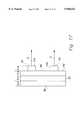
- FIG. 1shows a known structure of a vertical cavity surface emitting laser
- FIGS. 2 and 3show two views of one embodiment of a mode control structure made in accordance with the present invention
- FIGS. 4 and 5show two alternative patterns for the first and second portions of a mode control structure made in accordance with the present invention
- FIG. 6illustrates one principle of a dielectric reflector
- FIG. 7illustrates an alternative reflection reaction at a dielectric reflector
- FIG. 8shows the time-weighted average electric field absolute value in a dielectric stack mirror
- FIG. 9illustrates the absolute value of the time averaged electric field in a full dielectric mirror
- FIG. 10shows the reflectance within a mirror structure as a function of wavelength
- FIG. 11shows the transmittance within a mirror structure as a function of wavelength
- FIGS. 12 and 13show the transmittance as a function of wavelength for two alternative modifications of the mirror represented in FIG. 9;
- FIG. 14represents the reflectance for two regions of a mode control structure having different thicknesses.
- FIGS. 15, 16 and 17represent alternative embodiments of the present invention.
- FIG. 1a cross sectional perspective view of the structure of a typical vertical cavity surface emitting laser is illustrated schematically.
- a metallic contact layer 10is provided with an aperture 12 formed through it.
- the purpose of the aperture 12is to permit the emission of light 14 through the upper surface of the vertical cavity surface emitting laser, or VCSEL.
- a first mirror stack 20below the contact layer is a first mirror stack 20.
- the first mirror stack 20can be selectively damaged by various known techniques, such as ion implantation, to create a region of increased resistance surrounding a central region of lower resistance.
- a top graded index region 24, or upper confinement layer,is provided above a quantum well active region 30.
- a bottom graded index region 32, or lower confinement layer,is disposed below the active region 30.
- the amount of gradingcan vary significantly and the layers can also comprise steps.
- a second mirror stack 34is provided below the lower confinement layer and a substrate 38 is disposed between the lower mirror stack 34 and the contact 22. In a manner well known to those skilled in the art, an electrical current can be caused to flow between the upper contact layer 10 and the lower contact layer 22 to electrically pump the laser and cause the laser to lase.
- the light 14 emitted from the upper surface of the laserwill be of a preselected wavelength.
- the wavelength of light emitted by the laserwill be determined by the materials used to provide the numerous layers within the laser structure and the thickness of the various layers, particularly the first and second mirror stacks.
- the thicknesses of the mirror stack layers, relative to the wavelength of the emitted light,will determine the wavelength of the light 14 emitted from the top layer of the laser.
- the thicknesses of the mirror stack layersare selected as a function of the desired wavelength of emitted light. These thicknesses must be chosen, in the manner that is well known to those skilled in the art, so that the transmittance and reflectance of the layers within the mirror stacks cooperate to cause the laser to lase.
- the dashed boxrepresents the majority of the laser structure shown in FIG. 1. It is identified by reference numeral 41 and should be understood to comprise all of the structures shown in FIG. 1 except the metallic contact 10 and the top layer 21 of the upper mirror structure 20.
- the portions of the laser represented by the dashed lines in FIG. 2are similar to any one of a number of well known laser structures.
- On the top of the upper layer 21 of the mirror structure 20is disposed a mode control structure that comprises first and second portions.
- the first portions 50 of the mode control structureare shaped to permit and encourage the lasing and emission of light through them.
- Second portions 52 of the mode control structureare shaped to inhibit the lasing and emission of light through them.
- the emission of light 14 through the first portions 50 of the mode control structure 60is represented by the arrows in FIG. 2.
- FIG. 3is a top view of FIG. 2 which shows that the first portion 50 of the mode control structure is formed in an annular shape.
- the first portion 50is surrounded by a generally circular second portion 52 of the mode control structure.
- the first portion 50surrounds a generally circular second portion 52 located at the center of the illustration in FIG. 3.
- Surrounding the mode control structureis the nonoverlapping metallic contact 10. Because the preferred lasing region of the laser is formed in the annular shape of the first portion 50 in FIG. 3, the light from the laser can be initially emitted in a radially symmetric shape.
- a lasersuch as that depicted schematically in FIGS. 1, 2 or 3, can be associated with an optical fiber for the transmission of light through the optical fiber in a communication system. The initial emission of light into the fiber would have the radially symmetric shape discussed above.
- FIG. 4shows an alternative arrangement of first and second portions of the mode control structure.
- the first portions 50are arranged in the shapes of five thicker circular patterns with the remaining surface area of the mode control structure being the thinner second portion 52.
- the mode control structure of the laseris configured as shown in FIG. 4, light is initially emitted into the optical fiber as five beams that are radially symmetrical with respect to the center 70 of the mode control structure 60.
- FIG. 5shows another alternative embodiment of the present invention. It comprises eight generally circular first portions 50 arranged in a radially symmetrical pattern with respect to the second portion 52 of the mode control structure 60.
- a laser made in accordance with the configuration of FIG. 5would emit light into the optical fiber as eight individual beams disposed in the pattern shown in FIG. 5.
- the mode control structure of the present inventioncan be shaped in virtually any pattern to determine the relative configurations of the first portions 50 and the second portions 52 of the mode control structure 60. It should also be understood that light is encouraged to lase and is emitted from the thicker first portions 50, but generally inhibited from lasing in the thinner second portions 52 of the mode control structure 60.
- the dielectric interfaceis identified by reference numeral 62.
- the electric fieldis continuous.
- the sum of the fields due to the incident wave 64 and the reflected wave 66equals the transmitted wave 68.
- This principleis illustrated in FIG. 6.
- the index of refractionis greater in the input media, to the left of the dielectric interface 62, than in the output media to the right of the dielectric interface 62.
- the resultis that the reflected wave 62 exhibits no phase reversal relative to the incident wave 64, but is traveling in the negative direction because of the reflection from the dielectric interface 62.
- the reflected wave's phasewould be reversed with respect to the incident wave 64 and it would be traveling in the negative direction.
- a stack of dielectric mirror layerscan be used to make a reflector by designing the thicknesses of the layers so that the reflected waves are additive in phase and do not cancel the incident wave.
- the second interfacewhich does cause a phase reversal, must be displaced by a quarter wavelength so that it is located at the null point of the electric field.
- the third interfacewill then not cause a phase reversal and, therefore, it must be displaced by an integer number of half wavelengths so that the round trip within the laser structure is an integral number of full wavelengths. This is represented in FIG. 7. In FIG.
- reference numeral 74represents the incident wave
- reference numeral 76represents the reflected wave
- reference numeral 78represents the transmitted wave.
- the field on the incident side of the Figure, to the left,is the sum of the reflected and incident waves. They interfere destructively to reduce the intensity of the field.
- reference numeral 64represents the incident electric field
- reference numeral 66represents the reflected electric field
- reference numeral 68represents the transmitted electric field.
- the interfaceis located at a peak in the electric field because the reflected and incident wave electric fields interfere constructively. This is shown, for example, in FIG. 8 at the boundary of layers 140 and 141.
- the peaksappear where there is no phase reversal and the valleys appear where there is a phase reversal because of interference. Reflections come from both surfaces as the light passes through a mirror with minima occurring in the field at the phase reversing interface, making the nonphase reversing interface the dominant reflectance interface. If the interface in FIG. 6 was placed at a quarter wavelength from the interface in FIG. 7 where the position is marked, it should be noted that the reflected waves are in phase and are additive. Therefore, as the light transverses a dielectric stack mirror, a portion of the light is reflected back from each interface. By placing these interfaces a quarter wavelength apart with a period of one half wavelength, the reflected waves all add in phase. In addition, valleys appear at nonphase reversing interfaces and peaks appear at nonface reversing interfaces.
- FIG. 8shows the time-weighted average electric field absolute value in a dielectric stack mirror.
- the incidence of lightis from the right direction in FIG. 8.
- the position of the nullis at the transition from low index of refraction to high index of refraction (i.e. layers 145-144) where a phase reversal occurs.
- the peaksare located at the high index to low index transition (layers 141-140).
- Line 82 in FIG. 8shows the change in the electric field magnitude as a function of position through the thickness of the mirror stack.
- the absolute value of the time averaged electric field in a full dielectric mirror stackcan be seen in FIG. 9.
- the entrance surfaceis located at the right side of FIG. 9.
- the decay, which occurs as the light approaches the left exit surface,is caused because, each time a high-low interface occurs, a small amount of additional light is reflected back with the proper phase.
- the extra two layers on the left side of the structureare lower index dielectric layers that are added to allow the variation of the reflectivity by varying the two additional layers.
- FIG. 10shows the reflectance of the structure described above.
- the magnitude of reflectance, represented by line 102,can be calculated as a function of wavelength.
- the wavelength variation of this structureis caused by the quarterwave stack being optimal for only one wavelength. This is illustrated in FIG. 10.
- FIG. 11shows the transmittance through the ends of the laser. Line 112 represents the transmittance.
- FIG. 12is an enlarged portion of FIG. 11, showing the region between the wavelengths of 840 nanometers and 860 nanometers. Even though this region represents the lowest transmittance for the mirror, it can be seen that some transmission still exists.
- Line 122shows the magnitude of transmittance for the region of FIG. 11 between 840 nanometers and 860 nanometers.
- the results represented in FIG. 12can be modified by changing the layers. For example, if the second layer from the left in FIG. 9 is eliminated, the transmission can be significantly increased. This is represented by line 132 in FIG. 13. In a vertical cavity surface emitting laser, the two layers on the left side of FIG. 9 can easily be patterned to have regions of decreased and increased transmittance.
- FIG. 12 and 13show how the inclusion or elimination of the leftmost layers in FIG. 9 can provide decreased transmittance as represented by line 122 in FIG. 12 or increased transmittance as represented by line 132 in FIG. 13.
- This pattern of the leftmost two layersis used in the preferred embodiment of the present invention to provide first portions of a mode control structure that have increased transmittance, as represented in FIG. 13, and second portions of the mode control structure which have decreased transmittance, as represented by line 122 in FIG. 12.
- FIG. 14represents the reflectance for two regions within a patterned mirror in a vertical cavity surface emitting laser.
- the round trip gainmust equal or exceed the round trip losses for light passing back and fourth between the mirror stacks within the structure of a vertical cavity surface emitting laser. Small changes in reflectance can cause major changes in the gain required for the laser to lase.
- the mirror reflectivitycan be patterned to give regions which cause lasing and regions which inhibit lasing by not having sufficiently high reflectivity.
- the peak reflectance at the top of curve 142is approximately 99.7 percent while the peak reflectance of curve 144 is approximately 98.9 percent.
- the bottom curve 144is therefore 3.7 times as "nonreflective" as the top curve 142. This means that there is 3.7 times as much loss for curve 144 as for curve 142. Therefore, the gain in the active region must be 3.7 times as high, assuming perfect bottom mirrors, in order to achieve laser oscillation with the laser structure.
- the bottom mirrorsare not perfect, but they typically are designed to be much more reflective than the top mirrors in a vertical cavity surface emitting laser. Therefore, the approximation of a perfect bottom mirror is not unacceptable.
- the reflected wavesare additive with the correct phase to increase reflectivity each time a period is added. This can be modified by adding or removing full periods or half periods.
- the reflectivitycan be patterned to create regions within the VCSEL which will lase and others which will not.
- the lasing regionsare referred to herein as the first portions of the mode control structure and the nonlasing regions are referred to herein as the second portions of the mode control structure.
- the filamentation or mode structurecan be controlled.
- etchingthere are numerous possible patterns and several possible methods, such as etching, to accomplish this patterning within the scope of the present invention.
- silicon nitride or silicon dioxideis used on the top surface of the upper mirror and patterned with regions of quarter wavelength and half wavelength thicknesses.
- the half wavelength regions, or first portions of the mode control structurewill lase in a more preferred manner than the quarter wavelength regions, or second portions, of the mode control structure.
- the first portion of the mode control structureis annular in shape, or "doughnut" shaped. This particular embodiment is illustrated in FIGS.
- FIG. 15shows one embodiment of the present invention.
- the mode control structure 60comprises a first portion 50 that is equal to a half wavelength in thickness.
- the second portion 52 of the mode control structure 60is equal to a quarter wavelength. This creates a preferred lasing region through the first portion 50, as represented by arrows L.
- the index of refraction of the components identified by reference numerals 50 and 60must be less than the index of refraction of the component identified by reference numeral 21. In addition, they must be greater than that of the output media which is typically air.
- FIG. 16shows an alternative embodiment of the present invention.
- the mode control structurecomprises a coating 160 over a mode control structure layer 60 that has quarter wavelength regions and half wavelength regions.
- the quarter wavelength regions 50define the preferred regions of lasing for the laser.
- the relationships of the indices of refraction for optimal performanceshould result in component 50 having an index of refraction which is less than that of component 160 but greater than that of the output media.
- the index of refraction of component 21should be greater than the index of refraction of component 50.
- the regions of the surface that do not have component 50 underthen have a quarter wavelength thickness of component 160 over them. This is an antireflection coating that reduces the mirror reflectivity so that laser oscillation is not preferred in this region.
- the regions of the surface where components 50 and 160 both existprovide additional reflectivity to the mirror and enhance laser oscillation.
- FIG. 17shows an alternative embodiment of the present invention which uses multiple patterned dielectric layers.
- a quarter wavelength thick layer of silicon dioxide 172is used for the low reflective region, or second portion 52.
- An additional quarter wavelength layer of silicon nitride 174can be disposed selectively on the surface of layer 172 to create regions of higher reflectivity, or first portions 50 of the mode control structure.
- multiple dielectric patterningis accomplished by using quarter wavelength layers of higher refractive index material to reduce the reflectivity and quarter wavelength layers of higher refractive index material on top of the lower refractive index material for the higher reflectivity regions, or first portions.
- the index of refraction of component 21is greater than the index of refraction of component 174.
- the index of refraction of component 174is greater than that of component 172.
- the index of refraction of component 172is greater than the index of refraction of the output media which is typically air.
- the basic principle of the structure shown in FIG. 17is similar to that of FIG. 16.
- the most desirable of these various alternative structures, if silicon nitride and silicon dioxide are used,is FIG. 16 because the silicon nitride provides a better antireflection coating due to its higher index of refraction than silicon dioxide. However, it should be understood that either structure will work satisfactorily.
- the present inventionprovides a mode control structure for a laser.
- the mode control structurecan comprise two or more thicknesses which are arranged to define a pattern of first portions and second portions of the mode control structure.
- First portionsare provided with a thickness which enhances the lasing of the laser and light is transmitted through the first portions.
- the second portionsare provided with a thickness that inhibits lasing.
- the emission of light from the patterned first portions of the mode control structurecreates a filamentation pattern or modal pattern that is advantageous when the laser is used in signal communication applications.
Landscapes
- Physics & Mathematics (AREA)
- Condensed Matter Physics & Semiconductors (AREA)
- General Physics & Mathematics (AREA)
- Electromagnetism (AREA)
- Optics & Photonics (AREA)
- Semiconductor Lasers (AREA)
Abstract
Description
Claims (29)
Priority Applications (1)
| Application Number | Priority Date | Filing Date | Title |
|---|---|---|---|
| US08/674,230US5940422A (en) | 1996-06-28 | 1996-06-28 | Laser with an improved mode control |
Applications Claiming Priority (1)
| Application Number | Priority Date | Filing Date | Title |
|---|---|---|---|
| US08/674,230US5940422A (en) | 1996-06-28 | 1996-06-28 | Laser with an improved mode control |
Publications (1)
| Publication Number | Publication Date |
|---|---|
| US5940422Atrue US5940422A (en) | 1999-08-17 |
Family
ID=24705833
Family Applications (1)
| Application Number | Title | Priority Date | Filing Date |
|---|---|---|---|
| US08/674,230Expired - LifetimeUS5940422A (en) | 1996-06-28 | 1996-06-28 | Laser with an improved mode control |
Country Status (1)
| Country | Link |
|---|---|
| US (1) | US5940422A (en) |
Cited By (56)
| Publication number | Priority date | Publication date | Assignee | Title |
|---|---|---|---|---|
| WO2001095443A1 (en)* | 1999-06-02 | 2001-12-13 | Cielo Communications, Inc. | Single mode vertical cavity surface emitting laser |
| US20020085610A1 (en)* | 2000-12-29 | 2002-07-04 | Morgan Robert A. | Spatially modulated reflector for an optoelectronic device |
| US20020106160A1 (en)* | 2000-12-29 | 2002-08-08 | Honeywell International Inc. | Resonant reflector for increased wavelength and polarization control |
| JP2002359432A (en)* | 2001-03-27 | 2002-12-13 | Fuji Xerox Co Ltd | Surface emission type semiconductor laser and method for manufacturing the same |
| US6534331B2 (en) | 2001-07-24 | 2003-03-18 | Luxnet Corporation | Method for making a vertical-cavity surface emitting laser with improved current confinement |
| GB2379797A (en)* | 2001-09-15 | 2003-03-19 | Zarlink Semiconductor Ab | Surface Emitting Laser |
| US6553053B2 (en)* | 2001-07-25 | 2003-04-22 | Luxnet Corporation | Vertical cavity surface emitting laser having improved light output function |
| US6556329B1 (en)* | 1998-05-21 | 2003-04-29 | Enterasys Networks, Inc. | Method and system for preventing low order optical transmission modes in multimode optical fiber computer network using annulus laser |
| US6590917B2 (en)* | 1998-07-06 | 2003-07-08 | Fuji Xerox Co., Ltd. | Surface emitting laser and surface emitting laser array |
| US6606199B2 (en) | 2001-10-10 | 2003-08-12 | Honeywell International Inc. | Graded thickness optical element and method of manufacture therefor |
| US6680963B2 (en) | 2001-07-24 | 2004-01-20 | Lux Net Corporation | Vertical-cavity surface emitting laser utilizing a reversed biased diode for improved current confinement |
| US20040081215A1 (en)* | 2002-10-28 | 2004-04-29 | Honeywell International Inc. | Distributed bragg reflector for optoelectronic device |
| US20040101009A1 (en)* | 2002-11-21 | 2004-05-27 | Honeywell International Inc. | Long wavelength VCSEL with tunnel junction, and implant |
| US6751245B1 (en) | 1999-06-02 | 2004-06-15 | Optical Communication Products, Inc. | Single mode vertical cavity surface emitting laser |
| US6782027B2 (en) | 2000-12-29 | 2004-08-24 | Finisar Corporation | Resonant reflector for use with optoelectronic devices |
| US20040213311A1 (en)* | 2000-11-28 | 2004-10-28 | Johnson Ralph H | Single mode vertical cavity surface emitting laser |
| US6816527B2 (en) | 2002-07-29 | 2004-11-09 | Fuji Xerox Co., Ltd. | Surface emitting semiconductor laser |
| US6816531B1 (en) | 2000-03-03 | 2004-11-09 | Jds Uniphase Corporation | High-power, kink-free, single mode laser diodes |
| US20040222363A1 (en)* | 2003-05-07 | 2004-11-11 | Honeywell International Inc. | Connectorized optical component misalignment detection system |
| FR2855661A1 (en)* | 2003-05-26 | 2004-12-03 | Optogone Sa | VERTICAL CAVITY AND SURFACE EMISSION LASER, TELECOMMUNICATION SYSTEM AND METHOD THEREOF |
| US20040247250A1 (en)* | 2003-06-03 | 2004-12-09 | Honeywell International Inc. | Integrated sleeve pluggable package |
| US20040264536A1 (en)* | 2003-06-27 | 2004-12-30 | Honeywell International Inc. | Dielectric VCSEL gain guide |
| US20040264530A1 (en)* | 2003-06-27 | 2004-12-30 | Honeywell International Inc. | VCSEL having thermal management |
| US20050013539A1 (en)* | 2003-07-17 | 2005-01-20 | Honeywell International Inc. | Optical coupling system |
| US20050013542A1 (en)* | 2003-07-16 | 2005-01-20 | Honeywell International Inc. | Coupler having reduction of reflections to light source |
| US20050014390A1 (en)* | 2003-07-18 | 2005-01-20 | Honeywell International Inc. | Edge bead control method and apparatus |
| US20050031011A1 (en)* | 2000-11-28 | 2005-02-10 | Biard James R. | Electron affinity engineered VCSELs |
| US20050036533A1 (en)* | 2000-12-29 | 2005-02-17 | Honeywell To Finisar | Tunable detector |
| KR100475858B1 (en)* | 2002-04-01 | 2005-03-18 | 주식회사 테라스테이트 | A Vertical Cavity Surface Emitting Lasers |
| US20050092710A1 (en)* | 2003-10-29 | 2005-05-05 | Biard James R. | Long wavelength VCSEL device processing |
| US6961489B2 (en) | 2003-06-30 | 2005-11-01 | Finisar Corporation | High speed optical system |
| US6965626B2 (en) | 2002-09-03 | 2005-11-15 | Finisar Corporation | Single mode VCSEL |
| US20060029118A1 (en)* | 2004-08-03 | 2006-02-09 | Chih-Cheng Chen | High-power single-mode vertical cavity-surface emitting laser |
| US20060045146A1 (en)* | 2004-08-31 | 2006-03-02 | Finisar Corporation | Mode selective semiconductor mirror for vertical cavity surface emitting lasers |
| US20060045162A1 (en)* | 2004-08-31 | 2006-03-02 | Finisar Corporation | Distributed bragg reflector for optoelectronic device |
| US20060056762A1 (en)* | 2003-07-02 | 2006-03-16 | Honeywell International Inc. | Lens optical coupler |
| US7054345B2 (en) | 2003-06-27 | 2006-05-30 | Finisar Corporation | Enhanced lateral oxidation |
| US20060187987A1 (en)* | 2005-02-18 | 2006-08-24 | Opnext Japan, Inc. | Semiconductor laser diode |
| US7149383B2 (en) | 2003-06-30 | 2006-12-12 | Finisar Corporation | Optical system with reduced back reflection |
| US7210857B2 (en) | 2003-07-16 | 2007-05-01 | Finisar Corporation | Optical coupling system |
| US20070217472A1 (en)* | 2006-03-14 | 2007-09-20 | Doug Collins | VCSEL semiconductor devices with mode control |
| US7298942B2 (en) | 2003-06-06 | 2007-11-20 | Finisar Corporation | Pluggable optical optic system having a lens fiber stop |
| US20080023688A1 (en)* | 2006-07-31 | 2008-01-31 | Finisar Corporation | Efficient carrier injection in a semiconductor device |
| US7433381B2 (en) | 2003-06-25 | 2008-10-07 | Finisar Corporation | InP based long wavelength VCSEL |
| US20090155944A1 (en)* | 2004-10-13 | 2009-06-18 | Naoto Jikutani | Surface Emitting Laser Device and Production Method |
| US7920612B2 (en) | 2004-08-31 | 2011-04-05 | Finisar Corporation | Light emitting semiconductor device having an electrical confinement barrier near the active region |
| WO2011021139A3 (en)* | 2009-08-20 | 2011-05-05 | Koninklijke Philips Electronics N.V. | A vertical cavity surface emitting laser device with angular-selective feedback |
| EP2323231A1 (en)* | 2009-11-17 | 2011-05-18 | Ricoh Company, Ltd. | Surface-emitting laser element, surface-emitting laser array, optical scanner device, and image forming apparatus |
| US20110116147A1 (en)* | 2009-11-18 | 2011-05-19 | Ricoh Company, Ltd. | Surface emitting laser device, surface emitting laser array, optical scanning device, and image forming apparatus |
| EP2328244A1 (en) | 2009-11-27 | 2011-06-01 | Ricoh Company, Ltd. | Surface-emitting laser element, surface-emitting laser array, optical scanner device, and image forming apparatus |
| US8031752B1 (en) | 2007-04-16 | 2011-10-04 | Finisar Corporation | VCSEL optimized for high speed data |
| US8189642B1 (en) | 2007-08-08 | 2012-05-29 | Emcore Corporation | VCSEL semiconductor device |
| US20130234108A1 (en)* | 2012-03-06 | 2013-09-12 | Soraa, Inc. | Light emitting diodes with low refractive index material layers to reduce light guiding effects |
| DE112006003384B4 (en) | 2005-12-12 | 2014-01-02 | Finisar Corp. | Surface grid on VCSELs for polarization pinning |
| JP2014027011A (en)* | 2012-07-24 | 2014-02-06 | Nippon Hoso Kyokai <Nhk> | Light-emitting element |
| WO2019171003A1 (en)* | 2018-03-08 | 2019-09-12 | Commissariat à l'énergie atomique et aux énergies alternatives | Light emission device comprising at least one vcsel and a spread lens |
Citations (17)
| Publication number | Priority date | Publication date | Assignee | Title |
|---|---|---|---|---|
| US4749255A (en)* | 1985-12-09 | 1988-06-07 | American Telephone And Telegraph Company, At&T Bell Laboratories | Coating for optical devices |
| JPH0194689A (en)* | 1987-10-06 | 1989-04-13 | Furukawa Electric Co Ltd:The | optical semiconductor device |
| US5031187A (en)* | 1990-02-14 | 1991-07-09 | Bell Communications Research, Inc. | Planar array of vertical-cavity, surface-emitting lasers |
| US5052016A (en)* | 1990-05-18 | 1991-09-24 | University Of New Mexico | Resonant-periodic-gain distributed-feedback surface-emitting semiconductor laser |
| US5115442A (en)* | 1990-04-13 | 1992-05-19 | At&T Bell Laboratories | Top-emitting surface emitting laser structures |
| US5164949A (en)* | 1991-09-09 | 1992-11-17 | Motorola, Inc. | Vertical cavity surface emitting laser with lateral injection |
| US5237581A (en)* | 1990-11-14 | 1993-08-17 | Nec Corporation | Semiconductor multilayer reflector and light emitting device with the same |
| US5245622A (en)* | 1992-05-07 | 1993-09-14 | Bandgap Technology Corporation | Vertical-cavity surface-emitting lasers with intra-cavity structures |
| US5258990A (en)* | 1991-11-07 | 1993-11-02 | The United States Of America As Represented By The Secretary Of The United States Department Of Energy | Visible light surface emitting semiconductor laser |
| US5331654A (en)* | 1993-03-05 | 1994-07-19 | Photonics Research Incorporated | Polarized surface-emitting laser |
| US5351256A (en)* | 1993-04-28 | 1994-09-27 | The United States Of America As Represented By The United States Department Of Energy | Electrically injected visible vertical cavity surface emitting laser diodes |
| US5359447A (en)* | 1993-06-25 | 1994-10-25 | Hewlett-Packard Company | Optical communication with vertical-cavity surface-emitting laser operating in multiple transverse modes |
| US5493577A (en)* | 1994-12-21 | 1996-02-20 | Sandia Corporation | Efficient semiconductor light-emitting device and method |
| US5492607A (en)* | 1993-02-17 | 1996-02-20 | Hughes Aircraft Company | Method of fabricating a surface emitting laser with large area deflecting mirror |
| US5537666A (en)* | 1990-09-12 | 1996-07-16 | Seiko Epson Coropration | Surface emission type semiconductor laser |
| US5557627A (en)* | 1995-05-19 | 1996-09-17 | Sandia Corporation | Visible-wavelength semiconductor lasers and arrays |
| US5574738A (en)* | 1995-06-07 | 1996-11-12 | Honeywell Inc. | Multi-gigahertz frequency-modulated vertical-cavity surface emitting laser |
- 1996
- 1996-06-28USUS08/674,230patent/US5940422A/ennot_activeExpired - Lifetime
Patent Citations (17)
| Publication number | Priority date | Publication date | Assignee | Title |
|---|---|---|---|---|
| US4749255A (en)* | 1985-12-09 | 1988-06-07 | American Telephone And Telegraph Company, At&T Bell Laboratories | Coating for optical devices |
| JPH0194689A (en)* | 1987-10-06 | 1989-04-13 | Furukawa Electric Co Ltd:The | optical semiconductor device |
| US5031187A (en)* | 1990-02-14 | 1991-07-09 | Bell Communications Research, Inc. | Planar array of vertical-cavity, surface-emitting lasers |
| US5115442A (en)* | 1990-04-13 | 1992-05-19 | At&T Bell Laboratories | Top-emitting surface emitting laser structures |
| US5052016A (en)* | 1990-05-18 | 1991-09-24 | University Of New Mexico | Resonant-periodic-gain distributed-feedback surface-emitting semiconductor laser |
| US5537666A (en)* | 1990-09-12 | 1996-07-16 | Seiko Epson Coropration | Surface emission type semiconductor laser |
| US5237581A (en)* | 1990-11-14 | 1993-08-17 | Nec Corporation | Semiconductor multilayer reflector and light emitting device with the same |
| US5164949A (en)* | 1991-09-09 | 1992-11-17 | Motorola, Inc. | Vertical cavity surface emitting laser with lateral injection |
| US5258990A (en)* | 1991-11-07 | 1993-11-02 | The United States Of America As Represented By The Secretary Of The United States Department Of Energy | Visible light surface emitting semiconductor laser |
| US5245622A (en)* | 1992-05-07 | 1993-09-14 | Bandgap Technology Corporation | Vertical-cavity surface-emitting lasers with intra-cavity structures |
| US5492607A (en)* | 1993-02-17 | 1996-02-20 | Hughes Aircraft Company | Method of fabricating a surface emitting laser with large area deflecting mirror |
| US5331654A (en)* | 1993-03-05 | 1994-07-19 | Photonics Research Incorporated | Polarized surface-emitting laser |
| US5351256A (en)* | 1993-04-28 | 1994-09-27 | The United States Of America As Represented By The United States Department Of Energy | Electrically injected visible vertical cavity surface emitting laser diodes |
| US5359447A (en)* | 1993-06-25 | 1994-10-25 | Hewlett-Packard Company | Optical communication with vertical-cavity surface-emitting laser operating in multiple transverse modes |
| US5493577A (en)* | 1994-12-21 | 1996-02-20 | Sandia Corporation | Efficient semiconductor light-emitting device and method |
| US5557627A (en)* | 1995-05-19 | 1996-09-17 | Sandia Corporation | Visible-wavelength semiconductor lasers and arrays |
| US5574738A (en)* | 1995-06-07 | 1996-11-12 | Honeywell Inc. | Multi-gigahertz frequency-modulated vertical-cavity surface emitting laser |
Non-Patent Citations (5)
| Title |
|---|
| Article titled 200 °C, 96-nm Wavelength Range, Continuous-Wave Lasing from Unbonded GAAS MOUPE-Grown Vertical Surface Emitting Laser by Morgan et al., Oct. 1995. |
| Article titled 200 C, 96 nm Wavelength Range, Continuous Wave Lasing from Unbonded GAAS MOUPE Grown Vertical Surface Emitting Laser by Morgan et al., Oct. 1995.* |
| Article Titled Services for Optical Processing by Morgan et al., Jul. 1991.* |
| Article Titled Surface Emitting Microlasers for Photonic Switching and Interchip Connections by Jewell et al., Mar. 1990.* |
| Article titled Transverse Mode Control of Vertical Cavity Top Surface. Emitting Lasers by Morgan et al., Apr. 1993.* |
Cited By (106)
| Publication number | Priority date | Publication date | Assignee | Title |
|---|---|---|---|---|
| US6556329B1 (en)* | 1998-05-21 | 2003-04-29 | Enterasys Networks, Inc. | Method and system for preventing low order optical transmission modes in multimode optical fiber computer network using annulus laser |
| US6590917B2 (en)* | 1998-07-06 | 2003-07-08 | Fuji Xerox Co., Ltd. | Surface emitting laser and surface emitting laser array |
| WO2001095443A1 (en)* | 1999-06-02 | 2001-12-13 | Cielo Communications, Inc. | Single mode vertical cavity surface emitting laser |
| US6751245B1 (en) | 1999-06-02 | 2004-06-15 | Optical Communication Products, Inc. | Single mode vertical cavity surface emitting laser |
| US6816531B1 (en) | 2000-03-03 | 2004-11-09 | Jds Uniphase Corporation | High-power, kink-free, single mode laser diodes |
| US7221691B2 (en) | 2000-11-28 | 2007-05-22 | Finisar Corporation | Versatile method and system for single mode VCSELs |
| US20040213311A1 (en)* | 2000-11-28 | 2004-10-28 | Johnson Ralph H | Single mode vertical cavity surface emitting laser |
| US6905900B1 (en) | 2000-11-28 | 2005-06-14 | Finisar Corporation | Versatile method and system for single mode VCSELs |
| US7065124B2 (en) | 2000-11-28 | 2006-06-20 | Finlsar Corporation | Electron affinity engineered VCSELs |
| US7308011B2 (en) | 2000-11-28 | 2007-12-11 | Finisar Corporation | Versatile method and system for single mode VCSELs |
| US20050031011A1 (en)* | 2000-11-28 | 2005-02-10 | Biard James R. | Electron affinity engineered VCSELs |
| US20050036533A1 (en)* | 2000-12-29 | 2005-02-17 | Honeywell To Finisar | Tunable detector |
| WO2002059938A3 (en)* | 2000-12-29 | 2003-07-31 | Honeywell Int Inc | Spatially modulated reflector for an optoelectronic device |
| US6727520B2 (en)* | 2000-12-29 | 2004-04-27 | Honeywell International Inc. | Spatially modulated reflector for an optoelectronic device |
| US6836501B2 (en) | 2000-12-29 | 2004-12-28 | Finisar Corporation | Resonant reflector for increased wavelength and polarization control |
| US8599897B2 (en) | 2000-12-29 | 2013-12-03 | Finisar Corporation | Tunable detector |
| US7760786B2 (en) | 2000-12-29 | 2010-07-20 | Finisar Corporation | Laser with resonant reflector |
| US6782027B2 (en) | 2000-12-29 | 2004-08-24 | Finisar Corporation | Resonant reflector for use with optoelectronic devices |
| US20040188695A1 (en)* | 2000-12-29 | 2004-09-30 | Morgan Robert A. | Laser with resonant reflector |
| US20040191941A1 (en)* | 2000-12-29 | 2004-09-30 | Morgan Robert A. | Method for producing laser with resonant reflector |
| US20020106160A1 (en)* | 2000-12-29 | 2002-08-08 | Honeywell International Inc. | Resonant reflector for increased wavelength and polarization control |
| US7266135B2 (en) | 2000-12-29 | 2007-09-04 | Finisar Corporation | Method for producing laser with resonant reflector |
| US20020085610A1 (en)* | 2000-12-29 | 2002-07-04 | Morgan Robert A. | Spatially modulated reflector for an optoelectronic device |
| US7288421B2 (en) | 2000-12-29 | 2007-10-30 | Finisar Corporation | Method for forming an optoelectronic device having an isolation layer |
| US6990128B2 (en) | 2001-03-27 | 2006-01-24 | Fuji Xerox Co., Ltd. | Surface emitting semiconductor laser and manufacturing method thereof |
| US20040219699A1 (en)* | 2001-03-27 | 2004-11-04 | Fuji Xerox Co., Ltd. | Surface emitting semiconductor laser and manufacturing method thereof |
| US7141441B2 (en) | 2001-03-27 | 2006-11-28 | Fuji Xerox Co., Ltd. | Surface emitting semiconductor laser and manufacturing method thereof |
| JP2002359432A (en)* | 2001-03-27 | 2002-12-13 | Fuji Xerox Co Ltd | Surface emission type semiconductor laser and method for manufacturing the same |
| US6680963B2 (en) | 2001-07-24 | 2004-01-20 | Lux Net Corporation | Vertical-cavity surface emitting laser utilizing a reversed biased diode for improved current confinement |
| US6534331B2 (en) | 2001-07-24 | 2003-03-18 | Luxnet Corporation | Method for making a vertical-cavity surface emitting laser with improved current confinement |
| US6553053B2 (en)* | 2001-07-25 | 2003-04-22 | Luxnet Corporation | Vertical cavity surface emitting laser having improved light output function |
| US6885690B2 (en) | 2001-09-15 | 2005-04-26 | Zarlink Semiconductor Ab | Transverse mode and polarization control of surface emitting lasers through the formation of a dielectric stack |
| GB2379797A (en)* | 2001-09-15 | 2003-03-19 | Zarlink Semiconductor Ab | Surface Emitting Laser |
| US20030063642A1 (en)* | 2001-09-15 | 2003-04-03 | Zarlink Semiconductor Ab | Transverse mode and polarization control of surface emitting lasers through the formation of a dielectric stack |
| US6606199B2 (en) | 2001-10-10 | 2003-08-12 | Honeywell International Inc. | Graded thickness optical element and method of manufacture therefor |
| KR100475858B1 (en)* | 2002-04-01 | 2005-03-18 | 주식회사 테라스테이트 | A Vertical Cavity Surface Emitting Lasers |
| US6816527B2 (en) | 2002-07-29 | 2004-11-09 | Fuji Xerox Co., Ltd. | Surface emitting semiconductor laser |
| US6965626B2 (en) | 2002-09-03 | 2005-11-15 | Finisar Corporation | Single mode VCSEL |
| US7251264B2 (en) | 2002-10-28 | 2007-07-31 | Finisar Corporation | Distributed bragg reflector for optoelectronic device |
| US6990135B2 (en) | 2002-10-28 | 2006-01-24 | Finisar Corporation | Distributed bragg reflector for optoelectronic device |
| US20040081215A1 (en)* | 2002-10-28 | 2004-04-29 | Honeywell International Inc. | Distributed bragg reflector for optoelectronic device |
| US20050190812A1 (en)* | 2002-10-28 | 2005-09-01 | Johnson Ralph H. | Distributed bragg reflector for optoelectronic device |
| US20040101009A1 (en)* | 2002-11-21 | 2004-05-27 | Honeywell International Inc. | Long wavelength VCSEL with tunnel junction, and implant |
| US6813293B2 (en) | 2002-11-21 | 2004-11-02 | Finisar Corporation | Long wavelength VCSEL with tunnel junction, and implant |
| US20040222363A1 (en)* | 2003-05-07 | 2004-11-11 | Honeywell International Inc. | Connectorized optical component misalignment detection system |
| US20050281297A1 (en)* | 2003-05-26 | 2005-12-22 | Optogone | Vertical cavity surface emitting laser, telecommunication system and corresponding method |
| FR2855661A1 (en)* | 2003-05-26 | 2004-12-03 | Optogone Sa | VERTICAL CAVITY AND SURFACE EMISSION LASER, TELECOMMUNICATION SYSTEM AND METHOD THEREOF |
| US20040247250A1 (en)* | 2003-06-03 | 2004-12-09 | Honeywell International Inc. | Integrated sleeve pluggable package |
| US7298942B2 (en) | 2003-06-06 | 2007-11-20 | Finisar Corporation | Pluggable optical optic system having a lens fiber stop |
| US7433381B2 (en) | 2003-06-25 | 2008-10-07 | Finisar Corporation | InP based long wavelength VCSEL |
| US7054345B2 (en) | 2003-06-27 | 2006-05-30 | Finisar Corporation | Enhanced lateral oxidation |
| US20040264530A1 (en)* | 2003-06-27 | 2004-12-30 | Honeywell International Inc. | VCSEL having thermal management |
| US7075962B2 (en) | 2003-06-27 | 2006-07-11 | Finisar Corporation | VCSEL having thermal management |
| US20040264536A1 (en)* | 2003-06-27 | 2004-12-30 | Honeywell International Inc. | Dielectric VCSEL gain guide |
| US7277461B2 (en) | 2003-06-27 | 2007-10-02 | Finisar Corporation | Dielectric VCSEL gain guide |
| US6961489B2 (en) | 2003-06-30 | 2005-11-01 | Finisar Corporation | High speed optical system |
| US7139454B2 (en) | 2003-06-30 | 2006-11-21 | Finisar Corporation | Methods for signal transmission in optical fiber |
| US7149383B2 (en) | 2003-06-30 | 2006-12-12 | Finisar Corporation | Optical system with reduced back reflection |
| US20060056762A1 (en)* | 2003-07-02 | 2006-03-16 | Honeywell International Inc. | Lens optical coupler |
| US7210857B2 (en) | 2003-07-16 | 2007-05-01 | Finisar Corporation | Optical coupling system |
| US20050013542A1 (en)* | 2003-07-16 | 2005-01-20 | Honeywell International Inc. | Coupler having reduction of reflections to light source |
| US20050013539A1 (en)* | 2003-07-17 | 2005-01-20 | Honeywell International Inc. | Optical coupling system |
| US6887801B2 (en) | 2003-07-18 | 2005-05-03 | Finisar Corporation | Edge bead control method and apparatus |
| US20050014390A1 (en)* | 2003-07-18 | 2005-01-20 | Honeywell International Inc. | Edge bead control method and apparatus |
| US20050092710A1 (en)* | 2003-10-29 | 2005-05-05 | Biard James R. | Long wavelength VCSEL device processing |
| US7031363B2 (en) | 2003-10-29 | 2006-04-18 | Finisar Corporation | Long wavelength VCSEL device processing |
| US20060029118A1 (en)* | 2004-08-03 | 2006-02-09 | Chih-Cheng Chen | High-power single-mode vertical cavity-surface emitting laser |
| US7920612B2 (en) | 2004-08-31 | 2011-04-05 | Finisar Corporation | Light emitting semiconductor device having an electrical confinement barrier near the active region |
| US7596165B2 (en) | 2004-08-31 | 2009-09-29 | Finisar Corporation | Distributed Bragg Reflector for optoelectronic device |
| WO2006026644A3 (en)* | 2004-08-31 | 2007-05-03 | Finisar Corp | Mode selective semiconductor mirror for vertical cavity surface emitting lasers |
| US7391799B2 (en)* | 2004-08-31 | 2008-06-24 | Finisar Corporation | Mode selective semiconductor mirror for vertical cavity surface emitting lasers |
| US20060045146A1 (en)* | 2004-08-31 | 2006-03-02 | Finisar Corporation | Mode selective semiconductor mirror for vertical cavity surface emitting lasers |
| US20060045162A1 (en)* | 2004-08-31 | 2006-03-02 | Finisar Corporation | Distributed bragg reflector for optoelectronic device |
| US7760787B2 (en)* | 2004-10-13 | 2010-07-20 | Ricoh Company, Ltd. | Surface emitting laser device and production method |
| US20090155944A1 (en)* | 2004-10-13 | 2009-06-18 | Naoto Jikutani | Surface Emitting Laser Device and Production Method |
| US7542498B2 (en)* | 2005-02-18 | 2009-06-02 | Opnext Japan, Inc. | Semiconductor laser diode |
| US20060187987A1 (en)* | 2005-02-18 | 2006-08-24 | Opnext Japan, Inc. | Semiconductor laser diode |
| DE112006003384B4 (en) | 2005-12-12 | 2014-01-02 | Finisar Corp. | Surface grid on VCSELs for polarization pinning |
| US20070217472A1 (en)* | 2006-03-14 | 2007-09-20 | Doug Collins | VCSEL semiconductor devices with mode control |
| US20080023688A1 (en)* | 2006-07-31 | 2008-01-31 | Finisar Corporation | Efficient carrier injection in a semiconductor device |
| US7829912B2 (en) | 2006-07-31 | 2010-11-09 | Finisar Corporation | Efficient carrier injection in a semiconductor device |
| US8031752B1 (en) | 2007-04-16 | 2011-10-04 | Finisar Corporation | VCSEL optimized for high speed data |
| US8189642B1 (en) | 2007-08-08 | 2012-05-29 | Emcore Corporation | VCSEL semiconductor device |
| WO2011021139A3 (en)* | 2009-08-20 | 2011-05-05 | Koninklijke Philips Electronics N.V. | A vertical cavity surface emitting laser device with angular-selective feedback |
| US9153941B2 (en) | 2009-08-20 | 2015-10-06 | Koninklijke Philips N.V. | Vertical cavity surface emitting laser device with angular-selective feedback |
| JP2013502716A (en)* | 2009-08-20 | 2013-01-24 | コーニンクレッカ フィリップス エレクトロニクス エヌ ヴィ | Vertical cavity surface emitting laser device with angle selective feedback |
| US8441511B2 (en)* | 2009-11-17 | 2013-05-14 | Ricoh Company, Ltd. | Surface-emitting laser element including dielectric film selectively provided to control reflectance in emission region, surface-emitting laser array, optical scanner device, and image forming apparatus |
| US20110115872A1 (en)* | 2009-11-17 | 2011-05-19 | Ricoh Company, Ltd. | Surface-emitting laser element, surface-emitting laser array, optical scanner device, and image forming apparatus |
| EP2323231A1 (en)* | 2009-11-17 | 2011-05-18 | Ricoh Company, Ltd. | Surface-emitting laser element, surface-emitting laser array, optical scanner device, and image forming apparatus |
| EP2325957A2 (en) | 2009-11-18 | 2011-05-25 | Ricoh Company Ltd. | Surface emitting laser device, surface emitting laser array, optical scanning device, and image forming apparatus |
| US20110116147A1 (en)* | 2009-11-18 | 2011-05-19 | Ricoh Company, Ltd. | Surface emitting laser device, surface emitting laser array, optical scanning device, and image forming apparatus |
| US8711891B2 (en) | 2009-11-18 | 2014-04-29 | Ricoh Company, Ltd. | Surface emitting laser device, surface emitting laser array, optical scanning device, and image forming apparatus |
| US20110128343A1 (en)* | 2009-11-27 | 2011-06-02 | Ricoh Company, Ltd. | Surface-emitting laser element, surface-emitting laser array, optical scanner device, and image forming apparatus |
| EP2328244A1 (en) | 2009-11-27 | 2011-06-01 | Ricoh Company, Ltd. | Surface-emitting laser element, surface-emitting laser array, optical scanner device, and image forming apparatus |
| US8855159B2 (en) | 2009-11-27 | 2014-10-07 | Ricoh Company, Ltd. | Surface-emitting laser element, surface-emitting laser array, optical scanner device, and image forming apparatus |
| US20130234108A1 (en)* | 2012-03-06 | 2013-09-12 | Soraa, Inc. | Light emitting diodes with low refractive index material layers to reduce light guiding effects |
| US9269876B2 (en)* | 2012-03-06 | 2016-02-23 | Soraa, Inc. | Light emitting diodes with low refractive index material layers to reduce light guiding effects |
| US20160172556A1 (en)* | 2012-03-06 | 2016-06-16 | Soraa, Inc. | Light emitting diode with low refractive index material layers to reduce light guiding effects |
| US10096755B2 (en)* | 2012-03-06 | 2018-10-09 | Soraa, Inc. | Light emitting diode with low refractive index material layers to reduce light guiding effects |
| US20190140150A1 (en)* | 2012-03-06 | 2019-05-09 | Soraa, Inc. | Light emitting diode with low refractive index material layers to reduce light guiding effects |
| JP2014027011A (en)* | 2012-07-24 | 2014-02-06 | Nippon Hoso Kyokai <Nhk> | Light-emitting element |
| WO2019171003A1 (en)* | 2018-03-08 | 2019-09-12 | Commissariat à l'énergie atomique et aux énergies alternatives | Light emission device comprising at least one vcsel and a spread lens |
| FR3078834A1 (en)* | 2018-03-08 | 2019-09-13 | Commissariat A L'energie Atomique Et Aux Energies Alternatives | LIGHT EMITTING DEVICE COMPRISING AT LEAST ONE VCSEL AND A DIFFUSION LENS |
| CN111837301A (en)* | 2018-03-08 | 2020-10-27 | 原子能和替代能源委员会 | Light emitting device including at least one VCSEL and diffuser lens |
| US11418009B2 (en) | 2018-03-08 | 2022-08-16 | Commissariat A L'energie Atomique Et Aux Energies Alternatives | Light emission device comprising at least one VCSEL and a spread lens |
| CN111837301B (en)* | 2018-03-08 | 2024-03-01 | 原子能和替代能源委员会 | Light emitting device comprising at least one VCSEL and a diffusion lens |
Similar Documents
| Publication | Publication Date | Title |
|---|---|---|
| US5940422A (en) | Laser with an improved mode control | |
| US6154480A (en) | Vertical-cavity laser and laser array incorporating guided-mode resonance effects and method for making the same | |
| US7288421B2 (en) | Method for forming an optoelectronic device having an isolation layer | |
| US4873696A (en) | Surface-emitting lasers with periodic gain and a parallel driven nipi structure | |
| US5745515A (en) | Self-limiting intrinsically eye-safe laser utilizing an increasing absorption layer | |
| EP1208622B1 (en) | Coupled cavity anti-guided vertical cavity surface emitting laser (vcsel) | |
| US5799030A (en) | Semiconductor device with a laser and a photodetector in a common container | |
| US6026111A (en) | Vertical cavity surface emitting laser device having an extended cavity | |
| CA2478174C (en) | Mode control using transversal bandgap structure in vcsels | |
| US6055262A (en) | Resonant reflector for improved optoelectronic device performance and enhanced applicability | |
| JP4621393B2 (en) | Surface emitting semiconductor laser and method for manufacturing surface emitting semiconductor laser | |
| US6259121B1 (en) | Monolithic multiple wavelength VCSEL array | |
| US5812581A (en) | Lens for a semiconductive device with a laser and a photodetector in a common container | |
| KR20010079633A (en) | Injection laser | |
| JP2004063707A (en) | Surface emitting type semiconductor laser | |
| WO1992010867A1 (en) | Phase-locked array of reflectivity-modulated surface-emitting lasers | |
| US5052008A (en) | Current injection laser | |
| US6021146A (en) | Vertical cavity surface emitting laser for high power single mode operation and method of fabrication | |
| JPH05299689A (en) | Surface input / output optoelectronic device | |
| US4894833A (en) | Surface emitting lasers with combined output | |
| US7292613B2 (en) | Half-wavelength micropost microcavity with electric field maximum in the high-refractive-index material | |
| WO2025118764A1 (en) | Antireflective vertical-cavity surface-emitting laser and chip | |
| US5539759A (en) | Single mode laser with a passive antiguide region | |
| WO2004064211A1 (en) | Laser array | |
| US8693894B2 (en) | Gain clamped optical device for emitting LED mode light |
Legal Events
| Date | Code | Title | Description |
|---|---|---|---|
| AS | Assignment | Owner name:HONEYWELL INC., MINNESOTA Free format text:ASSIGNMENT OF ASSIGNORS INTEREST;ASSIGNOR:JOHNSON, RALPH H.;REEL/FRAME:008091/0907 Effective date:19960626 | |
| STCF | Information on status: patent grant | Free format text:PATENTED CASE | |
| FEPP | Fee payment procedure | Free format text:PAYOR NUMBER ASSIGNED (ORIGINAL EVENT CODE: ASPN); ENTITY STATUS OF PATENT OWNER: LARGE ENTITY | |
| FPAY | Fee payment | Year of fee payment:4 | |
| AS | Assignment | Owner name:FINISAR CORPORATION, CALIFORNIA Free format text:ASSIGNMENT OF ASSIGNORS INTEREST;ASSIGNOR:HONEYWELL INTERNATIONAL, INC.;REEL/FRAME:014468/0371 Effective date:20040301 Owner name:FINISAR CORPORATION, CALIFORNIA Free format text:ASSIGNMENT OF ASSIGNORS INTEREST;ASSIGNOR:HONEYWELL INTERNATIONAL, INC.;REEL/FRAME:014468/0407 Effective date:20040301 Owner name:FINISAR CORPORATION, CALIFORNIA Free format text:ASSIGNMENT OF ASSIGNORS INTEREST;ASSIGNOR:HONEYWELL INTERNATIONAL, INC.;REEL/FRAME:014484/0171 Effective date:20040301 | |
| AS | Assignment | Owner name:FINISAR CORPORATION, CALIFORNIA Free format text:ASSIGNMENT OF ASSIGNORS INTEREST;ASSIGNOR:HONEYWELL INTERNATIONAL, INC.;REEL/FRAME:014499/0365 Effective date:20040301 | |
| FPAY | Fee payment | Year of fee payment:8 | |
| FPAY | Fee payment | Year of fee payment:12 | |
| AS | Assignment | Owner name:II-VI DELAWARE, INC., DELAWARE Free format text:ASSIGNMENT OF ASSIGNORS INTEREST;ASSIGNOR:FINISAR CORPORATION;REEL/FRAME:052286/0001 Effective date:20190924 |