US5940362A - Disc device having a magnetic layer overweighing the information signal pattern for electronic article surveillance - Google Patents
Disc device having a magnetic layer overweighing the information signal pattern for electronic article surveillanceDownload PDFInfo
- Publication number
- US5940362A US5940362AUS08/699,494US69949496AUS5940362AUS 5940362 AUS5940362 AUS 5940362AUS 69949496 AUS69949496 AUS 69949496AUS 5940362 AUS5940362 AUS 5940362A
- Authority
- US
- United States
- Prior art keywords
- material layer
- layer
- disc
- magnetic material
- signal pattern
- Prior art date
- Legal status (The legal status is an assumption and is not a legal conclusion. Google has not performed a legal analysis and makes no representation as to the accuracy of the status listed.)
- Expired - Lifetime
Links
- 239000000696magnetic materialSubstances0.000claimsabstractdescription37
- 238000001514detection methodMethods0.000claimsabstractdescription28
- 239000000758substrateSubstances0.000claimsabstractdescription23
- 239000010410layerSubstances0.000claimsdescription84
- 239000000463materialSubstances0.000claimsdescription37
- 239000011241protective layerSubstances0.000claimsdescription9
- 239000011347resinSubstances0.000claimsdescription5
- 229920005989resinPolymers0.000claimsdescription5
- 230000003213activating effectEffects0.000claimsdescription4
- 239000003550markerSubstances0.000description12
- 239000000203mixtureSubstances0.000description11
- 230000009849deactivationEffects0.000description8
- 238000001994activationMethods0.000description5
- 238000004544sputter depositionMethods0.000description5
- 230000004913activationEffects0.000description4
- 229910052742ironInorganic materials0.000description4
- 238000004519manufacturing processMethods0.000description4
- 230000004048modificationEffects0.000description4
- 238000012986modificationMethods0.000description4
- 229910052796boronInorganic materials0.000description3
- 238000001704evaporationMethods0.000description3
- 230000008020evaporationEffects0.000description3
- 238000000034methodMethods0.000description3
- 230000008569processEffects0.000description3
- 230000007420reactivationEffects0.000description3
- 229910052782aluminiumInorganic materials0.000description2
- XAGFODPZIPBFFR-UHFFFAOYSA-NaluminiumChemical compound[Al]XAGFODPZIPBFFR-UHFFFAOYSA-N0.000description2
- 238000000137annealingMethods0.000description2
- 239000002178crystalline materialSubstances0.000description2
- 230000001419dependent effectEffects0.000description2
- 239000011888foilSubstances0.000description2
- 229910052759nickelInorganic materials0.000description2
- 229910052758niobiumInorganic materials0.000description2
- 239000004033plasticSubstances0.000description2
- 229920003023plasticPolymers0.000description2
- 229920003229poly(methyl methacrylate)Polymers0.000description2
- 239000004926polymethyl methacrylateSubstances0.000description2
- 230000004224protectionEffects0.000description2
- 238000009877renderingMethods0.000description2
- 230000007704transitionEffects0.000description2
- 229910052726zirconiumInorganic materials0.000description2
- 229910001030Iron–nickel alloyInorganic materials0.000description1
- 239000004820Pressure-sensitive adhesiveSubstances0.000description1
- 229910045601alloyInorganic materials0.000description1
- 239000000956alloySubstances0.000description1
- 239000011248coating agentSubstances0.000description1
- 238000000576coating methodMethods0.000description1
- 230000005347demagnetizationEffects0.000description1
- 230000005672electromagnetic fieldEffects0.000description1
- 238000010348incorporationMethods0.000description1
- 238000002347injectionMethods0.000description1
- 239000007924injectionSubstances0.000description1
- 238000001659ion-beam spectroscopyMethods0.000description1
- 239000004922lacquerSubstances0.000description1
- 238000001755magnetron sputter depositionMethods0.000description1
- 229910052751metalInorganic materials0.000description1
- 239000002184metalSubstances0.000description1
- 239000007769metal materialSubstances0.000description1
- 229910052752metalloidInorganic materials0.000description1
- 230000005405multipoleEffects0.000description1
- 239000004417polycarbonateSubstances0.000description1
- 229920000515polycarbonatePolymers0.000description1
- 229910052709silverInorganic materials0.000description1
- 239000004332silverSubstances0.000description1
- 238000004528spin coatingMethods0.000description1
- 238000005478sputtering typeMethods0.000description1
- 229920003002synthetic resinPolymers0.000description1
- 239000000057synthetic resinSubstances0.000description1
- 229910000586vicalloyInorganic materials0.000description1
Images


Classifications
- G—PHYSICS
- G08—SIGNALLING
- G08B—SIGNALLING OR CALLING SYSTEMS; ORDER TELEGRAPHS; ALARM SYSTEMS
- G08B13/00—Burglar, theft or intruder alarms
- G08B13/22—Electrical actuation
- G08B13/24—Electrical actuation by interference with electromagnetic field distribution
- G08B13/2402—Electronic Article Surveillance [EAS], i.e. systems using tags for detecting removal of a tagged item from a secure area, e.g. tags for detecting shoplifting
- G08B13/2405—Electronic Article Surveillance [EAS], i.e. systems using tags for detecting removal of a tagged item from a secure area, e.g. tags for detecting shoplifting characterised by the tag technology used
- G08B13/2408—Electronic Article Surveillance [EAS], i.e. systems using tags for detecting removal of a tagged item from a secure area, e.g. tags for detecting shoplifting characterised by the tag technology used using ferromagnetic tags
- G—PHYSICS
- G08—SIGNALLING
- G08B—SIGNALLING OR CALLING SYSTEMS; ORDER TELEGRAPHS; ALARM SYSTEMS
- G08B13/00—Burglar, theft or intruder alarms
- G08B13/22—Electrical actuation
- G08B13/24—Electrical actuation by interference with electromagnetic field distribution
- G08B13/2402—Electronic Article Surveillance [EAS], i.e. systems using tags for detecting removal of a tagged item from a secure area, e.g. tags for detecting shoplifting
- G08B13/2428—Tag details
- G08B13/2434—Tag housing and attachment details
- G—PHYSICS
- G08—SIGNALLING
- G08B—SIGNALLING OR CALLING SYSTEMS; ORDER TELEGRAPHS; ALARM SYSTEMS
- G08B13/00—Burglar, theft or intruder alarms
- G08B13/22—Electrical actuation
- G08B13/24—Electrical actuation by interference with electromagnetic field distribution
- G08B13/2402—Electronic Article Surveillance [EAS], i.e. systems using tags for detecting removal of a tagged item from a secure area, e.g. tags for detecting shoplifting
- G08B13/2428—Tag details
- G08B13/2437—Tag layered structure, processes for making layered tags
- G08B13/2442—Tag materials and material properties thereof, e.g. magnetic material details
Definitions
- This inventionrelates generally to a disc-like device having electronic article surveillance (“EAS”) material, and pertains more particularly to a disc-like device having a magnetic material layer detectable by an EAS detection system.
- EASelectronic article surveillance
- markerswhich are secured to goods, are designed to interact with an electromagnetic or magnetic field placed at a store exit. If the marker is brought into the field or "interrogation" zone, the presence of the marker is detected by the EAS system and an alarm is activated. Some markers of this type are intended to be removed at the checkout counter upon payment for the goods. Other types of markers are deactivated upon checkout by a deactivation device which changes an electromagnetic or magnetic characteristic of the marker so that the marker will no longer be detectable at the interrogation zone.
- harmonic systemOne type of magnetic EAS system is referred to as a harmonic system because it is based on the principle that a magnetic material passing through an electromagnetic field having a selected frequency disturbs the field and produces harmonic perturbations of the selected frequency.
- the detection systemis tuned to recognize certain harmonic frequencies, and, if present, causes an alarm.
- the harmonic frequencies generatedare a function of the degree of non-linearity of the hysteresis loop of the magnetic material.
- source taggingmeans that an EAS marker or “tag” is applied to goods at the "source” or place of manufacture of the goods.
- This placement of EAS strips, foil or markers in a CDhelps to alleviate attaching markers to CDs at the retail establishment, but may result, however, in hindering the functioning of the CD, the strip or marker or the CD drive or player.
- the strip or markeris not precisely embedded in the CD, a misplacement can cause interference with the functioning of the CD drive or player.
- the aluminum coating of the CDcan cause interference with the output signal level of the EAS strip or marker thus reducing its signal output which may prevent detection of the strip or marker by surveillance.
- an object of the present inventionto provide a disc-like device having a magnetic material layer which provides detection by an EAS detection system.
- a disc-like devicecomprising a disc-like substrate of a light-transmissive material having an information signal pattern formed on a surface thereof and a magnetic material layer formed on the information signal pattern of the substrate.
- a reflective layeris formed on the information signal pattern of the disc-like substrate and a magnetic material layer is formed on the reflective layer.
- a semi-hard material layeris deposited on the magnetic material layer which allows for the magnetic material layer on the device to be deactivatable as well as reactivatable. This then permits the device to either be non-detectable or detectable in an EAS detection system.
- the disc-like devicecomprises two disc-like substrates with a magnetic material layer contained therebetween.
- FIG. 1shows a fragmentary cross-sectional view of a disc-like device in accordance with the principles of the present invention
- FIG. 1Ashows a fragmentary cross-sectional view of a modified version of the disc-like device of FIG. 1.
- FIG. 2shows a fragmentary cross-sectional view of a modified embodiment of the disc-like device of the present invention
- FIG. 3shows a fragmentary cross-sectional view of a further modified embodiment of the disc-like device of the present invention
- FIG. 4shows a fragmentary cross-sectional view of another modified embodiment of the disc-like device of the present invention.
- FIGS. 5A and 5Bshow an EAS detection system and activation/deactivation system for use with the disc-like device of the present invention.
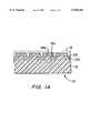
- FIGS. 1-4show a disc-like device 10 for use in an EAS detection system in accordance with the principles of present invention.
- the disc-like device 10is a compact disc or "CD", which is a laser-read or optically read data storing device on which coded information, audio, video or textual information in digital form can be stored.
- the disc-like device 10comprises a disc-like substrate 12 of a light-transmissive material or light transmissive synthetic resin such as polycarbonate (PC), polymethyl methacrylate resin (PMMA), etc.
- the substrate 12is injection molded and has an information signal pattern which has been formed as a pattern of pits 18a and lands 18b on a surface thereof.
- a magnetic material layer 20is deposited on the information signal pattern of the substrate 12, by way of evaporation, sputtering, etc.
- the layer 20is formed over the surface of the pits 18a and lands 18b so as to cover the signal pattern on the substrate 12 and has reflective properties.
- the thickness of the layer 20is dependent upon having enough volume of magnetic material so that a signal therefrom can be provided and detected by an EAS detection system.
- a protective layer 16may be formed over the magnetic material layer 20 by a spin coating process to protect the surface of the disc-like device 10.
- the protective layer 16has a thickness of several microns and is formed of transparent resin such as ultraviolet ray curing resin or lacquer.
- the magnetic material layer 20 of the disc-like device 10 of FIG. 1permits detection of the device 10 in an EAS detection system in the following manner:
- the EAS detection systemcan detect the unique harmonic signal of the layer 20 and can then generate an alarm.
- the magnetic material layer 20 incorporated in the device 10helps to decrease the number of steps required to provide EAS protection for the device.
- the device 10can then be immediately displayed in a retail establishment. Further, with the layer 20 formed on the surface of the device 10, as illustrated in FIG. 1, EAS surveillance of the device 10 is now possible without detection of EAS means by a customer, employee, etc. This prevents both customers and employees from knowing how the device 10 is protected and further hinders theft.
- a reflective layer 14is deposited on the information signal pattern of the substrate 12, by way of evaporation, sputtering, etc., and is formed over the surface of the pits 18a and lands 18b so as to cover the signal pattern on the disc-like substrate 12.
- the reflective layer 14, for example,can be made of a metallic material, such as an alloy of aluminum or silver and can have a thickness in the range of 600 ⁇ to 1500 ⁇ .
- a magnetic material layer 22is then deposited on the reflective layer 14 on the substrate 12.
- a protective layer 16is then formed over the magnetic material layer 22.
- FIG. 3illustrates a further modification of the device 10 of the invention.
- the device 10comprises a disc-like substrate 12, a reflective layer 14, a magnetic material layer 24, a semi-hard material layer 26 and a protective layer 16.
- the magnetic material layer 24 with the semi-hard material layer 26 deposited thereonallows for the device 10 to be detectable and non-detectable by an EAS detection system.
- the magnetic material layer 24In order for the device 10 as shown in FIG. 3 to be either detectable or non-detectable by an EAS detection system, the magnetic material layer 24 must be in either an activated or deactivated state.
- an AC degaussing fieldis applied to demagnetize the semi-hard material layer 26. Such demagnetization enables the magnetic layer 24 to generate a unique harmonic signal. Thus when the layer 24 is subjected to an alternating magnetic field in the EAS detection area, the EAS detection system will then detect the presence of the device 10.
- the magnetic material layer 24must be deactivated.
- the semi-hard material layer 26is subjected to a pulsed or DC magnetizing field. Accordingly, if a pulsed or DC field of an initial level of about 200 Oe or above is applied to the device 10, the layer 26 is sufficiently magnetized so that significantly reduced or no harmonic signals from the layer 24 are detectable. Upon removing the DC field, the layer 26 remains magnetized thereby rendering the device 10 nondetectable.
- the semi-hard material layer 26is again demagnetized. This is accomplished by applying an AC degaussing field to the layer 26.
- an AC degaussing fieldabove about 200 Oe is applied, the layer 26 becomes sufficiently demagnetized to allow the magnetic material layer 24 to generate a harmonic signal thereby once again rendering the device 10 detectable.
- the deactivatable layer 26could also be applied to the structure of FIG. 1 where the magnetic layer 20 serves as both the reflective layer as well as the EAS magnetic active component. This is shown in FIG. 1A.
- FIGS. 1 to 3may be constructed or laminated back to back to provide the ability to read both sides of the CD and provide EAS protection as well as deactivation and reactivation capability.
- FIG. 4Another modified embodiment of the double sided CD device 10 is illustrated in FIG. 4, with a first dis-like substrate 50 and a second disc-like substrate 70 having a magnetic layer 54 sandwiched between protective layers 60 and 76, respectively, of the two substrates. More particularly, the protective layer 60, with first top and bottom surfaces 64 and 66, and the protective layer 76 with second top and bottom surfaces 80 and 82 enclose the magnetic layer 54 between the first top surface 64 of the layer 60 and the second top surface 80 of the layer 76.
- the device 10has its first substrate 50 with a first signal pattern of pits 62a and lands 62b and a reflective layer 58 and its second substrate 70 with a second signal pattern of pits 78a and lands 78b and a reflective layer 74.
- the device 10 of FIG. 4permits information to be stored and read from two combined substrates while also providing detection of the device by an EAS detection system. Deactivation and reactivation of the FIG. 4 device may also be provided by including a semi-hard layer of magnetic material adjacent the soft magnetic layer 54.
- the magnetic layers 20, 22, 24 and 54 of the device 10 as illustrated in FIGS. 1-4can comprise an EAS material which can either be a non-magnetostrictive or magnetostrictive material.
- non-magnetostrictive materialswhich can be used for the magnetic material layer are any number of soft amorphous magnetic materials.
- amorphous transition metal-metalloid compositions containing Co, Fe, Si and B with an atomic ratio of Co to Fe of 94:6can be used.
- Such compositionsinclude Co 74 .26 Fe 4 .74 Si 2 .1 B 18 .9 and Co 70 .5 Fe 4 .5 Si 15 B 10 .
- Other materials which may be usedinclude a low magnetostrictive CoNiFeB based amorphous material composition such as Co 56 Ni 16 Fe 8 B 20 and Co 44 Ni 24 Fe 12 B 20 .
- amorphous transition metal-metal compositionsselected from the group comprising Co, Zr and Nb such as Co 90 Zr 5 Nb 5 .
- Crystalline material having a NiFe composition such as Ni 81 Fe 19may also be used for the magnetic layer.
- Magnetostrictive materials which can be used as the magnetic material layerinclude amorphous materials comprising compositions containing Co, Fe, Si and B with examples including Co 39 .5 Fe 39 .5 Si 2 .1 B 18 .9 and Co 47 .4 Fe 31 .6 Si 2 .1 B 18 .9.
- compositions containing Co, Fe, Ni and Bsuch as Co 20 Fe 40 Ni 20 B 20 and Co 10 Fe 60 Ni 10 B 20 .
- Magnetic materialscan be selected from compositions including Co, Zr and Nb with an example being Co 90 Zr 10 .
- Magnetostrictive material of a crystalline materialmay also be used with compositions selected from the group comprising Ni and Fe.
- An exampleincludes Ni 45 Fe 55 .
- stress relief annealingmay be required to enable the material to respond to a field.
- the temperature range and time for annealingis dependent upon the type of magnetostrictive material being used, its desired thickness and the temperature range of the other materials comprising the disc-like device (e.g., the type of plastic substrate, the type of material in the reflective material layer, etc.).
- semi-hard material layer 26semi-hard material compositions similar to those sold under the trademarks "Vicalloy” or “Crovac” and available commercially from Vacuumschmelze GmbH of Hanau, Germany, may be used. Examples of such compositions include Co 80 Ni 20 and Co 48 Fe 41 V 11 .
- the layer 26can have a thickness in the range of about 0.5 microns to 25 microns and a coercivity above about 20 Oe and below about 500 Oe.
- the device 10 as illustrated in FIGS. 1-4can be used in an EAS detection system 100, as illustrated in FIG. 5A, which detects the presence of the device 10 in a particular surveillance area 118, e.g., an exit area of a retail establishment, as indicated by broken lines.
- a particular surveillance area 118e.g., an exit area of a retail establishment, as indicated by broken lines.
- the transmitter portion of the system 100comprises a frequency generator 102 with an output being fed to a power amplifier 104 which in turn feeds a field generating coil 106.
- the coil 106establishes an alternating magnetic field of a desired frequency in the surveillance area 118.
- the amplitude of the fieldvaries depending upon the system parameters, such as the type of coil, the size of the surveillance area 118, etc. The amplitude, however, must exceed a minimum field so that the device 10 in the surveillance area 118 will detect a field above the device threshold.
- the receiving portion of the system 100includes a field receiving coil 112, the output of which is applied to a receiver 110.
- the receiver 110detects a particular harmonic content in signals received from the coil 112 in a prescribed range and resulting from the device 10, the receiver 110 furnishes a triggering alarm to an alarm unit 108.
- the unit 108activates an alarm to indicate that unauthorized removal of the device 10 is being attempted through the surveillance area 118.
- the device 10 as illustrated in FIG. 3also has the ability to be detectable and non-detectable by the EAS detection system 100 by means of an activating/deactivating system 200.
- an activating and/or deactivating area 210is established by an activating/deactivating unit 208.
- the deactivation field generator 202drives a generating coil 206 which establishes a pulsed or DC magnetizing field through the area 210.
- the initial amplitude of the pulsed or DC magnetizing fieldmust exceed a minimum level so that the device 10 in the area will be exposed to a magnetizing field of a sufficient level to magnetize the semi-hard material layer 26 of the device 10 to render the device 10 non-detectable.
- the activation field generator 204is inactive.
- the device 10 as illustrated in FIG. 3can then also be rendered detectable by the EAS detection system 100.
- An activation field generator 204drives the generating coil 206 to establish an AC degaussing field through the area 210.
- the initial amplitude of the activation fieldmust exceed a minimum level so that the device 10 in the area will be exposed to a decaying AC field of a sufficient level to demagnetize the semi-hard material layer 26 to render the device 10 detectable.
- the deactivation field generator 202is inactive.
- the device 10 as illustrated in FIG. 3, however,is not limited to the above deactivation and reactivation processes but can be activated, deactivated and reactivated in a variety of ways.
- a multi-pole magnetcan be used to alter the magnetic state of the semi-hard material layer 26.
- the magnetic material layer as well as the semi-hard material layerextend over the surface of the disc-like device 10.
- these layerscan extend over only selected areas of the disc-like substrate and can be formed in a variety of patterns or designs, such as strips, circles, etc.
- the device 10 and application of the layers thereofcan also be made by any number of manufacturing processes.
- a variety of different types of evaporation and sputtering methodscan be used for applying a magnetic material layer to the disc-like device 10.
- a planar type sputtering apparatuscan be used.
- the sputtering methodcan also include a facing target cathode type, an ion-beam sputtering type, a laser-beam sputtering type or a magnetron sputtering apparatus.
- the device 10 of the present inventioncan be any type and/or size CD, such as CD-ROM, audio CD, mini-CDs, CD-R, DVD, DVD-ROM, CD-I, etc.
- the disc-like device 10 of the present inventionis also not limited to the present illustrative case, but can also include a phonograph record or any type of disc-shaped information medium.
Landscapes
- Physics & Mathematics (AREA)
- Engineering & Computer Science (AREA)
- Automation & Control Theory (AREA)
- Computer Security & Cryptography (AREA)
- Electromagnetism (AREA)
- General Physics & Mathematics (AREA)
- Burglar Alarm Systems (AREA)
- Optical Record Carriers And Manufacture Thereof (AREA)
- Magnetic Record Carriers (AREA)
Abstract
Description
Claims (5)
Priority Applications (8)
| Application Number | Priority Date | Filing Date | Title |
|---|---|---|---|
| US08/699,494US5940362A (en) | 1996-08-19 | 1996-08-19 | Disc device having a magnetic layer overweighing the information signal pattern for electronic article surveillance |
| BR9711823-0ABR9711823A (en) | 1996-08-19 | 1997-08-08 | Disc type device with areas material. |
| JP51265498AJP2002524022A (en) | 1996-08-19 | 1997-08-08 | Disc-shaped device with EAS material |
| EP97938133AEP0917712A4 (en) | 1996-08-19 | 1997-08-08 | Disc-like device with eas material |
| PCT/US1997/013785WO1998010386A2 (en) | 1996-08-19 | 1997-08-08 | Disc-like device with eas material |
| AU40530/97AAU729410B2 (en) | 1996-08-19 | 1997-08-08 | Disc-like device with EAS material |
| CA002263483ACA2263483C (en) | 1996-08-19 | 1997-08-08 | Disc-like device with eas material |
| ARP970103744AAR009264A1 (en) | 1996-08-19 | 1997-08-19 | DISCOIDAL DEVICE WITH MATERIAL FOR ELECTRONIC ARTICLE SURVEILLANCE |
Applications Claiming Priority (1)
| Application Number | Priority Date | Filing Date | Title |
|---|---|---|---|
| US08/699,494US5940362A (en) | 1996-08-19 | 1996-08-19 | Disc device having a magnetic layer overweighing the information signal pattern for electronic article surveillance |
Publications (1)
| Publication Number | Publication Date |
|---|---|
| US5940362Atrue US5940362A (en) | 1999-08-17 |
Family
ID=24809575
Family Applications (1)
| Application Number | Title | Priority Date | Filing Date |
|---|---|---|---|
| US08/699,494Expired - LifetimeUS5940362A (en) | 1996-08-19 | 1996-08-19 | Disc device having a magnetic layer overweighing the information signal pattern for electronic article surveillance |
Country Status (7)
| Country | Link |
|---|---|
| US (1) | US5940362A (en) |
| EP (1) | EP0917712A4 (en) |
| JP (1) | JP2002524022A (en) |
| AR (1) | AR009264A1 (en) |
| AU (1) | AU729410B2 (en) |
| BR (1) | BR9711823A (en) |
| CA (1) | CA2263483C (en) |
Cited By (12)
| Publication number | Priority date | Publication date | Assignee | Title |
|---|---|---|---|---|
| WO2003091754A1 (en)* | 2002-04-26 | 2003-11-06 | Bibliotheca Rfid Library Systems Ag | Securing and identifying label and the production and use thereof |
| US6775839B1 (en) | 2002-03-15 | 2004-08-10 | O'brien Patrick J. | Optical storage device with print layer surface feature |
| US20050200485A1 (en)* | 2004-02-09 | 2005-09-15 | One World Technologies Limited | Article containing anti-theft device |
| US20070214507A1 (en)* | 2005-11-23 | 2007-09-13 | Selinfreund Richard H | Anti-theft system for optical products |
| US20070282378A1 (en)* | 2002-12-09 | 2007-12-06 | Ferro Solutions, Inc. | Apparatus and method utilizing magnetic field |
| US20090062886A1 (en)* | 2002-12-09 | 2009-03-05 | Ferro Solutions, Inc. | Systems and methods for delivering electrical energy in the body |
| US7569952B1 (en) | 2003-04-18 | 2009-08-04 | Ferro Solutions, Inc. | High efficiency, inductive vibration energy harvester |
| US20100163433A1 (en)* | 2005-04-05 | 2010-07-01 | Harald Horn | Method and device for measuring the condition of steel structures |
| US7808236B1 (en) | 2002-12-09 | 2010-10-05 | Ferro Solutions, Inc. | Energy harvester utilizing external magnetic field |
| CN105448021A (en)* | 2015-10-08 | 2016-03-30 | 宁波讯强电子科技有限公司 | Acousto-magnetic anti-theft soft tag having upper surface with concave-convex graph or character and manufacturing method thereof |
| US20160156103A1 (en)* | 2013-06-27 | 2016-06-02 | Lg Innotek Co., Ltd. | Receiving antenna and wireless power receiving device including the same |
| US11784502B2 (en) | 2014-03-04 | 2023-10-10 | Scramoge Technology Limited | Wireless charging and communication board and wireless charging and communication device |
Citations (15)
| Publication number | Priority date | Publication date | Assignee | Title |
|---|---|---|---|---|
| US3905040A (en)* | 1973-02-12 | 1975-09-09 | Philips Corp | Magnetic domain storage disk |
| US4729940A (en)* | 1986-05-16 | 1988-03-08 | Cbs Inc. | Method of manufacturing master for optical information carrier |
| US4808291A (en)* | 1987-09-09 | 1989-02-28 | Denton Vacuum Inc. | Apparatus for coating compact disks |
| US4870524A (en)* | 1984-07-06 | 1989-09-26 | Furukawa Aluminum Co., Ltd. | Substrate for rigid disk storage media |
| US4929928A (en)* | 1987-02-20 | 1990-05-29 | Ab Aros Avancerad Butikskontroll | Magnetized ink, paint or dye used on merchandise to prevent theft |
| US4931313A (en)* | 1987-09-03 | 1990-06-05 | Sony Corporation | Method of forming a protective film for an optical recording medium |
| US4967184A (en)* | 1989-09-19 | 1990-10-30 | Eastman Kodak Company | Computer disk with security protection |
| US5012380A (en)* | 1989-08-24 | 1991-04-30 | Eastman Kodak Company | Article surveillance protection of flexible magnetic computer data storage disks |
| US5031162A (en)* | 1987-09-30 | 1991-07-09 | Deutsche Thomson-Brandt Gmbh | Magneto-optical recorded medium with a transparent substrate layer |
| US5083112A (en)* | 1990-06-01 | 1992-01-21 | Minnesota Mining And Manufacturing Company | Multi-layer thin-film eas marker |
| US5135376A (en)* | 1989-05-15 | 1992-08-04 | Sony Corporation | Optical-disk manufacturing device |
| US5181020A (en)* | 1990-03-23 | 1993-01-19 | Unitika, Ltd. | Thin-film magnetic material and process of production thereof |
| US5347508A (en)* | 1992-04-22 | 1994-09-13 | Minnesota Mining And Manufacturing Company | Optical information storage disk for use with electronic article surveillance systems |
| US5409756A (en)* | 1991-09-25 | 1995-04-25 | Sony Corporation | Optical disc with corrosion-resistant metallic reflective layer |
| US5499015A (en)* | 1994-09-28 | 1996-03-12 | Sensormatic Electronics Corp. | Magnetomechanical EAS components integrated with a retail product or product packaging |
Family Cites Families (3)
| Publication number | Priority date | Publication date | Assignee | Title |
|---|---|---|---|---|
| JPS586536A (en)* | 1981-07-01 | 1983-01-14 | Pioneer Electronic Corp | Optical disc |
| DE4242992B4 (en)* | 1992-12-18 | 2004-01-29 | Meto International Gmbh | Arrangement for securing an article, in particular a recording disk such as a CD disk |
| DE4440314A1 (en)* | 1994-11-11 | 1996-05-15 | Esselte Meto Int Gmbh | Marking element for protecting articles against theft |
- 1996
- 1996-08-19USUS08/699,494patent/US5940362A/ennot_activeExpired - Lifetime
- 1997
- 1997-08-08CACA002263483Apatent/CA2263483C/ennot_activeExpired - Fee Related
- 1997-08-08AUAU40530/97Apatent/AU729410B2/ennot_activeCeased
- 1997-08-08EPEP97938133Apatent/EP0917712A4/ennot_activeWithdrawn
- 1997-08-08JPJP51265498Apatent/JP2002524022A/enactivePending
- 1997-08-08BRBR9711823-0Apatent/BR9711823A/enunknown
- 1997-08-19ARARP970103744Apatent/AR009264A1/enunknown
Patent Citations (15)
| Publication number | Priority date | Publication date | Assignee | Title |
|---|---|---|---|---|
| US3905040A (en)* | 1973-02-12 | 1975-09-09 | Philips Corp | Magnetic domain storage disk |
| US4870524A (en)* | 1984-07-06 | 1989-09-26 | Furukawa Aluminum Co., Ltd. | Substrate for rigid disk storage media |
| US4729940A (en)* | 1986-05-16 | 1988-03-08 | Cbs Inc. | Method of manufacturing master for optical information carrier |
| US4929928A (en)* | 1987-02-20 | 1990-05-29 | Ab Aros Avancerad Butikskontroll | Magnetized ink, paint or dye used on merchandise to prevent theft |
| US4931313A (en)* | 1987-09-03 | 1990-06-05 | Sony Corporation | Method of forming a protective film for an optical recording medium |
| US4808291A (en)* | 1987-09-09 | 1989-02-28 | Denton Vacuum Inc. | Apparatus for coating compact disks |
| US5031162A (en)* | 1987-09-30 | 1991-07-09 | Deutsche Thomson-Brandt Gmbh | Magneto-optical recorded medium with a transparent substrate layer |
| US5135376A (en)* | 1989-05-15 | 1992-08-04 | Sony Corporation | Optical-disk manufacturing device |
| US5012380A (en)* | 1989-08-24 | 1991-04-30 | Eastman Kodak Company | Article surveillance protection of flexible magnetic computer data storage disks |
| US4967184A (en)* | 1989-09-19 | 1990-10-30 | Eastman Kodak Company | Computer disk with security protection |
| US5181020A (en)* | 1990-03-23 | 1993-01-19 | Unitika, Ltd. | Thin-film magnetic material and process of production thereof |
| US5083112A (en)* | 1990-06-01 | 1992-01-21 | Minnesota Mining And Manufacturing Company | Multi-layer thin-film eas marker |
| US5409756A (en)* | 1991-09-25 | 1995-04-25 | Sony Corporation | Optical disc with corrosion-resistant metallic reflective layer |
| US5347508A (en)* | 1992-04-22 | 1994-09-13 | Minnesota Mining And Manufacturing Company | Optical information storage disk for use with electronic article surveillance systems |
| US5499015A (en)* | 1994-09-28 | 1996-03-12 | Sensormatic Electronics Corp. | Magnetomechanical EAS components integrated with a retail product or product packaging |
Cited By (20)
| Publication number | Priority date | Publication date | Assignee | Title |
|---|---|---|---|---|
| US6775839B1 (en) | 2002-03-15 | 2004-08-10 | O'brien Patrick J. | Optical storage device with print layer surface feature |
| US7317398B2 (en) | 2002-04-26 | 2008-01-08 | Bibliotheca Rfid Library Systems Ag | Security and identification label and the production and use thereof |
| WO2003091754A1 (en)* | 2002-04-26 | 2003-11-06 | Bibliotheca Rfid Library Systems Ag | Securing and identifying label and the production and use thereof |
| US20060101272A1 (en)* | 2002-04-26 | 2006-05-11 | Phillip Muller | Securing and identifying label and the production and use thereof |
| US7808236B1 (en) | 2002-12-09 | 2010-10-05 | Ferro Solutions, Inc. | Energy harvester utilizing external magnetic field |
| US7952349B2 (en) | 2002-12-09 | 2011-05-31 | Ferro Solutions, Inc. | Apparatus and method utilizing magnetic field |
| US20070282378A1 (en)* | 2002-12-09 | 2007-12-06 | Ferro Solutions, Inc. | Apparatus and method utilizing magnetic field |
| US20090062886A1 (en)* | 2002-12-09 | 2009-03-05 | Ferro Solutions, Inc. | Systems and methods for delivering electrical energy in the body |
| US20100253089A1 (en)* | 2002-12-09 | 2010-10-07 | Ferro Solutions, Inc. | Energy harvester utilizing external magnetic field |
| US7569952B1 (en) | 2003-04-18 | 2009-08-04 | Ferro Solutions, Inc. | High efficiency, inductive vibration energy harvester |
| US20050200485A1 (en)* | 2004-02-09 | 2005-09-15 | One World Technologies Limited | Article containing anti-theft device |
| US20100163433A1 (en)* | 2005-04-05 | 2010-07-01 | Harald Horn | Method and device for measuring the condition of steel structures |
| US7919971B2 (en)* | 2005-04-05 | 2011-04-05 | Harald Horn | Method and device for measuring the condition of steel structures |
| AU2006231357B2 (en)* | 2005-04-05 | 2011-04-14 | Harald Horn | Method and device for measuring the condition of steel structures |
| US20070214507A1 (en)* | 2005-11-23 | 2007-09-13 | Selinfreund Richard H | Anti-theft system for optical products |
| US20160156103A1 (en)* | 2013-06-27 | 2016-06-02 | Lg Innotek Co., Ltd. | Receiving antenna and wireless power receiving device including the same |
| US9997962B2 (en)* | 2013-06-27 | 2018-06-12 | Lg Innotek Co., Ltd. | Receiving antenna and wireless power receiving device including the same |
| US10468918B2 (en)* | 2013-06-27 | 2019-11-05 | Lg Innotek Co., Ltd. | Receiving antenna and wireless power receiving device including the same |
| US11784502B2 (en) | 2014-03-04 | 2023-10-10 | Scramoge Technology Limited | Wireless charging and communication board and wireless charging and communication device |
| CN105448021A (en)* | 2015-10-08 | 2016-03-30 | 宁波讯强电子科技有限公司 | Acousto-magnetic anti-theft soft tag having upper surface with concave-convex graph or character and manufacturing method thereof |
Also Published As
| Publication number | Publication date |
|---|---|
| EP0917712A2 (en) | 1999-05-26 |
| BR9711823A (en) | 1999-10-13 |
| AR009264A1 (en) | 2000-04-12 |
| AU4053097A (en) | 1998-03-26 |
| AU729410B2 (en) | 2001-02-01 |
| CA2263483A1 (en) | 1998-03-12 |
| JP2002524022A (en) | 2002-07-30 |
| EP0917712A4 (en) | 2001-02-07 |
| CA2263483C (en) | 2005-10-18 |
Similar Documents
| Publication | Publication Date | Title |
|---|---|---|
| WO1998010386A2 (en) | Disc-like device with eas material | |
| JP3332461B2 (en) | Optical information storage disk for use in electronic article surveillance system and magnetic marker used for such disk | |
| AU696579B2 (en) | Magnetomechanical eas components integrated with a retail product or product packaging | |
| US5762377A (en) | Method of authenticating an item and an apparatus for authenticating an item | |
| US5940362A (en) | Disc device having a magnetic layer overweighing the information signal pattern for electronic article surveillance | |
| US4967184A (en) | Computer disk with security protection | |
| US4910625A (en) | Article surveillance apparatus and systems for computer data disks | |
| US6614750B2 (en) | Optical recordable disk security system | |
| US6822569B1 (en) | Insertable electronic article surveillance label | |
| US20050242956A1 (en) | Magnetic marker for use in product authentication, and detector for reading the marker | |
| US6693542B2 (en) | Electronic article surveillance markers for recorded media | |
| US7823781B2 (en) | Method and system for source tagging an optical storage device | |
| US6525661B2 (en) | Electronic article surveillance markers for optically recorded media | |
| CA2414367A1 (en) | Device for changing the status of dual status magnetic electronic article surveillance markers | |
| AU718179B2 (en) | Magnetomechanical EAS components integrated with a retail product or product packaging | |
| RU2332713C1 (en) | Electromagnetic label deactivator | |
| HK1014292A (en) | Optical information storage disk for use with electronic article surveillance systems | |
| JP2002362669A (en) | Disk storage unit with tag |
Legal Events
| Date | Code | Title | Description |
|---|---|---|---|
| AS | Assignment | Owner name:SENSORMATIC ELECTRONICS CORPORATION, FLORIDA Free format text:ASSIGNMENT OF ASSIGNORS INTEREST;ASSIGNORS:PLONSKY, CHRISTOPHER B.;HO, WING;REEL/FRAME:008173/0407 Effective date:19960816 | |
| STCF | Information on status: patent grant | Free format text:PATENTED CASE | |
| AS | Assignment | Owner name:SENSORMATIC ELECTRONICS CORPORATION, FLORIDA Free format text:MERGER/CHANGE OF NAME;ASSIGNOR:SENSORMATIC ELECTRONICS CORPORATION;REEL/FRAME:012991/0641 Effective date:20011113 | |
| FPAY | Fee payment | Year of fee payment:4 | |
| FPAY | Fee payment | Year of fee payment:8 | |
| AS | Assignment | Owner name:SENSORMATIC ELECTRONICS, LLC,FLORIDA Free format text:MERGER;ASSIGNOR:SENSORMATIC ELECTRONICS CORPORATION;REEL/FRAME:024213/0049 Effective date:20090922 Owner name:SENSORMATIC ELECTRONICS, LLC, FLORIDA Free format text:MERGER;ASSIGNOR:SENSORMATIC ELECTRONICS CORPORATION;REEL/FRAME:024213/0049 Effective date:20090922 | |
| FPAY | Fee payment | Year of fee payment:12 | |
| AS | Assignment | Owner name:ADT SERVICES GMBH, SWITZERLAND Free format text:ASSIGNMENT OF ASSIGNORS INTEREST;ASSIGNOR:SENSORMATIC ELECTRONICS, LLC;REEL/FRAME:029894/0856 Effective date:20130214 | |
| AS | Assignment | Owner name:TYCO FIRE & SECURITY GMBH, SWITZERLAND Free format text:MERGER;ASSIGNOR:ADT SERVICES GMBH;REEL/FRAME:030290/0731 Effective date:20130326 |