US5940345A - Combinational logic feedback circuit to ensure correct power-on-reset of a four-bit synchronous shift register - Google Patents
Combinational logic feedback circuit to ensure correct power-on-reset of a four-bit synchronous shift registerDownload PDFInfo
- Publication number
- US5940345A US5940345AUS08/990,126US99012697AUS5940345AUS 5940345 AUS5940345 AUS 5940345AUS 99012697 AUS99012697 AUS 99012697AUS 5940345 AUS5940345 AUS 5940345A
- Authority
- US
- United States
- Prior art keywords
- signal
- circuit
- select signals
- page
- invalidity
- Prior art date
- Legal status (The legal status is an assumption and is not a legal conclusion. Google has not performed a legal analysis and makes no representation as to the accuracy of the status listed.)
- Expired - Lifetime
Links
Images


Classifications
- G—PHYSICS
- G11—INFORMATION STORAGE
- G11C—STATIC STORES
- G11C8/00—Arrangements for selecting an address in a digital store
- G11C8/12—Group selection circuits, e.g. for memory block selection, chip selection, array selection
- G—PHYSICS
- G11—INFORMATION STORAGE
- G11C—STATIC STORES
- G11C8/00—Arrangements for selecting an address in a digital store
- G11C8/04—Arrangements for selecting an address in a digital store using a sequential addressing device, e.g. shift register, counter
Definitions
- This inventionrelates generally to integrated circuits, and, more particularly, to a circuit for an integrated circuit memory to provide a power-on-reset function, as well as to provide the function of determining whether a plurality of page select signals for selecting a page of memory define a valid state.
- One approach for memory page access to implement the burst modeis to use a burst counter in combination with a postdecoder circuit to generate the above-mentioned page select signals. The generated page select signals are then applied to the memory array to access the selected page.
- Another approach taken in the arthas been to use a combination of a decoder circuit, and a synchronous shift register. However, such a configuration may generate an invalid output under certain circumstances, for example during power-up.
- an integrated circuit having a memoryincludes a page enable circuit, and a reset signal generating means.
- the page enable circuitis configured to generate a plurality of page select signals to enable a selected one of a plurality of pages of the memory.
- the reset signal generating meansis configured to generate a reset signal when the page select signals (preferably, collectively) define an invalid state. The reset signal is then fed back to the page enable circuit, which is further configured to "reset" in response to the reset signal. When "reset", the page select signals are generated in a valid state.
- the inventionemploys feedback based on the page select signals to ensure that the page enable circuit outputs a valid state (i.e., in a preferred embodiment, a state which enables only a selected one of the memory pages at a time).
- a valid statei.e., in a preferred embodiment, a state which enables only a selected one of the memory pages at a time.
- the inventionis effective both during power-up of the integrated circuit, as well as during normal operation thereafter.
- the page enable circuitincludes a synchronous shift register which generates the page select signals in accordance with a clock signal (i.e., synchronously).
- a clock signali.e., synchronously
- FIG. 1is a simplified block diagram view of an integrated circuit in accordance with the present invention.
- FIG. 2is a simplified schematic diagram view, showing in greater detail, one embodiment of a combinational circuit shown in FIG. 1 in block diagram form.
- FIG. 3is a simplified schematic and block diagram view showing, in greater detail, a deglitch circuit shown in FIG. 1 in block diagram form.
- FIG. 4is a simplified schematic diagram view illustrating, in greater detail, the deglitch circuit shown in FIG. 3.
- FIG. 5is a simplified schematic diagram view showing one embodiment of the delay block shown in FIG. 4.
- FIGS. 6A-6Eare timing diagrams showing waveforms in accordance with the operation of the present invention.
- FIG. 1shows an integrated circuit, such as a static random access memory (SRAM) 10, in accordance with the present invention.
- integrated circuit 10may be a 2 Megabit (64k ⁇ 32-bit) synchronous pipelined cache SRAM device of the type in which the memory is segregated into four pages of 16k ⁇ 32-bit capacity each.
- Integrated circuit 10may include a memory array and access logic block 12, a decoder 14, a page select circuit 16, and means or circuit 18 for generating a reset signal, designated RESETB in the figures.
- Memory array and access logic 12includes (i) a memory array, which may be arranged in 32-bit words in multiple pages, and (ii) an access logic block.
- the memory arrayis provided for storage and retrieval of data, as is well-known.
- the access logic blockmay be responsive to a plurality of page select signals PAGE0, PAGE1, PAGE2, and PAGE3 for enabling a selected one of the memory pages of the memory array for such data storage and retrieval operations thereto.
- memory array and access logic block 12may comprise conventional and well-known structures, and will therefore not be described in further detail.
- Decoder 14provides a conventional decoding function. That is, in the illustrated embodiment, decoder 14 receives two (2) digital input signals, namely Z0 and Z1, and asserts, in response thereto, one of four output lines. The signal on each output line is associated, with a respective page of memory. Decoder 14 may comprise conventional decoding structures well-known to those of ordinary skill in the art.
- Page select circuit 16is configured to generate a plurality of page select signals, designated PAGE0, PAGE1, PAGE2, and PAGE3, to enable a selected one of the plurality of pages of memory 12. Circuit 16 also generates the complement of the page select signals, namely, PAGE0, PAGE1, PAGE2, and PAGE3.
- page select circuit 16comprises a synchronous shift register 20 that includes individual registers 20 0 , 20 1 , 20 2 , and 20 3 .
- the synchronous shift registeris configured to receive a clock signal in accordance with which respective input signals (from decoder 14) are transferred to respective output signals on output lines thereof. These output signals define the page select signals (PAGE0, PAGE1, PAGE2, and PAGE3).
- synchronous shift register 20is further configured to receive a reset signal, designated RESETB, from reset signal generating means 18 and, in response thereto, generate the page select signals in a valid state.
- a valid statemay be a state in which only one of the pages of memory are enabled at a time.
- decoder 14may be provided with signals Z0, Z1 in advance of the ti me that the clock signal causes shift register 20 to capture the data on its respective input lines. That is, the decoding function, in the preferred embodiment can be done before the decoded output is needed, so that when the clock signal comes, the page select signals are already decoded and available. This aspect permits a faster clock-to-select time.
- the decoding functionoccurs with every clock signal (i.e., the counter must be incremented using the clock signal delay1!, and then the counter output is decoded using the decoder delay2!). This counter/post decoder configuration may be slower than the configuration (decoder/shift register) employed in the preferred embodiment.
- the approach according to the inventioni.e., a combination decoder/burst shift register
- a preferred embodiment according to the inventionmay implemented using 20% less semiconductor die area than an embodiment employing a counter/decoder combination.
- Means or circuit 18is configured to generate a reset signal, designated RESETB, when the page select signals, namely PAGE0, PAGE1, PAGE2 and PAGE3, define an invalid state.
- the invalid stateis one of the plurality of states other than the valid states set forth above.
- the complement of the page select signalsare processed.
- reset signal generating means 18may include a combinational circuit 22, and a deglitch circuit 24.
- Combinational circuit 22may be configured to assert an invalidity signal when the page select signals define an invalid state.
- Deglitch circuit 24may be configured to inhibit or suppress asserted conditions of the invalidity signal that are not indicative of an invalid state (i.e., "false reset signals") to generate the reset signal RESETB. For example, due to the state transitions of the page select signals, momentary "glitches” or “false reset signals” may be output from combinational circuit 22. Deglitch circuit 24 inhibits or suppresses such false reset signals, particularly those of a type that have a pulsewidth up to and including a predetermined pulsewidth.
- deglitch circuit 24inhibits "false reset signals,” it outputs a true reset signal indicative of an invalid state, as defined by the page select signals output from synchronous shift register 20.
- deglitch circuit 24 in circuit 18removes the requirement that the propagation delay of every path through combinational circuit 22 be equalized. This results in a simpler and smaller design for circuit 22.
- FIG. 2shows one embodiment of combinational circuit 22.
- Circuit 22may include a first exclusive OR gate 26, a second exclusive OR gate 28, a first NAND gate 30, a second NAND gate 32, and a third NAND gate 34.
- the complement of page select signals PAGE0, PAGE1, PAGE2, and PAGE3, in a constructed embodiment,are applied to gates 26, 28, 30, and 32 to generate an invalidity signal 36.
- the invalidity signal 36is, in one embodiment, a logic high when the page select signals define a valid state. When the plurality of page select signals assume an invalid state, even momentarily, then the invalidity signal will, in the illustrated embodiment, transition to a logic low state. It should be appreciated that the circuit illustrated in FIG. 2 is but one realization operative to generate an invalidity signal 36 when the page select signals collectively define an invalid state.
- combinational circuit 22may be any logic circuit which performs the function defined as follows:
- the number of possible output statesequals 2 N .
- the number of valid states, Kshould be less than the total number of possible output states, namely, K ⁇ 2 N .
- FIG. 3shows a simplified schematic and block diagram view of deglitch circuit 24, may which include a delay circuit 38, a NOR gate 40, and an inverter 42.
- the delay circuit 38is configured to receive the invalidity signal 36, and generate (in response thereto) a delayed version of the invalidity signal, designated 36 delayed .
- NOR gate 40is configured to receive the invalidity signal 36, and the delayed version of the invalidity signal 36 delayed , and generate an output, which is provided to inverter gate 42.
- Inverter gate 42then inverts its input to generate the reset signal, designated RESETB, on an output terminal thereof.
- Delay circuit 38is specifically configured to delay invalidity signal 36 by an amount equal to T ⁇ . This action results in a situation where the delayed version of invalidity signal 36 delayed is offset relative to the invalidity signal 36 by a predetermined time interval, namely T ⁇ .
- the predetermined time interval T ⁇is substantially equal to the longest pulsewidth "glitch” that can be inhibited or suppressed by the deglitch circuit 24. Selection of the predetermined time interval T ⁇ depends on several factors including (i) the time interval that it takes for any one of the page select signals to transition from a first state to a second state or vice-versa (i.e., the "edge rate" of any one of the page select signals), and (ii) the respective propagation delays of the various paths through combinational circuit 22 (as well as the respective differences in propagation delay between any two paths in circuit 22).
- FIG. 4shows a simplified schematic diagram of deglitch circuit 24, showing delay circuit 38 in greater detail.
- Delay circuit 38may include an even number of inverting buffers 44 0 , 44 1 , . . . , 44 5 , as well as a plurality of capacitors, designated C.
- An even number of inverting buffers 44maintains the logical sense of the invalidity signal 36 (i.e., a logic high invalidity signal 36 will be maintained as a logic high 36 delayed , and a logic low invalidity signal 36 will be maintained as a logic low 36 delayed ).
- each inverting bufferhas, on its output, one capacitor coupled to ground, and another capacitor coupled to the positive power supply.
- FIG. 5shows delay circuit 38, shown in FIG. 3 in block diagram form, in even greater detail.
- the capacitors C coupled to each inverting buffer outputmay be formed using PMOS transistors P 1 -P 12 , and NMOS transistors N 1 -N 12 , respectively configured as capacitors (e.g., the gate terminal configured as a first capacitor terminal, the drain and source terminals being connected together to define a second capacitor terminal wherein the gate oxide forms the capacitor dielectric).
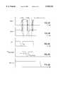
- FIGS. 6A-6Eare timing diagrams showing the operation of the present invention.
- FIGS. 6A, and 6Bshow exemplary waveforms for the page select signals designated PAGE1, and PAGE2 (see FIG. 1).
- page select signals PAGE0, and PAGE3are defined as LOW (logic 0) in the timing diagram.
- a "glitch”i.e., an asserted condition of invalidity signal 36 that is NOT indicative of an invalid state
- FIG. 6Dshows glitch 50 illustrated in FIG. 6C, delayed by a predetermined amount T ⁇ .
- FIG. 6Eshows the output of inverter 42.
- both inputs to NOR gate 40must be low. This condition will not be satisfied for glitches having a pulsewidth less than T ⁇ . Therefore, as shown in FIG. 6E, glitch 50 is effectively filtered out (suppressed or inhibited).
- both page select signals PAGE1, and PAGE2assume active high states (i.e., collectively defining an invalid state in a constructed embodiment). This condition persists for greater than a T ⁇ time interval--thus it will not be suppressed or inhibited by deglitch circuit 24. Therefore, as shown in FIG. 6E, the reset signal RESETB will be taken low, which is an active state in the illustrative embodiment.
- An integrated circuit in accordance with the present inventionprovides state-of-the-art performance levels in generating needed page select signals.
- the inventionalso performs a power-on-reset function in the preferred embodiment, and provides the function of monitoring for invalid states during normal operation. In either case, the invention is operative to "reset" the page enable circuit (e.g., the synchronous shift register in the preferred embodiment) should an invalid state be detected. Once "reset,” the page enable circuit outputs a valid state.
- combinational circuit 22, and deglitch circuit 24may be replaced by synchronous logic or an alternative type of logic to fully complementary CMOS.
- the method and apparatus of performing the power-on-reset functioncan be applied to any synchronous circuit and/or circuit designed using output latches which have a number of predefined valid output states which are less than the total number of possible output states.
Landscapes
- Engineering & Computer Science (AREA)
- Microelectronics & Electronic Packaging (AREA)
- Electronic Switches (AREA)
Abstract
Description
Claims (13)
Priority Applications (1)
| Application Number | Priority Date | Filing Date | Title |
|---|---|---|---|
| US08/990,126US5940345A (en) | 1997-12-12 | 1997-12-12 | Combinational logic feedback circuit to ensure correct power-on-reset of a four-bit synchronous shift register |
Applications Claiming Priority (1)
| Application Number | Priority Date | Filing Date | Title |
|---|---|---|---|
| US08/990,126US5940345A (en) | 1997-12-12 | 1997-12-12 | Combinational logic feedback circuit to ensure correct power-on-reset of a four-bit synchronous shift register |
Publications (1)
| Publication Number | Publication Date |
|---|---|
| US5940345Atrue US5940345A (en) | 1999-08-17 |
Family
ID=25535793
Family Applications (1)
| Application Number | Title | Priority Date | Filing Date |
|---|---|---|---|
| US08/990,126Expired - LifetimeUS5940345A (en) | 1997-12-12 | 1997-12-12 | Combinational logic feedback circuit to ensure correct power-on-reset of a four-bit synchronous shift register |
Country Status (1)
| Country | Link |
|---|---|
| US (1) | US5940345A (en) |
Cited By (3)
| Publication number | Priority date | Publication date | Assignee | Title |
|---|---|---|---|---|
| US20070024332A1 (en)* | 2005-07-28 | 2007-02-01 | Standard Microsystems Corporation | All MOS power-on-reset circuit |
| US20070126479A1 (en)* | 2005-09-28 | 2007-06-07 | Hynix Semiconductor Inc. | Semiconductor memory device with signal aligning circuit |
| US20080164909A1 (en)* | 2007-01-08 | 2008-07-10 | Darmin Jin | De-Glitch Circuit |
Citations (34)
| Publication number | Priority date | Publication date | Assignee | Title |
|---|---|---|---|---|
| US4044339A (en)* | 1975-12-15 | 1977-08-23 | Honeywell Inc. | Block oriented random access memory |
| US4443847A (en)* | 1981-02-05 | 1984-04-17 | International Business Machines Corporation | Page addressing mechanism |
| US4446381A (en)* | 1982-04-22 | 1984-05-01 | Zilog, Inc. | Circuit and technique for initializing the state of bistable elements in an integrated electronic circuit |
| US4453212A (en)* | 1981-07-13 | 1984-06-05 | Burroughs Corporation | Extended address generating apparatus and method |
| US4590551A (en)* | 1981-08-24 | 1986-05-20 | Burroughs Corporation | Memory control circuit for subsystem controller |
| US4631707A (en)* | 1982-08-31 | 1986-12-23 | Nec Corporation | Memory circuit with power supply voltage detection means |
| US4788454A (en)* | 1986-07-21 | 1988-11-29 | Oki Electric Industry Co., Ltd. | Power-on reset circuit |
| US4789967A (en)* | 1986-09-16 | 1988-12-06 | Advanced Micro Devices, Inc. | Random access memory device with block reset |
| US4797584A (en)* | 1986-02-18 | 1989-01-10 | Sgs Microelettronica S.P.A. | Power-on reset circuit for MOS logic devices |
| EP0320142A2 (en)* | 1987-11-27 | 1989-06-14 | Tosoh Corporation | Preparation of poly (arylene sulfide) |
| US4873671A (en)* | 1988-01-28 | 1989-10-10 | National Semiconductor Corporation | Sequential read access of serial memories with a user defined starting address |
| US4874965A (en)* | 1987-11-30 | 1989-10-17 | Sgs Microelettronica S.P.A. | Circuital device for the power-on reset of digital integrated circuits in MOS technology |
| US4886984A (en)* | 1987-03-27 | 1989-12-12 | Nec Corporation | Prohibition circuit upon power-on event |
| US4888498A (en)* | 1988-03-24 | 1989-12-19 | Texas Instruments Incorporated | Integrated-circuit power-up pulse generator circuit |
| US4924375A (en)* | 1987-10-23 | 1990-05-08 | Chips And Technologies, Inc. | Page interleaved memory access |
| US4969126A (en)* | 1988-01-14 | 1990-11-06 | Mitsubishi Denki Kabushiki Kaisha | Semiconductor memory device having serial addressing and operating method thereof |
| US4970408A (en)* | 1989-10-30 | 1990-11-13 | Motorola, Inc. | CMOS power-on reset circuit |
| US4983857A (en)* | 1989-07-31 | 1991-01-08 | Sgs-Thomson Microelectronics, Inc. | Power-up reset circuit |
| US5047989A (en)* | 1989-03-10 | 1991-09-10 | Intel Corporation | Chapter mode selection apparatus for MOS memory |
| US5115146A (en)* | 1990-08-17 | 1992-05-19 | Sgs-Thomson Microelectronics, Inc. | Power-on reset circuit for controlling test mode entry |
| US5121358A (en)* | 1990-09-26 | 1992-06-09 | Sgs-Thomson Microelectronics, Inc. | Semiconductor memory with power-on reset controlled latched row line repeaters |
| US5231603A (en)* | 1985-07-22 | 1993-07-27 | Microchip Technology Incorporated | Variable page ROM |
| US5237219A (en)* | 1992-05-08 | 1993-08-17 | Altera Corporation | Methods and apparatus for programming cellular programmable logic integrated circuits |
| US5243233A (en)* | 1992-09-24 | 1993-09-07 | Altera Corporation | Power on reset circuit having operational voltage trip point |
| US5343085A (en)* | 1992-04-09 | 1994-08-30 | Kabushiki Kaisha Toshiba | Power-on reset system and a semiconductor memory device incorporating same |
| US5359233A (en)* | 1990-09-28 | 1994-10-25 | Dallas Semiconductor Corporation | Reset monitor for detection of power failure and external reset |
| US5361371A (en)* | 1988-12-21 | 1994-11-01 | Mitsubishi Denki Kabushiki Kaisha | Microprocessor with reset execution from an arbitrary address |
| US5404543A (en)* | 1992-05-29 | 1995-04-04 | International Business Machines Corporation | Method and system for reducing an amount of power utilized by selecting a lowest power mode from a plurality of power modes |
| US5410514A (en)* | 1993-03-23 | 1995-04-25 | International Business Machines Corporation | Single clock memory having a page mode |
| US5477176A (en)* | 1994-06-02 | 1995-12-19 | Motorola Inc. | Power-on reset circuit for preventing multiple word line selections during power-up of an integrated circuit memory |
| US5485428A (en)* | 1994-05-17 | 1996-01-16 | Winbond Electronics Corp. | Memory device with page select capability |
| US5621692A (en)* | 1994-05-24 | 1997-04-15 | Winbond Electronics Corporation | Memory device with page select capability |
| EP1026182A1 (en)* | 1997-10-07 | 2000-08-09 | Santen Pharmaceutical Co., Ltd | Four component copolymer and the ocular lens made thereof |
| EP1796512A2 (en)* | 2004-08-23 | 2007-06-20 | David Preston | Outdoor chair |
- 1997
- 1997-12-12USUS08/990,126patent/US5940345A/ennot_activeExpired - Lifetime
Patent Citations (35)
| Publication number | Priority date | Publication date | Assignee | Title |
|---|---|---|---|---|
| US4044339A (en)* | 1975-12-15 | 1977-08-23 | Honeywell Inc. | Block oriented random access memory |
| US4443847A (en)* | 1981-02-05 | 1984-04-17 | International Business Machines Corporation | Page addressing mechanism |
| US4453212A (en)* | 1981-07-13 | 1984-06-05 | Burroughs Corporation | Extended address generating apparatus and method |
| US4590551A (en)* | 1981-08-24 | 1986-05-20 | Burroughs Corporation | Memory control circuit for subsystem controller |
| US4446381A (en)* | 1982-04-22 | 1984-05-01 | Zilog, Inc. | Circuit and technique for initializing the state of bistable elements in an integrated electronic circuit |
| US4631707A (en)* | 1982-08-31 | 1986-12-23 | Nec Corporation | Memory circuit with power supply voltage detection means |
| US5231603A (en)* | 1985-07-22 | 1993-07-27 | Microchip Technology Incorporated | Variable page ROM |
| US4797584A (en)* | 1986-02-18 | 1989-01-10 | Sgs Microelettronica S.P.A. | Power-on reset circuit for MOS logic devices |
| US4788454A (en)* | 1986-07-21 | 1988-11-29 | Oki Electric Industry Co., Ltd. | Power-on reset circuit |
| US4789967A (en)* | 1986-09-16 | 1988-12-06 | Advanced Micro Devices, Inc. | Random access memory device with block reset |
| US4886984A (en)* | 1987-03-27 | 1989-12-12 | Nec Corporation | Prohibition circuit upon power-on event |
| US4924375A (en)* | 1987-10-23 | 1990-05-08 | Chips And Technologies, Inc. | Page interleaved memory access |
| EP0320142A2 (en)* | 1987-11-27 | 1989-06-14 | Tosoh Corporation | Preparation of poly (arylene sulfide) |
| US4874965A (en)* | 1987-11-30 | 1989-10-17 | Sgs Microelettronica S.P.A. | Circuital device for the power-on reset of digital integrated circuits in MOS technology |
| US4969126A (en)* | 1988-01-14 | 1990-11-06 | Mitsubishi Denki Kabushiki Kaisha | Semiconductor memory device having serial addressing and operating method thereof |
| US4873671A (en)* | 1988-01-28 | 1989-10-10 | National Semiconductor Corporation | Sequential read access of serial memories with a user defined starting address |
| US4888498A (en)* | 1988-03-24 | 1989-12-19 | Texas Instruments Incorporated | Integrated-circuit power-up pulse generator circuit |
| US5361371A (en)* | 1988-12-21 | 1994-11-01 | Mitsubishi Denki Kabushiki Kaisha | Microprocessor with reset execution from an arbitrary address |
| US5047989A (en)* | 1989-03-10 | 1991-09-10 | Intel Corporation | Chapter mode selection apparatus for MOS memory |
| US4983857A (en)* | 1989-07-31 | 1991-01-08 | Sgs-Thomson Microelectronics, Inc. | Power-up reset circuit |
| US4970408A (en)* | 1989-10-30 | 1990-11-13 | Motorola, Inc. | CMOS power-on reset circuit |
| US5115146A (en)* | 1990-08-17 | 1992-05-19 | Sgs-Thomson Microelectronics, Inc. | Power-on reset circuit for controlling test mode entry |
| US5121358A (en)* | 1990-09-26 | 1992-06-09 | Sgs-Thomson Microelectronics, Inc. | Semiconductor memory with power-on reset controlled latched row line repeaters |
| US5526318A (en)* | 1990-09-26 | 1996-06-11 | Sgs-Thompson Microelectronics, Inc. | Semiconductor memory with power-on reset controlled latched row line repeaters |
| US5359233A (en)* | 1990-09-28 | 1994-10-25 | Dallas Semiconductor Corporation | Reset monitor for detection of power failure and external reset |
| US5343085A (en)* | 1992-04-09 | 1994-08-30 | Kabushiki Kaisha Toshiba | Power-on reset system and a semiconductor memory device incorporating same |
| US5237219A (en)* | 1992-05-08 | 1993-08-17 | Altera Corporation | Methods and apparatus for programming cellular programmable logic integrated circuits |
| US5404543A (en)* | 1992-05-29 | 1995-04-04 | International Business Machines Corporation | Method and system for reducing an amount of power utilized by selecting a lowest power mode from a plurality of power modes |
| US5243233A (en)* | 1992-09-24 | 1993-09-07 | Altera Corporation | Power on reset circuit having operational voltage trip point |
| US5410514A (en)* | 1993-03-23 | 1995-04-25 | International Business Machines Corporation | Single clock memory having a page mode |
| US5485428A (en)* | 1994-05-17 | 1996-01-16 | Winbond Electronics Corp. | Memory device with page select capability |
| US5621692A (en)* | 1994-05-24 | 1997-04-15 | Winbond Electronics Corporation | Memory device with page select capability |
| US5477176A (en)* | 1994-06-02 | 1995-12-19 | Motorola Inc. | Power-on reset circuit for preventing multiple word line selections during power-up of an integrated circuit memory |
| EP1026182A1 (en)* | 1997-10-07 | 2000-08-09 | Santen Pharmaceutical Co., Ltd | Four component copolymer and the ocular lens made thereof |
| EP1796512A2 (en)* | 2004-08-23 | 2007-06-20 | David Preston | Outdoor chair |
Cited By (7)
| Publication number | Priority date | Publication date | Assignee | Title |
|---|---|---|---|---|
| US20070024332A1 (en)* | 2005-07-28 | 2007-02-01 | Standard Microsystems Corporation | All MOS power-on-reset circuit |
| US20070126479A1 (en)* | 2005-09-28 | 2007-06-07 | Hynix Semiconductor Inc. | Semiconductor memory device with signal aligning circuit |
| US20090231933A1 (en)* | 2005-09-28 | 2009-09-17 | Hwang Hur | Semiconductor memory device with signal aligning circuit |
| US7804723B2 (en)* | 2005-09-28 | 2010-09-28 | Hynix Semiconductor Inc. | Semiconductor memory device with signal aligning circuit |
| US8054702B2 (en) | 2005-09-28 | 2011-11-08 | Hynix Semiconductor Inc. | Semiconductor memory device with signal aligning circuit |
| US20080164909A1 (en)* | 2007-01-08 | 2008-07-10 | Darmin Jin | De-Glitch Circuit |
| US7557643B2 (en) | 2007-01-08 | 2009-07-07 | Sandisk Corporation | De-glitch circuit |
Similar Documents
| Publication | Publication Date | Title |
|---|---|---|
| US7279935B2 (en) | Method and apparatus for reducing clock enable setup time in a multi-enabled clock gating circuit | |
| US8344780B2 (en) | Flip-flop circuits and system including the same | |
| US7015600B2 (en) | Pulse generator circuit and semiconductor device including same | |
| US5264737A (en) | One-shot signal generation circuitry for use in semiconductor memory integrated circuit | |
| EP0401521A2 (en) | Semiconductor memory device | |
| US5493530A (en) | Ram with pre-input register logic | |
| US5977809A (en) | Programmable non-overlap clock generator | |
| US5765194A (en) | Timing consistent dynamic compare with force miss circuit | |
| US5198709A (en) | Address transition detector circuit | |
| US6215722B1 (en) | Command latency circuit for programmable SLDRAM and latency control method therefor | |
| US5146111A (en) | Glitch-proof powered-down on chip receiver with non-overlapping outputs | |
| KR20030014358A (en) | Techniques to synchronously operate a synchronous memory | |
| US5940345A (en) | Combinational logic feedback circuit to ensure correct power-on-reset of a four-bit synchronous shift register | |
| US6392474B1 (en) | Circuit for filtering single event effect (see) induced glitches | |
| US6373290B1 (en) | Clock-delayed pseudo-NMOS domino logic | |
| US7961009B2 (en) | Domino logic block having data holding function and domino logic including the domino logic block | |
| US6294939B1 (en) | Device and method for data input buffering | |
| KR100486261B1 (en) | Skew Free Dual Rail Bus Driver | |
| Franch et al. | A 640-ps, 0.25-/spl mu/m CMOS, 16/spl times/64-b three-port register file | |
| JP3270411B2 (en) | Address decoding device | |
| JP3842571B2 (en) | Flip-flop circuit | |
| US6819134B2 (en) | Decoding circuit for wafer burn-in test | |
| US6603338B1 (en) | Device and method for address input buffering | |
| US6667637B1 (en) | Dynamic logic circuit with beta controllable noise margin | |
| US6232798B1 (en) | Self-resetting circuit timing correction |
Legal Events
| Date | Code | Title | Description |
|---|---|---|---|
| AS | Assignment | Owner name:CYPRESS SEMICONDUCTOR CORPORATION, CALIFORNIA Free format text:ASSIGNMENT OF ASSIGNORS INTEREST;ASSIGNOR:DAVIDSON, COLIN A.;REEL/FRAME:008930/0254 Effective date:19971211 | |
| STCF | Information on status: patent grant | Free format text:PATENTED CASE | |
| FPAY | Fee payment | Year of fee payment:4 | |
| FPAY | Fee payment | Year of fee payment:8 | |
| FPAY | Fee payment | Year of fee payment:12 | |
| AS | Assignment | Owner name:MORGAN STANLEY SENIOR FUNDING, INC., NEW YORK Free format text:SECURITY INTEREST;ASSIGNORS:CYPRESS SEMICONDUCTOR CORPORATION;SPANSION LLC;REEL/FRAME:035240/0429 Effective date:20150312 | |
| AS | Assignment | Owner name:SPANSION LLC, CALIFORNIA Free format text:PARTIAL RELEASE OF SECURITY INTEREST IN PATENTS;ASSIGNOR:MORGAN STANLEY SENIOR FUNDING, INC., AS COLLATERAL AGENT;REEL/FRAME:039708/0001 Effective date:20160811 Owner name:CYPRESS SEMICONDUCTOR CORPORATION, CALIFORNIA Free format text:PARTIAL RELEASE OF SECURITY INTEREST IN PATENTS;ASSIGNOR:MORGAN STANLEY SENIOR FUNDING, INC., AS COLLATERAL AGENT;REEL/FRAME:039708/0001 Effective date:20160811 | |
| AS | Assignment | Owner name:MONTEREY RESEARCH, LLC, CALIFORNIA Free format text:ASSIGNMENT OF ASSIGNORS INTEREST;ASSIGNOR:CYPRESS SEMICONDUCTOR CORPORATION;REEL/FRAME:040911/0238 Effective date:20160811 | |
| AS | Assignment | Owner name:MORGAN STANLEY SENIOR FUNDING, INC., NEW YORK Free format text:CORRECTIVE ASSIGNMENT TO CORRECT THE 8647899 PREVIOUSLY RECORDED ON REEL 035240 FRAME 0429. ASSIGNOR(S) HEREBY CONFIRMS THE SECURITY INTERST;ASSIGNORS:CYPRESS SEMICONDUCTOR CORPORATION;SPANSION LLC;REEL/FRAME:058002/0470 Effective date:20150312 |