US5940151A - Liquid crystal display and method for fabricating the same - Google Patents
Liquid crystal display and method for fabricating the sameDownload PDFInfo
- Publication number
- US5940151A US5940151AUS08/843,470US84347097AUS5940151AUS 5940151 AUS5940151 AUS 5940151AUS 84347097 AUS84347097 AUS 84347097AUS 5940151 AUS5940151 AUS 5940151A
- Authority
- US
- United States
- Prior art keywords
- pixel
- tft
- conductivity type
- tfts
- layer
- Prior art date
- Legal status (The legal status is an assumption and is not a legal conclusion. Google has not performed a legal analysis and makes no representation as to the accuracy of the status listed.)
- Expired - Lifetime
Links
Images


Classifications
- G—PHYSICS
- G02—OPTICS
- G02F—OPTICAL DEVICES OR ARRANGEMENTS FOR THE CONTROL OF LIGHT BY MODIFICATION OF THE OPTICAL PROPERTIES OF THE MEDIA OF THE ELEMENTS INVOLVED THEREIN; NON-LINEAR OPTICS; FREQUENCY-CHANGING OF LIGHT; OPTICAL LOGIC ELEMENTS; OPTICAL ANALOGUE/DIGITAL CONVERTERS
- G02F1/00—Devices or arrangements for the control of the intensity, colour, phase, polarisation or direction of light arriving from an independent light source, e.g. switching, gating or modulating; Non-linear optics
- G02F1/01—Devices or arrangements for the control of the intensity, colour, phase, polarisation or direction of light arriving from an independent light source, e.g. switching, gating or modulating; Non-linear optics for the control of the intensity, phase, polarisation or colour
- G02F1/13—Devices or arrangements for the control of the intensity, colour, phase, polarisation or direction of light arriving from an independent light source, e.g. switching, gating or modulating; Non-linear optics for the control of the intensity, phase, polarisation or colour based on liquid crystals, e.g. single liquid crystal display cells
- G02F1/133—Constructional arrangements; Operation of liquid crystal cells; Circuit arrangements
- G02F1/1333—Constructional arrangements; Manufacturing methods
- G02F1/1345—Conductors connecting electrodes to cell terminals
- G02F1/13454—Drivers integrated on the active matrix substrate
- G—PHYSICS
- G09—EDUCATION; CRYPTOGRAPHY; DISPLAY; ADVERTISING; SEALS
- G09G—ARRANGEMENTS OR CIRCUITS FOR CONTROL OF INDICATING DEVICES USING STATIC MEANS TO PRESENT VARIABLE INFORMATION
- G09G3/00—Control arrangements or circuits, of interest only in connection with visual indicators other than cathode-ray tubes
- G09G3/20—Control arrangements or circuits, of interest only in connection with visual indicators other than cathode-ray tubes for presentation of an assembly of a number of characters, e.g. a page, by composing the assembly by combination of individual elements arranged in a matrix no fixed position being assigned to or needed to be assigned to the individual characters or partial characters
- G09G3/34—Control arrangements or circuits, of interest only in connection with visual indicators other than cathode-ray tubes for presentation of an assembly of a number of characters, e.g. a page, by composing the assembly by combination of individual elements arranged in a matrix no fixed position being assigned to or needed to be assigned to the individual characters or partial characters by control of light from an independent source
- G09G3/36—Control arrangements or circuits, of interest only in connection with visual indicators other than cathode-ray tubes for presentation of an assembly of a number of characters, e.g. a page, by composing the assembly by combination of individual elements arranged in a matrix no fixed position being assigned to or needed to be assigned to the individual characters or partial characters by control of light from an independent source using liquid crystals
- G09G3/3611—Control of matrices with row and column drivers
- G09G3/3685—Details of drivers for data electrodes
- G09G3/3688—Details of drivers for data electrodes suitable for active matrices only
Definitions
- the present inventionrelates to a semiconductor device, and more particularly, to a liquid crystal display (LCD) and a method for fabricating the same.
- LCDliquid crystal display
- an amorphous silicon(a--Si) has been a choice of material for a thin film transistor (TFT) to fabricate an LCD.
- a polysiliconbecomes a substitute for the amorphous silicon for the TFT because the polysilicon has a carrier (electron or hole) mobility that is higher than that of the amorphous silicon.
- the polysilicon TFThas an advantage of forming the driving circuit on the LCD panel during the fabrication of pixels.
- CMOScomplimentary metal-oxide-semiconductor
- the polysilicon TFT-LCDsince most of the drive circuit is formed with the polysilicon TFT, driver ICs(Intergrated Circuits) do not need to be bonded to the LCD panel. Thus, fabricating the drive circuit and the pixel on the LCD panel simultaneously becomes a feasible process. Furthermore, the polysilicon TFT can be fabricated on a larger glass substrate at low temperature below 500° C. due to a recently developed crystallization technique using a eximer laser. As a result, the polysilicon TFT can be formed at similar fabrication temperature with the amorphous silicon TFT.
- the polysilicon TFT-LCDemploys a structure where the drive circuit portion and pixel portion are formed on the same glass substrate.
- the TFT at the drive circuitcan be switched at high speed due to the high carrier mobility of the polysilicon TFT.
- a TFT having a lightly doped drain (LDD), offset or dual gate structurehas been suggested in order to reduce the off-current to a desirable level at the pixel portion.
- LDDlightly doped drain
- FIG. 1is an equivalent circuit diagram of a conventional LCD in which a drive circuit is formed on an insulating substrate.
- a plurality of signal lines 5 and scanning lines 4intersect with each other and are arranged in a matrix form at the pixel portion on a transparent substrate.
- a pixel electrode 6 and a TFT 9 for driving the pixel portionare formed at the intersection.
- a common electrode 8 for displaying picturesis formed on the other transparent substrate.
- a storage capacitor 7is formed to be electrically parallel with the pixel electrode 6 and the common electrode 8.
- a gate drive circuit 1 and a data drive circuit 2are formed at the periphery of the pixel portion. These circuits apply a desirable signal to the pixel portion.
- the gate drive circuit 1 and the data drive circuit 2are simultaneously formed on the same insulating substrate.
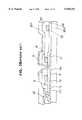
- FIG. 2Ais a plan view of the pixel portion of a conventional LCD
- FIG. 2Bis a cross-sectional view taken along line I--I' of FIG. 2A.
- a signal line 40 and a scanning line 50intersect or cross each other on an insulating substrate 1000, and a source region 11S at the TFT is connected to the signal line 40.
- a drain region 11Dis connected to a pixel electrode 15.
- the drain region 11D and a first storage capacitor electrode 17are formed as one layer.
- a gate electrode 14 connected to the scanning line 50is formed on a gate insulating layer 100.
- a second storage capacitor electrode 18forms a storage capacitor together with the first storage capacitor electrode 17.
- a gate insulating layer 100is formed between the first and second capacitor electrodes.
- the second storage capacitor electrode 18 and the gate electrode 14are formed of a same material and the same layer.
- Source and drain regions 11S and 11D of the TFTare heavily doped regions with N-type or P-type ions.
- An LDD region 12is formed adjacent to the heavily doped region so as to reduce the leakage current when the TFT is at the off-state.
- Reference numeral 200designates an interlevel insulating layer, and reference numeral 300 designates a passivation layer.
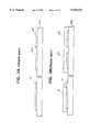
- FIGS. 3A to 3Hare cross-sectional views showing process steps of fabricating the conventional LCD.
- the left portionshows the TFT for the pixel and the right portion shows the CMOS-TFT for the drive circuit portion.
- a polysiliconis formed on a substrate 1000 and patterned to form semiconductor layers 10', 20n' and 20p' on the pixel and drive circuit portions, respectively.
- the semiconductor layer 10'corresponds to the pixel portion, and the semiconductor layers 20n' and 20p' are for the drive circuit portion.
- the semiconductor layers 20n' and 20p'are used to form an N-type TFT and P-type TFT, respectively.
- a predetermined type of impurityis selectively implanted into the semiconductor layer 10' (which will be an active layer 10 at the pixel portion) to form a first storage capacitor electrode 17.
- the type of impurity to be dopedis the same as that of the source and drain regions which are formed as follows. For example, for a pixel TFT of an N-type, N-type impurity ions are selectively implanted only into the first storage capacitor electrode region using a photoresist 61 as a mask. Thereafter, the photoresist 61 is removed, and the first storage capacitor electrode region is irradiated by a laser or heated by a conventional method in order to activate the impurity ions implanted in the previous step.
- an insulating material including silicon oxide or silicon nitrideis deposited on the substrate 1000 including the first storage capacitor electrode 17 to form a gate insulating layer 100.
- a metalsuch as Al, Al alloy, Mo, or Cr is deposited on the gate insulating layer 100 and patterned through photolithography to form a gate electrode 14 for the pixel TFT and gate electrodes 24n and 24p for the drive circuit TFT on the gate insulating layer 100.
- a second storage capacitor electrode 18is also formed at the pixel portion. That is, the gate electrode 14 and the second storage capacitor electrode 18 are formed using the same material.
- N-type impuritiesare doped lightly into the exposed surface over the substrate to form the LDD TFT.
- the gate electrodes 14, 24n, and 24pact as masks to block the ions.
- an n - layer 12', 21' and 22' and channel layers 10, 20n, and 20pare formed in semiconductor layers 10', 20n', and 20p' (shown in FIG. 3A), respectively.
- n - impuritiesare doped with a low ion implantation energy
- an insulating layer including a silicon oxide layer or a silicon nitride layer and a metal layer such as Al, Al alloy, Mo, or Crare sequentially formed on the substrate.
- the insulating layer and the metal layerare patterned simultaneously.
- the gate insulating layer 100 and the gate electrodes 14, 24n, and 24pare formed in the same patterning process, and a portion of the semiconductor layers 10', 20n', and 20p' are exposed as shown in FIG. 3X.
- N-type impuritiesare doped with a low ion implantation energy into the exposed surface over the substrate.
- the exposed portions of the semiconductor layers 12', 21', and 22'which are not blocked by the gate electrodes, is lightly doped with impurities and becomes the n - layer. Furthermore, the channel layers 10, 20n, and 20p are formed at portions of the semiconductor layer below the gate electrodes 14, 24n, and 24p. Thus, in the alternative embodiment, the impurities are directly implanted into the semiconductor layer unlike the process shown in FIG. 3D.
- a photoresistis coated on the exposed surface over the substrate and patterned to form a photoresist pattern 62 to cover a P-type TFT region at the drive circuit and the gate electrode 14 and a portion of the semiconductor layer at the pixel TFT.
- N-type impuritiesare heavily doped using the photoresist pattern as a mask.
- the photoresist pattern 62is formed on the pixel portion to cover the gate electrode 14 and a portion of the semiconductor layer, the impurities are selectively doped into a portion of the n - layer. Accordingly, source 11S and drain 11D are formed to have a heavily doped n + layer and a lightly doped n - layer 12 in the semiconductor layer at the pixel portion to complete an LDD structure.
- the P-type TFT regionis covered with photoresist pattern 62 and the n + doping is carried out on a portion of the semiconductor layer at the N-type TFT region to form source and drain regions 21S and 21D and an N-type channel 20n. Accordingly, the TFT having an LDD structure with the n + and n - layers is formed at the pixel portion, while the N-type TFT having the n + layer and the P-type TFT having the p + layer are formed at the drive circuit portion.
- photoresist pattern 62As shown in FIG. 3F, after the photoresist pattern 62 is removed, another photoresist is coated on the substrate and patterned to form a photoresist pattern 63.
- the photoresist pattern 63covers a large portion and exposes the P-type TFT region at the drive circuit portion. Then, P-type impurities are heavily doped into the substrate using photoresist pattern 63 as a mask.
- source and drain regions 23S and 23Dare formed having a p + layer, and a P-type channel region 20p is formed in a portion of the semiconductor layer at the P-type TFT region in the drive circuit portion.
- the above-mentioned impurity doping methodis called a counter doping.
- the concentration of the ion doped into the semiconductoris approximately 10 16 ⁇ 10 18 /cm 3 for n 31 doping and about 10 10 ⁇ 10 21 /cm 3 for p - doping. Accordingly, the n - layer is converted to p + layer by the p + doping.
- an insulating layerfor example, a silicon nitride layer, is formed on the exposed surface over the substrate 1000 to form an inter-layer insulating layer 200. Then, the inter-layer insulating layer 200 is patterned to form contact holes over a source region 11S at the pixel portion and source regions 21S and 23S and drain regions 21D and 23D at the drive circuit portion. A metal such as Al is deposited on the substrate and patterned to form a signal line 40 connected to the source region 11S at the pixel portion.
- a metal line 25 for connecting the source and drain regions at the drive circuitis formed in order to form a CMOS-TFT with the N-type and P-type TFTs at the drive circuit portion. Accordingly, the LDD structured TFT and the CMOS-TFT are formed at the pixel portion and the drive circuit portion, respectively.
- an insulating layeris formed on the exposed surface over the substrate to form a passivation layer 300.
- a portion of the gate insulating layer 100, the inter-layer insulating layer 200, and the passivation layer 300 on a drain region 11Dare selectively etched through photolithography to form a contact hole over the drain region 11D.
- an Indium Tin Oxide (ITO)is deposited on the exposed surface over the substrate and patterned to form a pixel electrode 15.
- a top plate including a color filteris fabricated through a separate process. Then, after the two plates are bonded to each other, liquid crystal is injected between the two plates to complete the TFT-LCD.
- the above-described conventional TFT-LCDemploys a CMOS-TFT as a drive circuit TFT for a better circuit performance. Also, the storage capacitor is formed on the pixel portion using the gate insulating layer formed between the active region and the gate electrode to improve the picture quality. Thus, the conventional method for fabricating the TFT-LCD requires at least nine steps of the photoresist and mask alignment to fabricate the TFT substrate.
- the present inventionis directed to an LCD and a method for fabricating the same that substantially obviates one or more of the problems due to limitations and disadvantages of the related art.
- An object of the present inventionis to provide an LCD having a reduced number of fabrication steps, thereby improving productivity.
- a liquid crystal displayincludes a plurality of pixel TFTs in a matrix form on an insulating substrate, a plurality of drive circuit TFTs having a CMOS structure on the peripheral portion of the pixel TFTs, the drive circuit TFTs including a first conductivity type TFT having the structure the same as the pixel TFT and a second conductivity type TFT has a structure different from the pixel TFT, a plurality of signal lines being connected to the pixel TFTs, and a plurality of scanning lines being intersected to the signal lines.
- a liquid crystal displayin another aspect of the present invention, includes a plurality of pixel TFTs in a matrix form on an insulating substrate, the pixel TFTs having an LDD region or offset region, source and drain electrode, and a first and second storage capacitor electrode, a plurality of drive circuit TFTs having a CMOS structure, the peripheral portion of the pixel TFTs a first conductivity type TFT having source and drain electrode below an active layer, a second-type TFT having source and drain electrode on the active layer, a plurality of signal lines being connected to the pixel TFTs, and a plurality of scanning lines being intersected to the signal lines.
- a method for fabricating a liquid crystal displayincludes the steps of forming a pixel TFT and a first conductivity type TFT at a drive circuit portion having the same conductivity as a channel at the pixel TFT over a substrate, forming active layers at the pixel TFT and the first conductivity type TFT and for a second conductivity type TFT at the drive circuit portion, forming gate electrodes over the substrate and a storage capacitor electrode at the pixel TFT, doping the first impurity to the active layers at the pixel TFT and the first conductivity type TFT and the second conductivity type TFT at the drive circuit portion, injecting a second impurity to the active layer at the second conductivity type TFT at the drive circuit portion, forming an insulating layer over the substrate, the insulating layer having contact holes over a drain electrode at the pixel TFT and source and drain regions at the drive circuit portion, and forming an ITO connecting the drain electrode at the pixel TFT and connecting the first and second conductivity type
- the methodforming a first semiconductor layer and a first metal layer over an insulating substrate, patterning the first semiconductor layer and the first metal layer to form source and drain electrodes at a pixel TFT portion and a first conductivity type TFT at the drive circuit portion, the first conductivity type TFT having the same conductivity as a channel at pixel TFTS, forming an active layer on an exposed surface over the substrate, patterning the active layer at the pixel TFT and the first and second conductivity type TFTs at the drive circuit portion, forming a first insulating layer and a second metal layer on an exposed surface over the substrate, patterning the first insulating layer and the second metal layer to form gate electrodes on the active layer, injecting a first impurity into the active layer using the gate electrodes as masks, injecting a second impurity into the active layer of the second conductivity type TFT at the drive circuit to form source and drain regions of the second conductivity type TFT at the drive circuit portion, the second impurity being do
- FIG. 1is an equivalent circuit diagram of an LCD including drive circuits
- FIGS. 2A and 2Bare a plan view and a cross-sectional view, respectively, illustrating a pixel portion of a conventional LCD
- FIGS. 3A to 3H and FIG. 3Xare cross-sectional views illustrating the process steps of fabricating a conventional LCD
- FIGS. 4A and 4Bare a plan view and a cross-sectional view, respectively, illustrating a pixel portion of an LCD according to the present invention
- FIGS. 5A and 5Bare a plan view and a cross-sectional view, respectively, illustrating a CMOS-TFT structure forming a drive circuit portion of an LCD according to the present invention.
- FIGS. 6A to 6Eare cross-sectional views illustrating the process steps of fabricating an LCD according to the present invention.
- an N-type TFTis formed at a pixel portion, and a CMOS-TFT is formed at a drive circuit portion.
- channel regions of TFTs at the drive circuit and the pixel portionhave the same conductivity for a stagger type, and channel regions of TFTs at the drive circuit and the pixel portion have the opposite conductivity to each other for a coplanar type.
- the TFT-LCD having the aforementioned structures according to the present inventionwill be explained below.
- the pixel TFTis an N-type.
- FIG. 4Ais a plan view illustrating the pixel portion at the LCD according to the present invention
- FIG. 4Bis a cross-sectional view along the line II--II' in FIG. 4A.
- a scanning line 50 and a signal line 40intersect or cross each other on an insulating layer 1000, and a stagger type TFT is formed at the intersection.
- Source and drain electrodes 11S and 11D at the TFTare formed as a dual-level or double-level layer using an N-doped silicon (n + --Si) layer and a metal layer.
- a first storage capacitor electrode 17 and drain electrode 11Dare formed as the same layer.
- a storage capacitorincludes a second storage capacitor electrode 18 over the first storage capacitor electrode 17.
- a gate insulating layer 100is formed between the first and second capacitor electrodes.
- a contact holeis formed at a predetermined portion of a passivation layer 300, and a transparent pixel electrode 15 is connected to the drain electrode 11D through the contact hole.
- a lightly doped LDD region or undoped offset region 12is formed between a channel region 10 and source/drain electrodes 11S and 11D at the TFT in order to reduce the leakage current when the TFT is at an off state. If the length of the offset region is longer than about 1 ⁇ m, the on-current of the offset TFT decrease. On the other hand, the doping is not needed if the length of the offset region is less than about 1 ⁇ m.
- FIG. 5Ais a plan view of the drive circuit portion at the TFT-LCD according to the present invention
- FIG. 5Bis a cross-sectional view taken along the line III--III' in FIG. 5A.
- the TFT-LCDincludes two CMOS-TFT having a gate electrode and source/drain electrodes on insulating substrate 1000.
- the N-type TFT at the drive circuitis formed as the stagger type.
- the P-type TFT at the drive circuitis formed as the coplanar type different from the pixel TFT.
- the N-type TFT at the drive circuithas source and drain electrodes 21S and 21D forming a dual-level layer with a doped silicon (n + --Si) layer and a metal layer.
- An LDD region or undoped offset region 22is formed between channel region 20n and source/drain electrodes 21S and 21D at the N-type TFT.
- the P-type TFThas source and drain regions 23S and 23D including a heavily doped impurity region.
- the source/drain electrodes at the N-type TFT and P-type TFTare connected with a transparent conductive line 25.
- This conductive lineis preferably formed by the same material as the pixel electrode. Also, the conductive line and pixel electrode are preferably formed on the same level.
- FIGS. 6A to 6Eare cross-sectional views showing the process steps of fabricating the TFT-LCD according to the present invention.
- the channel regions of TFTs at the drive circuit and the pixel portionshave the same conductivities for the stagger type and opposite conductivities for the coplanar type.
- an N-doped semiconductor layer and a metal layerare sequentially formed on an insulating substrate 1000 and selectively etched through photolithography to form source and drain electrodes 11S and 11D, a first storage capacitor electrode 17, and source and drain electrodes 21S and 21D of the N-type TFT at the drive circuit.
- the doped semiconductor layer and the metal layercan be simultaneously patterned in order to reduce the resistance of the source and drain electrodes and to use a portion of or an entire metal layer.
- the doped semiconductor layermay be formed through in-situ doping. Alternatively, after an undoped semiconductor layer is formed, a doping process such as ion doping may be carried out.
- a polysilicon thin filmis formed on the overall surface over the substrate.
- the polysilicon thin filmis formed in such a manner that an amorphous silicon is deposited and crystallized through a solid state crystallization method or a laser crystallization using a solid or vapor laser.
- a low temperature polysilicon thin filmcan be used instead of the amorphous silicon.
- the polysilicon thin filmis selectively etched through photolithography to form a semiconductor layer 10' at the pixel TFT and semiconductor layers 20n' and 20p' at the drive circuit TFT.
- the polysilicon thin filmis patterned to expose a portion of source and drain electrodes 11S and 11D at the pixel TFT and a portion of source and drain electrodes 21S and 21D at the drive circuit TFT.
- the drain electrode 11Dis exposed more than the source electrode 11S. This is for forming a storage capacitor including a first storage capacitor electrode 17 and a second storage capacitor electrode 18.
- Semiconductor layer 20p'is formed on a predetermined portion of the P-type TFT at the drive circuit.
- an insulating layersuch as a silicon oxide layer or a silicon nitride layer, is formed and then a metal layer including Al or Cr, or a semiconductor layer is formed over the substrate on the insulating layer. Then, the semiconductor layer or the metal layer is selectively etched through photolithography to form gate electrodes 14, 24n, and 24p.
- the insulating layeris etched using the gate electrodes as a mask to form a gate insulating layer 100. That is, the gate insulating layer 100 is between the gate electrodes 14, 24n and 24p and the substrate.
- a second storage capacitor electrode 18is formed together with the gate electrodes to form the storage capacitor with the first storage capacitor electrode 17.
- gate electrode 14is formed such that channel region 10 is not superposed on the source and drain electrodes 11S and 11D.
- the gate electrode 24nis formed such that a channel region 20n is superposed on the source and drain electrodes 21S and 21D, or that any non-superposed region is minimized.
- N-type impuritiesare lightly doped into the substrate including the pixel TFT and N-type TFT and P-type TFT at the drive circuit.
- an N-layeris formed between the channel region and the source/drain electrodes of each TFT using the gate electrodes as a mask. The doping process may not be necessary if the offset region is accurately controlled through a self-alignment method.
- the N-layer of the pixel TFTbecomes LDD region 12.
- the N-layer of the N-type TFT at the drive circuitalso becomes an LDD region 22 because it preferably has the same structure as the pixel TFT.
- a photoresist pattern 63is selectively formed on the N-type TFT at the pixel and drive circuit regions in order to form the P-type TFT. Then, P-type impurities are implanted into a portion of the semiconductor layer on the P-type TFT to form source and drain regions 23S and 23D. Thereafter, the photoresist pattern is removed and the implanted impurities are activated.
- an insulatorsuch as a silicon oxide or a silicon nitride is deposited on the overall surface over the substrate to form a passivation layer 300.
- the passivation layer 300is selectively etched through photolithography to form contact holes for exposing drain electrode 11D at the pixel TFT and the source/drain regions at the drive circuit TFT.
- an ITOis deposited on the overall surface over the substrate including the passivation layer 300 and then patterned to form a pixel electrode 15 connected to drain electrode 11D through the contact hole, and a transparent conductive line 25 for connecting the TFTs at the drive circuit to each other through the contact holes.
- the other substrate having a common electrode and light-shielding layeris fabricated, and the two substrates are bonded to each other. Then, a liquid crystal is injected between the two plates to complete the TFT-LCD of the present invention.
- the pixel TFTis formed with an N-type.
- the P-type TFT at the drive circuitis formed to have the same structure as the pixel TFT. This structure can be obtained through the process shown in FIGS. 6A to 6E. However, in this case, N-type impurities are replaced by P-type impurities.
- the pixel TFThas an N or P-type channel.
- the pixel TFTis formed as a stagger or coplanar structure. If the pixel TFT is an N-type and formed as the stagger structure, the N-type TFT at the drive circuit is formed as the stagger structure as well.
- the drive circuit TFT and the pixel TFThave the same structure where the channel conductivity is the same.
- the pixel TFTis preferably formed as the stagger type.
- the drive circuit TFThas the opposite conductivity to the pixel TFT, it is preferably formed as a coplanar type.
- the number of photolithography stepsis reduced. Accordingly, the TFT-LCD fabrication process step is simplified to improve the production yield.
- an N-type TFT and a P-type TFTpreferably have different structures from each other and form a complementary TFT at the drive circuit.
- the pixel TFT and the drive circuit having the CMOS-TFTare formed in the same substrate to reduce the number of process steps, thereby improving productivity.
Landscapes
- Physics & Mathematics (AREA)
- Nonlinear Science (AREA)
- Mathematical Physics (AREA)
- Chemical & Material Sciences (AREA)
- Crystallography & Structural Chemistry (AREA)
- General Physics & Mathematics (AREA)
- Optics & Photonics (AREA)
- Liquid Crystal (AREA)
- Thin Film Transistor (AREA)
Abstract
Description
Claims (30)
Applications Claiming Priority (2)
| Application Number | Priority Date | Filing Date | Title |
|---|---|---|---|
| KR96-35540 | 1996-08-26 | ||
| KR1019960035540AKR100234892B1 (en) | 1996-08-26 | 1996-08-26 | Structure and manufacturing method of liquid crystal display device |
Publications (1)
| Publication Number | Publication Date |
|---|---|
| US5940151Atrue US5940151A (en) | 1999-08-17 |
Family
ID=19470799
Family Applications (1)
| Application Number | Title | Priority Date | Filing Date |
|---|---|---|---|
| US08/843,470Expired - LifetimeUS5940151A (en) | 1996-08-26 | 1997-04-16 | Liquid crystal display and method for fabricating the same |
Country Status (2)
| Country | Link |
|---|---|
| US (1) | US5940151A (en) |
| KR (1) | KR100234892B1 (en) |
Cited By (28)
| Publication number | Priority date | Publication date | Assignee | Title |
|---|---|---|---|---|
| US6091470A (en)* | 1996-10-04 | 2000-07-18 | Sharp Kabushiki Kaisha | Active matrix substrate with concave portion in region at edge of pixel electrode and method for fabricating the same using ashing treatment |
| US6140162A (en)* | 1998-06-19 | 2000-10-31 | Lg Electronics Inc. | Reduction of masking and doping steps in a method of fabricating a liquid crystal display |
| US6166785A (en)* | 1998-10-02 | 2000-12-26 | Lg. Philips Lcd Co., Ltd. | Thin film transistor and fabricating method thereof having patterned active layer |
| US6204520B1 (en)* | 1997-07-29 | 2001-03-20 | Lg. Philips Lcd Co., Ltd. | Thin film transistor, liquid crystal display and fabricating methods thereof |
| US20010024244A1 (en)* | 1999-12-09 | 2001-09-27 | Hyeon-Ho Son | Thin film transistor liquid crystal display device implementing multi-domains for liquid crystal |
| US6317173B1 (en)* | 1997-12-31 | 2001-11-13 | Samsung Electronics Co., Ltd. | Liquid crystal displays, manufacturing methods and a driving method thereof |
| US6429520B1 (en)* | 1998-06-08 | 2002-08-06 | Siemens Aktiengesellschaft | Semiconductor component with silicon wiring and method of fabricating the component |
| US6440784B2 (en)* | 1998-07-30 | 2002-08-27 | Lg. Philips Lcd Co., Ltd. | Thin film transistor and a fabricating method thereof |
| US6566173B1 (en)* | 1999-03-18 | 2003-05-20 | Lg Philips Lcd Co., Ltd. | Polycrystalline silicon thin film transistor and manufacturing method thereof |
| US20040041954A1 (en)* | 2002-09-03 | 2004-03-04 | Toppoly Optoelectronics Corp. | Method of fabricating liquid crystal display devices integrated with driving circuit |
| US6757041B2 (en)* | 2001-09-25 | 2004-06-29 | Hannstar Display Corp. | Manufacturing method for in-plane switching mode liquid crystal display (LCD) unit with fewer masking processes |
| US20040214360A1 (en)* | 2001-09-25 | 2004-10-28 | Hannstar Display Corp. | Manufacturing method for in-plane switching mode LCD unit with fewer masking process |
| US20050056848A1 (en)* | 2000-01-26 | 2005-03-17 | Semiconductor Energy Laboratory Co., Ltd. A Japan Corporation | Semiconductor device and manufacturing method thereof |
| US20050214990A1 (en)* | 1992-05-29 | 2005-09-29 | Semiconductor Energy Laboratory Co., Ltd. | Electric device, matrix device, electro-optical display device, and semiconductor memory having thin-film transistors |
| US6967633B1 (en)* | 1999-10-08 | 2005-11-22 | Semiconductor Energy Laboratory Co., Ltd. | Display device |
| US20050263762A1 (en)* | 2002-05-28 | 2005-12-01 | Samsung Electronics Co., Ltd. | Amorphous silicon thin film transistor-liquid crystal display device and method of manufacturing the same |
| US20050280030A1 (en)* | 2003-03-28 | 2005-12-22 | Au Optronics Corp. | Dual gate layout for thin film transistor |
| US6982768B2 (en)* | 1996-02-20 | 2006-01-03 | Semiconductor Energy Laboratory Co., Ltd. | Liquid crystal display device |
| US7088401B1 (en)* | 1999-06-30 | 2006-08-08 | Nec Lcd Technologies, Ltd. | Liquid crystal display device with less pixel error and method of manufacturing the same |
| US20070138468A1 (en)* | 1997-06-11 | 2007-06-21 | Semiconductor Energy Laboratory Co., Ltd. | Semiconductor device and method for producing it |
| US20090140260A1 (en)* | 2003-12-29 | 2009-06-04 | Joon-Young Yang | Liquid crystal display device and fabricating method thereof |
| US20100230763A1 (en)* | 2009-03-16 | 2010-09-16 | Au Optronics Corporation | Active device array substrate and method for fabricating the same |
| US20120154281A1 (en)* | 1998-02-25 | 2012-06-21 | Semiconductor Energy Laboratory Co., Ltd. | Information Processing Device |
| US20130126883A1 (en)* | 1999-06-22 | 2013-05-23 | Semiconductor Energy Laboratory Co., Ltd. | Wiring Material, Semiconductor Device Provided with a Wiring Using the Wiring Material and Method of Manufacturing Thereof |
| US20160247823A1 (en)* | 2013-11-08 | 2016-08-25 | Boe Technology Group Co., Ltd. | Ltps tft array substrate, its manufacturing method, and display device |
| US20160284289A1 (en)* | 1999-03-26 | 2016-09-29 | Semiconductor Energy Laboratory Co., Ltd. | Liquid Crystal Display Device |
| JP2018136572A (en)* | 2000-04-27 | 2018-08-30 | 株式会社半導体エネルギー研究所 | EL display device |
| US10998440B2 (en) | 2018-10-09 | 2021-05-04 | Micron Technology, Inc. | Device including a vertical transistor having a large band gap channel material and void spaces adjacent gate electrodes, and related methods and systems |
Families Citing this family (1)
| Publication number | Priority date | Publication date | Assignee | Title |
|---|---|---|---|---|
| KR101133764B1 (en)* | 2005-03-14 | 2012-04-09 | 삼성전자주식회사 | Thin film transistor, thin film transistor array panel, and manufacturing method thereof |
Citations (3)
| Publication number | Priority date | Publication date | Assignee | Title |
|---|---|---|---|---|
| US5250931A (en)* | 1988-05-17 | 1993-10-05 | Seiko Epson Corporation | Active matrix panel having display and driver TFT's on the same substrate |
| US5710606A (en)* | 1994-08-24 | 1998-01-20 | Kabushiki Kaisha Toshiba | LCD TFT having two layer region adjacent base region in which the layers have opposite conductivities and have two density gradients |
| US5812231A (en)* | 1994-06-20 | 1998-09-22 | Kochi; Tetsunobu | Display unit |
- 1996
- 1996-08-26KRKR1019960035540Apatent/KR100234892B1/ennot_activeExpired - Lifetime
- 1997
- 1997-04-16USUS08/843,470patent/US5940151A/ennot_activeExpired - Lifetime
Patent Citations (3)
| Publication number | Priority date | Publication date | Assignee | Title |
|---|---|---|---|---|
| US5250931A (en)* | 1988-05-17 | 1993-10-05 | Seiko Epson Corporation | Active matrix panel having display and driver TFT's on the same substrate |
| US5812231A (en)* | 1994-06-20 | 1998-09-22 | Kochi; Tetsunobu | Display unit |
| US5710606A (en)* | 1994-08-24 | 1998-01-20 | Kabushiki Kaisha Toshiba | LCD TFT having two layer region adjacent base region in which the layers have opposite conductivities and have two density gradients |
Cited By (69)
| Publication number | Priority date | Publication date | Assignee | Title |
|---|---|---|---|---|
| US7223996B2 (en) | 1992-05-29 | 2007-05-29 | Semiconductor Energy Laboratory Co., Ltd. | Electric device, matrix device, electro-optical display device, and semiconductor memory having thin-film transistors |
| US6953713B2 (en)* | 1992-05-29 | 2005-10-11 | Semiconductor Energy Laboratory Co., Ltd. | Electric device, matrix device, electro-optical display device and semiconductor memory having thin-film transistors |
| US20050214990A1 (en)* | 1992-05-29 | 2005-09-29 | Semiconductor Energy Laboratory Co., Ltd. | Electric device, matrix device, electro-optical display device, and semiconductor memory having thin-film transistors |
| US6982768B2 (en)* | 1996-02-20 | 2006-01-03 | Semiconductor Energy Laboratory Co., Ltd. | Liquid crystal display device |
| US6091470A (en)* | 1996-10-04 | 2000-07-18 | Sharp Kabushiki Kaisha | Active matrix substrate with concave portion in region at edge of pixel electrode and method for fabricating the same using ashing treatment |
| US20070138468A1 (en)* | 1997-06-11 | 2007-06-21 | Semiconductor Energy Laboratory Co., Ltd. | Semiconductor device and method for producing it |
| US7675060B2 (en)* | 1997-06-11 | 2010-03-09 | Semiconductor Energy Laboratory Co., Ltd. | Semiconductor device and method for producing it |
| US6204520B1 (en)* | 1997-07-29 | 2001-03-20 | Lg. Philips Lcd Co., Ltd. | Thin film transistor, liquid crystal display and fabricating methods thereof |
| US6337234B2 (en) | 1997-07-29 | 2002-01-08 | Lg.Philips Lcd Co., Ltd. | Method of fabricating a buried bus coplanar thin film transistor |
| US20050161677A1 (en)* | 1997-12-31 | 2005-07-28 | Byung-Hoo Jung | Thin film transistor array panel |
| US6784950B2 (en) | 1997-12-31 | 2004-08-31 | Samsung Electronics Co., Ltd. | Liquid crystal display and a method for manufacturing the same |
| US6549249B2 (en)* | 1997-12-31 | 2003-04-15 | Samsung Electronics Co., Ltd. | Liquid crystal displays and manufacturing methods thereof the interlayer insulating film having a thinner depth |
| US20030147022A1 (en)* | 1997-12-31 | 2003-08-07 | Byung-Hoo Jung | Liquid crystal display and a method for manufacturing the same |
| US20030184686A1 (en)* | 1997-12-31 | 2003-10-02 | Byung-Hoo Jung | Method for manufacturing a liquid crystal display |
| US6317173B1 (en)* | 1997-12-31 | 2001-11-13 | Samsung Electronics Co., Ltd. | Liquid crystal displays, manufacturing methods and a driving method thereof |
| US7271857B2 (en)* | 1997-12-31 | 2007-09-18 | Samsung Electronics Co., Ltd. | Method for manufacturing a liquid crystal display |
| US7227597B2 (en)* | 1997-12-31 | 2007-06-05 | Samsung Electronics Co., Ltd. | Liquid crystal display having a source electrode and a metal pattern for a storage capacitor formed on an insulating substrate |
| US8605010B2 (en)* | 1998-02-25 | 2013-12-10 | Semiconductor Energy Laboratory Co., Ltd. | Information processing device |
| US20120154281A1 (en)* | 1998-02-25 | 2012-06-21 | Semiconductor Energy Laboratory Co., Ltd. | Information Processing Device |
| US6429520B1 (en)* | 1998-06-08 | 2002-08-06 | Siemens Aktiengesellschaft | Semiconductor component with silicon wiring and method of fabricating the component |
| US6140162A (en)* | 1998-06-19 | 2000-10-31 | Lg Electronics Inc. | Reduction of masking and doping steps in a method of fabricating a liquid crystal display |
| US6440784B2 (en)* | 1998-07-30 | 2002-08-27 | Lg. Philips Lcd Co., Ltd. | Thin film transistor and a fabricating method thereof |
| US6166785A (en)* | 1998-10-02 | 2000-12-26 | Lg. Philips Lcd Co., Ltd. | Thin film transistor and fabricating method thereof having patterned active layer |
| US6275275B1 (en)* | 1998-10-02 | 2001-08-14 | Lg.Philips Lcd. Co., Ltd. | Thin film transistor and fabricating method thereof an insulating layer having a pattern not being in contact with source or drain electrode |
| US6566173B1 (en)* | 1999-03-18 | 2003-05-20 | Lg Philips Lcd Co., Ltd. | Polycrystalline silicon thin film transistor and manufacturing method thereof |
| US20160284289A1 (en)* | 1999-03-26 | 2016-09-29 | Semiconductor Energy Laboratory Co., Ltd. | Liquid Crystal Display Device |
| US9704444B2 (en)* | 1999-03-26 | 2017-07-11 | Semiconductor Energy Laboratory Co., Ltd. | Liquid crystal display device |
| US9660159B2 (en)* | 1999-06-22 | 2017-05-23 | Semiconductor Energy Laboratory Co., Ltd. | Wiring material, semiconductor device provided with a wiring using the wiring material and method of manufacturing thereof |
| US20130126883A1 (en)* | 1999-06-22 | 2013-05-23 | Semiconductor Energy Laboratory Co., Ltd. | Wiring Material, Semiconductor Device Provided with a Wiring Using the Wiring Material and Method of Manufacturing Thereof |
| US7088401B1 (en)* | 1999-06-30 | 2006-08-08 | Nec Lcd Technologies, Ltd. | Liquid crystal display device with less pixel error and method of manufacturing the same |
| US6967633B1 (en)* | 1999-10-08 | 2005-11-22 | Semiconductor Energy Laboratory Co., Ltd. | Display device |
| US20060022923A1 (en)* | 1999-10-08 | 2006-02-02 | Semiconductor Energy Laboratory Co., Ltd. | Display device |
| US7495641B2 (en) | 1999-10-08 | 2009-02-24 | Semiconductor Energy Laboratory Co., Ltd. | Display device |
| US7209203B2 (en)* | 1999-12-09 | 2007-04-24 | Lg.Philips Lcd Co., Ltd. | Thin film transistor liquid crystal display device implementing multi-domains for liquid crystal |
| US20010024244A1 (en)* | 1999-12-09 | 2001-09-27 | Hyeon-Ho Son | Thin film transistor liquid crystal display device implementing multi-domains for liquid crystal |
| US20050056848A1 (en)* | 2000-01-26 | 2005-03-17 | Semiconductor Energy Laboratory Co., Ltd. A Japan Corporation | Semiconductor device and manufacturing method thereof |
| US20070184665A1 (en)* | 2000-01-26 | 2007-08-09 | Semiconductor Energy Laboratory Co., Ltd. | Semiconductor device and manufacturing method thereof |
| US8513666B2 (en) | 2000-01-26 | 2013-08-20 | Semiconductor Energy Laboratory Co., Ltd. | Semiconductor device and manufacturing method thereof |
| US8017456B2 (en) | 2000-01-26 | 2011-09-13 | Semiconductor Energy Laboratory Co., Ltd. | Semiconductor device and manufacturing method thereof |
| US7799590B2 (en)* | 2000-01-26 | 2010-09-21 | Semiconductor Energy Laboratory Co., Ltd. | Semiconductor device and manufacturing method thereof |
| JP2018136572A (en)* | 2000-04-27 | 2018-08-30 | 株式会社半導体エネルギー研究所 | EL display device |
| US20040214360A1 (en)* | 2001-09-25 | 2004-10-28 | Hannstar Display Corp. | Manufacturing method for in-plane switching mode LCD unit with fewer masking process |
| US7045373B2 (en) | 2001-09-25 | 2006-05-16 | Hannstar Display Corp. | Manufacturing method for in-plane switching mode LCD unit with fewer masking process |
| US6757041B2 (en)* | 2001-09-25 | 2004-06-29 | Hannstar Display Corp. | Manufacturing method for in-plane switching mode liquid crystal display (LCD) unit with fewer masking processes |
| US20170017106A1 (en)* | 2002-05-28 | 2017-01-19 | Samsung Display Co., Ltd. | Amorphous silicon thin film transistor-liquid crystal display device and method of manufacturing the same |
| US7379148B2 (en)* | 2002-05-28 | 2008-05-27 | Samsung Electronics Co., Ltd. | Amorphous silicon thin film transistor-liquid crystal display device and method of manufacturing the same |
| US10338443B2 (en) | 2002-05-28 | 2019-07-02 | Samsung Display Co., Ltd. | Amorphous silicon thin film transistor-liquid crystal display device and method of manufacturing the same |
| US20050263762A1 (en)* | 2002-05-28 | 2005-12-01 | Samsung Electronics Co., Ltd. | Amorphous silicon thin film transistor-liquid crystal display device and method of manufacturing the same |
| US10216053B2 (en)* | 2002-05-28 | 2019-02-26 | Samsung Display Co., Ltd. | Amorphous silicon thin film transistor-liquid crystal display device and method of manufacturing the same |
| US9454049B2 (en) | 2002-05-28 | 2016-09-27 | Samsung Display Co., Ltd. | Method of manufacturing of amorphous silicon thin film transistor liquid crystal display device |
| US6787405B2 (en)* | 2002-09-03 | 2004-09-07 | Toppoly Optoelectronics Corp. | Method of fabricating liquid crystal display devices integrated with driving circuit |
| US20040041954A1 (en)* | 2002-09-03 | 2004-03-04 | Toppoly Optoelectronics Corp. | Method of fabricating liquid crystal display devices integrated with driving circuit |
| US7550770B2 (en) | 2003-03-28 | 2009-06-23 | Au Optronics Corp. | Dual gate layout for thin film transistor |
| US8288774B2 (en) | 2003-03-28 | 2012-10-16 | Au Optronics Corp. | Dual gate layout for thin film transistor |
| US20090230403A1 (en)* | 2003-03-28 | 2009-09-17 | Wein-Town Sun | Dual Gate Layout for Thin Film Transistor |
| US7858988B2 (en) | 2003-03-28 | 2010-12-28 | Au Optronics Corp. | Dual gate layout for thin film transistor |
| US8115209B2 (en) | 2003-03-28 | 2012-02-14 | Au Optronics Corp. | Dual gate layout for thin film transistor |
| US20050280030A1 (en)* | 2003-03-28 | 2005-12-22 | Au Optronics Corp. | Dual gate layout for thin film transistor |
| US20110133200A1 (en)* | 2003-03-28 | 2011-06-09 | Wein-Town Sun | Dual Gate Layout for Thin Film Transistor |
| US20090236606A1 (en)* | 2003-03-28 | 2009-09-24 | Wein-Town Sun | Dual Gate Layout for Thin Film Transistor |
| US7910933B2 (en) | 2003-03-28 | 2011-03-22 | Au Optronics Corp. | Dual gate layout for thin film transistor |
| US20090140260A1 (en)* | 2003-12-29 | 2009-06-04 | Joon-Young Yang | Liquid crystal display device and fabricating method thereof |
| US7906781B2 (en)* | 2003-12-29 | 2011-03-15 | Lg Display Co., Ltd. | Liquid crystal display device and fabricating method thereof |
| US8143117B2 (en) | 2009-03-16 | 2012-03-27 | Au Optronics Corporation | Active device array substrate and method for fabricating the same |
| US20100230763A1 (en)* | 2009-03-16 | 2010-09-16 | Au Optronics Corporation | Active device array substrate and method for fabricating the same |
| US10008516B2 (en)* | 2013-11-08 | 2018-06-26 | Boe Technology Group Co., Ltd. | LTPS TFT array substrate, its manufacturing method, and display device |
| US20160247823A1 (en)* | 2013-11-08 | 2016-08-25 | Boe Technology Group Co., Ltd. | Ltps tft array substrate, its manufacturing method, and display device |
| US10998440B2 (en) | 2018-10-09 | 2021-05-04 | Micron Technology, Inc. | Device including a vertical transistor having a large band gap channel material and void spaces adjacent gate electrodes, and related methods and systems |
| US11476259B2 (en) | 2018-10-09 | 2022-10-18 | Micron Technology, Inc. | Memory devices including void spaces between transistor features, and related semiconductor devices and electronic systems |
Also Published As
| Publication number | Publication date |
|---|---|
| KR100234892B1 (en) | 1999-12-15 |
Similar Documents
| Publication | Publication Date | Title |
|---|---|---|
| US5940151A (en) | Liquid crystal display and method for fabricating the same | |
| US6088071A (en) | Auxiliary capacitor for a liquid crystal display device | |
| US7300831B2 (en) | Liquid crystal display device having driving circuit and method of fabricating the same | |
| US8553164B2 (en) | Liquid crystal display device with shield lines on data lines and thin film transistor components | |
| US7968387B2 (en) | Thin film transistor and method of fabricating thin film transistor substrate | |
| US5877514A (en) | Liquid crystal display device integrated with driving circuit and method for fabricating the same | |
| US6031589A (en) | Liquid crystal display device and the fabrication method thereof | |
| US6310670B1 (en) | Thin-film transistor (TFT) liquid crystal display (LCD) devices having field-induced LDD regions | |
| US5969702A (en) | Liquid crystal panel with a plurality of light shielding portions over a substrate including a pixel region and a driver circuit region | |
| KR100268007B1 (en) | Fabrication method of lcd | |
| US8953110B2 (en) | Liquid crystal display and method for fabricating the same | |
| US5969377A (en) | Liquid crystal display device integrated with driving circuit and method for fabricating the same | |
| US7361535B2 (en) | Liquid crystal display device having polycrystalline TFT and fabricating method thereof | |
| JP2010039229A (en) | Display device | |
| KR20070072207A (en) | Liquid Crystal Display Using Polysilicon Thin Film Transistor and Manufacturing Method Thereof | |
| JPH0982969A (en) | Thin film transistor and liquid crystal display | |
| US6589826B2 (en) | Thin film transistor and a method of forming the same | |
| US7173675B2 (en) | LCD display with contact hole and insulation layer above pixel electrode | |
| JPH1096956A (en) | Liquid crystal display device and method of manufacturing the same | |
| US8279389B2 (en) | Liquid crystal display device having storage lines overlapping active layers formed of polysilicon material | |
| US6362030B1 (en) | Method of manufacturing an active matrix substrate | |
| US7602454B2 (en) | Liquid crystal display and method for fabricating the same | |
| KR100223879B1 (en) | Liquid crystal display device and its manufacturing method | |
| KR101136296B1 (en) | Thin Film Transistor Of Poly Silicon Type, Thin Film Transistor Substrate Having Thereof, And Method of Fabricating The Same | |
| JP3767204B2 (en) | Electro-optic device |
Legal Events
| Date | Code | Title | Description |
|---|---|---|---|
| AS | Assignment | Owner name:LG ELECTRONICS, INC., KOREA, REPUBLIC OF Free format text:ASSIGNMENT OF ASSIGNORS INTEREST;ASSIGNOR:HA, YONG-MIN;REEL/FRAME:008521/0147 Effective date:19970317 | |
| STCF | Information on status: patent grant | Free format text:PATENTED CASE | |
| AS | Assignment | Owner name:LG. PHILIPS LCD CO., LTD., KOREA, DEMOCRATIC PEOPL Free format text:ASSIGNMENT OF ASSIGNORS INTEREST;ASSIGNOR:LG ELECTRONICS, INC.;REEL/FRAME:010281/0291 Effective date:19990921 | |
| FEPP | Fee payment procedure | Free format text:PAYOR NUMBER ASSIGNED (ORIGINAL EVENT CODE: ASPN); ENTITY STATUS OF PATENT OWNER: LARGE ENTITY | |
| FPAY | Fee payment | Year of fee payment:4 | |
| FPAY | Fee payment | Year of fee payment:8 | |
| AS | Assignment | Owner name:LG.PHILIPS LCD CO., LTD., KOREA, REPUBLIC OF Free format text:ASSIGNMENT OF ASSIGNORS INTEREST;ASSIGNOR:LG ELECTRONICS INC.;REEL/FRAME:020385/0124 Effective date:19990921 | |
| AS | Assignment | Owner name:LG DISPLAY CO., LTD., KOREA, REPUBLIC OF Free format text:CHANGE OF NAME;ASSIGNOR:LG.PHILIPS LCD CO., LTD.;REEL/FRAME:021147/0009 Effective date:20080319 Owner name:LG DISPLAY CO., LTD.,KOREA, REPUBLIC OF Free format text:CHANGE OF NAME;ASSIGNOR:LG.PHILIPS LCD CO., LTD.;REEL/FRAME:021147/0009 Effective date:20080319 | |
| FEPP | Fee payment procedure | Free format text:PAYER NUMBER DE-ASSIGNED (ORIGINAL EVENT CODE: RMPN); ENTITY STATUS OF PATENT OWNER: LARGE ENTITY Free format text:PAYOR NUMBER ASSIGNED (ORIGINAL EVENT CODE: ASPN); ENTITY STATUS OF PATENT OWNER: LARGE ENTITY | |
| FPAY | Fee payment | Year of fee payment:12 |