US5939788A - Copper diffusion barrier, aluminum wetting layer and improved methods for filling openings in silicon substrates with cooper - Google Patents
Copper diffusion barrier, aluminum wetting layer and improved methods for filling openings in silicon substrates with cooperDownload PDFInfo
- Publication number
- US5939788A US5939788AUS09/038,221US3822198AUS5939788AUS 5939788 AUS5939788 AUS 5939788AUS 3822198 AUS3822198 AUS 3822198AUS 5939788 AUS5939788 AUS 5939788A
- Authority
- US
- United States
- Prior art keywords
- layer
- opening
- copper
- insulating layer
- aluminum
- Prior art date
- Legal status (The legal status is an assumption and is not a legal conclusion. Google has not performed a legal analysis and makes no representation as to the accuracy of the status listed.)
- Expired - Lifetime
Links
Images


Classifications
- H—ELECTRICITY
- H01—ELECTRIC ELEMENTS
- H01L—SEMICONDUCTOR DEVICES NOT COVERED BY CLASS H10
- H01L21/00—Processes or apparatus adapted for the manufacture or treatment of semiconductor or solid state devices or of parts thereof
- H01L21/70—Manufacture or treatment of devices consisting of a plurality of solid state components formed in or on a common substrate or of parts thereof; Manufacture of integrated circuit devices or of parts thereof
- H01L21/71—Manufacture of specific parts of devices defined in group H01L21/70
- H01L21/768—Applying interconnections to be used for carrying current between separate components within a device comprising conductors and dielectrics
- H01L21/76838—Applying interconnections to be used for carrying current between separate components within a device comprising conductors and dielectrics characterised by the formation and the after-treatment of the conductors
- H01L21/76841—Barrier, adhesion or liner layers
- H01L21/76853—Barrier, adhesion or liner layers characterized by particular after-treatment steps
- H01L21/76855—After-treatment introducing at least one additional element into the layer
- H01L21/76858—After-treatment introducing at least one additional element into the layer by diffusing alloying elements
- H—ELECTRICITY
- H01—ELECTRIC ELEMENTS
- H01L—SEMICONDUCTOR DEVICES NOT COVERED BY CLASS H10
- H01L21/00—Processes or apparatus adapted for the manufacture or treatment of semiconductor or solid state devices or of parts thereof
- H01L21/70—Manufacture or treatment of devices consisting of a plurality of solid state components formed in or on a common substrate or of parts thereof; Manufacture of integrated circuit devices or of parts thereof
- H01L21/71—Manufacture of specific parts of devices defined in group H01L21/70
- H01L21/768—Applying interconnections to be used for carrying current between separate components within a device comprising conductors and dielectrics
- H01L21/76838—Applying interconnections to be used for carrying current between separate components within a device comprising conductors and dielectrics characterised by the formation and the after-treatment of the conductors
- H01L21/76841—Barrier, adhesion or liner layers
- H01L21/76843—Barrier, adhesion or liner layers formed in openings in a dielectric
- H01L21/76846—Layer combinations
- H—ELECTRICITY
- H01—ELECTRIC ELEMENTS
- H01L—SEMICONDUCTOR DEVICES NOT COVERED BY CLASS H10
- H01L21/00—Processes or apparatus adapted for the manufacture or treatment of semiconductor or solid state devices or of parts thereof
- H01L21/70—Manufacture or treatment of devices consisting of a plurality of solid state components formed in or on a common substrate or of parts thereof; Manufacture of integrated circuit devices or of parts thereof
- H01L21/71—Manufacture of specific parts of devices defined in group H01L21/70
- H01L21/768—Applying interconnections to be used for carrying current between separate components within a device comprising conductors and dielectrics
- H01L21/76838—Applying interconnections to be used for carrying current between separate components within a device comprising conductors and dielectrics characterised by the formation and the after-treatment of the conductors
- H01L21/76841—Barrier, adhesion or liner layers
- H01L21/76853—Barrier, adhesion or liner layers characterized by particular after-treatment steps
- H01L21/76855—After-treatment introducing at least one additional element into the layer
- H01L21/76856—After-treatment introducing at least one additional element into the layer by treatment in plasmas or gaseous environments, e.g. nitriding a refractory metal liner
- H—ELECTRICITY
- H01—ELECTRIC ELEMENTS
- H01L—SEMICONDUCTOR DEVICES NOT COVERED BY CLASS H10
- H01L21/00—Processes or apparatus adapted for the manufacture or treatment of semiconductor or solid state devices or of parts thereof
- H01L21/70—Manufacture or treatment of devices consisting of a plurality of solid state components formed in or on a common substrate or of parts thereof; Manufacture of integrated circuit devices or of parts thereof
- H01L21/71—Manufacture of specific parts of devices defined in group H01L21/70
- H01L21/768—Applying interconnections to be used for carrying current between separate components within a device comprising conductors and dielectrics
- H01L21/76838—Applying interconnections to be used for carrying current between separate components within a device comprising conductors and dielectrics characterised by the formation and the after-treatment of the conductors
- H01L21/76877—Filling of holes, grooves or trenches, e.g. vias, with conductive material
- H01L21/76882—Reflowing or applying of pressure to better fill the contact hole
- H—ELECTRICITY
- H01—ELECTRIC ELEMENTS
- H01L—SEMICONDUCTOR DEVICES NOT COVERED BY CLASS H10
- H01L23/00—Details of semiconductor or other solid state devices
- H01L23/52—Arrangements for conducting electric current within the device in operation from one component to another, i.e. interconnections, e.g. wires, lead frames
- H01L23/522—Arrangements for conducting electric current within the device in operation from one component to another, i.e. interconnections, e.g. wires, lead frames including external interconnections consisting of a multilayer structure of conductive and insulating layers inseparably formed on the semiconductor body
- H01L23/532—Arrangements for conducting electric current within the device in operation from one component to another, i.e. interconnections, e.g. wires, lead frames including external interconnections consisting of a multilayer structure of conductive and insulating layers inseparably formed on the semiconductor body characterised by the materials
- H01L23/53204—Conductive materials
- H01L23/53209—Conductive materials based on metals, e.g. alloys, metal silicides
- H01L23/53228—Conductive materials based on metals, e.g. alloys, metal silicides the principal metal being copper
- H01L23/53238—Additional layers associated with copper layers, e.g. adhesion, barrier, cladding layers
- H—ELECTRICITY
- H01—ELECTRIC ELEMENTS
- H01L—SEMICONDUCTOR DEVICES NOT COVERED BY CLASS H10
- H01L2924/00—Indexing scheme for arrangements or methods for connecting or disconnecting semiconductor or solid-state bodies as covered by H01L24/00
- H01L2924/0001—Technical content checked by a classifier
- H01L2924/0002—Not covered by any one of groups H01L24/00, H01L24/00 and H01L2224/00
Definitions
- This inventionin general relates to semiconductor device fabrication, and more particularly to a novel copper diffusion barrier, an aluminum wetting layer for copper, and methods of filling openings, including high aspect ratio openings, in silicon substrates with copper.
- VLSIVery large scale integration
- aluminum alloysare the most commonly used conductive materials for electrical interconnections in a VLSI integrated circuit.
- Aluminum and its alloyshave been fully characterized for use as electrical interconnections, and much technology has been developed to aid in the formation of aluminum interconnections.
- aluminumhas very attractive features for use as an electrical interconnection such as low electrical resistivity and strong adhesion to silicon dioxide (SiO 2 ), as VLSI dimensions reach into the deep-submicron Ultra Large Scale Integration (ULSI) regime, the deficiencies of aluminum and its alloys become limiting factors in achieving superior performance. For example, as the width of electrical interconnections becomes narrower, the resistance of aluminum becomes non-negligible and begins to contribute significantly to the resistance-capacitance (RC) time delay of the circuit. Additionally, with decreasing dimensions, design rules become increasingly restricted by aluminum interconnection reliability concerns such as electromigration, stress-induced void formation, hillock suppression, and current density limitations.
- CuCopper
- damasceneOne technique is known as damascene.
- a dielectric layeris deposited onto a substrate, patterned, and etched back such that grooves, vias, and other recessed regions etched into the dielectric layer represent the desired metal interconnection pattern.
- a conductive metalis then desposited over the entire surface of the device, filling the recessed regions and blanketing the surface of the dielectric layer.
- the conductive materialis polished back to a degree such that the conductive material becomes electrically isolated within the recessed regions etched out of the dielectric material.
- Voidssignificantly degrade semiconductor device yields thereby adding to the total manufacturing cost.
- Gaps and voidcan cause significant problems in a semiconductor manufacturing process and are considerable issues for sputtered and evaporated films.
- One problem with gaps and voidsis that they can trap impurities, such as etchant chemicals, which can harm the semiconductor device in subsequent process steps. Trapped impurities may then contaminate the semiconductor device which could degrade reliability. Trapped etchant chemicals may also continue to etch the electrical interconnection resulting in the thinning of electrical interconnections or the creation of a electrical open, thereby resulting in a failure.
- Interconnection thinningmay lead to reliability problems such as electromigration and current-carrying limitations. Additionally, trapped contaminates may expand upon subjecting the semiconductor substrate to subsequent high temperature processing steps. Such expansion could cause significant damage to adjoining surface features of the semiconductor device. Finally, trapped contaminants may escape during a subsequent process step conducted within a process chamber, thereby contaminating all other semiconductor devices within the chamber.
- the potential for forming voidsis greatly increased by attempting to fill grooves of significantly varying widths together on a single substrate at the same interconnection level using deposition processes with relatively high sticking coefficients. This is because these deposition processes are typically optimized to fill a groove of a particular width. While such optimization techniques may be suitably employed to fill interconnections of this particular width on a semiconductor substrate, the problem is that grooves of widths for which the process has not been optimized run a much higher risk of void formation. This makes interconnection technology dependent on individual device layout. Such dependence degrades the manufacturability of such processes.
- sputter deposition systemscan easily and cheaply deposit Cu layers.
- sputter deposition systemshave exhibited significant limitations in their ability to fill recessed regions in a damascene process flow as discussed above. Grooves, openings, etc. with aspect ratios below 0.5 are generally adequately filled without the aid of a reflow process. However, the reflow process additionally serves to improve the step coverage and general film quality of these wide lines. High aspect ratio openings, on the other hand, do require a reflow step to eliminate gaps and voids within the copper layer. These limitations have restricted the applicability of sputter deposition systems in a damascene process.
- Another disadvantage of copper metallizationis that reaction and interdiffusion between Cu in the metallization film and Si included in the substrate, or Cu in the metallization film and Si in the insulating film occur during a heat treating process such as annealing or reflow steps. This is because the Cu metallization film is directly in contact with the Si substrate at the through holes in the insulating film. Reaction and interdiffusion cause an increase in the contact resistance and degradation of the Cu metallization. In addition, Cu in the silicon substrate also decreases minority carrier lifetimes which degrade the performance of the chip. For these reasons, barrier layers have been used to prevent the reaction and interdiffusion between Cu and Si. For example, U.S. Pat. No.
- 4,987,750describes the use of titanium nitride (TiN), tungsten (W), tungsten nitride (WN), zirconium nitride (ZrN), titanium carbide (TiC), tungsten carbide (WC), tantalum (Ta), tantalum nitride (TaN) or titanium tungsten (TiW) barrier layers for copper.
- a reflow stepwhich is necessary when filling high aspect ratio openings, is a process step in which a conductive layer is exposed to an elevated temperature under vacuum for a period of time necessary to cause the conductive layer to "smooth out" and substantially seal gaps in the conductive material.
- one aspect of the present inventionprovides for a Ti x Al y N z barrier layer which is stable to the high temperatures required to reflow copper after PVD deposition, and another aspect of the present invention provides for an aluminum wetting layer which effectively lowers the temperature at which the copper reflows and therefore allows the use of typical barrier layers.
- a method for filling openings in silicon substrateswhich comprises depositing a copper diffusion barrier layer on the inside surface of the opening; depositing an aluminum wetting layer over the copper diffusion barrier layer; and depositing a copper layer over the aluminum wetting layer to fill the opening.
- a method for filling openings in silicon substrateswhich comprises depositing a Ti x Al y N z barrier layer on the inside surface of the opening; and depositing a copper layer over the Ti x Al y N z barrier layer to fill the opening.
- a process for forming a contact level dual damascenecomprising providing a first and second insulating layer on a silicon substrate having an opening through said first and second insulating layers; depositing a refractory metal layer on the inside surface of the opening; depositing a Ti x Al y N z barrier layer over the refractory metal layer; and depositing a copper layer over the Ti x Al y N z barrier layer to fill the opening.
- a process for forming a contact level dual damascenecomprising providing a first and second insulating layer on a silicon substrate having an opening through said first and second insulating layers; depositing a refractory metal layer on the inside surface of the opening; depositing a copper diffusion barrier layer over the refractory metal layer; depositing an aluminum wetting layer over the copper diffusion barrier layer; and depositing a copper layer over the aluminum wetting layer to fill the opening.
- a process for forming an interconnect on a silicon substratewhich comprises providing a first insulating layer having a conductive metal plug therein; depositing a second insulating layer over the first insulating layer and the conductive metal plug; patterning the second insulating layer to form a patterned second insulating layer having an opening wherein the opening lies over at least part of the conductive metal plug; depositing a copper diffusion barrier layer on the inside surface of the opening; depositing an aluminum wetting layer over the copper diffusion barrier layer; depositing a copper layer over the aluminum wetting layer to fill the opening and form said interconnect; annealing the copper layer; and reflowing the copper.
- a process for forming an interconnect on a silicon substratewhich comprises providing a first insulating layer having a conductive metal plug therein; depositing a second insulating layer over the first insulating layer and the conductive metal plug; patterning the second insulating layer to form a patterned second insulating layer having an opening wherein the opening lies over at least part of the conductive metal plug; depositing a Ti x Al y N z barrier layer on the inside surface of the opening; depositing a copper layer over the Ti x Al y N z barrier layer to fill the opening and form said interconnect; annealing the copper layer; and reflowing the copper.
- a process for forming a via level copper/copper dual damascene interconnect on a silicon substratewhich comprises providing a first insulating layer having a conductive metal plug therein; depositing a second insulating layer over the first insulating layer and the conductive metal plug; patterning the second insulating layer to form a patterned second insulating layer having a first opening wherein the first opening lies over at least part of the conductive metal plug; depositing a first Ti x Al y N z barrier layer on the inside surface of the first opening; depositing a first copper layer over the first Ti x Al y N z barrier layer to fill the first opening; planarizing the silicon substrate so formed; depositing a third insulating layer over the second insulating layer and the first copper layer; patterning the third insulating layer to form a patterned third insulating layer having a second opening wherein the second opening lies over at least part of the first copper layer; depositing a second Ti x Al y N z barrier layer
- a process for forming a via level copper/copper dual damascene interconnect on a silicon substratecomprising providing a first insulating layer having a conductive metal plug therein; depositing a second insulating layer over the first insulating layer and the conductive metal plug; patterning the second insulating layer to form a patterned second insulating layer having a first opening wherein the first opening lies over at least part of the conductive metal plug; depositing a copper diffusion barrier layer on the inside surface of the opening; depositing an aluminum wetting layer over the copper diffusion barrier layer; depositing a first copper layer over the aluminum wetting layer to fill the opening; planarizing the silicon substrate so formed; depositing a third insulating layer over the second insulating layer and the first copper layer; patterning the third insulating layer to form a patterned third insulating layer having a second opening wherein the second opening lies over at least part of the first copper layer; depositing a Ti x Al y N z barrier layer on the inside surface of
- a process for forming a via level copper/copper dual damascene interconnect on a silicon substratecomprising providing a first insulating layer having a conductive metal plug therein; depositing a second insulating layer over the first insulating layer and the conductive metal plug; patterning the second insulating layer to form a patterned second insulating layer having a first opening wherein the first opening lies over at least part of the conductive metal plug; depositing a Ti x Al y N z barrier layer on the inside surface of the first opening; depositing a first copper layer over the Ti x Al y N z barrier layer to fill the first opening; planarizing the silicon substrate so formed; depositing a third insulating layer over the second insulating layer and the first copper layer; patterning the third insulating layer to form a patterned third insulating layer having a second opening wherein the second opening lies over at least part of the first copper layer; depositing a copper diffusion barrier layer on the inside surface of the second opening; deposit
- a process for forming a via level copper/copper dual damascene interconnect on a silicon substratecomprising providing a first insulating layer having a conductive metal plug therein; depositing a second insulating layer over the first insulating layer and the conductive metal plug; patterning the second insulating layer to form a patterned second insulating layer having a first opening wherein the first opening lies over at least part of the conductive metal plug; depositing a first copper diffusion barrier layer on the inside surface of the first opening; depositing a first aluminum wetting layer over the first copper diffusion barrier layer; depositing a first copper layer over the first aluminum wetting layer to fill the first opening; planarizing the silicon substrate so formed; depositing a third insulating layer over the second insulating layer and the first copper layer; patterning the third insulating layer to form a patterned third insulating layer having a second opening wherein the second opening lies over at least part of the first copper layer; depositing a second copper diffusion barrier layer on the inside surface
- a process for forming a via level aluminum/copper dual damascene interconnect on a silicon substratecomprising providing a first insulating layer having a conductive metal plug therein; depositing a second insulating layer over the first insulating layer and the conductive metal plug; patterning the second insulating layer to form a patterned second insulating layer having a first opening wherein the first opening lies over at least part of the conductive metal plug; depositing a wetting layer for aluminum on the inside surface of the first opening; depositing a first aluminum layer over the wetting layer for aluminum to fill the first opening; planarizing the silicon substrate so formed; depositing a third insulating layer over the second insulating layer and the first aluminum layer; patterning the third insulating layer to form a patterned third insulating layer having a second opening wherein the second opening lies over at least part of the first aluminum layer; depositing a copper diffusion barrier layer on the inside surface of the second opening; depositing an aluminum wetting layer over the copper diffusion barrier layer
- a process for forming a via level aluminum/copper dual damascene interconnect on a silicon substratecomprising providing a first insulating layer having a conductive metal plug therein; depositing a second insulating layer over the first insulating layer and the conductive metal plug; patterning the second insulating layer to form a patterned second insulating layer having a first opening wherein the first opening lies over at least part of the conductive metal plug; depositing an aluminum diffusion barrier layer on the inside surface of the first opening; depositing a wetting layer for aluminum over the aluminum diffusion barrier layer; depositing an aluminum layer over the wetting layer for aluminum to fill the first opening; planarizing the silicon substrate so formed; depositing a third insulating layer over the second insulating layer and the aluminum layer; patterning the third insulating layer to form a patterned third insulating layer having a second opening wherein the second opening lies over at least part of the aluminum layer; depositing a copper diffusion barrier layer on the inside surface of the second opening; depositing an
- a process for forming a via level aluminum/copper dual damascene interconnect on a silicon substratecomprising providing a first insulating layer having a conductive metal plug therein; depositing a second insulating layer over the first insulating layer and the conductive metal plug; patterning the second insulating layer to form a patterned second insulating layer having a first opening wherein the first opening lies over at least part of the conductive metal plug; depositing a wetting layer for aluminum on the inside surface of the first opening; depositing an aluminum layer over the wetting layer for aluminum to fill the first opening; planarizing the silicon substrate so formed; depositing a third insulating layer over the second insulating layer and the aluminum layer; patterning the third insulating layer to form a patterned third insulating layer having a second opening wherein the second opening lies over at least part of the aluminum layer; depositing a Ti x Al y N z barrier layer on the inside surface of the second opening; depositing a copper layer over the Ti
- a process for forming a via level aluminum/copper dual damascene interconnect on a silicon substratecomprising providing a first insulating layer having a conductive metal plug therein; depositing a second insulating layer over the first insulating layer and the conductive metal plug; patterning the second insulating layer to form a patterned second insulating layer having a first opening wherein the first opening lies over at least part of the conductive metal plug; depositing an aluminum diffusion barrier layer on the inside surface of the first opening; depositing a wetting layer for aluminum over the aluminum diffusion barrier layer; depositing an aluminum layer over the wetting layer for aluminum to fill the opening; planarizing the silicon substrate so formed; depositing a third insulating layer over the second insulating layer and the aluminum layer; patterning the third insulating layer to form a patterned third insulating layer having a second opening wherein the second opening lies over at least part of the aluminum layer; depositing a Ti x Al y N z barrier layer on the inside surface of the aluminum
- a silicon structurecomprising an insulating layer deposited over a silicon substrate and having an opening therein; a Ti x Al y N z barrier layer deposited on the inside surface of the opening; and a copper layer deposited over the Ti x Al y N z barrier layer to fill the opening.
- a silicon structurecomprising an insulating layer deposited over a silicon substrate and having an opening therein; a copper diffusion barrier layer deposited on the inside surface of the opening; an aluminum wetting layer deposited over the copper diffusion barrier layer; and a copper layer deposited over the aluminum wetting layer to fill the opening, wherein said aluminum wetting layer consists at least in part of a copper aluminum alloy after the copper layer is deposited over the aluminum wetting layer.
- a contact level dual damascenecomprising a first insulating layer deposited over a silicon substrate and having an opening therein; a second insulating layer deposited over the first insulating layer and having an opening therein, wherein the opening in the second insulating layer lies over at least part of the opening in the first insulating layer to form an opening through the first and second insulating layers; a refractory metal layer deposited on the inside surface of the opening through the first and second insulating layers; a Ti x Al y N z barrier layer deposited over the refractory metal layer; and a copper layer deposited over the Ti x Al y N z barrier layer to fill the opening through the first and second insulating layers, wherein at least a portion of said silicon substrate lying directly below the refractory metal layer consists at least in part of a refractory metal silicide MSi x after the refractory metal layer is deposited on the inside surface of the opening through the first and second insulating layers
- a contact level dual damascenecomprising a first insulating layer deposited over a silicon substrate and having an opening therein; a second insulating layer deposited over the first insulating layer and having an opening therein, wherein the opening in the second insulating layer lies over at least part of the opening in the first insulating layer to form an opening through the first and second insulating layers; a refractory metal layer deposited on the inside surface of the opening through the first and second insulating layers; a copper diffusion barrier layer deposited over the refractory metal layer; an aluminum wetting layer deposited over the copper diffusion barrier layer; and a copper layer deposited over the aluminum wetting layer to fill the opening through the first and second insulating layers, wherein said aluminum wetting layer consists at least in part of a copper aluminum alloy after the copper layer is deposited over the aluminum wetting layer and wherein at least a portion of said silicon substrate lying directly below the refractory metal layer consists at least in part of a refractory metal
- an interconnect on a silicon substratewhich comprises a first insulating layer having a conductive metal plug therein; a second insulating layer deposited over the first insulating layer and the conductive metal plug and having an opening overlying the first insulating layer wherein the opening lies over at least part of the conductive metal plug; a copper diffusion barrier layer deposited on the inside surface of the opening; an aluminum wetting layer deposited over the copper diffusion barrier layer; and a copper layer deposited over the aluminum wetting layer to fill the opening, where the aluminum wetting layer consists at least in part of a copper aluminum alloy after the copper layer is deposited over the aluminum wetting layer.
- an interconnect on a silicon substratewhich comprises a first insulating layer having a conductive metal plug therein; a second insulating layer deposited over the first insulating layer and the conductive metal plug and having an opening overlying the first insulating layer wherein the opening lies over at least part of the conductive metal plug; a Ti x Al y N z barrier layer deposited on the inside surface of the opening; and a copper layer deposited over the Ti x Al y N z barrier layer to fill the opening.
- a via level copper/copper dual damascene interconnect on a silicon substratecomprising a first insulating layer having a conductive metal plug therein; a second insulating layer deposited over the first insulating layer and the conductive metal plug and having a first opening overlying the first insulating layer wherein the first opening lies over at least part of the conductive metal plug; a first Ti x Al y N z barrier layer deposited on the inside surface of the first opening; a first copper layer deposited over the first Ti x Al y N z barrier layer to fill the first opening; a third insulating layer deposited over the second insulating layer and the first copper layer and having a second opening overlying the second insulating layer wherein the second opening lies over at least part of the first copper layer; a second Ti x Al y N z barrier layer deposited on the inside surface of the second opening; and a second copper layer deposited over the second Ti x Al y N z barrier layer to fill the second
- a via level copper/copper dual damascene interconnect on a silicon substratecomprising a first insulating layer having a conductive metal plug therein; a second insulating layer deposited over the first metal plug layer and the conductive metal plug and having a first opening overlying the first insulating layer wherein the first opening lies over at least part of the conductive metal plug; a copper diffusion barrier layer deposited on the inside surface of the opening; an aluminum wetting layer deposited over the copper diffusion barrier layer; a first copper layer deposited over the aluminum wetting layer to fill the opening; a third insulating layer deposited over the second insulating layer and the first copper layer and having a second opening overlying the second insulating layer wherein the second opening lies over at least part of the first copper layer; a Ti x Al y N z barrier layer deposited on the inside surface of the second opening; and a second copper layer deposited over the Ti x Al y N z barrier layer to fill the second opening, wherein said aluminum we
- a via level copper/copper dual damascene interconnect on a silicon substratecomprising a first insulating layer having a conductive metal plug therein; a second insulating layer deposited over the first insulating layer and the conductive metal plug and having a first opening overlying the first insulating layer wherein the first opening lies over at least a part of the conductive metal plug; a Ti x Al y N z barrier layer deposited on the inside surface of the first opening; a first copper layer deposited over the Ti x Al y N z barrier layer to fill the first opening; a third insulating layer deposited over the second insulating layer and the first copper layer and having a second opening overlying the second insulating layer wherein the second opening lies over at least part of the first copper layer; a copper diffusion barrier layer deposited on the inside surface of the second opening; an aluminum wetting layer deposited over the copper diffusion barrier layer; and a second copper layer deposited over the aluminum wetting layer to fill the second opening,
- a via level copper/copper dual damascene interconnect on a silicon substratecomprising a first insulating layer having a conductive metal plug therein; a second insulating layer deposited over the first insulating layer and the conductive metal plug and having a first opening overlying the first insulating layer wherein the first opening lies over at least part of the conductive metal plug; a first copper diffusion barrier layer deposited on the inside surface of the first opening; a first aluminum wetting layer deposited over the first copper diffusion barrier layer; a first copper layer deposited over the first aluminum wetting layer to fill the first opening; a third insulating layer deposited over the second insulating layer and the first copper layer and having a second opening overlying the second insulating layer wherein the second opening lies over at least part of the first copper layer; a second copper diffusion barrier layer on the inside surface of the second opening; a second aluminum wetting layer deposited over the second copper diffusion barrier layer; and a second copper layer deposited over the second aluminum wetting layer
- a via level aluminum/copper dual damascene interconnect on a silicon substratecomprising a first insulating layer having a conductive metal plug therein; a second insulating layer deposited over the first insulating layer and the conductive metal plug and having a first opening overlying the first insulating layer wherein the first opening lies over at least part of the conductive metal plug; a wetting layer for aluminum deposited on the inside surface of the first opening; an aluminum layer deposited over the wetting layer for aluminum to fill the first opening; a third insulating layer deposited over the second insulating layer and the aluminum layer and having a second opening overlying the second insulating layer wherein the second opening lies over at least part of the aluminum layer; a copper diffusion barrier layer deposited on the inside surface of the second opening; an aluminum wetting layer deposited over the copper diffusion barrier layer; and a copper layer over the aluminum wetting layer to fill the second opening, wherein said aluminum wetting layer consists at least in part of a copper aluminum alloy after the
- a via level aluminum/copper dual damascene interconnect on a silicon substratecomprising a first insulating layer having a conductive metal plug therein; a second insulating layer over the first insulating layer and the conductive metal plug and having a first opening overlying the first insulating layer wherein the first opening lies over at least part of the conductive metal plug; an aluminum diffusion barrier layer deposited on the inside surface of the first opening; a wetting layer for aluminum deposited over the aluminum diffusion barrier layer; an aluminum layer deposited over the wetting layer for aluminum to fill the first opening; a third insulating layer deposited over the second insulating layer and the aluminum layer and having a second opening overlying the second insulating layer wherein the second opening lies over at least part of the aluminum layer; a copper diffusion barrier layer deposited on the inside surface of the second opening; a aluminum wetting layer deposited over the copper diffusion barrier layer; and a copper layer deposited over the aluminum wetting layer to fill the second opening, wherein said aluminum wetting
- a via level aluminum/copper dual damascene interconnect on a silicon substratecomprising a first insulating layer having a conductive metal plug therein; a second insulating layer over the first insulating layer and the conductive metal plug and having a first opening overlying the first insulating layer wherein the first opening lies over at least part of the conductive metal plug; a wetting layer for aluminum deposited on the inside surface of the first opening; an aluminum layer deposited over the wetting layer for aluminum to fill the first opening; a third insulating layer deposited over the second insulating layer and the aluminum layer and having a second opening overlying the second insulating layer wherein the second opening lies over at least part of the aluminum layer; a Ti x Al y N z barrier layer deposited on the inside surface of the second opening; and a copper layer over the Ti x Al y N z layer to fill the second opening.
- a via level aluminum/copper dual damascene interconnect on a silicon substratecomprising a first insulating layer having a conductive metal plug therein; a second insulating layer deposited over the first insulating layer and the conductive metal plug and having a first opening overlying the first insulating layer wherein the first opening lies over at least part of the conductive metal plug; an aluminum diffusion barrier layer deposited on the inside surface of the first opening; a wetting layer for aluminum deposited over the aluminum diffusion barrier layer; an aluminum layer deposited over the wetting layer for aluminum to fill the opening; a third insulating layer deposited over the second insulating layer and the aluminum layer and having a second opening overlying the second insulating layer wherein the second opening lies over at least part of the aluminum layer; a Ti x Al y N z barrier layer deposited on the inside surface of the second opening; and a copper layer deposited over the Ti x Al y N z barrier layer to fill the second opening.
- a semiconductor devicewhich comprises a silicon substrate; a first insulating layer on said silicon substrate having a conductive metal plug therein; a second insulating layer deposited over the first insulating layer and the conductive metal plug and having an opening overlying the first insulating layer wherein the opening lies over at least part of the conductive metal plug; a copper diffusion barrier layer deposited on the inside surface of the opening; an aluminum wetting layer deposited over the copper diffusion barrier layer; and a copper layer deposited over the aluminum wetting layer to fill the opening, where the aluminum wetting layer consists at least in part of a copper aluminum alloy after the copper layer is deposited over the aluminum wetting layer.
- a semiconductor devicewhich comprises a silicon substrate; a first insulating layer on said silicon substrate having a conductive metal plug therein; a second insulating layer deposited over the first insulating layer and the conductive metal plug and having an opening overlying the first insulating layer wherein the opening lies over at least part of the conductive metal plug; a Ti x Al y N z barrier layer deposited on the inside surface of the opening; and a copper layer deposited over the Ti x Al y N z barrier layer to fill the opening.
- a semiconductor devicecomprising a silicon substrate; a first insulating layer on said silicon substrate having a conductive metal plug therein; a second insulating layer deposited over the first insulating layer and the conductive metal plug and having a first opening overlying the first insulating layer wherein the first opening lies over at least part of the conductive metal plug; a first Ti x Al y N z barrier layer deposited on the inside surface of the first opening; a first copper layer deposited over the first Ti x Al y N z barrier layer to fill the first opening; a third insulating layer deposited over the second insulating layer and the first copper layer and having a second opening overlying the second insulating layer wherein the second opening lies over at least part of the first copper layer; a second Ti x Al y N z barrier layer deposited on the inside surface of the second opening; and a second copper layer deposited over the second Ti x Al y N z barrier layer to fill the second opening.
- a semiconductor devicecomprising a silicon substrate; a first insulating layer on said silicon substrate having a conductive metal plug therein; a second insulating layer deposited over the first insulating layer and the conductive metal plug and having a first opening overlying the first insulating layer wherein the first opening lies over at least part of the conductive metal plug; a copper diffusion barrier layer deposited on the inside surface of the opening; an aluminum wetting layer deposited over the copper diffusion barrier layer; a first copper layer deposited over the aluminum wetting layer to fill the opening; a third insulating layer deposited over the second insulating layer and the first copper layer and having a second opening overlying the second insulating layer wherein the second opening lies over at least part of the first copper layer; a Ti x Al y N z barrier layer deposited on the inside surface of the second opening; and a second copper layer deposited over the Ti x Al y N z barrier layer to fill the second opening, wherein said aluminum wetting layer consists
- a semiconductor devicecomprising a silicon substrate; a first insulating layer on said silicon substrate having a conductive metal plug therein; a second insulating layer deposited over the first insulating layer and the conductive metal plug and having a first opening overlying the first insulating layer wherein the first opening lies over at least a part of the conductive metal plug; a Ti x Al y N z barrier layer deposited on the inside surface of the first opening; a first copper layer deposited over the Ti x Al y N z barrier layer to fill the first opening; a third insulating layer deposited over the second insulating layer and the first copper layer and having a second opening overlying the second insulating layer wherein the second opening lies over at least part of the first copper layer; a copper diffusion barrier layer deposited on the inside surface of the second opening; an aluminum wetting layer deposited over the copper diffusion barrier layer; and a second copper layer deposited over the aluminum wetting layer to fill the second opening, wherein said aluminum we
- a semiconductor devicecomprising a silicon substrate; a first insulating layer on said silicon substrate having a conductive metal plug therein; a second insulating layer deposited over the first insulating layer and the conductive metal plug and having a first opening overlying the first insulating layer wherein the first opening lies over at least part of the conductive metal plug; a first copper diffusion barrier layer deposited on the inside surface of the first opening; a first aluminum wetting layer deposited over the first copper diffusion barrier layer; a first copper layer deposited over the first aluminum wetting layer to fill the first opening; a third insulating layer deposited over the second insulating layer and the first copper layer and having a second opening overlying the second insulating layer wherein the second opening lies over at least part of the first copper layer; a second copper diffusion barrier layer on the inside surface of the second opening; a second aluminum wetting layer deposited over the second copper diffusion barrier layer; and a second copper layer deposited over the second aluminum wetting layer to fill the second opening
- a semiconductor devicecomprising a silicon substrate; a first insulating layer on said silicon substrate having a conductive metal plug therein; a second insulating layer deposited over the first insulating layer and the conductive metal plug and having a first opening overlying the first insulating layer wherein the first opening lies over at least part of the conductive metal plug; a wetting layer for aluminum deposited on the inside surface of the first opening; an aluminum layer deposited over the wetting layer for aluminum to fill the first opening; a third insulating layer deposited over the second insulating layer and the aluminum layer and having a second opening overlying the second insulating layer wherein the second opening lies over at least part of the aluminum layer; a copper diffusion barrier layer deposited on the inside surface of the second opening; an aluminum wetting layer deposited over the copper diffusion barrier layer; and a copper layer deposited over the aluminum wetting layer to fill the second opening, wherein said aluminum wetting layer consists at least in part of a copper aluminum alloy after the copper layer is
- a semiconductor devicecomprising a silicon substrate; a first insulating layer on said silicon substrate having a conductive metal plug therein; a second insulating layer over the first insulating layer and the conductive metal plug and having a first opening overlying the first insulating layer wherein the first opening lies over at least part of the conductive metal plug; an aluminum diffusion barrier layer deposited on the inside surface of the first opening; a wetting layer for aluminum deposited over the aluminum diffusion barrier layer; a aluminum layer deposited over the wetting layer for aluminum to fill the first opening; a third insulating layer deposited over the second insulating layer and the aluminum layer and having a second opening overlying the second insulating layer wherein the second opening lies over at least part of the aluminum layer; a copper diffusion barrier layer deposited on the inside surface of the second opening; an aluminum wetting layer deposited over the copper diffusion barrier layer; and a copper layer deposited over the aluminum wetting layer to fill the second opening, wherein said aluminum wetting layer consists at least
- a semiconductor devicecomprising a silicon substrate; a first insulating layer on said silicon substrate having a conductive metal plug therein; a second insulating layer over the first insulating layer and the conductive metal plug and having a first opening overlying the first insulating layer wherein the first opening lies over at least part of the conductive metal plug; a wetting layer for aluminum deposited on the inside surface of the first opening; an aluminum layer deposited over the wetting layer for aluminum to fill the first opening; a third insulating layer deposited over the second insulating layer and the aluminum layer and having a second opening overlying the second insulating layer wherein the second opening lies over at least part of the aluminum layer; a Ti x Al y N z barrier layer deposited on the inside surface of the second opening; and a copper layer over the Ti x Al y N z barrier layer to fill the second opening.
- a semiconductor devicecomprising a silicon substrate; a first insulating layer on said silicon substrate having a conductive metal plug therein; a second insulating layer deposited over the first insulating layer and the conductive metal plug and having a first opening overlying the first insulating layer wherein the first opening lies over at least part of the conductive metal plug; an aluminum diffusion barrier layer deposited on the inside surface of the first opening; a wetting layer for aluminum deposited over the aluminum diffusion barrier layer; an aluminum layer deposited over the wetting layer for aluminum to fill the opening; a third insulating layer deposited over the second insulating layer and the aluminum layer and having a second opening overlying the second insulating layer wherein the second opening lies over at least part of the aluminum layer; a Ti x Al y N z barrier layer deposited on the inside surface of the second opening; and a copper layer deposited over the Ti x Al y N z barrier layer to fill the second opening.
- FIG. 1depicts a cross-section of an insulating layer of a silicon substrate having an opening overlaid with a Ti x Al y N z barrier layer and then filled with copper.
- FIG. 2depicts a cross-section of an insulating layer of a silicon substrate having an opening overlaid with a copper diffusion barrier layer which is in turn overlaid with an aluminum wetting layer prior to filling with copper.
- FIG. 3depicts a cross-section of an insulating layer in a silicon substrate having an opening overlaid with a copper diffusion barrier layer which is in turn overlaid with an aluminum wetting layer and then filled with copper, showing the formation of a Cu n Al alloy.
- FIG. 4depicts a cross-section of a contact level dual damascene having a silicon substrate having a first insulating layer having an opening and a second insulating layer overlying the first insulating layer and having an opening, where the opening in the second insulating layer lies over at least a part of the opening in the first insulating layer thereby forming an opening through the first and second insulating layers and where the opening is overlaid with refractory metal layer which is in turn overlaid with a Ti x Al y N z barrier layer and then filled with copper, showing the formation of a MSi x alloy.
- FIG. 5depicts a cross-section of a contact level dual damascene having a silicon substrate having a first insulating layer having an opening and a second insulating layer overlying the first insulating layer and having an opening, where the opening in the second insulating layer lies over at least a part of the opening in the first insulating layer thereby forming an opening through the first and second insulating layers and where the opening is overlaid with refractory metal layer which is in turn overlaid with a copper diffusion barrier layer, which is in turn overlaid with an aluminum wetting layer, showing the formation of a MSi x alloy.
- FIG. 6depicts a cross-section of a contact level dual damascene having a first insulating layer having an opening and a second insulating layer overlying the first insulating layer and having an opening, where the opening in the second insulating layer lies over at least a part of the opening in the first insulating layer, thereby forming an opening through the first and second insulating layers and where the opening is overlaid with refractory metal layer which is in turn overlaid with a copper diffusion barrier layer which is in turn overlaid with an aluminum wetting layer and then filled with copper, showing the formation of a Cu n Al alloy and the formation of a MSi x alloy.
- FIG. 7depicts a cross-section of an interconnect having a first insulating layer containing a conductive metal plug and a second insulating layer having an opening overlying the first insulating layer where the opening lies over at least a part of the conductive metal plug and where the opening is overlaid with a Ti x Al y N z barrier layer and then filled with copper.
- FIG. 8depicts a cross-section of an interconnect having a first insulating layer containing a conductive metal plug and a second insulating layer having an opening overlying the first insulating layer where the opening lies over at least a part of the conductive metal plug and where the opening is first overlaid with a copper diffusion barrier layer and which is in turn overlaid with an aluminum wetting layer and then filled with copper, showing the formation of a Cu n Al alloy.
- FIG. 9depicts a cross-section of an via level copper/copper dual damascene interconnect having a first insulating layer containing a conductive metal plug, a second insulating layer overlying the first insulating layer and having a first opening, where the first opening lies over at least a part of the conductive metal plug and where the opening is overlaid with a first Ti x Al y N z barrier layer and then filled with a first copper layer, and a third insulating layer overlying the second insulating layer and having a second opening, where the second opening lies over at least a part of the first copper layer and where the second opening is overlaid with a second Ti x Al y N z barrier layer and then filled with a second copper layer.
- FIG. 10depicts a cross-section of a via level copper/copper dual damascene interconnect having a first insulating layer containing a conductive metal plug, a second insulating layer overlying the first insulating layer and having a first opening, where the first opening lies over at least a part of the conductive metal plug and where the first opening is overlaid with a copper diffusion barrier layer and which is in turn overlaid with an aluminum wetting layer and then filled with a first copper layer, showing the formation of a Cu n Al alloy, and a third insulating layer overlying the second insulating layer and having a second opening, where the second opening lies over at least a part of the first copper layer and where the second opening is overlaid with a Ti x Al y N z barrier layer and then filled with a second copper layer.
- FIG. 11depicts a cross-section of a via level copper/copper dual damascene interconnect having a first insulating layer containing a conductive metal plug, a second insulating layer overlying the first insulating layer and having a first opening, where the first opening lies over at least a part of the conductive metal plug and where the first opening is overlaid with a Ti x Al y N z barrier layer and then filled with a first copper layer, and a third insulating layer overlying the second insulating layer and having a second opening, where the second opening lies over at least a part of the first copper layer and where the second opening is overlaid with a copper diffusion barrier layer and which is in turn overlaid with an aluminum wetting layer and then filled with a second copper layer, showing the formation of a Cu n Al alloy.
- FIG. 12depicts a cross-section of a via level copper/copper dual damascene interconnect having a first insulating layer containing a conductive metal plug, a second insulating layer overlying the first insulating layer and having a first opening, where the first opening lies over at least a part of the conductive metal plug and where the first opening is overlaid with a first copper diffusion barrier layer and which is in turn overlaid with a first aluminum wetting and then filled with a first copper layer, showing the formation a first Cu n Al alloy, and a third insulating layer overlying the second insulating layer and having a second opening, where the second opening lies over at least a part of the first copper layer and where the second opening is overlaid with a second copper diffusion barrier layer and which is in turn overlaid with a second aluminum wetting layer and then filled with a second copper layer, showing the formation a second Cu n Al alloy.
- FIG. 13depicts a cross-section of a via level aluminum/copper dual damascene interconnect having a first insulating layer containing a conductive metal plug, a second insulating layer overlying the first insulating layer and having a first opening, where the first opening lies over at least a part of the conductive metal plug and where the first opening is overlaid with a wetting layer for aluminum and then filled with an aluminum layer, and a third insulating layer overlying the second insulating layer and having a second opening, where the second opening lies over at least a part of the aluminum layer and where the second opening is overlaid with a copper diffusion barrier layer and which is in turn overlaid with an aluminum wetting layer and then filled with copper, showing the formation of a Cu n Al alloy.
- FIG. 14depicts a cross-section of a via level aluminum/copper dual damascene interconnect having a first insulating layer containing a conductive metal plug, a second insulating layer overlying the first insulating layer and having a first opening, where the first opening lies over at least a part of the conductive metal plug and where the first opening is overlaid with an aluminum diffusion barrier layer, which is in turn overlaid with a wetting layer for aluminum and then filled with an aluminum layer, and a third insulating layer overlying the second insulating layer and having a second opening, where the second opening lies over at least a part of the aluminum layer and where the second opening is overlaid with a copper diffusion barrier layer and which is in turn overlaid with an aluminum wetting layer and then filled with copper, showing the formation a Cu n Al alloy.
- FIG. 15depicts a cross-section of a via level aluminum/copper dual damascene interconnect having a first insulating layer containing a conductive metal plug, a second insulating layer overlying the first insulating layer and having a first opening, where the first opening lies over at least a part of the conductive metal plug and where the first opening is overlaid with a wetting layer for aluminum and then filled with an aluminum layer, and a third insulating layer overlying the second insulating layer and having a second opening, where the second opening lies over at least a part of the aluminum layer and where the second opening is overlaid with a Ti x Al y N z barrier layer and then filled with copper.
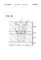
- FIG. 16depicts a cross-section of a vial level aluminum/copper dual damascene interconnect having a first insulating layer containing a conductive metal plug, a second insulating layer overlying the first insulating layer and having a first opening, where the first opening lies over at least a part of the conductive metal plug and where the first opening is overlaid with an aluminum diffusion barrier layer which is in turn overlaid with a wetting layer for aluminum and then filled with an aluminum layer, and a third insulating layer overlying the second insulating layer and having a second opening, where the second opening lies over at least a part of the aluminum layer and where the second opening is overlaid with a Ti x Al y N z barrier layer and then filled with copper.
- the present inventionprovides generally for improved methods for filling openings in silicon substrates with copper.
- One methodinvolves the use of a Ti x Al y N z barrier layer which is stable to the high temperatures required to reflow copper after PVD deposition.
- Another methodinvolves the use of an aluminum wetting layer between a barrier layer and the copper which effectively lowers the temperature at which copper reflows and therefore allows the use of typical barrier layers.
- the term “opening”refers to vias, trenches, grooves, contact holes, and the like in silicon substrates.
- the term “silicon substrate”refers to silicon structures, including silicon wafers, silicon structures in the process of fabrication, any layer on a silicon substrate which is in the process of fabrication, a semiconductor layer, including a semiconductor layer in the process of fabrication, and the like.
- the term “silicon wafer”means either the lowest layer of a semiconductor material in a wafer or a wafer having additional layers or structures formed thereon.
- fabricationmeans the process of forming patterns on a silicon structure or semiconductor structure through photolithography.
- FIG. 1shows a cross-section of an insulating layer 1 of a silicon substrate having an opening which is overlaid with a Ti x Al y N z barrier layer 2 and then filled with copper 3.
- Ti x Al x N zeach of x, y, and z is an integer such that each of Ti, Al, and N constitutes greater than 10% of the total atomic composition, wherein a composition with approximately 35-45% titanium, 5-15% aluminum, and 45-55% nitrogen is preferred, and a composition with 40% titanium, 10% aluminum, and 50% nitrogen is especially preferred.
- the Ti x Al y N z barrier layer 2is deposited by target sputtering (PVD) TiAl in a nitrogen atmosphere.
- the TiAlhas an atomic composition of approximately 75-85% titanium and 15-25% aluminum, with 80% titanium and 20% aluminum being preferred.
- the Ti x Al y N z barrier layer 2is deposited to a thickness of approximately 200 ⁇ to approximately 500 ⁇ .
- Copper 3is then deposited over the Ti x Al y N z barrier layer 2 by PVD sputter to fill the opening. Alternatively, copper 3 may be deposited by CVD, electroplating or electroless plating techniques.
- the Ti x Al y N z barrier layer 2may optionally be annealed in an oxygen atmosphere by subjecting the silicon substrate so formed to rapid thermal processing (RTP) while flowing in oxygen at a temperature of less then 700° C. for less than 5 minutes prior to the deposition of copper 3, thereby doping the Ti x Al y N z barrier layer 2 with oxygen or an oxygen species O m wherein m is greater than or equal to 1. Copper 3 is then hot deposited at a temperature of approximately 450° C. to approximately 550° C. by a PVD sputter to a thickness which is sufficient to fill the opening.
- RTPrapid thermal processing
- the copper layeris then annealed by subjecting the silicon substrate so formed to an elevated temperature in a vacuum for a period of time less than 5 minutes.
- the annealmay be carried out by flowing in gases, such as hydrogen.
- the copperis then caused to reflow at a temperature greater than about 500° C. by techniques well known to one of ordinary skill in the art.
- FIG. 2shows a cross-section of an insulating layer 1 of a silicon substrate having an opening which is overlaid with a copper diffusion barrier layer 4 which is then overlaid with aluminum wetting layer 5.
- the copper diffusion barrier layer 4may be any metal nitride and includes tantalum nitride (TaN), titanium nitride (TiN), tungsten nitride (WN) and a titanium aluminum nitride (Ti x Al y N z ) having the atomic composition described above in the description of FIG. 1 being preferred.
- the copper diffusion barrier layer 4is deposited by PVD or CVD techniques well known to one of ordinary skill in the art and is deposited to a thickness of approximately 100 ⁇ to approximately 2000 ⁇ .
- Aluminum wetting layer 5is then deposited over the copper diffusion barrier layer 4.
- the aluminum wetting layer 5is deposited using PVD or CVD techniques well known to one of ordinary skill in the art and is deposited to a thickness of approximately 50 ⁇ to approximately 500 ⁇ , with approximately 200 ⁇ being preferred.
- FIG. 3shows a cross-section of an insulating layer 1 of a silicon substrate having an opening which is overlaid with a copper diffusion barrier layer 4 which, after being overlaid with an aluminum wetting layer 5 (not shown), is then filled with copper 3, annealed, and caused to reflow as described above in the description of FIG. 1.
- the aluminum wetting layer 5is consumed thereby forming a Cu n Al alloy layer 6 wherein n is an integer from about 0.5 to about 4.
- the Cu n Al alloy layer 6has a lower melting point (i.e., 450° C.) than elemental copper (i.e., 1000° C.), thus making it easier for the copper to flow into the opening.
- total consumption of aluminum wetting layer 5may not occur upon the deposition of copper 3, annealing and reflow steps, and that some aluminum which is not in the form of a Cu n Al alloy may be present in the layer which is depicted as the Cu n Al alloy layer 6.
- FIG. 4shows a cross-section of a contact level dual damascene having a silicon substrate 10 having a first insulating layer 7 having an opening and a second insulating layer 9 having an opening, wherein the opening in the second insulating layer 9 lies over at least a part of the opening in the first insulating layer 7 thereby forming an opening through the first and second insulating layers and where the opening is overlaid with a refractory metal layer 13 which is in turn overlayed with a Ti x Al y N z barrier layer 2, the Ti x Al y N z barrier layer 2 optionally doped with oxygen or an oxygen species O m wherein m is as previously defined, and then filled with copper 3, annealed, and caused to reflow as described above in the description of FIG.
- a refractory metal silicide MSi x 11Upon overlaying the opening with a refractory metal layer 13, at least a portion of the silicon substrate 10 lying directly below the refractory metal 13 consists at least in part of a refractory metal silicide MSi x 11, wherein x is an integer from about 0.5 to about 4.
- the refractory metal silicide MSi x 11provides for a low resistance contact between the interconnect and the silicon substrate 10.
- the refractory metal layer 13may be any refractory metal and includes Ti, Ta, W, Co, Ni and TiAl.
- the refractory metal layer 13is deposited by PVD or CVD techniques as are well known to one of ordinary skill in the art, PVD deposition being preferred, and is deposited to a thickness of approximately 100 ⁇ to approximately 800 ⁇ , with approximately 300 ⁇ being preferred.
- the fabrication of a contact level dual damascene as shown in FIG. 4may be accomplished by using patterning, deposition and planarization techniques and using materials well known to one of ordinary skill in the art.
- a suitable first insulating layer 7is borophosphorous silicate glass and a suitable second insulating layer 9 is silicon oxide which may be deposited from tetraethyl orthosilicate with plasma-assistance (PETEOS).
- FIG. 5shows a cross-section of a contact level dual damascene prior to filling with copper, having a silicon substrate 10 having a first insulating layer 7 having an opening and a second insulating layer 9 having an opening, wherein the opening in the second insulating layer 9 lies over at least a part of the opening in the first insulating layer 7 thereby forming an opening through the first and second insulating layers and where the opening is overlaid with a refractory metal layer 13 which is in turn overlaid with a copper diffusion barrier layer 4 which is in turn overlaid with an aluminum wetting layer 5.
- a refractory metal layer 13as described in FIG.
- At least a portion of the silicon substrate 10 lying directly below the refractory metal 13consists at least in part of a refractory metal silicide MSi x 11 as described in FIG. 4.
- the fabrication of a contact level dual damascene as shown in FIG. 5may be as described in FIG. 4.
- FIG. 6shows a cross-section of a contact level dual damascene having a silicon substrate 10 having a first insulating layer 7 having an opening and a second insulating layer 9 having an opening, wherein the opening in the second insulating layer 9 lies over at least a part of the opening in the first insulating layer 7 thereby forming an opening through the first and second insulating layers, and where the opening is overlaid with a refractory metal layer 13 which is in turn overlaid with a copper diffusion barrier layer 4 which, after being overlaid with an aluminum wetting layer 5 (not shown), is then filled with copper 3, annealed, and caused to reflow as described above in the description of FIG. 1.
- the aluminum wetting layer 5is consumed thereby forming a Cu n Al alloy layer 6 as described previously in FIG. 3.
- a refractory metal layer 13as described in FIG. 4
- at least a portion of the silicon substrate 10 lying directly below the refractory metal 13consists at least in part of a refractory metal silicide MSi x 11 as described in FIG. 4.
- the fabrication of a contact level dual damascene as shown in FIG. 6may be accomplished as described in FIG. 4.
- FIG. 7shows a cross-section of an interconnect of the present invention having a first insulating layer 7 containing a conductive metal plug 8 and a second insulating layer 9 having an opening overlying the first insulating layer 7 where the opening lies over at least a part of the conductive metal plug 8 and where the opening is overlaid with a Ti x Al y N z barrier layer 2, the Ti x Al y N z barrier layer 2 optionally doped with oxygen as described previously in FIG. 1, and then filled with copper 3, annealed, and caused to reflow as is described above in the description of FIG. 1.
- the fabrication of silicon substrate to form an interconnectas shown in FIG.
- a suitable first insulating layer 7is borophosphorous silicate glass and a suitable second insulating layer 9 is silicon oxide which may be deposited from tetraethyl orthosilicate (TEOS).
- TEOStetraethyl orthosilicate
- An example of a conductive metal plug 8is a tungsten plug.
- FIG. 8depicts a cross-section of an interconnect having a first insulating layer 7 containing a conductive metal plug 8 and a second insulating layer 9 having an opening overlying the first insulating layer 7 where the opening lies over at least a part of the conductive metal plug 8 and where the opening is first overlaid with a copper diffusion barrier layer 4 and which is in turn overlaid with an aluminum wetting layer (not shown) and then filled with copper, annealed, and caused to reflow as described above in the embodiments depicted in FIG. 2 and FIG. 3, showing the formation of a Cu n Al alloy 6 as is described in the embodiment depicted in FIG. 3.
- the fabrication of silicon substrate to form an interconnect as shown in FIG. 8may be accomplished by using depositing, patterning, and planarization techniques and using materials well known to one of ordinary skill in the art and as described above in the embodiments depicted in FIG. 7.
- FIG. 9shows a cross-section of a via level copper/copper dual damascene interconnect of the present invention having a first insulating layer 7 containing a conductive metal plug 8, a second insulating layer 9 having a first opening overlying the first insulating layer 7 where the first opening lies over at least a part of the conductive metal plug 8 and where the first opening is overlaid with a first Ti x Al y N z barrier layer 2, the first Ti x Al y N z barrier layer 2 optionally doped with oxygen as described previously in FIG. 1, and then filled with copper 15 as described above in the description of FIG.
- a third insulating layer 14having a second opening overlying the second insulating layer 9 where the second opening lies over at least a part of the copper 15 and where the second opening is overlaid with a second Ti x Al y N z barrier layer 2b, the second Ti x Al y N z barrier layer 2b being optionally doped with oxygen as described previously in FIG. 1, and then filled with copper 3, annealed, and caused to reflow as described above in the description of FIG. 1.
- CMPchemical mechanical planarization
- a suitable first insulating layer 7is borophosphorous silicate glass
- a suitable second insulating layer 9is silicon oxide which may be deposited from tetraethyl orthosilicate (TEOS), deposited to a thickness of approximately 1000 ⁇ to approximately 1.5 ⁇ m
- a suitable third insulating layer 14is silicon oxide which may be deposited from tetraethyl orthosilicate (TEOS), deposited to a thickness of approximately 400 ⁇ to approximately 2 ⁇ m.
- FIG. 10shows a cross-section of a via level copper/copper dual damascene interconnect of the present invention having a first insulating layer 7 containing a conductive metal plug 8, a second insulating layer 9 having a first opening overlying the first insulating layer 7 where the first opening lies over at least a part of the conductive metal plug 8 and where the first opening is overlaid with a copper diffusion barrier layer 4 and which is in turn overlaid with an aluminum wetting layer (not shown) and then filled with copper 15 as described above in the embodiments depicted in FIG. 3 but without the annealing and reflow steps, showing the formation of a Cu n Al alloy 6 as is described in the embodiment depicted in FIG.
- the fabrication of silicon substrate to form a via level copper/copper dual damascene interconnect as shown in FIG. 10may be accomplished using depositing, patterning, and planarization techniques and using material well known to one of ordinary skill in the art and as described above in FIG. 9.
- FIG. 11shows a cross-section of a via level copper/copper dual damascene interconnect of the present invention having a first insulating layer 7 containing a conductive metal plug 8, a second insulating layer 9 having a first opening overlying the first insulating layer 7 where the first opening lies over at least a part of the conductive metal plug 8 and where the first opening is overlaid with a Ti x Al y N z barrier layer 2, the Ti x Al y N z barrier layer 2 optionally doped with oxygen as described previously in FIG. 1, and then filled with copper 15 as described above in the description of FIG.
- a third insulating layer 14having a second opening overlying the second insulating layer 9 where the second opening lies over at least a part of the copper 15 and where the second opening is overlaid with a copper diffusion barrier layer 4 and which is in turn overlaid with an aluminum wetting layer (not shown) and then filled with copper 3, annealed, and caused to reflow as described above in the embodiments depicted in FIG. 1, showing the formation of a Cu n Al alloy 6 as is described in the embodiment depicted in FIG. 3.
- the fabrication of silicon substrate to form a via level copper/copper dual damascene interconnect as shown in FIG. 11may be accomplished by using depositing, patterning, and planarization techniques and using materials well known to one of ordinary skill in the art and as described above in the embodiments depicted in FIG. 9.
- FIG. 12shows a cross-section of a via level copper/copper dual damascene interconnect of the present invention having a first insulating layer 7 containing a conductive metal plug 8, a second insulating layer 9 having a first opening overlying the first insulating layer 7 where the first opening lies over at least a part of the conductive metal plug 8 and where the first opening is overlaid with a first copper diffusion barrier layer 4a and which is in turn overlaid with an first aluminum wetting layer (not shown) and then filled with copper 15 as described above in the embodiments depicted in FIG. 2 but without the annealing and reflow steps, showing the formation of a first Cu n Al alloy 6a as is described in the embodiment depicted in FIG.
- a third insulating layer 14having a second opening overlying the second insulating layer 9 where the second opening lies over at least a part of the copper 15 and where the second opening is overlaid with a second copper diffusion barrier layer 4b and which is in turn overlaid with a second aluminum wetting layer (not shown) and then filled with copper 3, annealed, and caused to reflow as described above in the embodiments depicted in FIG. 1, showing the formation of a second Cu n Al alloy 6b as is described in the embodiment depicted in FIG. 3.
- the fabrication of silicon substrate to form a via level copper/copper dual damascene interconnect as shown in FIG. 12may be accomplished by using depositing, patterning, and planarization techniques and using materials well known to one of ordinary skill in the art and as described above in the embodiments depicted in FIG. 9.
- FIG. 13shows a cross-section of a via level aluminum/copper dual damascene interconnect of the present invention having a first insulating layer 7 containing a conductive metal plug 8, a second insulating layer 9 having a first opening overlying the first insulating layer 7 where the first opening lies over at least a part of the conductive metal plug 8 and where the first opening is overlaid with a wetting layer for aluminum 17 and then filled with aluminum 16, and a third insulating layer 14 having a second opening overlying the second insulating layer 9 where the second opening lies over at least a part of the aluminum 16 and where the second opening is overlaid with a copper diffusion barrier layer 4 and which is in turn overlaid with an aluminum wetting layer (not shown) and then filled with copper 3, annealed, and caused to reflow as described above in the embodiments depicted in FIG.
- the wetting layer for aluminum 17is selected from the group consisting of titanium and titanium nitride and is deposited by PVD techniques well known to one of ordinary skill in the art to a thickness of approximately 100 ⁇ to approximately 800 ⁇ , with approximately 300 ⁇ being preferred.
- Aluminum 16is then deposited using techniques and procedures well known to one of ordinary skill in the art to a thickness sufficient to fill the first opening.
- CMPchemical mechanical planarization
- the fabrication of silicon substrate to form a via level aluminum/copper dual damascene interconnect as shown in FIG. 13may be accomplished by using depositing, patterning, and planarization techniques and using materials well known to one of ordinary skill in the art and as described above in the embodiments depicted in FIG. 9.
- FIG. 14shows a cross-section of a via level aluminum/copper dual damascene interconnect of the present invention having a first insulating layer 7 containing a conductive metal plug 8, a second insulating layer 9 having a first opening overlying the first insulating layer 7 where the first opening lies over at least a part of the conductive metal plug 8 and where the first opening is overlaid with an aluminum diffusion barrier layer 18 which is then overlaid with a wetting layer for aluminum 19 and then filled with aluminum 16, and a third insulating layer 14 having a second opening overlying the second insulating layer 9 where the second opening lies over at least a part of the aluminum 16 and where the second opening is overlaid with a copper diffusion barrier layer 4 and which is in turn overlaid with an aluminum wetting layer (not shown) and then filled with copper 3, annealed, and caused to reflow as described above in the embodiments depicted in FIG.
- the aluminum diffusion barrier layer 18is typically titanium or titanium nitride and is deposited by PVD or CVD techniques well known to one of ordinary skill in the art and is deposited to a thickness of approximately 100 ⁇ to approximately 800 ⁇ , with approximately 300 ⁇ being preferred.
- the wetting layer for aluminum 19typically titanium or titanium nitride and is deposited by PVD techniques well known to one of ordinary skill in the art and is deposited to a thickness of approximately 100 ⁇ to approximately 800 ⁇ , with approximately 300 ⁇ being preferred.
- the wetting layer for aluminum 19is titanium nitride and the aluminum diffusion barrier layer 18 is titanium, in addition to acting as a diffusion barrier for aluminum, the titanium will also act to increase the electrical contact to the conductive metal plug 8.
- Aluminum 16is then deposited as described above in FIG. 13.
- the fabrication of silicon substrate to form a via level aluminum/copper dual damascene interconnect as shown in FIG. 14may be accomplished by using deposition, patterning, and planarization techniques and using materials well known to one of ordinary skill in the art and as described above in the embodiments depicted in FIG. 9.
- FIG. 15shows a cross-section of a via level aluminum/copper dual damascene interconnect of the present invention having a first insulating layer 7 containing a conductive metal plug 8, a second insulating layer 9 having a first opening overlying the first insulating layer 7 where the first opening lies over at least a part of the conductive metal plug 8 and where the first opening is overlaid with a wetting layer for aluminum 17 and then filled with aluminum 16 and a third insulating layer 14 having a second opening overlying the second insulating layer 9 where the second opening lies over at least a part of the aluminum 16 and where the second opening is overlaid with a Ti x Al y N z barrier layer 2, the Ti x Al y N z barrier layer 2 optionally doped with oxygen as described previously in FIG.
- the wetting layer for aluminum 17is as described and as deposited as described in FIG. 13.
- Aluminum 16is deposited as described above in FIG. 13.
- the fabrication of silicon substrate to form a via level aluminum/copper dual damascene interconnect as shown in FIG. 14may be accomplished by using depositing, patterning, and planarization techniques and using materials well known to one of ordinary skill in the art and as described above in the embodiments depicted in FIG. 9.
- FIG. 16shows a cross-section of a via level aluminum/copper dual damascene interconnect of the present invention having a first insulating layer 7 containing a conductive metal plug 8, a second insulating layer 9 having a first opening overlying the first insulating layer 7 where the first opening lies over at least a part of the conductive metal plug 8 and where the first opening is overlaid with an aluminum diffusion barrier layer 18 which is then overlaid with a wetting layer for aluminum 19 and then filled with aluminum 16, which is reflowed during deposition, and a third insulating layer 14 having a second opening overlying the second insulating layer 9 where the second opening lies over at least a part of the aluminum 16 and where the second opening is overlaid with a Ti x Al y N z barrier layer 2, the Ti x Al y z barrier layer 2 optionally doped with oxygen as described previously in FIG.
- the aluminum diffusion barrier layer 18, wetting layer for aluminum 19, and aluminum 16are deposited as described and as deposited as in FIG. 14.
- the fabrication of silicon substrate to form a via level aluminum/copper dual damascene interconnect as shown in FIG. 14may be accomplished by using depositing, patterning, and planarization techniques and using materials well known to one of ordinary skill in the art and as described above in the embodiments depicted in FIG. 9.
Landscapes
- Engineering & Computer Science (AREA)
- Physics & Mathematics (AREA)
- Condensed Matter Physics & Semiconductors (AREA)
- General Physics & Mathematics (AREA)
- Computer Hardware Design (AREA)
- Microelectronics & Electronic Packaging (AREA)
- Power Engineering (AREA)
- Manufacturing & Machinery (AREA)
- Plasma & Fusion (AREA)
- Internal Circuitry In Semiconductor Integrated Circuit Devices (AREA)
Abstract
Description
Claims (61)
Priority Applications (2)
| Application Number | Priority Date | Filing Date | Title |
|---|---|---|---|
| US09/038,221US5939788A (en) | 1998-03-11 | 1998-03-11 | Copper diffusion barrier, aluminum wetting layer and improved methods for filling openings in silicon substrates with cooper |
| US09/351,074US6204179B1 (en) | 1998-03-11 | 1999-07-09 | Copper diffusion barrier, aluminum wetting layer and improved methods for filling openings in silicon substrates with copper |
Applications Claiming Priority (1)
| Application Number | Priority Date | Filing Date | Title |
|---|---|---|---|
| US09/038,221US5939788A (en) | 1998-03-11 | 1998-03-11 | Copper diffusion barrier, aluminum wetting layer and improved methods for filling openings in silicon substrates with cooper |
Related Child Applications (1)
| Application Number | Title | Priority Date | Filing Date |
|---|---|---|---|
| US09/351,074ContinuationUS6204179B1 (en) | 1998-03-11 | 1999-07-09 | Copper diffusion barrier, aluminum wetting layer and improved methods for filling openings in silicon substrates with copper |
Publications (1)
| Publication Number | Publication Date |
|---|---|
| US5939788Atrue US5939788A (en) | 1999-08-17 |
Family
ID=21898714
Family Applications (2)
| Application Number | Title | Priority Date | Filing Date |
|---|---|---|---|
| US09/038,221Expired - LifetimeUS5939788A (en) | 1998-03-11 | 1998-03-11 | Copper diffusion barrier, aluminum wetting layer and improved methods for filling openings in silicon substrates with cooper |
| US09/351,074Expired - LifetimeUS6204179B1 (en) | 1998-03-11 | 1999-07-09 | Copper diffusion barrier, aluminum wetting layer and improved methods for filling openings in silicon substrates with copper |
Family Applications After (1)
| Application Number | Title | Priority Date | Filing Date |
|---|---|---|---|
| US09/351,074Expired - LifetimeUS6204179B1 (en) | 1998-03-11 | 1999-07-09 | Copper diffusion barrier, aluminum wetting layer and improved methods for filling openings in silicon substrates with copper |
Country Status (1)
| Country | Link |
|---|---|
| US (2) | US5939788A (en) |
Cited By (89)
| Publication number | Priority date | Publication date | Assignee | Title |
|---|---|---|---|---|
| US6008114A (en)* | 1998-06-08 | 1999-12-28 | United Microelectronics Corp. | Method of forming dual damascene structure |
| US6016011A (en)* | 1999-04-27 | 2000-01-18 | Hewlett-Packard Company | Method and apparatus for a dual-inlaid damascene contact to sensor |
| US6040243A (en)* | 1999-09-20 | 2000-03-21 | Chartered Semiconductor Manufacturing Ltd. | Method to form copper damascene interconnects using a reverse barrier metal scheme to eliminate copper diffusion |
| US6051496A (en)* | 1998-09-17 | 2000-04-18 | Taiwan Semiconductor Manufacturing Company | Use of stop layer for chemical mechanical polishing of CU damascene |
| US6054771A (en)* | 1997-01-31 | 2000-04-25 | Nec Corporation | Interconnection system in a semiconductor device |
| GB2345791A (en)* | 1999-01-12 | 2000-07-19 | Nec Corp | Interconnect having intermediate film functioning as etch stop and barrier film |
| US6096649A (en)* | 1999-10-25 | 2000-08-01 | Taiwan Semiconductor Manufacturing Company | Top metal and passivation procedures for copper damascene structures |
| US6111619A (en)* | 1999-05-27 | 2000-08-29 | Sharp Laboratories Of America, Inc. | Method of forming polycrystalline silicon TFTs with TiN/Cu/TiN interconnections for a liquid crystal display pixel array |
| US6110819A (en)* | 1994-10-31 | 2000-08-29 | International Business Machines Corporation | Interconnect structure using Al2 Cu for an integrated circuit chip |
| US6114243A (en)* | 1999-11-15 | 2000-09-05 | Chartered Semiconductor Manufacturing Ltd | Method to avoid copper contamination on the sidewall of a via or a dual damascene structure |
| US6127732A (en)* | 1996-04-12 | 2000-10-03 | Micron Technology, Inc. | Semiconductor device having high aspect ratio contacts |
| US6127258A (en)* | 1998-06-25 | 2000-10-03 | Motorola Inc. | Method for forming a semiconductor device |
| US6157081A (en)* | 1999-03-10 | 2000-12-05 | Advanced Micro Devices, Inc. | High-reliability damascene interconnect formation for semiconductor fabrication |
| US6156655A (en)* | 1999-09-30 | 2000-12-05 | United Microelectronics Corp. | Retardation layer for preventing diffusion of metal layer and fabrication method thereof |
| US6177347B1 (en)* | 1999-07-02 | 2001-01-23 | Taiwan Semiconductor Manufacturing Company | In-situ cleaning process for Cu metallization |
| US6184137B1 (en)* | 1998-11-25 | 2001-02-06 | Applied Materials, Inc. | Structure and method for improving low temperature copper reflow in semiconductor features |
| US6187667B1 (en)* | 1998-06-17 | 2001-02-13 | Cypress Semiconductor Corp. | Method of forming metal layer(s) and/or antireflective coating layer(s) on an integrated circuit |
| EP1081752A1 (en)* | 1999-09-03 | 2001-03-07 | Chartered Semiconductor Manufacturing Pte Ltd. | Method to form copper interconnects by adding an aluminium layer to the diffusion barrier |
| US6207545B1 (en)* | 1998-11-30 | 2001-03-27 | Taiwan Semiconductor Manufacturing Corporation | Method for forming a T-shaped plug having increased contact area |
| US6218302B1 (en)* | 1998-07-21 | 2001-04-17 | Motorola Inc. | Method for forming a semiconductor device |
| US6235632B1 (en)* | 1998-01-13 | 2001-05-22 | Advanced Micro Devices, Inc. | Tungsten plug formation |
| US6274484B1 (en) | 2000-03-17 | 2001-08-14 | Taiwan Semiconductor Manufacturing Company | Fabrication process for low resistivity tungsten layer with good adhesion to insulator layers |
| US6297154B1 (en)* | 1998-08-28 | 2001-10-02 | Agere System Guardian Corp. | Process for semiconductor device fabrication having copper interconnects |
| US6316359B1 (en)* | 1998-02-12 | 2001-11-13 | Motorola Inc. | Interconnect structure in a semiconductor device and method of formation |
| US6329281B1 (en) | 1999-12-03 | 2001-12-11 | Agere Systems Guardian Corp. | Methods for fabricating a multilevel interconnection for an integrated circuit device utilizing a selective overlayer |
| US20010054765A1 (en)* | 2000-06-20 | 2001-12-27 | Nec Corporation | Semiconductor device and method and apparatus for manufacturing the same |
| WO2002014576A1 (en)* | 2000-08-15 | 2002-02-21 | Honeywell International Inc. | Sputtering target |
| US20020022363A1 (en)* | 1998-02-04 | 2002-02-21 | Thomas L. Ritzdorf | Method for filling recessed micro-structures with metallization in the production of a microelectronic device |
| US6368967B1 (en)* | 2000-05-04 | 2002-04-09 | Advanced Micro Devices, Inc. | Method to control mechanical stress of copper interconnect line using post-plating copper anneal |
| US6373137B1 (en) | 2000-03-21 | 2002-04-16 | Micron Technology, Inc. | Copper interconnect for an integrated circuit and methods for its fabrication |
| US6380625B2 (en) | 1999-01-13 | 2002-04-30 | Advanced Micro Devices, Inc. | Semiconductor interconnect barrier and manufacturing method thereof |
| US6400031B1 (en)* | 1998-06-11 | 2002-06-04 | Oki Electric Industry Co., Ltd. | Semiconductor device having damascene interconnection structure that prevents void formation between interconnections |
| US20020074233A1 (en)* | 1998-02-04 | 2002-06-20 | Semitool, Inc. | Method and apparatus for low temperature annealing of metallization micro-structures in the production of a microelectronic device |
| US6413858B1 (en) | 1999-08-27 | 2002-07-02 | Micron Technology, Inc. | Barrier and electroplating seed layer |
| US6417116B2 (en)* | 1998-03-24 | 2002-07-09 | Fujitsu Limited | Semiconductor device having a multilayer interconnection structure |
| US6423201B1 (en) | 2000-08-23 | 2002-07-23 | Applied Materials, Inc. | Method of improving the adhesion of copper |
| US20020100983A1 (en)* | 2001-01-31 | 2002-08-01 | Clevenger Lawrence A. | Method for producing dual damascene interconnections and structure produced thereby |
| US6475913B1 (en) | 1999-06-24 | 2002-11-05 | Hyundai Electronics Industries Co., Ltd. | Method for forming damascene type of metal wires in semiconductor devices |
| US20020168863A1 (en)* | 1999-01-27 | 2002-11-14 | Semitool, Inc. | Selective treatment of the surface of a microelectronic workpiece |
| US20020187631A1 (en)* | 2000-12-06 | 2002-12-12 | Ki-Bum Kim | Copper interconnect structure having stuffed diffusion barrier |
| US6518183B1 (en) | 2001-09-06 | 2003-02-11 | Taiwan Semiconductor Manufacturing Co., Ltd. | Hillock inhibiting method for forming a passivated copper containing conductor layer |
| US6531780B1 (en)* | 2001-06-27 | 2003-03-11 | Advanced Micro Devices, Inc. | Via formation in integrated circuit interconnects |
| US6541371B1 (en) | 1999-02-08 | 2003-04-01 | Novellus Systems, Inc. | Apparatus and method for depositing superior Ta(N)/copper thin films for barrier and seed applications in semiconductor processing |
| US6545358B2 (en)* | 1998-09-16 | 2003-04-08 | Samsung Electronics, Co., Ltd. | Integrated circuits having plugs in conductive layers therein and related methods |
| US6551483B1 (en) | 2000-02-29 | 2003-04-22 | Novellus Systems, Inc. | Method for potential controlled electroplating of fine patterns on semiconductor wafers |
| US6562712B2 (en) | 2001-07-03 | 2003-05-13 | Taiwan Semiconductor Manufacturing Co., Ltd | Multi-step planarizing method for forming a patterned thermally extrudable material layer |
| US20030111012A1 (en)* | 1999-12-24 | 2003-06-19 | Murata Manufacturing Co., Ltd. | Method for forming a thin film and a thin film forming apparatus therefor |
| US20030132123A1 (en)* | 2000-10-24 | 2003-07-17 | Turner Stephen P. | Methods of forming titanium-based and zirconium-based mixed-metal materials |
| US20030151079A1 (en)* | 2000-11-15 | 2003-08-14 | Jones Robert E. | Self-aligned magnetic clad write line and its method of formation |
| US6610596B1 (en)* | 1999-09-15 | 2003-08-26 | Samsung Electronics Co., Ltd. | Method of forming metal interconnection using plating and semiconductor device manufactured by the method |
| US6624067B2 (en) | 2001-02-13 | 2003-09-23 | Bae Systems And Information And Electronic Systems Integration Inc. | Process for removing a silicon-containing material through use of a byproduct generated during formation of a diffusion barrier layer |
| US6649511B1 (en)* | 2000-11-06 | 2003-11-18 | Advanced Micro Devices, Inc. | Method of manufacturing a seed layer with annealed region for integrated circuit interconnects |
| US20030224611A1 (en)* | 1999-03-12 | 2003-12-04 | Kabushiki Kaisha Toshiba | Manufacturing method of semiconductor devices by using dry etching technology |
| US20030227068A1 (en)* | 2001-05-31 | 2003-12-11 | Jianxing Li | Sputtering target |
| US20040041273A1 (en)* | 2002-08-30 | 2004-03-04 | Chia-Hong Jan | Structure and manufacturing process of localized shunt to reduce electromigration failure of copper dual damascene process |
| US20040052930A1 (en)* | 2000-04-27 | 2004-03-18 | Bulent Basol | Conductive structure fabrication process using novel layered structure and conductive structure fabricated thereby for use in multi-level metallization |
| US20040123920A1 (en)* | 2002-10-08 | 2004-07-01 | Thomas Michael E. | Homogenous solid solution alloys for sputter-deposited thin films |
| US20040132282A1 (en)* | 2002-03-27 | 2004-07-08 | Qing-Tang Jiang | Copper transition layer for improving copper interconnection reliability |
| US20040175926A1 (en)* | 2003-03-07 | 2004-09-09 | Advanced Micro Devices, Inc. | Method for manufacturing a semiconductor component having a barrier-lined opening |
| US6793796B2 (en) | 1998-10-26 | 2004-09-21 | Novellus Systems, Inc. | Electroplating process for avoiding defects in metal features of integrated circuit devices |
| US20040219783A1 (en)* | 2001-07-09 | 2004-11-04 | Micron Technology, Inc. | Copper dual damascene interconnect technology |
| US6815342B1 (en)* | 2001-11-27 | 2004-11-09 | Lsi Logic Corporation | Low resistance metal interconnect lines and a process for fabricating them |
| US6841477B1 (en)* | 1999-08-27 | 2005-01-11 | Fujitsu Limited | Metal interconnection, semiconductor device, method for forming metal interconnection and method for fabricating semiconductor device |
| US20050167844A1 (en)* | 2004-02-03 | 2005-08-04 | Nec Electronics Corporation | Semiconductor device |
| US20050196950A1 (en)* | 2001-12-13 | 2005-09-08 | Werner Steinhogl | Method of producing layered assembly and a layered assembly |
| US6946065B1 (en) | 1998-10-26 | 2005-09-20 | Novellus Systems, Inc. | Process for electroplating metal into microscopic recessed features |
| US20070070621A1 (en)* | 2002-09-23 | 2007-03-29 | Matrix Railway Corporation | Led lighting apparatus |
| US7211175B1 (en) | 2000-02-29 | 2007-05-01 | Novellus Systems, Inc. | Method and apparatus for potential controlled electroplating of fine patterns on semiconductor wafers |
| US20070114671A1 (en)* | 2005-11-18 | 2007-05-24 | Yu-Hao Hsu | Interconnect structure and fabricating method thereof |
| US20070164442A1 (en)* | 2000-04-11 | 2007-07-19 | Micron Technology, Inc. | Use of AIN as cooper passivation layer and thermal conductor |
| US20070194448A1 (en)* | 2003-12-31 | 2007-08-23 | Se-Yeul Bae | Semiconductor interconnection line and method of forming the same |
| US20080081444A1 (en)* | 2006-09-28 | 2008-04-03 | Promos Technologies Inc. | Method for forming silicide layer on a silicon surface and its use |
| US7399713B2 (en) | 1998-03-13 | 2008-07-15 | Semitool, Inc. | Selective treatment of microelectric workpiece surfaces |
| US20080315174A1 (en)* | 2007-06-20 | 2008-12-25 | Samsung Electronics Co., Ltd. | Variable resistance non-volatile memory cells and methods of fabricating same |
| US20090160055A1 (en)* | 2007-12-19 | 2009-06-25 | Lavoie Adrien R | IC solder reflow method and materials |
| US20110063835A1 (en)* | 2002-09-23 | 2011-03-17 | Nelson Rivas | Led lighting apparatus |
| US20140091467A1 (en)* | 2012-09-28 | 2014-04-03 | Christopher J. Jezewski | Forming barrier walls, capping, or alloys /compounds within metal lines |
| US8779596B2 (en) | 2000-01-18 | 2014-07-15 | Micron Technology, Inc. | Structures and methods to enhance copper metallization |
| US20140264872A1 (en)* | 2013-03-13 | 2014-09-18 | Taiwan Semiconductor Manufacturing Company, Ltd. | Metal Capping Layer for Interconnect Applications |
| US8936702B2 (en) | 2006-03-07 | 2015-01-20 | Micron Technology, Inc. | System and method for sputtering a tensile silicon nitride film |
| US9028666B2 (en) | 2011-05-17 | 2015-05-12 | Novellus Systems, Inc. | Wetting wave front control for reduced air entrapment during wafer entry into electroplating bath |
| US9355851B2 (en) | 2011-11-30 | 2016-05-31 | Samsung Electronics Co., Ltd. | Semiconductor devices and methods of manufacturing the same |
| US9385035B2 (en) | 2010-05-24 | 2016-07-05 | Novellus Systems, Inc. | Current ramping and current pulsing entry of substrates for electroplating |
| US10011917B2 (en) | 2008-11-07 | 2018-07-03 | Lam Research Corporation | Control of current density in an electroplating apparatus |
| USRE47630E1 (en)* | 2012-10-10 | 2019-10-01 | Globalfoundries Inc. | Semiconductor device having a self-forming barrier layer at via bottom |
| CN111613571A (en)* | 2019-02-22 | 2020-09-01 | 上海磁宇信息科技有限公司 | Method for manufacturing magnetic random access memory unit array |
| US11225727B2 (en) | 2008-11-07 | 2022-01-18 | Lam Research Corporation | Control of current density in an electroplating apparatus |
| US11664271B2 (en) | 2019-05-02 | 2023-05-30 | International Business Machines Corporation | Dual damascene with short liner |
| US20240266282A1 (en)* | 2018-08-13 | 2024-08-08 | Taiwan Semiconductor Manufacturing Co., Ltd. | Semiconductor device with source/drain via |
Families Citing this family (27)
| Publication number | Priority date | Publication date | Assignee | Title |
|---|---|---|---|---|
| US6475912B1 (en) | 1998-06-01 | 2002-11-05 | Matsushita Electric Industrial Co., Ltd. | Semiconductor device and method and apparatus for fabricating the same while minimizing operating failures and optimizing yield |
| US6982226B1 (en)* | 1998-06-05 | 2006-01-03 | Agere Systems Inc. | Method of fabricating a contact with a post contact plug anneal |
| US6221758B1 (en)* | 1999-01-04 | 2001-04-24 | Taiwan Semiconductor Manufacturing Company | Effective diffusion barrier process and device manufactured thereby |
| TW400619B (en)* | 1999-03-05 | 2000-08-01 | United Microelectronics Corp | The manufacture method of dual damascene structure |
| JP3519632B2 (en)* | 1999-03-11 | 2004-04-19 | 株式会社東芝 | Method for manufacturing semiconductor device |
| US6383917B1 (en)* | 1999-10-21 | 2002-05-07 | Intel Corporation | Method for making integrated circuits |
| US6384448B1 (en) | 2000-02-28 | 2002-05-07 | Micron Technology, Inc. | P-channel dynamic flash memory cells with ultrathin tunnel oxides |
| US6639835B2 (en) | 2000-02-29 | 2003-10-28 | Micron Technology, Inc. | Static NVRAM with ultra thin tunnel oxides |
| US6777327B2 (en)* | 2001-03-28 | 2004-08-17 | Sharp Laboratories Of America, Inc. | Method of barrier metal surface treatment prior to Cu deposition to improve adhesion and trench filling characteristics |
| KR100463178B1 (en)* | 2002-04-19 | 2004-12-23 | 아남반도체 주식회사 | Formation method of stacking structure of metal line in semiconductor device |
| US7485577B2 (en)* | 2003-04-18 | 2009-02-03 | Dongbuanam Semiconductor, Inc. | Method of forming metal line stacking structure in semiconductor device |
| US6979642B1 (en)* | 2002-07-31 | 2005-12-27 | Advanced Micro Devices, Inc. | Method of self-annealing conductive lines that separates grain size effects from alloy mobility |
| US20050006770A1 (en)* | 2003-07-08 | 2005-01-13 | Valeriy Sukharev | Copper-low-K dual damascene interconnect with improved reliability |
| US20050266679A1 (en)* | 2004-05-26 | 2005-12-01 | Jing-Cheng Lin | Barrier structure for semiconductor devices |
| US20050263891A1 (en)* | 2004-05-28 | 2005-12-01 | Bih-Huey Lee | Diffusion barrier for damascene structures |
| US7087521B2 (en)* | 2004-11-19 | 2006-08-08 | Intel Corporation | Forming an intermediate layer in interconnect joints and structures formed thereby |
| US7193327B2 (en)* | 2005-01-25 | 2007-03-20 | Taiwan Semiconductor Manufacturing Company, Ltd. | Barrier structure for semiconductor devices |
| US8308053B2 (en)* | 2005-08-31 | 2012-11-13 | Micron Technology, Inc. | Microfeature workpieces having alloyed conductive structures, and associated methods |
| US20070257366A1 (en)* | 2006-05-03 | 2007-11-08 | Taiwan Semiconductor Manufacturing Company, Ltd. | Barrier layer for semiconductor interconnect structure |
| DE102007046851B4 (en)* | 2007-09-29 | 2019-01-10 | Globalfoundries Dresden Module One Limited Liability Company & Co. Kg | Semiconductor structure with an electrically conductive structure element and method for forming a semiconductor structure |
| US20130075831A1 (en)* | 2011-09-24 | 2013-03-28 | Taiwan Semiconductor Manufacturing Company, Ltd. | Metal gate stack having tialn blocking/wetting layer |
| US8497202B1 (en)* | 2012-02-21 | 2013-07-30 | International Business Machines Corporation | Interconnect structures and methods of manufacturing of interconnect structures |
| US9646876B2 (en)* | 2015-02-27 | 2017-05-09 | Applied Materials, Inc. | Aluminum nitride barrier layer |
| US9966308B2 (en) | 2016-10-04 | 2018-05-08 | International Business Machines Corporation | Semiconductor device and method of forming the semiconductor device |
| US9960078B1 (en) | 2017-03-23 | 2018-05-01 | International Business Machines Corporation | Reflow interconnect using Ru |
| US10438846B2 (en) | 2017-11-28 | 2019-10-08 | Taiwan Semiconductor Manufacturing Co., Ltd. | Physical vapor deposition process for semiconductor interconnection structures |
| US10541199B2 (en)* | 2017-11-29 | 2020-01-21 | International Business Machines Corporation | BEOL integration with advanced interconnects |
Citations (22)
| Publication number | Priority date | Publication date | Assignee | Title |
|---|---|---|---|---|
| US4985750A (en)* | 1986-09-17 | 1991-01-15 | Fujitsu Limited | Semiconductor device using copper metallization |
| US5231306A (en)* | 1992-01-31 | 1993-07-27 | Micron Technology, Inc. | Titanium/aluminum/nitrogen material for semiconductor devices |
| US5243222A (en)* | 1991-04-05 | 1993-09-07 | International Business Machines Corporation | Copper alloy metallurgies for VLSI interconnection structures |
| US5371042A (en)* | 1992-06-16 | 1994-12-06 | Applied Materials, Inc. | Method of filling contacts in semiconductor devices |
| US5380678A (en)* | 1991-03-12 | 1995-01-10 | Yu; Chang | Bilayer barrier metal method for obtaining 100% step-coverage in contact vias without junction degradation |
| US5527739A (en)* | 1993-12-23 | 1996-06-18 | Motorola, Inc. | Process for fabricating a semiconductor device having an improved metal interconnect structure |
| US5559817A (en)* | 1994-11-23 | 1996-09-24 | Lucent Technologies Inc. | Complaint layer metallization |
| US5595937A (en)* | 1995-04-13 | 1997-01-21 | Nec Corporation | Method for fabricating semiconductor device with interconnections buried in trenches |
| US5602423A (en)* | 1994-11-01 | 1997-02-11 | Texas Instruments Incorporated | Damascene conductors with embedded pillars |
| US5602053A (en)* | 1996-04-08 | 1997-02-11 | Chartered Semidconductor Manufacturing Pte, Ltd. | Method of making a dual damascene antifuse structure |
| US5612254A (en)* | 1992-06-29 | 1997-03-18 | Intel Corporation | Methods of forming an interconnect on a semiconductor substrate |
| US5614765A (en)* | 1995-06-07 | 1997-03-25 | Advanced Micro Devices, Inc. | Self aligned via dual damascene |
| US5646448A (en)* | 1995-06-05 | 1997-07-08 | Advanced Micro Devices | Copper pellet for reducing electromigration effects associated with a conductive via in a semiconductor device |
| US5654216A (en)* | 1996-04-08 | 1997-08-05 | Chartered Semiconductor Manufacturing Pte Ltd. | Formation of a metal via structure from a composite metal layer |
| US5654232A (en)* | 1994-08-24 | 1997-08-05 | Intel Corporation | Wetting layer sidewalls to promote copper reflow into grooves |
| US5668054A (en)* | 1996-01-11 | 1997-09-16 | United Microelectronics Corporation | Process for fabricating tantalum nitride diffusion barrier for copper matallization |
| US5700716A (en)* | 1996-02-23 | 1997-12-23 | Micron Technology, Inc. | Method for forming low contact resistance contacts, vias, and plugs with diffusion barriers |
| US5708303A (en)* | 1994-09-15 | 1998-01-13 | Texas Instruments Incorporated | Semiconductor device having damascene interconnects |
| US5877076A (en)* | 1997-10-14 | 1999-03-02 | Industrial Technology Research Institute | Opposed two-layered photoresist process for dual damascene patterning |
| US5882958A (en)* | 1997-09-03 | 1999-03-16 | Wanlass; Frank M. | Damascene method for source drain definition of silicon on insulator MOS transistors |
| US5882996A (en)* | 1997-10-14 | 1999-03-16 | Industrial Technology Research Institute | Method of self-aligned dual damascene patterning using developer soluble arc interstitial layer |
| US5883006A (en)* | 1997-12-12 | 1999-03-16 | Kabushiki Kaisha Toshiba | Method for making a semiconductor device using a flowable oxide film |
Family Cites Families (4)
| Publication number | Priority date | Publication date | Assignee | Title |
|---|---|---|---|---|
| US5747360A (en)* | 1993-09-17 | 1998-05-05 | Applied Materials, Inc. | Method of metalizing a semiconductor wafer |
| KR0138307B1 (en)* | 1994-12-14 | 1998-06-01 | 김광호 | Side contact formation method of semiconductor device |
| US6387805B2 (en)* | 1997-05-08 | 2002-05-14 | Applied Materials, Inc. | Copper alloy seed layer for copper metallization |
| US5821168A (en)* | 1997-07-16 | 1998-10-13 | Motorola, Inc. | Process for forming a semiconductor device |
- 1998
- 1998-03-11USUS09/038,221patent/US5939788A/ennot_activeExpired - Lifetime
- 1999
- 1999-07-09USUS09/351,074patent/US6204179B1/ennot_activeExpired - Lifetime
Patent Citations (22)
| Publication number | Priority date | Publication date | Assignee | Title |
|---|---|---|---|---|
| US4985750A (en)* | 1986-09-17 | 1991-01-15 | Fujitsu Limited | Semiconductor device using copper metallization |
| US5380678A (en)* | 1991-03-12 | 1995-01-10 | Yu; Chang | Bilayer barrier metal method for obtaining 100% step-coverage in contact vias without junction degradation |
| US5243222A (en)* | 1991-04-05 | 1993-09-07 | International Business Machines Corporation | Copper alloy metallurgies for VLSI interconnection structures |
| US5231306A (en)* | 1992-01-31 | 1993-07-27 | Micron Technology, Inc. | Titanium/aluminum/nitrogen material for semiconductor devices |
| US5371042A (en)* | 1992-06-16 | 1994-12-06 | Applied Materials, Inc. | Method of filling contacts in semiconductor devices |
| US5612254A (en)* | 1992-06-29 | 1997-03-18 | Intel Corporation | Methods of forming an interconnect on a semiconductor substrate |
| US5527739A (en)* | 1993-12-23 | 1996-06-18 | Motorola, Inc. | Process for fabricating a semiconductor device having an improved metal interconnect structure |
| US5654232A (en)* | 1994-08-24 | 1997-08-05 | Intel Corporation | Wetting layer sidewalls to promote copper reflow into grooves |
| US5708303A (en)* | 1994-09-15 | 1998-01-13 | Texas Instruments Incorporated | Semiconductor device having damascene interconnects |
| US5602423A (en)* | 1994-11-01 | 1997-02-11 | Texas Instruments Incorporated | Damascene conductors with embedded pillars |
| US5559817A (en)* | 1994-11-23 | 1996-09-24 | Lucent Technologies Inc. | Complaint layer metallization |
| US5595937A (en)* | 1995-04-13 | 1997-01-21 | Nec Corporation | Method for fabricating semiconductor device with interconnections buried in trenches |
| US5646448A (en)* | 1995-06-05 | 1997-07-08 | Advanced Micro Devices | Copper pellet for reducing electromigration effects associated with a conductive via in a semiconductor device |
| US5614765A (en)* | 1995-06-07 | 1997-03-25 | Advanced Micro Devices, Inc. | Self aligned via dual damascene |
| US5668054A (en)* | 1996-01-11 | 1997-09-16 | United Microelectronics Corporation | Process for fabricating tantalum nitride diffusion barrier for copper matallization |
| US5700716A (en)* | 1996-02-23 | 1997-12-23 | Micron Technology, Inc. | Method for forming low contact resistance contacts, vias, and plugs with diffusion barriers |
| US5654216A (en)* | 1996-04-08 | 1997-08-05 | Chartered Semiconductor Manufacturing Pte Ltd. | Formation of a metal via structure from a composite metal layer |
| US5602053A (en)* | 1996-04-08 | 1997-02-11 | Chartered Semidconductor Manufacturing Pte, Ltd. | Method of making a dual damascene antifuse structure |
| US5882958A (en)* | 1997-09-03 | 1999-03-16 | Wanlass; Frank M. | Damascene method for source drain definition of silicon on insulator MOS transistors |
| US5877076A (en)* | 1997-10-14 | 1999-03-02 | Industrial Technology Research Institute | Opposed two-layered photoresist process for dual damascene patterning |
| US5882996A (en)* | 1997-10-14 | 1999-03-16 | Industrial Technology Research Institute | Method of self-aligned dual damascene patterning using developer soluble arc interstitial layer |
| US5883006A (en)* | 1997-12-12 | 1999-03-16 | Kabushiki Kaisha Toshiba | Method for making a semiconductor device using a flowable oxide film |
Cited By (155)
| Publication number | Priority date | Publication date | Assignee | Title |
|---|---|---|---|---|
| US6110819A (en)* | 1994-10-31 | 2000-08-29 | International Business Machines Corporation | Interconnect structure using Al2 Cu for an integrated circuit chip |
| US6127732A (en)* | 1996-04-12 | 2000-10-03 | Micron Technology, Inc. | Semiconductor device having high aspect ratio contacts |
| US6054771A (en)* | 1997-01-31 | 2000-04-25 | Nec Corporation | Interconnection system in a semiconductor device |
| US6235632B1 (en)* | 1998-01-13 | 2001-05-22 | Advanced Micro Devices, Inc. | Tungsten plug formation |
| US7144805B2 (en) | 1998-02-04 | 2006-12-05 | Semitool, Inc. | Method of submicron metallization using electrochemical deposition of recesses including a first deposition at a first current density and a second deposition at an increased current density |
| US7244677B2 (en) | 1998-02-04 | 2007-07-17 | Semitool. Inc. | Method for filling recessed micro-structures with metallization in the production of a microelectronic device |
| US7001471B2 (en) | 1998-02-04 | 2006-02-21 | Semitool, Inc. | Method and apparatus for low-temperature annealing of metallization microstructures in the production of a microelectronic device |
| US6806186B2 (en) | 1998-02-04 | 2004-10-19 | Semitool, Inc. | Submicron metallization using electrochemical deposition |
| US20020074233A1 (en)* | 1998-02-04 | 2002-06-20 | Semitool, Inc. | Method and apparatus for low temperature annealing of metallization micro-structures in the production of a microelectronic device |
| US20020022363A1 (en)* | 1998-02-04 | 2002-02-21 | Thomas L. Ritzdorf | Method for filling recessed micro-structures with metallization in the production of a microelectronic device |
| US6753251B2 (en) | 1998-02-04 | 2004-06-22 | Semitool, Inc. | Method for filling recessed micro-structures with metallization in the production of a microelectronic device |
| US7462269B2 (en) | 1998-02-04 | 2008-12-09 | Semitool, Inc. | Method for low temperature annealing of metallization micro-structures in the production of a microelectronic device |
| US6508920B1 (en) | 1998-02-04 | 2003-01-21 | Semitool, Inc. | Apparatus for low-temperature annealing of metallization microstructures in the production of a microelectronic device |
| US6316359B1 (en)* | 1998-02-12 | 2001-11-13 | Motorola Inc. | Interconnect structure in a semiconductor device and method of formation |
| US7399713B2 (en) | 1998-03-13 | 2008-07-15 | Semitool, Inc. | Selective treatment of microelectric workpiece surfaces |
| US7041586B2 (en) | 1998-03-24 | 2006-05-09 | Fujitsu Limited | Semiconductor device having a multilayer interconnection structure |
| US6417116B2 (en)* | 1998-03-24 | 2002-07-09 | Fujitsu Limited | Semiconductor device having a multilayer interconnection structure |
| US6008114A (en)* | 1998-06-08 | 1999-12-28 | United Microelectronics Corp. | Method of forming dual damascene structure |
| US20030183942A1 (en)* | 1998-06-11 | 2003-10-02 | Yusuke Harada | Semiconductor device having damascene interconnection structure that prevents void formation between interconnections |
| US20020125579A1 (en)* | 1998-06-11 | 2002-09-12 | Yusuke Harada | Semiconductor device having damascene interconnection structure that prevents void formation between interconnections |
| US20050110100A1 (en)* | 1998-06-11 | 2005-05-26 | Yusuke Harada | Semiconductor device |
| US7176577B2 (en) | 1998-06-11 | 2007-02-13 | Oki Electric Industry Co., Ltd. | Semiconductor device |
| US20050098889A1 (en)* | 1998-06-11 | 2005-05-12 | Yusuke Harada | Semiconductor device |
| US6759747B2 (en) | 1998-06-11 | 2004-07-06 | Oki Electric Industry Co., Ltd. | Semiconductor device having damascene interconnection structure that prevents void formation between interconnections |
| US6400031B1 (en)* | 1998-06-11 | 2002-06-04 | Oki Electric Industry Co., Ltd. | Semiconductor device having damascene interconnection structure that prevents void formation between interconnections |
| US7777337B2 (en) | 1998-06-11 | 2010-08-17 | Oki Semiconductor Co., Ltd. | Semiconductor device having damascene interconnection structure that prevents void formation between interconnections |
| US8786087B2 (en) | 1998-06-11 | 2014-07-22 | Oki Semiconductor Co., Ltd. | Semiconductor device having damascene interconnection structure that prevents void formation between interconnections having transparent dielectric substrate |
| US20100270675A1 (en)* | 1998-06-11 | 2010-10-28 | Oki Semiconductor Co., Ltd. | Semiconductor device having damascene interconnection structure that prevents void formation between interconnections having transparent dielectric substrate |
| US7126222B2 (en) | 1998-06-11 | 2006-10-24 | Oki Electric Industry Co., Ltd. | Semiconductor device |
| US6534398B2 (en)* | 1998-06-17 | 2003-03-18 | Cypress Semiconductor Corp. | Method of forming metal layer(s) and/or antireflective coating layer(s) on an integrated circuit |
| US6187667B1 (en)* | 1998-06-17 | 2001-02-13 | Cypress Semiconductor Corp. | Method of forming metal layer(s) and/or antireflective coating layer(s) on an integrated circuit |
| US6372665B1 (en) | 1998-06-25 | 2002-04-16 | Motorola Inc. | Method for forming a semiconductor device |
| US6127258A (en)* | 1998-06-25 | 2000-10-03 | Motorola Inc. | Method for forming a semiconductor device |
| US6218302B1 (en)* | 1998-07-21 | 2001-04-17 | Motorola Inc. | Method for forming a semiconductor device |
| US6297154B1 (en)* | 1998-08-28 | 2001-10-02 | Agere System Guardian Corp. | Process for semiconductor device fabrication having copper interconnects |
| US6545358B2 (en)* | 1998-09-16 | 2003-04-08 | Samsung Electronics, Co., Ltd. | Integrated circuits having plugs in conductive layers therein and related methods |
| US6051496A (en)* | 1998-09-17 | 2000-04-18 | Taiwan Semiconductor Manufacturing Company | Use of stop layer for chemical mechanical polishing of CU damascene |
| US8048280B2 (en) | 1998-10-26 | 2011-11-01 | Novellus Systems, Inc. | Process for electroplating metals into microscopic recessed features |
| US6793796B2 (en) | 1998-10-26 | 2004-09-21 | Novellus Systems, Inc. | Electroplating process for avoiding defects in metal features of integrated circuit devices |
| US6946065B1 (en) | 1998-10-26 | 2005-09-20 | Novellus Systems, Inc. | Process for electroplating metal into microscopic recessed features |
| US20060011483A1 (en)* | 1998-10-26 | 2006-01-19 | Novellus Systems, Inc. | Process for electroplating metals into microscopic recessed features |
| US6184137B1 (en)* | 1998-11-25 | 2001-02-06 | Applied Materials, Inc. | Structure and method for improving low temperature copper reflow in semiconductor features |
| US6352926B1 (en) | 1998-11-25 | 2002-03-05 | Applied Materials, Inc. | Structure for improving low temperature copper reflow in semiconductor features |
| US6207545B1 (en)* | 1998-11-30 | 2001-03-27 | Taiwan Semiconductor Manufacturing Corporation | Method for forming a T-shaped plug having increased contact area |
| GB2345791A (en)* | 1999-01-12 | 2000-07-19 | Nec Corp | Interconnect having intermediate film functioning as etch stop and barrier film |
| GB2345791B (en)* | 1999-01-12 | 2002-01-23 | Nec Corp | Semiconductor device and fabrication method therefor |
| US6380625B2 (en) | 1999-01-13 | 2002-04-30 | Advanced Micro Devices, Inc. | Semiconductor interconnect barrier and manufacturing method thereof |
| US20020168863A1 (en)* | 1999-01-27 | 2002-11-14 | Semitool, Inc. | Selective treatment of the surface of a microelectronic workpiece |
| US6541371B1 (en) | 1999-02-08 | 2003-04-01 | Novellus Systems, Inc. | Apparatus and method for depositing superior Ta(N)/copper thin films for barrier and seed applications in semiconductor processing |
| US6905959B1 (en) | 1999-02-08 | 2005-06-14 | Novellus Systems, Inc. | Apparatus and method for depositing superior Ta (N) copper thin films for barrier and seed applications in semiconductor processing |
| US6157081A (en)* | 1999-03-10 | 2000-12-05 | Advanced Micro Devices, Inc. | High-reliability damascene interconnect formation for semiconductor fabrication |
| US20030224611A1 (en)* | 1999-03-12 | 2003-12-04 | Kabushiki Kaisha Toshiba | Manufacturing method of semiconductor devices by using dry etching technology |
| US6016011A (en)* | 1999-04-27 | 2000-01-18 | Hewlett-Packard Company | Method and apparatus for a dual-inlaid damascene contact to sensor |
| US6111619A (en)* | 1999-05-27 | 2000-08-29 | Sharp Laboratories Of America, Inc. | Method of forming polycrystalline silicon TFTs with TiN/Cu/TiN interconnections for a liquid crystal display pixel array |
| US6475913B1 (en) | 1999-06-24 | 2002-11-05 | Hyundai Electronics Industries Co., Ltd. | Method for forming damascene type of metal wires in semiconductor devices |
| US6177347B1 (en)* | 1999-07-02 | 2001-01-23 | Taiwan Semiconductor Manufacturing Company | In-situ cleaning process for Cu metallization |
| US6545357B2 (en)* | 1999-08-27 | 2003-04-08 | Micron Technology, Inc. | Metal nitride barrier layer and electroplating seed layer with the same metal as the metal nitride layer |
| US6841477B1 (en)* | 1999-08-27 | 2005-01-11 | Fujitsu Limited | Metal interconnection, semiconductor device, method for forming metal interconnection and method for fabricating semiconductor device |
| US7041595B2 (en) | 1999-08-27 | 2006-05-09 | Micron Technology, Inc. | Method of forming a barrier seed layer with graded nitrogen composition |
| US6413858B1 (en) | 1999-08-27 | 2002-07-02 | Micron Technology, Inc. | Barrier and electroplating seed layer |
| EP1081752A1 (en)* | 1999-09-03 | 2001-03-07 | Chartered Semiconductor Manufacturing Pte Ltd. | Method to form copper interconnects by adding an aluminium layer to the diffusion barrier |
| US6740580B1 (en) | 1999-09-03 | 2004-05-25 | Chartered Semiconductor Manufacturing Ltd. | Method to form copper interconnects by adding an aluminum layer to the copper diffusion barrier |
| US6610596B1 (en)* | 1999-09-15 | 2003-08-26 | Samsung Electronics Co., Ltd. | Method of forming metal interconnection using plating and semiconductor device manufactured by the method |
| US6040243A (en)* | 1999-09-20 | 2000-03-21 | Chartered Semiconductor Manufacturing Ltd. | Method to form copper damascene interconnects using a reverse barrier metal scheme to eliminate copper diffusion |
| US6156655A (en)* | 1999-09-30 | 2000-12-05 | United Microelectronics Corp. | Retardation layer for preventing diffusion of metal layer and fabrication method thereof |
| US6096649A (en)* | 1999-10-25 | 2000-08-01 | Taiwan Semiconductor Manufacturing Company | Top metal and passivation procedures for copper damascene structures |
| US6114243A (en)* | 1999-11-15 | 2000-09-05 | Chartered Semiconductor Manufacturing Ltd | Method to avoid copper contamination on the sidewall of a via or a dual damascene structure |
| US6329281B1 (en) | 1999-12-03 | 2001-12-11 | Agere Systems Guardian Corp. | Methods for fabricating a multilevel interconnection for an integrated circuit device utilizing a selective overlayer |
| US20030111012A1 (en)* | 1999-12-24 | 2003-06-19 | Murata Manufacturing Co., Ltd. | Method for forming a thin film and a thin film forming apparatus therefor |
| US8779596B2 (en) | 2000-01-18 | 2014-07-15 | Micron Technology, Inc. | Structures and methods to enhance copper metallization |
| US6562204B1 (en) | 2000-02-29 | 2003-05-13 | Novellus Systems, Inc. | Apparatus for potential controlled electroplating of fine patterns on semiconductor wafers |
| US7211175B1 (en) | 2000-02-29 | 2007-05-01 | Novellus Systems, Inc. | Method and apparatus for potential controlled electroplating of fine patterns on semiconductor wafers |
| US6551483B1 (en) | 2000-02-29 | 2003-04-22 | Novellus Systems, Inc. | Method for potential controlled electroplating of fine patterns on semiconductor wafers |
| US6274484B1 (en) | 2000-03-17 | 2001-08-14 | Taiwan Semiconductor Manufacturing Company | Fabrication process for low resistivity tungsten layer with good adhesion to insulator layers |
| US6841478B2 (en) | 2000-03-21 | 2005-01-11 | Micron Technology, Inc. | Method of forming a multi-layered copper bond pad for an integrated circuit |
| US6642623B2 (en) | 2000-03-21 | 2003-11-04 | Micron Technology, Inc. | Multi-layered copper bond pad for an integrated circuit |
| US6373137B1 (en) | 2000-03-21 | 2002-04-16 | Micron Technology, Inc. | Copper interconnect for an integrated circuit and methods for its fabrication |
| US20030160330A1 (en)* | 2000-03-21 | 2003-08-28 | Mcteer Allen | Copper interconnect for an integrated circuit and method for its fabrication |
| US20040056361A1 (en)* | 2000-03-21 | 2004-03-25 | Mcteer Allen | Multi-layered copper bond pad for an integrated circuit |
| US7679193B2 (en)* | 2000-04-11 | 2010-03-16 | Micron Technology, Inc. | Use of AIN as cooper passivation layer and thermal conductor |
| US20070164442A1 (en)* | 2000-04-11 | 2007-07-19 | Micron Technology, Inc. | Use of AIN as cooper passivation layer and thermal conductor |
| US20040052930A1 (en)* | 2000-04-27 | 2004-03-18 | Bulent Basol | Conductive structure fabrication process using novel layered structure and conductive structure fabricated thereby for use in multi-level metallization |
| US6368967B1 (en)* | 2000-05-04 | 2002-04-09 | Advanced Micro Devices, Inc. | Method to control mechanical stress of copper interconnect line using post-plating copper anneal |
| US7119441B2 (en) | 2000-06-20 | 2006-10-10 | Nec Electronics Corporation | Semiconductor interconnect structure |
| US20010054765A1 (en)* | 2000-06-20 | 2001-12-27 | Nec Corporation | Semiconductor device and method and apparatus for manufacturing the same |
| US20050159012A1 (en)* | 2000-06-20 | 2005-07-21 | Nec Electronics Corporation | Semiconductor interconnect structure |
| US6879042B2 (en)* | 2000-06-20 | 2005-04-12 | Nec Electronics Corporation | Semiconductor device and method and apparatus for manufacturing the same |
| US20040164420A1 (en)* | 2000-08-15 | 2004-08-26 | Jianxing Li | Sputtering target compositions, and methods of inhibiting copper diffusion into a substrate |
| WO2002014576A1 (en)* | 2000-08-15 | 2002-02-21 | Honeywell International Inc. | Sputtering target |
| US20040166693A1 (en)* | 2000-08-15 | 2004-08-26 | Jianxing Li | Sputtering target compositions, and methods of inhibiting copper diffusion into a substrate |
| US6423201B1 (en) | 2000-08-23 | 2002-07-23 | Applied Materials, Inc. | Method of improving the adhesion of copper |
| US20030132123A1 (en)* | 2000-10-24 | 2003-07-17 | Turner Stephen P. | Methods of forming titanium-based and zirconium-based mixed-metal materials |
| US6833058B1 (en) | 2000-10-24 | 2004-12-21 | Honeywell International Inc. | Titanium-based and zirconium-based mixed materials and sputtering targets |
| US6649511B1 (en)* | 2000-11-06 | 2003-11-18 | Advanced Micro Devices, Inc. | Method of manufacturing a seed layer with annealed region for integrated circuit interconnects |
| US6916669B2 (en)* | 2000-11-15 | 2005-07-12 | Freescale Semiconductor, Inc. | Self-aligned magnetic clad write line and its method of formation |
| US20030151079A1 (en)* | 2000-11-15 | 2003-08-14 | Jones Robert E. | Self-aligned magnetic clad write line and its method of formation |
| US20050101132A1 (en)* | 2000-12-06 | 2005-05-12 | Ki-Bum Kim | Copper interconnect structure having stuffed diffusion barrier |
| US20020187631A1 (en)* | 2000-12-06 | 2002-12-12 | Ki-Bum Kim | Copper interconnect structure having stuffed diffusion barrier |
| US6936535B2 (en) | 2000-12-06 | 2005-08-30 | Asm International Nv | Copper interconnect structure having stuffed diffusion barrier |
| US7732331B2 (en) | 2000-12-06 | 2010-06-08 | Asm International N.V. | Copper interconnect structure having stuffed diffusion barrier |
| US7187085B2 (en) | 2001-01-31 | 2007-03-06 | International Business Machines Corporation | Semiconductor device including dual damascene interconnections |
| US20020100983A1 (en)* | 2001-01-31 | 2002-08-01 | Clevenger Lawrence A. | Method for producing dual damascene interconnections and structure produced thereby |
| US20040217480A1 (en)* | 2001-01-31 | 2004-11-04 | International Business Machines Corporation | Semiconductor device including dual damascene interocnnections |
| US6759332B2 (en)* | 2001-01-31 | 2004-07-06 | International Business Machines Corporation | Method for producing dual damascene interconnections and structure produced thereby |
| US6624067B2 (en) | 2001-02-13 | 2003-09-23 | Bae Systems And Information And Electronic Systems Integration Inc. | Process for removing a silicon-containing material through use of a byproduct generated during formation of a diffusion barrier layer |
| US20030227068A1 (en)* | 2001-05-31 | 2003-12-11 | Jianxing Li | Sputtering target |
| US6531780B1 (en)* | 2001-06-27 | 2003-03-11 | Advanced Micro Devices, Inc. | Via formation in integrated circuit interconnects |
| US6562712B2 (en) | 2001-07-03 | 2003-05-13 | Taiwan Semiconductor Manufacturing Co., Ltd | Multi-step planarizing method for forming a patterned thermally extrudable material layer |
| US20040219783A1 (en)* | 2001-07-09 | 2004-11-04 | Micron Technology, Inc. | Copper dual damascene interconnect technology |
| US6518183B1 (en) | 2001-09-06 | 2003-02-11 | Taiwan Semiconductor Manufacturing Co., Ltd. | Hillock inhibiting method for forming a passivated copper containing conductor layer |
| US6815342B1 (en)* | 2001-11-27 | 2004-11-09 | Lsi Logic Corporation | Low resistance metal interconnect lines and a process for fabricating them |
| US20050196950A1 (en)* | 2001-12-13 | 2005-09-08 | Werner Steinhogl | Method of producing layered assembly and a layered assembly |
| US7413971B2 (en)* | 2001-12-13 | 2008-08-19 | Steinhoegl Werner | Method of producing a layered arrangement and layered arrangement |
| US6951812B2 (en)* | 2002-03-27 | 2005-10-04 | Texas Instruments Incorporated | Copper transition layer for improving copper interconnection reliability |
| US20040132282A1 (en)* | 2002-03-27 | 2004-07-08 | Qing-Tang Jiang | Copper transition layer for improving copper interconnection reliability |
| US20040041273A1 (en)* | 2002-08-30 | 2004-03-04 | Chia-Hong Jan | Structure and manufacturing process of localized shunt to reduce electromigration failure of copper dual damascene process |
| US7115502B2 (en) | 2002-08-30 | 2006-10-03 | Intel Corporation | Structure and manufacturing process of localized shunt to reduce electromigration failure of copper dual damascene process |
| US6861758B2 (en)* | 2002-08-30 | 2005-03-01 | Intel Corporation | Structure and manufacturing process of localized shunt to reduce electromigration failure of copper dual damascene process |
| US20050191411A1 (en)* | 2002-08-30 | 2005-09-01 | Chia-Hong Jan | Structure and manufacturing process of localized shunt to reduce electromigration failure of copper dual damascene process |
| US20110063835A1 (en)* | 2002-09-23 | 2011-03-17 | Nelson Rivas | Led lighting apparatus |
| US20070070621A1 (en)* | 2002-09-23 | 2007-03-29 | Matrix Railway Corporation | Led lighting apparatus |
| US20040123920A1 (en)* | 2002-10-08 | 2004-07-01 | Thomas Michael E. | Homogenous solid solution alloys for sputter-deposited thin films |
| US20040175926A1 (en)* | 2003-03-07 | 2004-09-09 | Advanced Micro Devices, Inc. | Method for manufacturing a semiconductor component having a barrier-lined opening |
| US7960839B2 (en)* | 2003-12-31 | 2011-06-14 | Dongbu Electronics Co., Ltd. | Semiconductor interconnection line and method of forming the same |
| US20070194448A1 (en)* | 2003-12-31 | 2007-08-23 | Se-Yeul Bae | Semiconductor interconnection line and method of forming the same |
| US7531891B2 (en)* | 2004-02-03 | 2009-05-12 | Nec Electronics Corporation | Semiconductor device |
| US20050167844A1 (en)* | 2004-02-03 | 2005-08-04 | Nec Electronics Corporation | Semiconductor device |
| US7960838B2 (en)* | 2005-11-18 | 2011-06-14 | United Microelectronics Corp. | Interconnect structure |
| US20070114671A1 (en)* | 2005-11-18 | 2007-05-24 | Yu-Hao Hsu | Interconnect structure and fabricating method thereof |
| US8936702B2 (en) | 2006-03-07 | 2015-01-20 | Micron Technology, Inc. | System and method for sputtering a tensile silicon nitride film |
| US20080081444A1 (en)* | 2006-09-28 | 2008-04-03 | Promos Technologies Inc. | Method for forming silicide layer on a silicon surface and its use |
| US7863173B2 (en)* | 2007-06-20 | 2011-01-04 | Samsung Electronics Co., Ltd. | Variable resistance non-volatile memory cells and methods of fabricating same |
| US20080315174A1 (en)* | 2007-06-20 | 2008-12-25 | Samsung Electronics Co., Ltd. | Variable resistance non-volatile memory cells and methods of fabricating same |
| US8304909B2 (en)* | 2007-12-19 | 2012-11-06 | Intel Corporation | IC solder reflow method and materials |
| US20090160055A1 (en)* | 2007-12-19 | 2009-06-25 | Lavoie Adrien R | IC solder reflow method and materials |
| US10214828B2 (en) | 2008-11-07 | 2019-02-26 | Lam Research Corporation | Control of current density in an electroplating apparatus |
| US10011917B2 (en) | 2008-11-07 | 2018-07-03 | Lam Research Corporation | Control of current density in an electroplating apparatus |
| US10689774B2 (en) | 2008-11-07 | 2020-06-23 | Lam Research Corporation | Control of current density in an electroplating apparatus |
| US11225727B2 (en) | 2008-11-07 | 2022-01-18 | Lam Research Corporation | Control of current density in an electroplating apparatus |
| US9385035B2 (en) | 2010-05-24 | 2016-07-05 | Novellus Systems, Inc. | Current ramping and current pulsing entry of substrates for electroplating |
| US9028666B2 (en) | 2011-05-17 | 2015-05-12 | Novellus Systems, Inc. | Wetting wave front control for reduced air entrapment during wafer entry into electroplating bath |
| US10968531B2 (en) | 2011-05-17 | 2021-04-06 | Novellus Systems, Inc. | Wetting wave front control for reduced air entrapment during wafer entry into electroplating bath |
| US9587322B2 (en) | 2011-05-17 | 2017-03-07 | Novellus Systems, Inc. | Wetting wave front control for reduced air entrapment during wafer entry into electroplating bath |
| US9754826B2 (en) | 2011-11-30 | 2017-09-05 | Samsung Electronics Co., Ltd. | Semiconductor devices and methods of manufacturing the same |
| US9355851B2 (en) | 2011-11-30 | 2016-05-31 | Samsung Electronics Co., Ltd. | Semiconductor devices and methods of manufacturing the same |
| US20140091467A1 (en)* | 2012-09-28 | 2014-04-03 | Christopher J. Jezewski | Forming barrier walls, capping, or alloys /compounds within metal lines |
| US9659869B2 (en)* | 2012-09-28 | 2017-05-23 | Intel Corporation | Forming barrier walls, capping, or alloys /compounds within metal lines |
| USRE47630E1 (en)* | 2012-10-10 | 2019-10-01 | Globalfoundries Inc. | Semiconductor device having a self-forming barrier layer at via bottom |
| USRE49820E1 (en)* | 2012-10-10 | 2024-01-30 | Globalfoundries U.S. Inc. | Semiconductor device having a self-forming barrier layer at via bottom |
| US20140264872A1 (en)* | 2013-03-13 | 2014-09-18 | Taiwan Semiconductor Manufacturing Company, Ltd. | Metal Capping Layer for Interconnect Applications |
| US10214829B2 (en) | 2015-03-20 | 2019-02-26 | Lam Research Corporation | Control of current density in an electroplating apparatus |
| US20240266282A1 (en)* | 2018-08-13 | 2024-08-08 | Taiwan Semiconductor Manufacturing Co., Ltd. | Semiconductor device with source/drain via |
| CN111613571A (en)* | 2019-02-22 | 2020-09-01 | 上海磁宇信息科技有限公司 | Method for manufacturing magnetic random access memory unit array |
| CN111613571B (en)* | 2019-02-22 | 2024-04-16 | 上海磁宇信息科技有限公司 | Method for manufacturing magnetic random access memory cell array |
| US11664271B2 (en) | 2019-05-02 | 2023-05-30 | International Business Machines Corporation | Dual damascene with short liner |
Also Published As
| Publication number | Publication date |
|---|---|
| US6204179B1 (en) | 2001-03-20 |
Similar Documents
| Publication | Publication Date | Title |
|---|---|---|
| US5939788A (en) | Copper diffusion barrier, aluminum wetting layer and improved methods for filling openings in silicon substrates with cooper | |
| US5552341A (en) | Semiconductor device and method for manufacturing the same | |
| US5654232A (en) | Wetting layer sidewalls to promote copper reflow into grooves | |
| US6599828B1 (en) | Copper reflow process | |
| US5925933A (en) | Interconnect structure using Al2 -Cu for an integrated circuit chip | |
| US6391777B1 (en) | Two-stage Cu anneal to improve Cu damascene process | |
| US7470992B2 (en) | Barrier layer stack to prevent Ti diffusion | |
| KR0180330B1 (en) | Wiring structure of semiconductor device and its manufacture | |
| US5266521A (en) | Method for forming a planarized composite metal layer in a semiconductor device | |
| US7679193B2 (en) | Use of AIN as cooper passivation layer and thermal conductor | |
| US6207222B1 (en) | Dual damascene metallization | |
| US5719447A (en) | Metal alloy interconnections for integrated circuits | |
| US6713875B2 (en) | Barrier layer associated with a conductor layer in damascene structures | |
| US7319071B2 (en) | Methods for forming a metallic damascene structure | |
| US6130157A (en) | Method to form an encapsulation layer over copper interconnects | |
| US6576543B2 (en) | Method for selectively depositing diffusion barriers | |
| US7790617B2 (en) | Formation of metal silicide layer over copper interconnect for reliability enhancement | |
| US6040240A (en) | Method for forming interconnection structure | |
| US7694871B2 (en) | Self-encapsulated silver alloys for interconnects | |
| US7309651B2 (en) | Method for improving reliability of copper interconnects | |
| KR100701673B1 (en) | Copper wiring formation method of semiconductor device | |
| JP4173393B2 (en) | Manufacturing method of semiconductor device | |
| US6979642B1 (en) | Method of self-annealing conductive lines that separates grain size effects from alloy mobility | |
| KR100282230B1 (en) | Manufacturing Method for Interconnection of Semiconductor Devices | |
| US7169706B2 (en) | Method of using an adhesion precursor layer for chemical vapor deposition (CVD) copper deposition |
Legal Events
| Date | Code | Title | Description |
|---|---|---|---|
| AS | Assignment | Owner name:MICRON TECHNOLOGY, INC., IDAHO Free format text:ASSIGNMENT OF ASSIGNORS INTEREST;ASSIGNOR:MCTEER, ALLEN;REEL/FRAME:009047/0374 Effective date:19980310 | |
| STCF | Information on status: patent grant | Free format text:PATENTED CASE | |
| CC | Certificate of correction | ||
| FPAY | Fee payment | Year of fee payment:4 | |
| FPAY | Fee payment | Year of fee payment:8 | |
| FPAY | Fee payment | Year of fee payment:12 | |
| AS | Assignment | Owner name:U.S. BANK NATIONAL ASSOCIATION, AS COLLATERAL AGENT, CALIFORNIA Free format text:SECURITY INTEREST;ASSIGNOR:MICRON TECHNOLOGY, INC.;REEL/FRAME:038669/0001 Effective date:20160426 Owner name:U.S. BANK NATIONAL ASSOCIATION, AS COLLATERAL AGEN Free format text:SECURITY INTEREST;ASSIGNOR:MICRON TECHNOLOGY, INC.;REEL/FRAME:038669/0001 Effective date:20160426 | |
| AS | Assignment | Owner name:MORGAN STANLEY SENIOR FUNDING, INC., AS COLLATERAL AGENT, MARYLAND Free format text:PATENT SECURITY AGREEMENT;ASSIGNOR:MICRON TECHNOLOGY, INC.;REEL/FRAME:038954/0001 Effective date:20160426 Owner name:MORGAN STANLEY SENIOR FUNDING, INC., AS COLLATERAL Free format text:PATENT SECURITY AGREEMENT;ASSIGNOR:MICRON TECHNOLOGY, INC.;REEL/FRAME:038954/0001 Effective date:20160426 | |
| AS | Assignment | Owner name:U.S. BANK NATIONAL ASSOCIATION, AS COLLATERAL AGENT, CALIFORNIA Free format text:CORRECTIVE ASSIGNMENT TO CORRECT THE REPLACE ERRONEOUSLY FILED PATENT #7358718 WITH THE CORRECT PATENT #7358178 PREVIOUSLY RECORDED ON REEL 038669 FRAME 0001. ASSIGNOR(S) HEREBY CONFIRMS THE SECURITY INTEREST;ASSIGNOR:MICRON TECHNOLOGY, INC.;REEL/FRAME:043079/0001 Effective date:20160426 Owner name:U.S. BANK NATIONAL ASSOCIATION, AS COLLATERAL AGEN Free format text:CORRECTIVE ASSIGNMENT TO CORRECT THE REPLACE ERRONEOUSLY FILED PATENT #7358718 WITH THE CORRECT PATENT #7358178 PREVIOUSLY RECORDED ON REEL 038669 FRAME 0001. ASSIGNOR(S) HEREBY CONFIRMS THE SECURITY INTEREST;ASSIGNOR:MICRON TECHNOLOGY, INC.;REEL/FRAME:043079/0001 Effective date:20160426 | |
| AS | Assignment | Owner name:MICRON TECHNOLOGY, INC., IDAHO Free format text:RELEASE BY SECURED PARTY;ASSIGNOR:U.S. BANK NATIONAL ASSOCIATION, AS COLLATERAL AGENT;REEL/FRAME:047243/0001 Effective date:20180629 | |
| AS | Assignment | Owner name:MICRON TECHNOLOGY, INC., IDAHO Free format text:RELEASE BY SECURED PARTY;ASSIGNOR:MORGAN STANLEY SENIOR FUNDING, INC., AS COLLATERAL AGENT;REEL/FRAME:050937/0001 Effective date:20190731 |