US5937324A - Method for forming a line-on-line multi-level metal interconnect structure for use in integrated circuits - Google Patents
Method for forming a line-on-line multi-level metal interconnect structure for use in integrated circuitsDownload PDFInfo
- Publication number
- US5937324A US5937324AUS09/041,646US4164698AUS5937324AUS 5937324 AUS5937324 AUS 5937324AUS 4164698 AUS4164698 AUS 4164698AUS 5937324 AUS5937324 AUS 5937324A
- Authority
- US
- United States
- Prior art keywords
- layer
- interconnect layer
- interconnect
- dielectric layer
- dielectric
- Prior art date
- Legal status (The legal status is an assumption and is not a legal conclusion. Google has not performed a legal analysis and makes no representation as to the accuracy of the status listed.)
- Expired - Fee Related
Links
- 238000000034methodMethods0.000titleclaimsdescription34
- 229910052751metalInorganic materials0.000titledescription11
- 239000002184metalSubstances0.000titledescription11
- 239000004065semiconductorSubstances0.000claimsabstractdescription37
- 238000000151depositionMethods0.000claimsabstractdescription21
- 238000005530etchingMethods0.000claimsabstractdescription18
- 239000000758substrateSubstances0.000claimsabstractdescription16
- 238000004519manufacturing processMethods0.000claimsabstractdescription11
- 239000002131composite materialSubstances0.000claimsdescription9
- 239000006117anti-reflective coatingSubstances0.000claimsdescription8
- 239000000463materialSubstances0.000claimsdescription7
- NRTOMJZYCJJWKI-UHFFFAOYSA-NTitanium nitrideChemical compound[Ti]#NNRTOMJZYCJJWKI-UHFFFAOYSA-N0.000claimsdescription6
- RTAQQCXQSZGOHL-UHFFFAOYSA-NTitaniumChemical compound[Ti]RTAQQCXQSZGOHL-UHFFFAOYSA-N0.000claimsdescription5
- 238000000059patterningMethods0.000claimsdescription5
- 229910052719titaniumInorganic materials0.000claimsdescription5
- 239000010936titaniumSubstances0.000claimsdescription5
- 238000005498polishingMethods0.000claimsdescription4
- 239000000126substanceSubstances0.000claimsdescription4
- WFKWXMTUELFFGS-UHFFFAOYSA-NtungstenChemical compound[W]WFKWXMTUELFFGS-UHFFFAOYSA-N0.000claimsdescription4
- 229910052721tungstenInorganic materials0.000claimsdescription4
- 239000010937tungstenSubstances0.000claimsdescription4
- 230000003667anti-reflective effectEffects0.000claimsdescription3
- 239000003870refractory metalSubstances0.000claimsdescription3
- 230000008878couplingEffects0.000claimsdescription2
- 238000010168coupling processMethods0.000claimsdescription2
- 238000005859coupling reactionMethods0.000claimsdescription2
- 239000010410layerSubstances0.000claims140
- 230000000873masking effectEffects0.000claims1
- 125000006850spacer groupChemical group0.000claims1
- 230000008021depositionEffects0.000description7
- 239000000203mixtureSubstances0.000description6
- 238000005229chemical vapour depositionMethods0.000description5
- 239000011521glassSubstances0.000description5
- 239000011295pitchSubstances0.000description5
- 229910052782aluminiumInorganic materials0.000description3
- XAGFODPZIPBFFR-UHFFFAOYSA-NaluminiumChemical compound[Al]XAGFODPZIPBFFR-UHFFFAOYSA-N0.000description3
- -1aluminum-copper-siliconChemical compound0.000description3
- 230000015572biosynthetic processEffects0.000description3
- 229920002120photoresistant polymerPolymers0.000description3
- RYGMFSIKBFXOCR-UHFFFAOYSA-NCopperChemical compound[Cu]RYGMFSIKBFXOCR-UHFFFAOYSA-N0.000description2
- BOTDANWDWHJENH-UHFFFAOYSA-NTetraethyl orthosilicateChemical compoundCCO[Si](OCC)(OCC)OCCBOTDANWDWHJENH-UHFFFAOYSA-N0.000description2
- 230000004888barrier functionEffects0.000description2
- 239000004020conductorSubstances0.000description2
- 229910052802copperInorganic materials0.000description2
- 239000010949copperSubstances0.000description2
- 238000007373indentationMethods0.000description2
- 229910052710siliconInorganic materials0.000description2
- 239000010703siliconSubstances0.000description2
- 238000004544sputter depositionMethods0.000description2
- MAKDTFFYCIMFQP-UHFFFAOYSA-Ntitanium tungstenChemical compound[Ti].[W]MAKDTFFYCIMFQP-UHFFFAOYSA-N0.000description2
- JBRZTFJDHDCESZ-UHFFFAOYSA-NAsGaChemical compound[As]#[Ga]JBRZTFJDHDCESZ-UHFFFAOYSA-N0.000description1
- 241000123589DipsacusSpecies0.000description1
- YCKRFDGAMUMZLT-UHFFFAOYSA-NFluorine atomChemical compound[F]YCKRFDGAMUMZLT-UHFFFAOYSA-N0.000description1
- 229910001218Gallium arsenideInorganic materials0.000description1
- 229910052581Si3N4Inorganic materials0.000description1
- VYPSYNLAJGMNEJ-UHFFFAOYSA-NSilicium dioxideChemical compoundO=[Si]=OVYPSYNLAJGMNEJ-UHFFFAOYSA-N0.000description1
- WPPDFTBPZNZZRP-UHFFFAOYSA-Naluminum copperChemical compound[Al].[Cu]WPPDFTBPZNZZRP-UHFFFAOYSA-N0.000description1
- 238000010420art techniqueMethods0.000description1
- 239000012777electrically insulating materialSubstances0.000description1
- 238000001704evaporationMethods0.000description1
- 230000005669field effectEffects0.000description1
- 229910052731fluorineInorganic materials0.000description1
- 239000011737fluorineSubstances0.000description1
- 238000002161passivationMethods0.000description1
- 238000007747platingMethods0.000description1
- 229910021420polycrystalline siliconInorganic materials0.000description1
- 229920005591polysiliconPolymers0.000description1
- 239000011819refractory materialSubstances0.000description1
- 229910021332silicideInorganic materials0.000description1
- HQVNEWCFYHHQES-UHFFFAOYSA-Nsilicon nitrideChemical compoundN12[Si]34N5[Si]62N3[Si]51N64HQVNEWCFYHHQES-UHFFFAOYSA-N0.000description1
- 229910052814silicon oxideInorganic materials0.000description1
Images
Classifications
- H—ELECTRICITY
- H01—ELECTRIC ELEMENTS
- H01L—SEMICONDUCTOR DEVICES NOT COVERED BY CLASS H10
- H01L23/00—Details of semiconductor or other solid state devices
- H01L23/52—Arrangements for conducting electric current within the device in operation from one component to another, i.e. interconnections, e.g. wires, lead frames
- H01L23/522—Arrangements for conducting electric current within the device in operation from one component to another, i.e. interconnections, e.g. wires, lead frames including external interconnections consisting of a multilayer structure of conductive and insulating layers inseparably formed on the semiconductor body
- H01L23/5226—Via connections in a multilevel interconnection structure
- H—ELECTRICITY
- H01—ELECTRIC ELEMENTS
- H01L—SEMICONDUCTOR DEVICES NOT COVERED BY CLASS H10
- H01L21/00—Processes or apparatus adapted for the manufacture or treatment of semiconductor or solid state devices or of parts thereof
- H01L21/70—Manufacture or treatment of devices consisting of a plurality of solid state components formed in or on a common substrate or of parts thereof; Manufacture of integrated circuit devices or of parts thereof
- H01L21/71—Manufacture of specific parts of devices defined in group H01L21/70
- H01L21/768—Applying interconnections to be used for carrying current between separate components within a device comprising conductors and dielectrics
- H01L21/76801—Applying interconnections to be used for carrying current between separate components within a device comprising conductors and dielectrics characterised by the formation and the after-treatment of the dielectrics, e.g. smoothing
- H01L21/76802—Applying interconnections to be used for carrying current between separate components within a device comprising conductors and dielectrics characterised by the formation and the after-treatment of the dielectrics, e.g. smoothing by forming openings in dielectrics
- H01L21/76805—Applying interconnections to be used for carrying current between separate components within a device comprising conductors and dielectrics characterised by the formation and the after-treatment of the dielectrics, e.g. smoothing by forming openings in dielectrics the opening being a via or contact hole penetrating the underlying conductor
- H—ELECTRICITY
- H01—ELECTRIC ELEMENTS
- H01L—SEMICONDUCTOR DEVICES NOT COVERED BY CLASS H10
- H01L21/00—Processes or apparatus adapted for the manufacture or treatment of semiconductor or solid state devices or of parts thereof
- H01L21/70—Manufacture or treatment of devices consisting of a plurality of solid state components formed in or on a common substrate or of parts thereof; Manufacture of integrated circuit devices or of parts thereof
- H01L21/71—Manufacture of specific parts of devices defined in group H01L21/70
- H01L21/768—Applying interconnections to be used for carrying current between separate components within a device comprising conductors and dielectrics
- H01L21/76801—Applying interconnections to be used for carrying current between separate components within a device comprising conductors and dielectrics characterised by the formation and the after-treatment of the dielectrics, e.g. smoothing
- H01L21/76829—Applying interconnections to be used for carrying current between separate components within a device comprising conductors and dielectrics characterised by the formation and the after-treatment of the dielectrics, e.g. smoothing characterised by the formation of thin functional dielectric layers, e.g. dielectric etch-stop, barrier, capping or liner layers
- H01L21/76831—Applying interconnections to be used for carrying current between separate components within a device comprising conductors and dielectrics characterised by the formation and the after-treatment of the dielectrics, e.g. smoothing characterised by the formation of thin functional dielectric layers, e.g. dielectric etch-stop, barrier, capping or liner layers in via holes or trenches, e.g. non-conductive sidewall liners
- H—ELECTRICITY
- H01—ELECTRIC ELEMENTS
- H01L—SEMICONDUCTOR DEVICES NOT COVERED BY CLASS H10
- H01L21/00—Processes or apparatus adapted for the manufacture or treatment of semiconductor or solid state devices or of parts thereof
- H01L21/70—Manufacture or treatment of devices consisting of a plurality of solid state components formed in or on a common substrate or of parts thereof; Manufacture of integrated circuit devices or of parts thereof
- H01L21/71—Manufacture of specific parts of devices defined in group H01L21/70
- H01L21/768—Applying interconnections to be used for carrying current between separate components within a device comprising conductors and dielectrics
- H01L21/76897—Formation of self-aligned vias or contact plugs, i.e. involving a lithographically uncritical step
- H—ELECTRICITY
- H01—ELECTRIC ELEMENTS
- H01L—SEMICONDUCTOR DEVICES NOT COVERED BY CLASS H10
- H01L23/00—Details of semiconductor or other solid state devices
- H01L23/52—Arrangements for conducting electric current within the device in operation from one component to another, i.e. interconnections, e.g. wires, lead frames
- H01L23/522—Arrangements for conducting electric current within the device in operation from one component to another, i.e. interconnections, e.g. wires, lead frames including external interconnections consisting of a multilayer structure of conductive and insulating layers inseparably formed on the semiconductor body
- H01L23/528—Layout of the interconnection structure
- H01L23/5283—Cross-sectional geometry
- H—ELECTRICITY
- H01—ELECTRIC ELEMENTS
- H01L—SEMICONDUCTOR DEVICES NOT COVERED BY CLASS H10
- H01L23/00—Details of semiconductor or other solid state devices
- H01L23/52—Arrangements for conducting electric current within the device in operation from one component to another, i.e. interconnections, e.g. wires, lead frames
- H01L23/522—Arrangements for conducting electric current within the device in operation from one component to another, i.e. interconnections, e.g. wires, lead frames including external interconnections consisting of a multilayer structure of conductive and insulating layers inseparably formed on the semiconductor body
- H01L23/532—Arrangements for conducting electric current within the device in operation from one component to another, i.e. interconnections, e.g. wires, lead frames including external interconnections consisting of a multilayer structure of conductive and insulating layers inseparably formed on the semiconductor body characterised by the materials
- H01L23/53204—Conductive materials
- H01L23/53209—Conductive materials based on metals, e.g. alloys, metal silicides
- H01L23/53214—Conductive materials based on metals, e.g. alloys, metal silicides the principal metal being aluminium
- H01L23/53223—Additional layers associated with aluminium layers, e.g. adhesion, barrier, cladding layers
- H—ELECTRICITY
- H01—ELECTRIC ELEMENTS
- H01L—SEMICONDUCTOR DEVICES NOT COVERED BY CLASS H10
- H01L2924/00—Indexing scheme for arrangements or methods for connecting or disconnecting semiconductor or solid-state bodies as covered by H01L24/00
- H01L2924/0001—Technical content checked by a classifier
- H01L2924/0002—Not covered by any one of groups H01L24/00, H01L24/00 and H01L2224/00
Definitions
- This inventionrelates, in general, to semiconductors, and more particularly, to semiconductor components with multi-level interconnect systems.
- Multi-level metal (MLM) systemsare comprised of alternating levels or layers of metal and dielectric.
- Each level of metal in a conventional MLM systemtypically includes an aluminum-copper or aluminum-copper-silicon layer overlying a barrier metal layer such as titanium nitride or titanium tungsten.
- Portions of a level of metal that are adjacent to, overlie, or underlie a viaare typically at least twice as wide as other portions of the level of metal that are not near the via.
- the extra width in the level of metalensures that portions of the underlying substrate or that lower portions of the MLM system are not inadvertently electrically shorted due to the misalignment of a via in the dielectric layer and over-etching.
- the extra width in the level of metalincreases the minimum line width and pitch of the teasel of metal and can increase memory cell and device sizes. Consequently, the MLM system requires more surface area and increases the footprint of the semiconductor die.
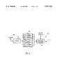
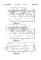
- FIGS. 1, 2, 3, 4, and 5illustrate partial cross-sectional views of an embodiment of a semiconductor component during different stages of manufacture in accordance with the present invention
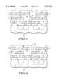
- FIG. 6portrays a partial top view of the semiconductor component of FIG. 5 in accordance with the present invention
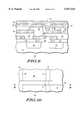
- FIGS. 7, 8, and 9depict partial cross-sectional views of an alternative embodiment of the semiconductor component of FIG. 5 during different stages of manufacture in accordance with the present invention.
- FIG. 10portrays a partial top view of the semiconductor component of FIG. 9 in accordance with the present invention.
- the present inventionallows for the formation of smaller geometry interconnect lines over inter-level vias while maintaining adequate via connection and conductivity.
- the inventionbegins by forming a first conductive layer and patterning the layer to form interconnects (FIG. 1).
- a dielectric layeris then formed on the first conductive layer (FIG. 2).
- a second conductive layeris formed over the dielectric layer (FIG. 2).
- this second conductive layeris formed on the dielectric layer before vias are formed through the dielectric layer to expose the first conductive layer.
- the scribe lines between integrated circuits or other key/alignment mark locations on the waferare cleared by gross lithographic alignment and etch processing which are performed on the second conductive layer.
- This etchis needed to expose alignment marks to allow for the accurate alignment of the subsequently etched vias if inter-metal dielectric chemical mechanical polishing (CMP) is performed.
- CMPinter-metal dielectric chemical mechanical polishing
- alignment marks in the first conductive layerwill show up as indentations in the second conductive layer and these indentations can be used for alignment without the need to clear the scribe lines.
- the second conductive layerwhich is still substantially unpatterned over the integrated circuit (IC) active area, is then etched along with the dielectric layer to form vias not only through the dielectric layer but through the second conductive layer (FIG. 3).
- a third conductive layeris deposited which connects the second conductive layer to the first conductive layer through the vias (FIG. 4).
- the composite of both the second conductive layer and the third conductive layeris now patterned using photolithographic and etch techniques to form interconnects lines 42 (FIG. 5).
- the interconnect width around the via regioncan be reduced to the point of being line-on-line. This allows for smaller logic devices, memory cells, and smaller interconnect buses to be formed on an integrated circuit (IC).
- ICintegrated circuit
- FIGS. 1-10The present invention can be further understood with reference to FIGS. 1-10.
- FIGS. 1, 2, 3, 4, and 5illustrate partial cross-sectional views of an embodiment of a semiconductor component 10 during different stages of manufacture. It is understood that the same reference numerals are used in the figures to denote the same elements.
- Component 10includes a substrate 11 that can be comprised of a semiconductor such as, for example, silicon or gallium arsenide.
- a plurality of semiconductor devices 12 and 13are fabricated in and are supported by substrate 11 using semiconductor processing techniques known to those skilled in the art.
- device 12can represent a field effect transistor area
- device 13can represent a bipolar transistor area. Because devices 12 and 13 can have many different structures, the depicted structures are only for the purpose of illustrating devices 12 and 13.
- a dielectric layer or electrically insulative layer 14is deposited and patterned over substrate 11 and devices 12 and 13 using processes known in the art.
- Layer 14is comprised of electrically insulating materials such as silicon nitride, silicon oxide, tetraethylorthosilicate (TEOS) glass, borophosposilicate glass (BPSG), phosposilicate glass (PSG), spin on glasses (SOG), composite oxides, and/or the like.
- Layer 14has vias exposing contact portions of device 12 and 13.
- An interconnect layer or electrically conductive layer 15is formed over layer 14 and substrate 11.
- Layer 15also overlies and is electrically coupled to devices 12 and 13 through the vias of layer 14.
- Layer 15can be deposited using processes such as, is for example, sputtering, evaporating, deposition, selective growth, or plating techniques.
- Layer 15is comprised of electrically conductive materials such as, for example, aluminum, copper, titanium, tungsten, silicides, or doped polysilicon.
- An etch mask 16is formed over layer 15 and is used to define a pattern for layer 15 during a subsequent etching process. For example, layer 15 can be etched by a fluorine-based dry etchant.
- Mask 16can be comprised of photoresist or any other suitable material that can protect portions of layer 15 from exposure to etchant gas. Mask 16 is removed after the etching process for layer 15.
- a dielectric layer or electrically insulating layer 20is deposited over layers 14 and 15 and substrate 11 using a chemical vapor deposition (CVD), spin-on-glass (SOG), or other similar process.
- Layer 20is preferably planarized using techniques known in the art to provide a substantially planar surface on which to form an additional interconnect layer (e.g. resist etch-back or chemical mechanical polishing (CMP)).
- Layer 20can be similar in composition to layer 14 and can have a thickness of approximately four thousand to ten thousand angstroms.
- An interconnect layer or electrically conductive layer 21is deposited over substrate 11 and layers 20, 15, and 14.
- Layer 21has a surface 22 facing towards layer 20 and an opposite surface 23 facing away from layer 20.
- Layer 21is preferably deposited over layer 20 before a via is etched in layer 20 such that layer 21 is devoid of physical contact with layer 15 and such that layer 21 electrically isolates layers 15 and 21.
- the deposition and composition of layer 21can be similar to that of layer 15.
- Layer 21can have a thickness of approximately four thousand to ten thousand angstroms.
- an etch mask 30is formed over surface 23 of layer 21 and is used to pattern vias 31 and 32 in layer 21. Vias 31 and 32 in layer 21 expose portions of underlying layer 20. Then, mask 30 can also be used to define or extend vias 31 and 32 through layer 20 to expose portions of underlying layer 15. Alternatively, mask 30 can be removed after etching layer 21, and etched layer 21 can be used as an etch mask for layer 20. Accordingly, the via portion of layer 21 extends the via portions of layer 20, and the vias of layer 21 have similar widths as the corresponding vias of layer 20. For best results, mask 30 should not be substantially laterally etched or eroded during the etching of layers 21 or 20.
- the composition of mask 30can be similar to that of mask 16 and is typically photoresist (see mask 16 of FIG. 1).
- the etching of vias 31 and 32produces sidewalls 33 and 34, respectively, in layer 21 and also produces sidewalls 35 and 36, respectively, in layer 20.
- vias 31 and 32can each have a width of approximately eight thousand to fifteen thousand angstroms.
- Vias 31 and 32can be etched using anisotropic etching techniques known in the art.
- an interconnect layer or electrically conductive layer 40is deposited over layer 15 and over surface 23 of layer 21 after the removal of mask 30 from FIG. 3.
- Layer 40is also deposited in vias 31 and 32 of layers 20 and 21.
- Layer 40electrically couples together layers 15 and 21 through vias 31 and 32.
- Layer 40physically contacts and overlies layer 21, and layer 40 physically contacts the portions of layer 15 that are exposed by vias 31 and 32.
- Layer 40should conformally and physically contact sidewalls 33, 34, 35, and 36.
- Layers 21 and 40form a composite interconnect layer 42 for component 10.
- Layer 40is preferably comprised of a refractory anti-reflective material to assist in the subsequent formation of an etch mask over layer 40.
- layer 40can be comprised of barrier materials including, but not limited to, titanium, titanium nitride, or titanium tungsten.
- layer 40is comprised of approximately four hundred to two thousand angstroms of stoichiometric titanium nitride (TiN) because of its anti-reflective properties and because of its ability to be conformally deposited into vias with aspect ratios of greater than approximately two.
- Layer 40can also be comprised of a plurality of layers of refractory materials or a composite refractory metal layer.
- layer 40can be comprised of a two hundred to four hundred angstrom layer of titanium underneath a four hundred to one thousand angstrom layer of titanium nitride.
- Layer 40can be deposited using sputtering techniques, plasma depositions, or other processes known in the art.
- etch mask 41is formed over layer 40.
- Mask 41can be similar to mask 16 (of FIG. 1) and mask 30 (of FIG. 3) and is typically photoresist.
- Mask 41defines an etch pattern for both layers 40 and 21.
- Layers 40 and 21can be sequentially dry etched using techniques and chemistries well known to those skilled in the art. Because mask 41 overlies layer 40 and because layer 40 is comprised of an anti-reflective coating (ARC) material, a separate anti-reflective coating (ARC) is not required as in the prior art. Therefore, the cycle time for manufacturing component 10 is not increased as compared to the increased cycle time and cost incurred by the prior art techniques.
- ARCanti-reflective coating
- component 10is portrayed after the patterning of layers 40 and 21 and after depositing a passivation or dielectric layer 50 over layers 40 and 21.
- Component 10now has a multi-level interconnect system 51 comprised of interconnect layers 15 and 42 and dielectric layers 14, 20, and 50.
- FIG. 6a partial top view of component 10 is portrayed.
- FIG. 5is a cross-sectional illustration of FIG. 6 when FIG. 6 is cut along line 5--5 of FIG. 6. Elements of FIG. 6 that have the same reference numerals as FIG. 5 are the same as the corresponding FIG. 5 elements except that the elements are illustrated in a top perspective view.
- layer 50is removed to facilitate a better explanation of the internal structures of component 10.
- Layers 21 and 40, which form composite layer 42have a smaller line width or pitch compared to the prior art. Layer 42 does not require a larger line width or pitch at a region adjacent to either of vias 31 or 32, as required in the prior art, because of the method of forming layer 42, as explained in more detail hereinafter.
- underlying layer 15(shown as by dashed lines in FIG. 6) has a narrower line width at a portion 65 and has a wider line width at a portion 66 wherein portion 65 is located adjacent to portion 66 and wherein portion 66 is located adjacent to and underlies via 31.
- portion 66has a larger line width to compensate for the potential photolithographic misalignment of via 31 and to prevent layer 40, which is located within via 31, from being inadvertently electrically shorted to a layer which may reside beneath layer 15.
- a portion 68 of layer 15has a larger line width than that of a portion 67 of layer 15.
- interconnect layers that overlie viasalso do not have substantially constant line widths. Instead, when a portion of any prior art interconnect layer is adjacent to or filling an underlying via, that portion around the via is formed having a line width that is larger than other portions of the interconnect layer for alignment tolerance reasons similar to that described for portion 66.
- layer 42has a substantially constant line width.
- Layer 42is not misaligned from either of vias 31 or 32 because vias 31 and 32 are formed after the partial deposition of layer 42.
- layer 21is deposited prior to the formation of vias 31 and 32.
- portions 60, 61, 62, 63, and 64 of layer 42can have substantially or approximately equal widths wherein portions 61 and 63 are located within vias 31 and 32, respectively, wherein portions 62 and 64 are located adjacent to portions 61 and 63, respectively, and wherein portion 60 is located away from both vias 31 and 32 and is located adjacent to portions 62 and 64.
- portion 60is at least approximately two to five microns away from both vias 31 and 32.
- layer 42has a width 69, which is approximately equal to a width of vias 31 and 32.
- the smaller line width of layer 42facilitates a smaller interconnect system 51 and a smaller overall component 10.
- FIGS. 7, 8, and 9depict partial cross-sectional views of a semiconductor component 70 during different stages of manufacture wherein component 70 is an alternative embodiment of component 10 (FIG. 5). Elements of FIGS. 7, 8, and 9 that have the same reference numerals as FIG. 5 are the same as the corresponding FIG. 5 elements.
- Component 70has dielectric or electrically insulating layers 74 and 78 that are similar to layer 20 of FIG. 5.
- Component 70also has interconnect or electrically conductive layers 75 and 79 that are similar to layer 21 of FIG. 5.
- Layer 75is provided over layer 74, and layers 74 and 75 are etched with the same etch mask (not shown) to form an opening, via, or gap 73 between electrically isolated portions 76 and 77 of layer 75 and to define a width for portions 76 and 77 of layer 75. Then, layer 78 is deposited in gap 73 and over layer 75, and layer 79 is provided over layer 78. An etch mask 71 is formed over layer 79 and is used to sequentially pattern layers 79 and 78 to form an opening or via 72. Via 72 is similar in purpose to vias 31 and 32 of FIG. 5 and facilitates the electrical coupling of layer 79 and portion 77 of layer 75.
- via 72is accidentally misaligned relative to underlying portion 77, and therefore, via 72 exposes a portion of gap 73 and layer 15.
- layer 79would be electrically shorted to both layer 15 and portion 77 of layer 75.
- portion 77should be electrically isolated from layer 15.
- a dielectric or electrically insulating layer 80is deposited over layer 79 and is deposited in via 72 and in the exposed portion of gap 73 after the removal of mask 71 (FIG. 7).
- the deposition and composition of layer 80can be similar to that of layer 78.
- Layer 80can have a thickness of approximately five hundred to two thousand angstroms.
- Layer 80physically contacts the sidewalls of via 72 and the exposed portion of gap 73.
- layer 80is adjacent to layers 15, 74, 75, 78, and 79.
- layer 80can be isotropically or anisotropically etched to expose a portion of via 72 and to leave a portion of layer 80 within via 72 and gap 73. Layer 80 remains in via 72 and prevents a subsequently deposited interconnect layer from physically and electrically contacting layer 15 through via 72 and gap 73. Layer 80 has an opening exposing a portion of portion 77 of layer 75.
- An interconnect or electrically conductive layer 90is deposited in via 72 and over layer 79. Layer 90 can be similar in composition and thickness to layer 40 of FIG. 5. Layer 90 is adjacent to and physically contacts portion 77 of layer 75 and layers 79 and 80,. Layer 90 electrically couples layers 79 and portion 77 of layer 75. Layer 90 is not electrically coupled to layer 15 because of the presence of layer 80 in gap 73. Layers 90 and 79 are subsequently patterned using a similar technique as described earlier for layers 40 and 21 in FIG. 4.
- FIG. 10portrays a partial top view of component 70.
- FIG. 9is taken from a section line 9--9 in FIG. 10. Elements of FIG. 10 that have the same reference numerals as FIG. 9 are the same as the corresponding FIG. 9 elements.
- the use of layer 80(FIG. 9) enables the reduction of the line width or pitch of layer 75 near via 72.
- a portion of a prior art interconnect layer that underlies a viahas a wider line width than other portions of the prior art interconnect layer that do not underlie a via in order to prevent the inadvertent shorting of conductive layers underlying the prior art interconnect layer.
- layer 75has a substantially constant line width wherein the region of portion 77 of layer 75 that is adjacent to and that underlies via 72 has the same width as another region of portion 77 of layer 75 that is not next to via 72. As illustrated in FIG. 10, layers 75 and 90 and via 72 have similar widths. Thus, the area required for multi-level interconnect system of component 70 is reduced compared to the prior art.
- the present componentincludes a multi-level interconnect system wherein the interconnect levels have smaller line widths or pitches than the prior art in order to provide a smaller layout for the component.
- a ten to twenty percent reduction in sizehas been accomplished by using the multi-level interconnect system described herein.
- the present componentis also cost effective because it is compatible with existing semiconductor processing techniques and because it does not significantly increase the cycle time for manufacturing the component.
- vias 31 and 32 in FIG. 5can be filled in or plugged after the deposition of layer 40 and before the deposition of layer 50.
- a conventional tungsten plug processcan be used to fill in vias 31 and 32 to improve planarity and improve conductivity in some embodiments.
- the layer 40may be CVD aluminum followed by the TiN or like ARC layer with the CVD aluminum having optional doping concentrations of silicon and/or copper.
- the CVD Al/Tin composite for layer 40may be used to improve via conductivity.
- Tungsten or oxidemay be used to plug opening left in the via or layer 40 itself may be polished to form plug regions within the vias.
Landscapes
- Engineering & Computer Science (AREA)
- Physics & Mathematics (AREA)
- Condensed Matter Physics & Semiconductors (AREA)
- General Physics & Mathematics (AREA)
- Computer Hardware Design (AREA)
- Microelectronics & Electronic Packaging (AREA)
- Power Engineering (AREA)
- Manufacturing & Machinery (AREA)
- Geometry (AREA)
- Internal Circuitry In Semiconductor Integrated Circuit Devices (AREA)
Abstract
Description
Claims (20)
Priority Applications (1)
| Application Number | Priority Date | Filing Date | Title |
|---|---|---|---|
| US09/041,646US5937324A (en) | 1996-08-26 | 1998-03-13 | Method for forming a line-on-line multi-level metal interconnect structure for use in integrated circuits |
Applications Claiming Priority (2)
| Application Number | Priority Date | Filing Date | Title |
|---|---|---|---|
| US08/703,223US5798568A (en) | 1996-08-26 | 1996-08-26 | Semiconductor component with multi-level interconnect system and method of manufacture |
| US09/041,646US5937324A (en) | 1996-08-26 | 1998-03-13 | Method for forming a line-on-line multi-level metal interconnect structure for use in integrated circuits |
Related Parent Applications (1)
| Application Number | Title | Priority Date | Filing Date |
|---|---|---|---|
| US08/703,223DivisionUS5798568A (en) | 1996-08-26 | 1996-08-26 | Semiconductor component with multi-level interconnect system and method of manufacture |
Publications (1)
| Publication Number | Publication Date |
|---|---|
| US5937324Atrue US5937324A (en) | 1999-08-10 |
Family
ID=24824531
Family Applications (2)
| Application Number | Title | Priority Date | Filing Date |
|---|---|---|---|
| US08/703,223Expired - Fee RelatedUS5798568A (en) | 1996-08-26 | 1996-08-26 | Semiconductor component with multi-level interconnect system and method of manufacture |
| US09/041,646Expired - Fee RelatedUS5937324A (en) | 1996-08-26 | 1998-03-13 | Method for forming a line-on-line multi-level metal interconnect structure for use in integrated circuits |
Family Applications Before (1)
| Application Number | Title | Priority Date | Filing Date |
|---|---|---|---|
| US08/703,223Expired - Fee RelatedUS5798568A (en) | 1996-08-26 | 1996-08-26 | Semiconductor component with multi-level interconnect system and method of manufacture |
Country Status (3)
| Country | Link |
|---|---|
| US (2) | US5798568A (en) |
| JP (1) | JPH1092925A (en) |
| KR (1) | KR19980019111A (en) |
Cited By (28)
| Publication number | Priority date | Publication date | Assignee | Title |
|---|---|---|---|---|
| US6159842A (en)* | 1999-01-11 | 2000-12-12 | Taiwan Semiconductor Manufacturing Company | Method for fabricating a hybrid low-dielectric-constant intermetal dielectric (IMD) layer with improved reliability for multilevel interconnections |
| US6277747B1 (en)* | 1998-11-09 | 2001-08-21 | Sony Corporation | Method for removal of etch residue immediately after etching a SOG layer |
| US6303999B1 (en)* | 1997-12-12 | 2001-10-16 | Samsung Electronics Co., Ltd. | Interconnect structure with a passivation layer and chip pad |
| US6335567B1 (en)* | 1998-10-07 | 2002-01-01 | Samsung Electronics Co., Ltd. | Semiconductor device having stress reducing laminate and method for manufacturing the same |
| US6455436B1 (en)* | 1999-01-08 | 2002-09-24 | Matsushita Electric Industrial Co., Ltd. | Method of fabricating semiconductor device |
| US6459154B2 (en)* | 2000-06-23 | 2002-10-01 | Samsung Electronics Co., Ltd. | Bonding pad structure of a semiconductor device and method of fabricating the same |
| US20040251549A1 (en)* | 2003-06-11 | 2004-12-16 | Tai-Chun Huang | Hybrid copper/low k dielectric interconnect integration method and device |
| US20050098896A1 (en)* | 2003-11-12 | 2005-05-12 | Tai-Chun Huang | Integration film scheme for copper / low-k interconnect |
| US7247523B1 (en) | 2002-11-08 | 2007-07-24 | Amkor Technology, Inc. | Two-sided wafer escape package |
| US7361533B1 (en) | 2002-11-08 | 2008-04-22 | Amkor Technology, Inc. | Stacked embedded leadframe |
| US7572681B1 (en) | 2005-12-08 | 2009-08-11 | Amkor Technology, Inc. | Embedded electronic component package |
| US7723210B2 (en) | 2002-11-08 | 2010-05-25 | Amkor Technology, Inc. | Direct-write wafer level chip scale package |
| US7902660B1 (en) | 2006-05-24 | 2011-03-08 | Amkor Technology, Inc. | Substrate for semiconductor device and manufacturing method thereof |
| US20110171827A1 (en)* | 2010-01-14 | 2011-07-14 | International Business Machines Corporation | Three Dimensional Integration and Methods of Through Silicon Via Creation |
| US20110171582A1 (en)* | 2010-01-14 | 2011-07-14 | International Business Machines Corporation | Three Dimensional Integration With Through Silicon Vias Having Multiple Diameters |
| US8294276B1 (en) | 2010-05-27 | 2012-10-23 | Amkor Technology, Inc. | Semiconductor device and fabricating method thereof |
| US8324511B1 (en) | 2010-04-06 | 2012-12-04 | Amkor Technology, Inc. | Through via nub reveal method and structure |
| US8390130B1 (en) | 2011-01-06 | 2013-03-05 | Amkor Technology, Inc. | Through via recessed reveal structure and method |
| US8440554B1 (en) | 2010-08-02 | 2013-05-14 | Amkor Technology, Inc. | Through via connected backside embedded circuit features structure and method |
| US8487445B1 (en) | 2010-10-05 | 2013-07-16 | Amkor Technology, Inc. | Semiconductor device having through electrodes protruding from dielectric layer |
| US8552548B1 (en) | 2011-11-29 | 2013-10-08 | Amkor Technology, Inc. | Conductive pad on protruding through electrode semiconductor device |
| US8791501B1 (en) | 2010-12-03 | 2014-07-29 | Amkor Technology, Inc. | Integrated passive device structure and method |
| US8796561B1 (en) | 2009-10-05 | 2014-08-05 | Amkor Technology, Inc. | Fan out build up substrate stackable package and method |
| US8937381B1 (en) | 2009-12-03 | 2015-01-20 | Amkor Technology, Inc. | Thin stackable package and method |
| US9048298B1 (en) | 2012-03-29 | 2015-06-02 | Amkor Technology, Inc. | Backside warpage control structure and fabrication method |
| US9129943B1 (en) | 2012-03-29 | 2015-09-08 | Amkor Technology, Inc. | Embedded component package and fabrication method |
| US9691734B1 (en) | 2009-12-07 | 2017-06-27 | Amkor Technology, Inc. | Method of forming a plurality of electronic component packages |
| US20220199522A1 (en)* | 2020-12-17 | 2022-06-23 | Samsung Electronics Co., Ltd. | Semiconductor device and method of fabricating the same |
Families Citing this family (14)
| Publication number | Priority date | Publication date | Assignee | Title |
|---|---|---|---|---|
| KR100272859B1 (en)* | 1997-06-28 | 2000-12-01 | 김영환 | Manufacturing method of metal interconnection layer in semiconductor device |
| JPH11233632A (en)* | 1997-11-26 | 1999-08-27 | Texas Instr Inc <Ti> | Integrated circuit conductor interconnecting method |
| US6239491B1 (en)* | 1998-05-18 | 2001-05-29 | Lsi Logic Corporation | Integrated circuit structure with thin dielectric between at least local interconnect level and first metal interconnect level, and process for making same |
| JP3169907B2 (en)* | 1998-09-25 | 2001-05-28 | 日本電気株式会社 | Multilayer wiring structure and method of manufacturing the same |
| US6965165B2 (en) | 1998-12-21 | 2005-11-15 | Mou-Shiung Lin | Top layers of metal for high performance IC's |
| US6936531B2 (en) | 1998-12-21 | 2005-08-30 | Megic Corporation | Process of fabricating a chip structure |
| TW439303B (en)* | 1999-11-22 | 2001-06-07 | Nat Science Council | Manufacturing method of field emission device |
| AT4149U1 (en)* | 1999-12-03 | 2001-02-26 | Austria Mikrosysteme Int | METHOD FOR PRODUCING STRUCTURES IN CHIPS |
| US6498088B1 (en)* | 2000-11-09 | 2002-12-24 | Micron Technology, Inc. | Stacked local interconnect structure and method of fabricating same |
| US7932603B2 (en) | 2001-12-13 | 2011-04-26 | Megica Corporation | Chip structure and process for forming the same |
| US7576013B2 (en)* | 2004-07-27 | 2009-08-18 | United Microelectronics Corp. | Method of relieving wafer stress |
| US7875546B1 (en)* | 2006-09-01 | 2011-01-25 | National Semiconductor Corporation | System and method for preventing metal corrosion on bond pads |
| US7557455B1 (en) | 2007-02-27 | 2009-07-07 | National Semiconductor Corporation | System and apparatus that reduce corrosion of an integrated circuit through its bond pads |
| US8282846B2 (en)* | 2010-02-27 | 2012-10-09 | National Semiconductor Corporation | Metal interconnect structure with a side wall spacer that protects an ARC layer and a bond pad from corrosion and method of forming the metal interconnect structure |
Citations (8)
| Publication number | Priority date | Publication date | Assignee | Title |
|---|---|---|---|---|
| US4541893A (en)* | 1984-05-15 | 1985-09-17 | Advanced Micro Devices, Inc. | Process for fabricating pedestal interconnections between conductive layers in an integrated circuit |
| US4656732A (en)* | 1984-09-26 | 1987-04-14 | Texas Instruments Incorporated | Integrated circuit fabrication process |
| US4977105A (en)* | 1988-03-15 | 1990-12-11 | Mitsubishi Denki Kabushiki Kaisha | Method for manufacturing interconnection structure in semiconductor device |
| US5243221A (en)* | 1989-10-25 | 1993-09-07 | At&T Bell Laboratories | Aluminum metallization doped with iron and copper to prevent electromigration |
| US5281850A (en)* | 1991-08-07 | 1994-01-25 | Oki Electric Industry Co., Ltd. | Semiconductor device multilayer metal layer structure including conductive migration resistant layers |
| US5294837A (en)* | 1990-09-28 | 1994-03-15 | Kabushiki Kaisha Toshiba | Semiconductor integrated circuit capable of correcting wiring skew |
| US5374592A (en)* | 1992-09-22 | 1994-12-20 | Sgs-Thomson Microelectronics, Inc. | Method for forming an aluminum metal contact |
| US5510294A (en)* | 1991-12-31 | 1996-04-23 | Sgs-Thomson Microelectronics, Inc. | Method of forming vias for multilevel metallization |
- 1996
- 1996-08-26USUS08/703,223patent/US5798568A/ennot_activeExpired - Fee Related
- 1997
- 1997-08-22JPJP9242197Apatent/JPH1092925A/enactivePending
- 1997-08-26KRKR1019970042074Apatent/KR19980019111A/ennot_activeWithdrawn
- 1998
- 1998-03-13USUS09/041,646patent/US5937324A/ennot_activeExpired - Fee Related
Patent Citations (8)
| Publication number | Priority date | Publication date | Assignee | Title |
|---|---|---|---|---|
| US4541893A (en)* | 1984-05-15 | 1985-09-17 | Advanced Micro Devices, Inc. | Process for fabricating pedestal interconnections between conductive layers in an integrated circuit |
| US4656732A (en)* | 1984-09-26 | 1987-04-14 | Texas Instruments Incorporated | Integrated circuit fabrication process |
| US4977105A (en)* | 1988-03-15 | 1990-12-11 | Mitsubishi Denki Kabushiki Kaisha | Method for manufacturing interconnection structure in semiconductor device |
| US5243221A (en)* | 1989-10-25 | 1993-09-07 | At&T Bell Laboratories | Aluminum metallization doped with iron and copper to prevent electromigration |
| US5294837A (en)* | 1990-09-28 | 1994-03-15 | Kabushiki Kaisha Toshiba | Semiconductor integrated circuit capable of correcting wiring skew |
| US5281850A (en)* | 1991-08-07 | 1994-01-25 | Oki Electric Industry Co., Ltd. | Semiconductor device multilayer metal layer structure including conductive migration resistant layers |
| US5510294A (en)* | 1991-12-31 | 1996-04-23 | Sgs-Thomson Microelectronics, Inc. | Method of forming vias for multilevel metallization |
| US5374592A (en)* | 1992-09-22 | 1994-12-20 | Sgs-Thomson Microelectronics, Inc. | Method for forming an aluminum metal contact |
Cited By (67)
| Publication number | Priority date | Publication date | Assignee | Title |
|---|---|---|---|---|
| US6303999B1 (en)* | 1997-12-12 | 2001-10-16 | Samsung Electronics Co., Ltd. | Interconnect structure with a passivation layer and chip pad |
| US6596633B2 (en) | 1997-12-12 | 2003-07-22 | Samsung Electronics Co., Ltd. | Method for manufacturing a semiconductor device |
| US6335567B1 (en)* | 1998-10-07 | 2002-01-01 | Samsung Electronics Co., Ltd. | Semiconductor device having stress reducing laminate and method for manufacturing the same |
| US6555462B2 (en) | 1998-10-07 | 2003-04-29 | Samsung Electronics Co., Ltd. | Semiconductor device having stress reducing laminate and method for manufacturing the same |
| US6277747B1 (en)* | 1998-11-09 | 2001-08-21 | Sony Corporation | Method for removal of etch residue immediately after etching a SOG layer |
| US6455436B1 (en)* | 1999-01-08 | 2002-09-24 | Matsushita Electric Industrial Co., Ltd. | Method of fabricating semiconductor device |
| US6780779B2 (en)* | 1999-01-08 | 2004-08-24 | Matsushita Electric Industrial Co., Ltd. | Method of fabricating semiconductor device |
| US6159842A (en)* | 1999-01-11 | 2000-12-12 | Taiwan Semiconductor Manufacturing Company | Method for fabricating a hybrid low-dielectric-constant intermetal dielectric (IMD) layer with improved reliability for multilevel interconnections |
| US6459154B2 (en)* | 2000-06-23 | 2002-10-01 | Samsung Electronics Co., Ltd. | Bonding pad structure of a semiconductor device and method of fabricating the same |
| US8298866B1 (en) | 2002-11-08 | 2012-10-30 | Amkor Technology, Inc. | Wafer level package and fabrication method |
| US8119455B1 (en) | 2002-11-08 | 2012-02-21 | Amkor Technology, Inc. | Wafer level package fabrication method |
| US8710649B1 (en) | 2002-11-08 | 2014-04-29 | Amkor Technology, Inc. | Wafer level package and fabrication method |
| US7247523B1 (en) | 2002-11-08 | 2007-07-24 | Amkor Technology, Inc. | Two-sided wafer escape package |
| US7361533B1 (en) | 2002-11-08 | 2008-04-22 | Amkor Technology, Inc. | Stacked embedded leadframe |
| US7420272B1 (en) | 2002-11-08 | 2008-09-02 | Amkor Technology, Inc. | Two-sided wafer escape package |
| US8501543B1 (en) | 2002-11-08 | 2013-08-06 | Amkor Technology, Inc. | Direct-write wafer level chip scale package |
| US7692286B1 (en) | 2002-11-08 | 2010-04-06 | Amkor Technology, Inc. | Two-sided fan-out wafer escape package |
| US7714431B1 (en) | 2002-11-08 | 2010-05-11 | Amkor Technology, Inc. | Electronic component package comprising fan-out and fan-in traces |
| US7723210B2 (en) | 2002-11-08 | 2010-05-25 | Amkor Technology, Inc. | Direct-write wafer level chip scale package |
| US8486764B1 (en) | 2002-11-08 | 2013-07-16 | Amkor Technology, Inc. | Wafer level package and fabrication method |
| US7932595B1 (en) | 2002-11-08 | 2011-04-26 | Amkor Technology, Inc. | Electronic component package comprising fan-out traces |
| US8952522B1 (en) | 2002-11-08 | 2015-02-10 | Amkor Technology, Inc. | Wafer level package and fabrication method |
| US10665567B1 (en) | 2002-11-08 | 2020-05-26 | Amkor Technology, Inc. | Wafer level package and fabrication method |
| US9054117B1 (en) | 2002-11-08 | 2015-06-09 | Amkor Technology, Inc. | Wafer level package and fabrication method |
| US9406645B1 (en) | 2002-11-08 | 2016-08-02 | Amkor Technology, Inc. | Wafer level package and fabrication method |
| US8188584B1 (en) | 2002-11-08 | 2012-05-29 | Amkor Technology, Inc. | Direct-write wafer level chip scale package |
| US9871015B1 (en) | 2002-11-08 | 2018-01-16 | Amkor Technology, Inc. | Wafer level package and fabrication method |
| US8691632B1 (en) | 2002-11-08 | 2014-04-08 | Amkor Technology, Inc. | Wafer level package and fabrication method |
| US20040251549A1 (en)* | 2003-06-11 | 2004-12-16 | Tai-Chun Huang | Hybrid copper/low k dielectric interconnect integration method and device |
| US20050098896A1 (en)* | 2003-11-12 | 2005-05-12 | Tai-Chun Huang | Integration film scheme for copper / low-k interconnect |
| US7244673B2 (en) | 2003-11-12 | 2007-07-17 | Taiwan Semiconductor Manufacturing Company, Ltd. | Integration film scheme for copper / low-k interconnect |
| US7977163B1 (en) | 2005-12-08 | 2011-07-12 | Amkor Technology, Inc. | Embedded electronic component package fabrication method |
| US7572681B1 (en) | 2005-12-08 | 2009-08-11 | Amkor Technology, Inc. | Embedded electronic component package |
| US7902660B1 (en) | 2006-05-24 | 2011-03-08 | Amkor Technology, Inc. | Substrate for semiconductor device and manufacturing method thereof |
| US8796561B1 (en) | 2009-10-05 | 2014-08-05 | Amkor Technology, Inc. | Fan out build up substrate stackable package and method |
| US8937381B1 (en) | 2009-12-03 | 2015-01-20 | Amkor Technology, Inc. | Thin stackable package and method |
| US9691734B1 (en) | 2009-12-07 | 2017-06-27 | Amkor Technology, Inc. | Method of forming a plurality of electronic component packages |
| US10546833B2 (en) | 2009-12-07 | 2020-01-28 | Amkor Technology, Inc. | Method of forming a plurality of electronic component packages |
| US8415238B2 (en) | 2010-01-14 | 2013-04-09 | International Business Machines Corporation | Three dimensional integration and methods of through silicon via creation |
| US8399180B2 (en) | 2010-01-14 | 2013-03-19 | International Business Machines Corporation | Three dimensional integration with through silicon vias having multiple diameters |
| US8569154B2 (en) | 2010-01-14 | 2013-10-29 | International Business Machines Corporation | Three dimensional integration and methods of through silicon via creation |
| US20110171827A1 (en)* | 2010-01-14 | 2011-07-14 | International Business Machines Corporation | Three Dimensional Integration and Methods of Through Silicon Via Creation |
| US20110171582A1 (en)* | 2010-01-14 | 2011-07-14 | International Business Machines Corporation | Three Dimensional Integration With Through Silicon Vias Having Multiple Diameters |
| US8492252B2 (en) | 2010-01-14 | 2013-07-23 | International Business Machines Corporation | Three dimensional integration and methods of through silicon via creation |
| US8586431B2 (en) | 2010-01-14 | 2013-11-19 | International Business Machines Corporation | Three dimensional integration and methods of through silicon via creation |
| US8324511B1 (en) | 2010-04-06 | 2012-12-04 | Amkor Technology, Inc. | Through via nub reveal method and structure |
| US9324614B1 (en) | 2010-04-06 | 2016-04-26 | Amkor Technology, Inc. | Through via nub reveal method and structure |
| US8294276B1 (en) | 2010-05-27 | 2012-10-23 | Amkor Technology, Inc. | Semiconductor device and fabricating method thereof |
| US8440554B1 (en) | 2010-08-02 | 2013-05-14 | Amkor Technology, Inc. | Through via connected backside embedded circuit features structure and method |
| US9159672B1 (en) | 2010-08-02 | 2015-10-13 | Amkor Technology, Inc. | Through via connected backside embedded circuit features structure and method |
| US8900995B1 (en) | 2010-10-05 | 2014-12-02 | Amkor Technology, Inc. | Semiconductor device and manufacturing method thereof |
| US8487445B1 (en) | 2010-10-05 | 2013-07-16 | Amkor Technology, Inc. | Semiconductor device having through electrodes protruding from dielectric layer |
| US8791501B1 (en) | 2010-12-03 | 2014-07-29 | Amkor Technology, Inc. | Integrated passive device structure and method |
| US8390130B1 (en) | 2011-01-06 | 2013-03-05 | Amkor Technology, Inc. | Through via recessed reveal structure and method |
| US9082833B1 (en) | 2011-01-06 | 2015-07-14 | Amkor Technology, Inc. | Through via recessed reveal structure and method |
| US8552548B1 (en) | 2011-11-29 | 2013-10-08 | Amkor Technology, Inc. | Conductive pad on protruding through electrode semiconductor device |
| US9431323B1 (en) | 2011-11-29 | 2016-08-30 | Amkor Technology, Inc. | Conductive pad on protruding through electrode |
| US8981572B1 (en) | 2011-11-29 | 2015-03-17 | Amkor Technology, Inc. | Conductive pad on protruding through electrode semiconductor device |
| US9947623B1 (en) | 2011-11-29 | 2018-04-17 | Amkor Technology, Inc. | Semiconductor device comprising a conductive pad on a protruding-through electrode |
| US11043458B2 (en) | 2011-11-29 | 2021-06-22 | Amkor Technology Singapore Holding Pte. Ltd. | Method of manufacturing an electronic device comprising a conductive pad on a protruding-through electrode |
| US10410967B1 (en) | 2011-11-29 | 2019-09-10 | Amkor Technology, Inc. | Electronic device comprising a conductive pad on a protruding-through electrode |
| US9129943B1 (en) | 2012-03-29 | 2015-09-08 | Amkor Technology, Inc. | Embedded component package and fabrication method |
| US9048298B1 (en) | 2012-03-29 | 2015-06-02 | Amkor Technology, Inc. | Backside warpage control structure and fabrication method |
| US10014240B1 (en) | 2012-03-29 | 2018-07-03 | Amkor Technology, Inc. | Embedded component package and fabrication method |
| US20220199522A1 (en)* | 2020-12-17 | 2022-06-23 | Samsung Electronics Co., Ltd. | Semiconductor device and method of fabricating the same |
| US11664310B2 (en)* | 2020-12-17 | 2023-05-30 | Samsung Electronics Co., Ltd. | Semiconductor device and method of fabricating the same |
| US12218046B2 (en) | 2020-12-17 | 2025-02-04 | Samsung Electronics Co., Ltd. | Semiconductor device and method of fabricating the same |
Also Published As
| Publication number | Publication date |
|---|---|
| JPH1092925A (en) | 1998-04-10 |
| US5798568A (en) | 1998-08-25 |
| KR19980019111A (en) | 1998-06-05 |
Similar Documents
| Publication | Publication Date | Title |
|---|---|---|
| US5937324A (en) | Method for forming a line-on-line multi-level metal interconnect structure for use in integrated circuits | |
| US6090700A (en) | Metallization method for forming interconnects in an integrated circuit | |
| US6140238A (en) | Self-aligned copper interconnect structure and method of manufacturing same | |
| US8461692B2 (en) | Semiconductor device structures including damascene trenches with conductive structures and related method | |
| EP0176010B1 (en) | Integrated circuit fabrication process and device | |
| US6281585B1 (en) | Air gap dielectric in self-aligned via structures | |
| US5702982A (en) | Method for making metal contacts and interconnections concurrently on semiconductor integrated circuits | |
| US5087591A (en) | Contact etch process | |
| US8072074B2 (en) | Semiconductor device and method of manufacturing same | |
| US5977599A (en) | Formation of a metal via using a raised metal plug structure | |
| EP0534631B1 (en) | Method of forming vias structure obtained | |
| US6576550B1 (en) | ‘Via first’ dual damascene process for copper metallization | |
| US5109267A (en) | Method for producing an integrated circuit structure with a dense multilayer metallization pattern | |
| US6348734B1 (en) | Self-aligned copper interconnect architecture with enhanced copper diffusion barrier | |
| US7050290B2 (en) | Integrated capacitor | |
| US7112504B2 (en) | Method of forming metal-insulator-metal (MIM) capacitors at copper process | |
| US6472308B1 (en) | Borderless vias on bottom metal | |
| US6054389A (en) | Method of forming metal conducting pillars | |
| US6232215B1 (en) | Method for forming increased density for interconnection metallization | |
| US6339027B1 (en) | Process for borderless stop in tin via formation | |
| CN111211095B (en) | Method for manufacturing conductive interconnection line | |
| US7112537B2 (en) | Method of fabricating interconnection structure of semiconductor device | |
| JPH09129730A (en) | Method for manufacturing semiconductor device | |
| KR0165379B1 (en) | Layer wiring method of semiconductor device | |
| KR100313604B1 (en) | Method of planarizing an insulating layer in semiconductor devices |
Legal Events
| Date | Code | Title | Description |
|---|---|---|---|
| FPAY | Fee payment | Year of fee payment:4 | |
| AS | Assignment | Owner name:FREESCALE SEMICONDUCTOR, INC., TEXAS Free format text:ASSIGNMENT OF ASSIGNORS INTEREST;ASSIGNOR:MOTOROLA, INC.;REEL/FRAME:015698/0657 Effective date:20040404 Owner name:FREESCALE SEMICONDUCTOR, INC.,TEXAS Free format text:ASSIGNMENT OF ASSIGNORS INTEREST;ASSIGNOR:MOTOROLA, INC.;REEL/FRAME:015698/0657 Effective date:20040404 | |
| FPAY | Fee payment | Year of fee payment:8 | |
| AS | Assignment | Owner name:CITIBANK, N.A. AS COLLATERAL AGENT, NEW YORK Free format text:SECURITY AGREEMENT;ASSIGNORS:FREESCALE SEMICONDUCTOR, INC.;FREESCALE ACQUISITION CORPORATION;FREESCALE ACQUISITION HOLDINGS CORP.;AND OTHERS;REEL/FRAME:018855/0129 Effective date:20061201 Owner name:CITIBANK, N.A. AS COLLATERAL AGENT,NEW YORK Free format text:SECURITY AGREEMENT;ASSIGNORS:FREESCALE SEMICONDUCTOR, INC.;FREESCALE ACQUISITION CORPORATION;FREESCALE ACQUISITION HOLDINGS CORP.;AND OTHERS;REEL/FRAME:018855/0129 Effective date:20061201 | |
| AS | Assignment | Owner name:CITIBANK, N.A., AS COLLATERAL AGENT,NEW YORK Free format text:SECURITY AGREEMENT;ASSIGNOR:FREESCALE SEMICONDUCTOR, INC.;REEL/FRAME:024397/0001 Effective date:20100413 Owner name:CITIBANK, N.A., AS COLLATERAL AGENT, NEW YORK Free format text:SECURITY AGREEMENT;ASSIGNOR:FREESCALE SEMICONDUCTOR, INC.;REEL/FRAME:024397/0001 Effective date:20100413 | |
| REMI | Maintenance fee reminder mailed | ||
| LAPS | Lapse for failure to pay maintenance fees | ||
| STCH | Information on status: patent discontinuation | Free format text:PATENT EXPIRED DUE TO NONPAYMENT OF MAINTENANCE FEES UNDER 37 CFR 1.362 | |
| FP | Lapsed due to failure to pay maintenance fee | Effective date:20110810 | |
| AS | Assignment | Owner name:FREESCALE SEMICONDUCTOR, INC., TEXAS Free format text:PATENT RELEASE;ASSIGNOR:CITIBANK, N.A., AS COLLATERAL AGENT;REEL/FRAME:037356/0143 Effective date:20151207 Owner name:FREESCALE SEMICONDUCTOR, INC., TEXAS Free format text:PATENT RELEASE;ASSIGNOR:CITIBANK, N.A., AS COLLATERAL AGENT;REEL/FRAME:037356/0553 Effective date:20151207 Owner name:FREESCALE SEMICONDUCTOR, INC., TEXAS Free format text:PATENT RELEASE;ASSIGNOR:CITIBANK, N.A., AS COLLATERAL AGENT;REEL/FRAME:037354/0225 Effective date:20151207 |