US5936757A - Thin film actuated mirror array - Google Patents
Thin film actuated mirror arrayDownload PDFInfo
- Publication number
- US5936757A US5936757AUS08/877,645US87764597AUS5936757AUS 5936757 AUS5936757 AUS 5936757AUS 87764597 AUS87764597 AUS 87764597AUS 5936757 AUS5936757 AUS 5936757A
- Authority
- US
- United States
- Prior art keywords
- actuating structure
- actuated mirror
- motion
- mirror
- thin film
- Prior art date
- Legal status (The legal status is an assumption and is not a legal conclusion. Google has not performed a legal analysis and makes no representation as to the accuracy of the status listed.)
- Expired - Lifetime
Links
Images


Classifications
- G—PHYSICS
- G02—OPTICS
- G02B—OPTICAL ELEMENTS, SYSTEMS OR APPARATUS
- G02B26/00—Optical devices or arrangements for the control of light using movable or deformable optical elements
- G02B26/08—Optical devices or arrangements for the control of light using movable or deformable optical elements for controlling the direction of light
- G02B26/0816—Optical devices or arrangements for the control of light using movable or deformable optical elements for controlling the direction of light by means of one or more reflecting elements
- G02B26/0833—Optical devices or arrangements for the control of light using movable or deformable optical elements for controlling the direction of light by means of one or more reflecting elements the reflecting element being a micromechanical device, e.g. a MEMS mirror, DMD
- G02B26/0858—Optical devices or arrangements for the control of light using movable or deformable optical elements for controlling the direction of light by means of one or more reflecting elements the reflecting element being a micromechanical device, e.g. a MEMS mirror, DMD the reflecting means being moved or deformed by piezoelectric means
Definitions
- the present inventionrelates to an optical projection system; and, more particularly, to an array of M ⁇ N thin film actuated mirrors for use in the system.
- an optical projection systemis known to be capable of providing a high quality display in a large scale.
- light from a lampis uniformly illuminated onto an array of, e.g., M ⁇ N, actuated mirrors such that each of the mirrors is coupled with each of the actuators.
- the actuatorsmay be made of an electrodisplacive material such as a piezoelectric or an electrostrictive material which deforms in response to an electric field applied thereto.
- the reflected light beam from each of the mirrorsis incident upon an aperture of a baffle.
- an electrical signal to each of the actuatorsBy applying an electrical signal to each of the actuators, the relative position of each of the mirrors to the incident light beam is altered, thereby causing a deviation in the optical path of the reflected beam from each of the mirrors.
- the optical path of each of the reflected beamsis varied, the amount of light reflected from each of the mirrors which passes through the aperture is changed, thereby modulating the intensity of the beam.
- the modulated beams through the apertureare transmitted onto a projection screen via an appropriate optical device such as a projection lens, to thereby display an image thereon.
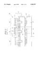
- FIG. 1there is shown a cross sectional view of an M ⁇ N electrodisplacive actuated mirror array 10 for use in an optical projection system, disclosed in a commonly owned application, U.S. Ser. No. 08/278,472, entitled “ELECTRODISPLACIVE ACTUATED MIRROR ARRAY" now U.S. Pat. No.
- 5,735,026,comprising: an active matrix 11 including a substrate 12 and an array of M ⁇ N transistors thereon; an array 13 of M ⁇ N electrodisplacive actuators 30, each of the electrodisplacive actuators 30 including a pair of actuating members 14, 15, a pair of bias electrodes 16, 17, and a common signal electrode 18; an array 19 of M ⁇ N hinges 31, each of the hinges 31 fitted in each of the electrodisplacive actuators 30; an array 20 of M ⁇ N connecting terminals 22, each of the connecting terminals 22 being used for electrically connecting each of the signal electrodes 18 with the active matrix 11; and an array 21 of M ⁇ N mirrors 23, each of the mirrors 23 being mounted on top of each of the M ⁇ N hinges 31.
- a primary object of the present inventionis to provide a method for manufacturing an array of M ⁇ N actuated mirrors, which dispenses with the use of a thin electrodiplacive ceramic wafer.
- an array of M ⁇ N thin film actuated mirrorsfor use in an optical projection system, the array comprising: an active matrix including a substrate, an array of M ⁇ N transistors and an array of M ⁇ N connecting terminals; an array of M ⁇ N thin film actuating structures, each of the actuating structures being provided with a top and a bottom surfaces, a proximal and a distal ends, each of the actuating structures including at least a thin film layer of a motion-inducing material having a top and bottom surfaces, and a first and a second electrodes of a specific thickness, the first electrode being placed on the top surface of the motion-inducing layer and the second electrode, on the bottom surface thereof, wherein an electrical signal applied across the motion-inducing layer between the first and second electrodes causes a deformation of the motion-inducing layer, and hence the actuating structure; an array of M ⁇ N supporting members, each of the supporting members being provided with a top and a bottom
- a novel method for manufacturing an array of M ⁇ N actuated mirrors for use in an optical projection systemcomprising the steps of: (a) providing an active matrix having a top and a bottom surfaces, the active matrix including a substrate, an array of M ⁇ N transistors and an array of M ⁇ N connecting terminals; (b) forming a supporting layer on the top surface of the active matrix, the supporting layer having an array of M ⁇ N pedestals corresponding to the array of M ⁇ N supporting members in the array of M ⁇ N thin film actuated mirrors and a sacrificial area; (c) treating the sacrificial area of the supporting layer to be removable; (d) depositing a first thin film electrode layer on the supporting layer; (e)providing a thin film motion-inducing layer on the first thin film electrode layer; (f) forming a second thin film electrode layer on the thin film motion-inducing layer; (g) depositing a mirror
- FIG. 1shows a cross sectional view of an array of M ⁇ N electrodisplacive actuated mirrors previously disclosed
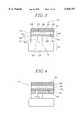
- FIG. 2represents a cross sectional view of an array of M ⁇ N thin film actuated mirrors is accordance with a preferred embodiment of the present invention
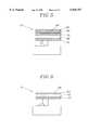
- FIG. 3illustrates a detailed cross sectional view of an thin film actuated mirror of the first embodiment shown in FIG. 2;
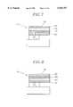
- FIG. 4offers a cross sectional view of an actuated mirror of the first embodiment with an elastic layer added intermediate the mirror and the first electrode;
- FIG. 5depicts a cross sectional view of an actuated mirror of the first embodiment with an elastic layer placed on bottom of the second electrode;
- FIG. 6presents a cross sectional view of an actuated mirror of the first embodiment having the first electrode made of a light reflecting material and provided with the first and second electrodes having a different thickness;
- FIG. 7describes a cross sectional view of an actuated mirror of the first embodiment having the first electrode made of a light reflecting material and provided with an elastic layer placed on the bottom surface of the actuating structure;
- FIG. 8explains a cross sectional view of an actuated mirror of the first embodiment with an elastic layer placed on top of the first electrode and made of a light reflecting material;
- FIGS. 9A and 9Bdemonstrate a cross sectional view of an actuated mirror of the first embodiment having either one of the top and bottom surfaces of the motion-inducing layer in each of the actuating structure covered partially with the first and second electrodes;
- FIG. 10discloses a cross sectional view of an actuated mirror of the first embodiment in an actuated state
- FIG. 11provides a cross sectional view of an actuated mirror of the second embodiment having a bimorph structure
- FIG. 12displays a cross sectional view of an actuated mirror of the second embodiment having the first electrode made of a light reflecting material
- FIGS. 13A to 13Freproduce schematic cross sectional views setting forth the manufacturing steps for the first embodiment in accordance with the present invention.
- FIGS. 2 to 13there are provided schematic cross sectional views of the inventive array of M ⁇ N thin film actuated mirrors for use in an optical projection system, wherein M and N are integers, in accordance with preferred embodiments of the present invention. It should be noted that like parts appearing in FIGS. 2 to 13 are represented by like reference numerals.
- FIG. 2there is illustrated a cross sectional view of a first embodiment of an array 50 of M ⁇ N thin film actuated mirrors 51, comprising an active matrix 52, an array 53 of M ⁇ N thin film actuating structures 54, an array 55 of M ⁇ N supporting members 56 and an array 57 of M ⁇ N mirrors 58.
- FIG. 3represents a detailed cross sectional view of a thin film actuated mirror 51 shown in FIG. 2.
- the active matrix 52includes a substrate 59, an array of M ⁇ N transistors (not shown) and an array 60 of M ⁇ N connecting terminals 61.
- Each of the thin film actuating structures 54is provided with a top and a bottom surfaces 61, 63, a proximal and a distal ends, 64, 65, and further includes at least a thin film layer 66 of a motion inducing material having a top and a bottom surfaces 67, 68 and a first and second electrodes 69, 70 of a specific thickness, made of, e.g., a metal such as gold (Au) or silver (Ag), the first electrode 69 having a top surface 39.
- a metalsuch as gold (Au) or silver (Ag
- the first electrode 69is placed on the top surface 67 of the motion-inducing thin film layer 66 and the second electrode 70, on the bottom surface 68 thereof.
- the motion-inducing thin film layer 66is made of a piezoelectric ceramic, an electrostrictive ceramic, a magnetrostrictive ceramic or a piezoelectric polymer. In the case when the motion-inducing thin film layer is made of a piezoelectric ceramic or a piezoelectric polymer, it must be poled.
- Each of the M ⁇ N supporting members 56is used for holding each of the actuating structures 54 in place and also for electrically connecting the second electrode 70 in each of the actuating structures 54 with the corresponding connecting terminals 61 on the active matrix 52 by being provided with a conduit 73 made of an electrically conductive material, e.g., a metal.
- each of the actuating structures 54is cantilevered from each of the supporting members 56 by being mounted on the top surface 71 of each of the supporting members 56 at the bottom surface 63 of each of the actuating structures 54 at the proximal end 64 thereof, and the bottom surface 72 of each of the supporting members 56 is placed on top of the active matrix 52.
- Each of the M ⁇ N mirrors 58 for reflecting light beamsis placed on top of each of the actuating structures 54.
- the combined thickness of the mirror 58 and the first electrode 69 in each of the thin film actuated mirrors 51must be different from that of the second electrode therein for the deformation thereof to take place. If not, an elastic layer 88 having a top surface 40 must be further provided to each of the actuated mirrors 51.
- the elastic layer 88can be placed either intermediate the mirror 58 and the first electrode 69 or on bottom of the second electrode 70 in each of the actuated mirrors 51, as illustrated in FIGS. 4 and 5.
- the electrically conducting material making up the first electrode 69can be also light reflecting, e.g., aluminum (Al), which will allow the top surface 39 of the first electrode function also as the mirror 58 in each of the thin film actuated mirrors 51.
- the first and the second electrodes 69, 70in order for each of the thin film actuated mirrors 51 to function properly, must be of a different thickness or each of the thin film actuated mirrors 51 must be provided with an elastic layer 88 placed on the bottom surface of each of the actuating structures therein, as shown in FIGS. 6 and 7.
- the elastic layer 88is made of a light reflecting material, it can also function as the mirror 58, as depicted in FIG. 8.
- the inventive array 50 of thin film actuated mirrors 51can function equally well by having the top and bottom surfaces 67, 68 of the motion-inducing thin film layer 66 in each of the actuating structures 54 covered completely with the first and second electrodes 69, 70 or by having either one of the top and bottom surfaces 69, 70 of the motion-inducing thin film layer 66 in each of the actuating structures 54 covered partially with the first and second electrodes 69, 70.
- Two examples of the actuated mirror 51 having such a structureare illustrated in FIGS. 9A and 9B.
- FIGS. 8 and 10an array 50 of M ⁇ N thin film actuated mirrors 51 comprising an array of M ⁇ N actuating structures 54, made of a piezoelectric ceramic, e.g., lead zirconium titanate(PZT).
- An electric fieldis applied across the motion-inducing thin film piezoelectric layer 66 located between the first and second electrodes 69, 70 in each of the actuating structures 54.
- the application of the electric fieldwill either cause the piezoelectric ceramic to contract or expand, depending on the polarity of the electric field with respect to the poling of the piezoelectric material.
- the piezoelectric ceramicwill contract. If the polarity of the electric field is opposite the polarity of the piezoelectric ceramic, the piezoelectric ceramic will expand.
- the polarity of the piezoelectric ceramiccorresponds to the polarity of the applied electric field, causing the piezoelectric ceramic to contract.
- the actuating structurebends downward, as shown in FIG. 10.
- FIGS. 8 and 10it can be shown that the light impinging the top surface 40 of the elastic layer 88, functioning as the mirror 58, of the actuated mirror 51 shown in FIG. 10 is deflected at a larger angle than the light reflected from of the unactuated actuated mirror 51 shown in FIG. 8.
- an electric field of a reverse polaritymay be applied across the motion-inducing thin film piezoelectric layer 66, causing the piezoelectric ceramic to expand.
- the elastic layer 88does not expand, and as a result, the actuating structure 54 bends upward (not shown).
- the light impinging the mirror 58 of the upwardly actuated mirror 51is deflected at a smaller angle than the light deflected from the top surface 40 of the elastic layer 88 of the unactuated actuated mirror 51 shown in FIG. 8.
- FIG. 11a cross sectional view of a second embodiment of an array 100 of M ⁇ N thin film actuated mirrors 101, wherein the second embodiment is similar to the first embodiment except that each of the actuating structures 54 is of a bimorph structure, including a first electrode 69, a second electrode 70, an intermediate metal layers 87 an upper motion-inducing thin film layer 89 having a top and a bottom surfaces 90, 91 and a lower motion-inducing thin film layer 92 provided with a top and bottom surfaces 93, 94.
- the upper and lower motion-inducing thin film layers 89, 92are separated by the intermediate metal layer 87, the first electrode 69 placed on the top surface 90 of the upper motion-inducing thin film layer 89, and the second electrode 70, on the bottom surface 94 of the lower motion-inducing thin film layer 92.
- the upper and lower motion-inducing thin film layers 89, 92 in each of the actuating structures 54are made of a piezoelectric ceramic, an electrostrictive ceramic, a magnetostrictive ceramic or a piezoelectric polymer.
- the upper and lower motion-inducing thin film layers 89, 92are made of a piezoelectric ceramic or a piezoelectric polymer, the upper and lower motion-inducing thin film layers 89, 92 must be poled in such a way that the polarization direction of piezoelectric material in the upper motion-inducing thin film layer 89 is opposite from that of the lower motion-inducing thin film layer 92.
- FIG. 12illustrates a cross sectional view of an actuated mirror 101 of the second embodiment, wherein the first electrode 69 is made of a light reflecting material, thereby allowing the top surface 39 thereof to also function as the mirror 58.
- the upper and lower motion-inducing layers 89, 90 in the array 100 of M ⁇ N thin film actuated mirrors 101 shown in FIG. 11are made of a piezoelectric ceramic, e.g., PZT.
- PZTpiezoelectric ceramic
- the actuating structure 54will bend upward. In this situation, the impinging light is deflected of a smaller angle from the actuating structure 54 than the deflected light from the unactuated actuating structure 54. However if the polarity of the piezoelectric ceramic and the electric field causes the upper motion-inducing thin film piezoelectric layer 89 to expand and the lower motion-inducing thin film piezoelectric layer 92 to contract, the actuating structure 54 will bend downward. In this situation, the impinging light is deflected at a larger angle from the actuating structure 54 than the deflected light from the unactuated actuating structure 54.
- FIGS. 13A to 13Fmanufacturing steps involved in manufacturing of the first embodiment of the present invention.
- the process for manufacturing the first embodimenti.e., the array 50 of M ⁇ N thin film actuated mirror 51, wherein M ⁇ N are integers, begins with the preparation of the active matrix 52, having a top and a bottom surfaces 75, 76, comprising the substrate 59, the array of M x N transistors (not shown) and the array 60 of M ⁇ N connecting terminals 61, as illustrated in FIG. 13A.
- a supporting layer 80including an array 81 of M ⁇ N pedestals 82 corresponding to the array 55 of M ⁇ N supporting members 56 and a sacrificial area 83, wherein the supporting layer 80 is formed by: depositing a sacrificial layer (not shown) on the entirety of the top surface 75 of the active matrix 52; forming an array of M ⁇ N empty slots (not shown), to thereby generated the sacrificial area 83, each of the empty slots being located around each of the M ⁇ N connecting terminals 61; and providing a pedestal 82 in each of the empty slots, as shown in FIG. 13B.
- the sacrificial layeris formed by using a sputtering method, the array of empty slots, using an etching method, and the pedestals, using a sputtering or a chemical vapor deposition(CVD) method, followed by an etching method.
- the sacrificial area 83 of the supporting layer 80is then treated so as to be removable later using an etching method or the application of chemicals.
- an electrically conductive materiale.g., tungsten (W)
- a first thin film electrode layer 84made of an electrically conducting material, e.g., Au, is deposited on the supporting layer 80.
- a thin film motion-inducing layer 85made of a motion-inducing material, e.g., PZT, and a second thin film electrode layer 95 are then respectively formed on the first thin film electrode layer 84.
- a light reflecting materiale.g., Al
- the thin film layers of the electrically conducting, the motion-inducing, and the light reflecting materialsmay be deposited and patterned with the known thin film techniques, such as sputtering, sol-gel, evaporation, etching and micro-machining, as shown in FIG. 13E.
- the sacrificial area 83 of the supporting layer 80is then removed or dissolved by the application of chemical to thereby form said array 50 of M ⁇ N thin film actuated mirrors 51, as illustrated in FIG. 13F.
- the second embodimentis fabricated in a similar manner as the first embodiment.
- the supporting layeris applied to the active matrix.
- the supporting layeralso includes the array of M ⁇ N pedestals corresponding to the array of M ⁇ N supporting members and the sacrificial area.
- the first thin film electrode layer, the lower thin film motion-inducing layer, the intermediate metal layer, the upper thin film motion-inducing layer, the second thin film electrode layer, and the light reflecting layerare then deposited respectively on the supporting layer.
- the thin film layers of an electrically conducting, a motion-inducing and a light reflecting materialsmay be deposited and patterned with the known thin film techniques, as stated earlier.
- the sacrificial area of the supporting layeris next dissolved or removed by the application of a chemical, leaving the array 100 of thin film actuated mirrors 101, having the array 53 of M ⁇ N actuating structures 54 with the bimorph structure, each of the actuating structures 54 being cantilevered from each of the supporting members 56.
- an additional process for forming the elastic layer 88can be added, involving a similar process as in the forming of other thin film layers.
Landscapes
- Physics & Mathematics (AREA)
- General Physics & Mathematics (AREA)
- Optics & Photonics (AREA)
- Mechanical Light Control Or Optical Switches (AREA)
Abstract
Description
Claims (32)
Priority Applications (1)
| Application Number | Priority Date | Filing Date | Title |
|---|---|---|---|
| US08/877,645US5936757A (en) | 1993-10-29 | 1997-06-17 | Thin film actuated mirror array |
Applications Claiming Priority (6)
| Application Number | Priority Date | Filing Date | Title |
|---|---|---|---|
| KR1019930022798AKR970006685B1 (en) | 1993-10-29 | 1993-10-29 | Light Path Control |
| KR93-22798 | 1993-10-29 | ||
| KR93-24398 | 1993-11-16 | ||
| KR93024398AKR970006694B1 (en) | 1993-11-16 | 1993-11-16 | A manufacturing method of an optical path regulating apparatus |
| US08/331,399US5661611A (en) | 1993-10-29 | 1994-10-28 | Thin film actuated mirror array and method for the manufacture thereof |
| US08/877,645US5936757A (en) | 1993-10-29 | 1997-06-17 | Thin film actuated mirror array |
Related Parent Applications (1)
| Application Number | Title | Priority Date | Filing Date |
|---|---|---|---|
| US08/331,399ContinuationUS5661611A (en) | 1993-10-29 | 1994-10-28 | Thin film actuated mirror array and method for the manufacture thereof |
Publications (1)
| Publication Number | Publication Date |
|---|---|
| US5936757Atrue US5936757A (en) | 1999-08-10 |
Family
ID=27349013
Family Applications (1)
| Application Number | Title | Priority Date | Filing Date |
|---|---|---|---|
| US08/877,645Expired - LifetimeUS5936757A (en) | 1993-10-29 | 1997-06-17 | Thin film actuated mirror array |
Country Status (1)
| Country | Link |
|---|---|
| US (1) | US5936757A (en) |
Cited By (7)
| Publication number | Priority date | Publication date | Assignee | Title |
|---|---|---|---|---|
| WO2001056066A1 (en)* | 2000-01-28 | 2001-08-02 | Reflectivity, Inc. | A method for forming a micromechanical device |
| US6566627B2 (en)* | 2000-08-11 | 2003-05-20 | Westar Photonics, Inc. | Laser method for shaping of optical lenses |
| US6647164B1 (en) | 2000-10-31 | 2003-11-11 | 3M Innovative Properties Company | Gimbaled micro-mirror positionable by thermal actuators |
| US6711318B2 (en) | 2001-01-29 | 2004-03-23 | 3M Innovative Properties Company | Optical switch based on rotating vertical micro-mirror |
| US20040233553A1 (en)* | 2003-05-21 | 2004-11-25 | Matsushita Electric Industrial Co., Ltd. | Form variable mirror element and method for producing form variable mirror element and form variable mirror unit and optical pick-up |
| US20050002087A1 (en)* | 2003-06-21 | 2005-01-06 | Gareth Knowles | Thin, nearly wireless adaptive optical device |
| US20090109560A1 (en)* | 2005-01-12 | 2009-04-30 | John Farah | Polyimide deformable mirror |
Citations (33)
| Publication number | Priority date | Publication date | Assignee | Title |
|---|---|---|---|---|
| US1985424A (en)* | 1933-03-23 | 1934-12-25 | Ici Ltd | Alkylene-oxide derivatives of polyhydroxyalkyl-alkylamides |
| US2016962A (en)* | 1932-09-27 | 1935-10-08 | Du Pont | Process for producing glucamines and related products |
| US2290529A (en)* | 1941-08-23 | 1942-07-21 | Sr Frank J Black | Device for measuring rotating workpieces |
| US2703798A (en)* | 1950-05-25 | 1955-03-08 | Commercial Solvents Corp | Detergents from nu-monoalkyl-glucamines |
| US3544201A (en)* | 1968-01-02 | 1970-12-01 | Gen Telephone & Elect | Optical beam deflector |
| US3614677A (en)* | 1966-04-29 | 1971-10-19 | Ibm | Electromechanical monolithic resonator |
| US3758199A (en)* | 1971-11-22 | 1973-09-11 | Sperry Rand Corp | Piezoelectrically actuated light deflector |
| US4441791A (en)* | 1980-09-02 | 1984-04-10 | Texas Instruments Incorporated | Deformable mirror light modulator |
| US4518976A (en)* | 1982-11-17 | 1985-05-21 | Konishiroku Photo Industry Co., Ltd. | Recording apparatus |
| US4529620A (en)* | 1984-01-30 | 1985-07-16 | New York Institute Of Technology | Method of making deformable light modulator structure |
| DE3720469A1 (en)* | 1987-06-20 | 1988-12-29 | Bernd Dipl Ing Haastert | Liquid-crystal light valve |
| US4932119A (en)* | 1989-03-28 | 1990-06-12 | Litton Systems, Inc. | Method of making standard electrodisplacive transducers for deformable mirrors |
| US4947487A (en)* | 1989-05-04 | 1990-08-14 | The Jackson Laboratory | Laser beam protective gloves |
| US4979789A (en)* | 1989-06-02 | 1990-12-25 | Aura Systems, Inc. | Continuous source scene projector |
| EP0419853A2 (en)* | 1989-09-28 | 1991-04-03 | Texas Instruments Incorporated | Spatial light modulator |
| WO1991009503A1 (en)* | 1989-12-11 | 1991-06-27 | Aura Systems, Inc. | Television display system for modulating projected beams' intensity |
| US5032906A (en)* | 1989-07-12 | 1991-07-16 | Aura Systems, Inc. | Intensity calibration method for scene projector |
| US5035475A (en)* | 1990-03-15 | 1991-07-30 | Aura Systems, Inc. | Unique modulation television |
| US5085497A (en)* | 1990-03-16 | 1992-02-04 | Aura Systems, Inc. | Method for fabricating mirror array for optical projection system |
| US5138309A (en)* | 1990-04-03 | 1992-08-11 | Aura Systems, Inc. | Electronic switch matrix for a video display system |
| US5150205A (en)* | 1989-11-01 | 1992-09-22 | Aura Systems, Inc. | Actuated mirror optical intensity modulation |
| US5159225A (en)* | 1991-10-18 | 1992-10-27 | Aura Systems, Inc. | Piezoelectric actuator |
| US5175465A (en)* | 1991-10-18 | 1992-12-29 | Aura Systems, Inc. | Piezoelectric and electrostrictive actuators |
| US5185660A (en)* | 1989-11-01 | 1993-02-09 | Aura Systems, Inc. | Actuated mirror optical intensity modulation |
| WO1993008501A1 (en)* | 1991-10-18 | 1993-04-29 | Aura Systems, Inc. | Scene projector |
| US5212582A (en)* | 1992-03-04 | 1993-05-18 | Texas Instruments Incorporated | Electrostatically controlled beam steering device and method |
| US5233456A (en)* | 1991-12-20 | 1993-08-03 | Texas Instruments Incorporated | Resonant mirror and method of manufacture |
| US5247222A (en)* | 1991-11-04 | 1993-09-21 | Engle Craig D | Constrained shear mode modulator |
| US5260798A (en)* | 1989-11-01 | 1993-11-09 | Aura Systems, Inc. | Pixel intensity modulator |
| US5481396A (en)* | 1994-02-23 | 1996-01-02 | Aura Systems, Inc. | Thin film actuated mirror array |
| US5488505A (en)* | 1992-10-01 | 1996-01-30 | Engle; Craig D. | Enhanced electrostatic shutter mosaic modulator |
| US5510824A (en)* | 1993-07-26 | 1996-04-23 | Texas Instruments, Inc. | Spatial light modulator array |
| US5661611A (en)* | 1993-10-29 | 1997-08-26 | Daewood Electronics Co., Ltd. | Thin film actuated mirror array and method for the manufacture thereof |
- 1997
- 1997-06-17USUS08/877,645patent/US5936757A/ennot_activeExpired - Lifetime
Patent Citations (35)
| Publication number | Priority date | Publication date | Assignee | Title |
|---|---|---|---|---|
| US2016962A (en)* | 1932-09-27 | 1935-10-08 | Du Pont | Process for producing glucamines and related products |
| US1985424A (en)* | 1933-03-23 | 1934-12-25 | Ici Ltd | Alkylene-oxide derivatives of polyhydroxyalkyl-alkylamides |
| US2290529A (en)* | 1941-08-23 | 1942-07-21 | Sr Frank J Black | Device for measuring rotating workpieces |
| US2703798A (en)* | 1950-05-25 | 1955-03-08 | Commercial Solvents Corp | Detergents from nu-monoalkyl-glucamines |
| US3614677A (en)* | 1966-04-29 | 1971-10-19 | Ibm | Electromechanical monolithic resonator |
| US3544201A (en)* | 1968-01-02 | 1970-12-01 | Gen Telephone & Elect | Optical beam deflector |
| US3758199A (en)* | 1971-11-22 | 1973-09-11 | Sperry Rand Corp | Piezoelectrically actuated light deflector |
| US4441791A (en)* | 1980-09-02 | 1984-04-10 | Texas Instruments Incorporated | Deformable mirror light modulator |
| US4518976A (en)* | 1982-11-17 | 1985-05-21 | Konishiroku Photo Industry Co., Ltd. | Recording apparatus |
| US4529620A (en)* | 1984-01-30 | 1985-07-16 | New York Institute Of Technology | Method of making deformable light modulator structure |
| DE3720469A1 (en)* | 1987-06-20 | 1988-12-29 | Bernd Dipl Ing Haastert | Liquid-crystal light valve |
| US4932119A (en)* | 1989-03-28 | 1990-06-12 | Litton Systems, Inc. | Method of making standard electrodisplacive transducers for deformable mirrors |
| US4947487A (en)* | 1989-05-04 | 1990-08-14 | The Jackson Laboratory | Laser beam protective gloves |
| US4979789A (en)* | 1989-06-02 | 1990-12-25 | Aura Systems, Inc. | Continuous source scene projector |
| US5032906A (en)* | 1989-07-12 | 1991-07-16 | Aura Systems, Inc. | Intensity calibration method for scene projector |
| EP0419853A2 (en)* | 1989-09-28 | 1991-04-03 | Texas Instruments Incorporated | Spatial light modulator |
| US5185660A (en)* | 1989-11-01 | 1993-02-09 | Aura Systems, Inc. | Actuated mirror optical intensity modulation |
| US5126836A (en)* | 1989-11-01 | 1992-06-30 | Aura Systems, Inc. | Actuated mirror optical intensity modulation |
| US5150205A (en)* | 1989-11-01 | 1992-09-22 | Aura Systems, Inc. | Actuated mirror optical intensity modulation |
| US5260798A (en)* | 1989-11-01 | 1993-11-09 | Aura Systems, Inc. | Pixel intensity modulator |
| US5245369A (en)* | 1989-11-01 | 1993-09-14 | Aura Systems, Inc. | Scene projector |
| WO1991009503A1 (en)* | 1989-12-11 | 1991-06-27 | Aura Systems, Inc. | Television display system for modulating projected beams' intensity |
| US5035475A (en)* | 1990-03-15 | 1991-07-30 | Aura Systems, Inc. | Unique modulation television |
| US5085497A (en)* | 1990-03-16 | 1992-02-04 | Aura Systems, Inc. | Method for fabricating mirror array for optical projection system |
| US5138309A (en)* | 1990-04-03 | 1992-08-11 | Aura Systems, Inc. | Electronic switch matrix for a video display system |
| WO1993008501A1 (en)* | 1991-10-18 | 1993-04-29 | Aura Systems, Inc. | Scene projector |
| US5175465A (en)* | 1991-10-18 | 1992-12-29 | Aura Systems, Inc. | Piezoelectric and electrostrictive actuators |
| US5159225A (en)* | 1991-10-18 | 1992-10-27 | Aura Systems, Inc. | Piezoelectric actuator |
| US5247222A (en)* | 1991-11-04 | 1993-09-21 | Engle Craig D | Constrained shear mode modulator |
| US5233456A (en)* | 1991-12-20 | 1993-08-03 | Texas Instruments Incorporated | Resonant mirror and method of manufacture |
| US5212582A (en)* | 1992-03-04 | 1993-05-18 | Texas Instruments Incorporated | Electrostatically controlled beam steering device and method |
| US5488505A (en)* | 1992-10-01 | 1996-01-30 | Engle; Craig D. | Enhanced electrostatic shutter mosaic modulator |
| US5510824A (en)* | 1993-07-26 | 1996-04-23 | Texas Instruments, Inc. | Spatial light modulator array |
| US5661611A (en)* | 1993-10-29 | 1997-08-26 | Daewood Electronics Co., Ltd. | Thin film actuated mirror array and method for the manufacture thereof |
| US5481396A (en)* | 1994-02-23 | 1996-01-02 | Aura Systems, Inc. | Thin film actuated mirror array |
Cited By (13)
| Publication number | Priority date | Publication date | Assignee | Title |
|---|---|---|---|---|
| WO2001056066A1 (en)* | 2000-01-28 | 2001-08-02 | Reflectivity, Inc. | A method for forming a micromechanical device |
| US6566627B2 (en)* | 2000-08-11 | 2003-05-20 | Westar Photonics, Inc. | Laser method for shaping of optical lenses |
| US6647164B1 (en) | 2000-10-31 | 2003-11-11 | 3M Innovative Properties Company | Gimbaled micro-mirror positionable by thermal actuators |
| US6711318B2 (en) | 2001-01-29 | 2004-03-23 | 3M Innovative Properties Company | Optical switch based on rotating vertical micro-mirror |
| US20040233553A1 (en)* | 2003-05-21 | 2004-11-25 | Matsushita Electric Industrial Co., Ltd. | Form variable mirror element and method for producing form variable mirror element and form variable mirror unit and optical pick-up |
| WO2004113990A1 (en)* | 2003-05-21 | 2004-12-29 | Matsushita Electric Industrial Co., Ltd. | Form variable mirror element, method for producing form variable mirror element, form variable mirror unit and optical pick-up |
| US20050002087A1 (en)* | 2003-06-21 | 2005-01-06 | Gareth Knowles | Thin, nearly wireless adaptive optical device |
| US7281808B2 (en) | 2003-06-21 | 2007-10-16 | Qortek, Inc. | Thin, nearly wireless adaptive optical device |
| US20080007851A1 (en)* | 2003-06-21 | 2008-01-10 | Gareth Knowles | Thin, nearly wireless adaptive optical device |
| US7429113B2 (en)* | 2003-06-21 | 2008-09-30 | Qortek, Inc. | Thin, nearly wireless adaptive optical device |
| US20090027788A1 (en)* | 2003-06-21 | 2009-01-29 | Qortek, Inc. | Thin Nearly Wireless Adaptive Optical Device |
| US7556388B2 (en)* | 2003-06-21 | 2009-07-07 | Qortek, Inc. | Thin nearly wireless adaptive optical device |
| US20090109560A1 (en)* | 2005-01-12 | 2009-04-30 | John Farah | Polyimide deformable mirror |
Similar Documents
| Publication | Publication Date | Title |
|---|---|---|
| US5760947A (en) | Thin film actuated mirror array for use in an optical projection system and method for the manufacture thereof | |
| US5900998A (en) | Thin film actuated mirror array and method for the manufacture thereof | |
| US5835293A (en) | Array of thin film actuated mirrors for use in an optical projection system and method for the manufacture thereof | |
| US5690839A (en) | Method for forming an array of thin film actuated mirrors | |
| US5663830A (en) | Thin film actuated mirror array for use in an optical projection system and method for the manufacture thereof | |
| US5606452A (en) | Array of thin film actuated mirrors and method for the manufacture thereof | |
| US5604623A (en) | Array of thin film actuated mirrors having an improved optical efficiency and method for the manufacture thereof | |
| US5936757A (en) | Thin film actuated mirror array | |
| US5627673A (en) | Array of thin film actuated mirrors for use in an optical projection system | |
| US5949568A (en) | Array of thin film actuated mirrors having a levelling member | |
| US5610773A (en) | Actuated mirror array and method for the manufacture thereof | |
| US5706121A (en) | Low temperature formed thin film actuated mirror array | |
| US5701192A (en) | Thin film actuated mirror array and method of manufacturing the same | |
| US5696620A (en) | Thin film actuated mirror array incorporating therein temperature compensating layers |
Legal Events
| Date | Code | Title | Description |
|---|---|---|---|
| AS | Assignment | Owner name:DAEWOO ELECTRONICS CO.,LTD., KOREA, REPUBLIC OF Free format text:ASSIGNMENT OF ASSIGNORS INTEREST;ASSIGNORS:KIM,DONG-KIK;JI,JEONG-BEOM;LEE,SEOK-WON;REEL/FRAME:009641/0960 Effective date:19941018 | |
| AS | Assignment | Owner name:DAEWOO ELECTRONICS CO., LTD., KOREA, REPUBLIC OF Free format text:ASSIGNMENT OF ASSIGNORS INTEREST;ASSIGNORS:KIM, DONG-KIK;JL, JEONG-BEOM;LEE, SEOK-WON;REEL/FRAME:009846/0230 Effective date:19941018 | |
| STCF | Information on status: patent grant | Free format text:PATENTED CASE | |
| FEPP | Fee payment procedure | Free format text:PAYOR NUMBER ASSIGNED (ORIGINAL EVENT CODE: ASPN); ENTITY STATUS OF PATENT OWNER: LARGE ENTITY | |
| AS | Assignment | Owner name:DAEWOO ELECTRONICS CO., LTD., KOREA, REPUBLIC OF Free format text:ASSIGNMENT OF ASSIGNORS INTEREST;ASSIGNORS:KIM, DONG-KUK;LEE, SEOK-WON;BEOM JI, JEONG;REEL/FRAME:010453/0388 Effective date:19941018 | |
| FPAY | Fee payment | Year of fee payment:4 | |
| AS | Assignment | Owner name:DAEWOO ELECTRONICS CORPORATION, KOREA, REPUBLIC OF Free format text:ASSIGNMENT OF ASSIGNORS INTEREST;ASSIGNOR:DAEWOO ELECTRONICS CO., LTD.;REEL/FRAME:014363/0688 Effective date:20030517 | |
| FPAY | Fee payment | Year of fee payment:8 | |
| FEPP | Fee payment procedure | Free format text:PAYER NUMBER DE-ASSIGNED (ORIGINAL EVENT CODE: RMPN); ENTITY STATUS OF PATENT OWNER: LARGE ENTITY Free format text:PAYOR NUMBER ASSIGNED (ORIGINAL EVENT CODE: ASPN); ENTITY STATUS OF PATENT OWNER: LARGE ENTITY | |
| FPAY | Fee payment | Year of fee payment:12 | |
| AS | Assignment | Owner name:MAPLE VISION TECHNOLOGIES INC., CANADA Free format text:ASSIGNMENT OF ASSIGNORS INTEREST;ASSIGNOR:DAEWOO ELECTRONICS CORPORATION;REEL/FRAME:027437/0446 Effective date:20111215 | |
| AS | Assignment | Owner name:QUARTERHILL INC., CANADA Free format text:MERGER AND CHANGE OF NAME;ASSIGNORS:MAPLE VISION TECHNOLOGIES INC.;QUARTERHILL INC.;REEL/FRAME:042936/0464 Effective date:20170601 | |
| AS | Assignment | Owner name:WI-LAN INC., CANADA Free format text:ASSIGNMENT OF ASSIGNORS INTEREST;ASSIGNOR:QUARTERHILL INC.;REEL/FRAME:043181/0001 Effective date:20170601 |