US5933558A - Optoelectronic device and method of assembly - Google Patents
Optoelectronic device and method of assemblyDownload PDFInfo
- Publication number
- US5933558A US5933558AUS08/861,880US86188097AUS5933558AUS 5933558 AUS5933558 AUS 5933558AUS 86188097 AUS86188097 AUS 86188097AUS 5933558 AUS5933558 AUS 5933558A
- Authority
- US
- United States
- Prior art keywords
- optoelectronic
- wall
- connector
- extending
- base
- Prior art date
- Legal status (The legal status is an assumption and is not a legal conclusion. Google has not performed a legal analysis and makes no representation as to the accuracy of the status listed.)
- Expired - Lifetime
Links
- 230000005693optoelectronicsEffects0.000titleclaimsabstractdescription89
- 238000000034methodMethods0.000titleclaimsabstractdescription14
- 239000000835fiberSubstances0.000claimsabstractdescription40
- 239000013307optical fiberSubstances0.000claimsabstractdescription36
- 239000004065semiconductorSubstances0.000claimsabstractdescription30
- 238000010168coupling processMethods0.000claimsabstractdescription22
- 238000005859coupling reactionMethods0.000claimsabstractdescription22
- 230000008878couplingEffects0.000claimsabstractdescription19
- 230000013011matingEffects0.000claimsdescription4
- 230000003287optical effectEffects0.000description25
- 238000001514detection methodMethods0.000description4
- 239000000463materialSubstances0.000description3
- 239000002991molded plasticSubstances0.000description2
- 239000000758substrateSubstances0.000description2
- 238000005452bendingMethods0.000description1
- 239000000919ceramicSubstances0.000description1
- 230000000593degrading effectEffects0.000description1
- 230000008030eliminationEffects0.000description1
- 238000003379elimination reactionMethods0.000description1
- 238000001746injection mouldingMethods0.000description1
- 239000002184metalSubstances0.000description1
- 230000001681protective effectEffects0.000description1
Images


Classifications
- G—PHYSICS
- G02—OPTICS
- G02B—OPTICAL ELEMENTS, SYSTEMS OR APPARATUS
- G02B6/00—Light guides; Structural details of arrangements comprising light guides and other optical elements, e.g. couplings
- G02B6/24—Coupling light guides
- G02B6/42—Coupling light guides with opto-electronic elements
- G02B6/4292—Coupling light guides with opto-electronic elements the light guide being disconnectable from the opto-electronic element, e.g. mutually self aligning arrangements
- G—PHYSICS
- G02—OPTICS
- G02B—OPTICAL ELEMENTS, SYSTEMS OR APPARATUS
- G02B6/00—Light guides; Structural details of arrangements comprising light guides and other optical elements, e.g. couplings
- G02B6/24—Coupling light guides
- G02B6/42—Coupling light guides with opto-electronic elements
- G02B6/4201—Packages, e.g. shape, construction, internal or external details
- G02B6/4219—Mechanical fixtures for holding or positioning the elements relative to each other in the couplings; Alignment methods for the elements, e.g. measuring or observing methods especially used therefor
- G02B6/4236—Fixing or mounting methods of the aligned elements
- G02B6/4245—Mounting of the opto-electronic elements
- G—PHYSICS
- G02—OPTICS
- G02B—OPTICAL ELEMENTS, SYSTEMS OR APPARATUS
- G02B6/00—Light guides; Structural details of arrangements comprising light guides and other optical elements, e.g. couplings
- G02B6/24—Coupling light guides
- G02B6/42—Coupling light guides with opto-electronic elements
- G02B6/4201—Packages, e.g. shape, construction, internal or external details
- G02B6/4256—Details of housings
- G02B6/426—Details of housings mounting, engaging or coupling of the package to a board, a frame or a panel
Definitions
- the present inventionrelates, in general, to semiconductor devices and, more particularly, to optoelectronic semiconductor devices.
- Optical communications systemsare comprised of light emission devices coupled to light detection devices via a plurality of optical fibers.
- the optical fibersare typically arranged as a bundle of fibers having a light receiving end and a light emitting end.
- the light receiving and emitting endsare housed in fiber ferrules.
- the fiber ferrule at the light receiving end of the bundleis coupled to the light emitting device via an optical interface unit.
- the fiber ferrule at the light emitting end of the bundleis coupled to the light detecting device via an optical interface unit.
- an optical or light signal from the light emitting deviceis transmitted to the light detecting device through two optical interface units, two fiber ferrules, and the bundle of optical fibers.
- optical signalspass through at least four interfaces, i.e., interfaces between the optical interface units and the light emission and detection devices and interfaces between the optical interface units and the fiber ferrules. Each time the optical signal passes through an optical interface, a portion of the signal is lost, thereby degrading the quality of the signal received by the light detection device.
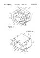
- FIG. 1is a partially cut-away isometric view of an optoelectronic connector in accordance with a first embodiment of the present invention
- FIG. 2is an isometric view of the optoelectronic connector of FIG. 1;
- FIG. 3is a cross-sectional view of the optoelectronic connector of FIG. 2;
- FIG. 4is a partially cut-away isometric view of the optoelectronic connector of FIG. 1 having a tape automated bonding (TAB) tape mounted thereon;
- TABtape automated bonding
- FIG. 5is a cross-sectional view of an optoelectronic device in accordance with a TAB embodiment of the present invention.
- FIG. 6is a cross-sectional view of an optoelectronic device in accordance with a molded contact embodiment of the present invention.
- FIG. 7is a cross-sectional view of an optoelectronic device in accordance with a flip-chip molded contact embodiment of the present invention.
- the present inventionprovides an optoelectronic device and a method for assembling the optoelectronic device.
- an optoelectronic connectoris provided.
- the optoelectronic connector and a fiber ferrulecooperate to form the optoelectronic device.
- an interconnect structureis mounted to or formed on the optoelectronic connector. Examples of the interconnect structure include a tape automated bonding (TAB) tape, flip-chip molded contacts, wire-bonded molded contacts, and the like.
- TABtape automated bonding
- optical and lightare used herein, it should be understood that these terms include all wavelengths between and including infrared and ultraviolet. It should be further understood that the same reference numerals are used in the figures to denote the same elements.
- FIG. 1is a partially cut-away isometric view of an optoelectronic connector 10 in accordance with a tape automated bonding (TAB) embodiment of the present invention.
- Optoelectronic connector 10includes a base or backwall 11 having a surface 12 and a plurality of walls 13, 14, 17, and 18 extending from base 11. Walls 13, 14, 17, and 18 cooperate to form a cavity or ferrule receiving region 19. Thus, walls 13 and 14 are opposite each other and walls 17 and 18 are opposite each other. Wall 14 has an opening 16 through which an interconnect structure (not shown) extends. Walls 17 and 18 have clips 21 for securing optoelectronic connector 10 to the ferrule.
- TABtape automated bonding
- a locator pin 23extends from wall 18 in a direction facing way from ferrule receiving cavity 19.
- another locator pin(not shown) extends from wall 14 at the intersection of wall 14 and wall 17.
- Locator pins 23mate with locator holes on a substrate (not shown) such as, for example, a printed circuit board, to position optoelectronic connector 10 on the printed circuit board. Because locator pins 23 serve to position optoelectronic connector 10 on, for example, a printed circuit board, they are also referred to as positioning features. It should be understood that locator pins 23 are optional features that are useful for positioning optoelectronic connector 10 on a substrate.
- a semiconductor receiving area 26extends from surface 12 into base 11.
- the distance semiconductor receiving area 26 extends into base 11is not a limitation of the present invention.
- semiconductor receiving area 26extends partially into base 11.
- semiconductor receiving area 26is an opening extending completely through base 11.
- semiconductor receiving area 26is a recess shaped to accept a semiconductor component.
- an interconnect recess 27extends from surface 12 into base 11, wherein interconnect recess 27 surrounds semiconductor receiving area 26.
- interconnect recess 27is a cavity having a floor 28 and walls 29. Interconnect recess 27 is also referred to as an interconnect cavity.
- semiconductor receiving area 26extends further into base 11 than does interconnect recess 27.
- Alignment pins 31protrude from floor 28 of interconnect recess 27 and extend above the plane of surface 12. Alignment pins 31 are alignment features that are used to align an optical fiber to a semiconductor component (shown in FIG. 5). A notch 36 formed in base 11 is adapted to receive a TAB tape (shown in FIG. 3).
- optoelectronic interconnect 10is a unitary structure that is formed using an injection molding process.
- optoelectronic interconnect 10is formed from a molded plastic or other low cost material.
- the type of material from which optoelectronic interconnect 10 is formedis not a limitation of the present invention.
- alignment pins 31may be formed from the molded plastic material of base 11 or they can be pins that are molded into base 11. When alignment pins 31 are molded into base 11, they may be made from metal, ceramic, or the like.
- FIG. 1further illustrates openings 20 extending through base 11. Openings 20 are optional features that simplify the structure and function of the mold used to form optoelectronic connector 10.
- optoelectronic connector 10optionally includes pick and place notches 32 that are used in cooperation with pick and place equipment to position optoelectronic connector 10 on a circuit board.
- FIG. 2is an isometric view of optoelectronic connector 10.
- the isometric view of FIG. 2further illustrates base 11, walls 13, 14, 17, and 18, cavity 19, opening 16, clips 21, locator pins 23, and pick and place notches 32.
- FIG. 2also shows a notch 15 that serves as a coarse alignment feature for a ferrule (shown in FIG. 5).
- FIG. 3is a cross-sectional view of optoelectronic connector 10 in accordance with a TAB embodiment of the present invention. What is shown in FIG. 3 is base 11 having surface 12, semiconductor receiving area 26, and interconnect recess 27 extending into base 11 from surface 12. Interconnect recess 27 has a floor 28 and walls 29. Walls 13 and 14 extend from base 11 and, in conjunction with walls 17 and 18, form cavity 19. In addition, FIG. 3 illustrates cavity 16, locator pin 23, and notches 15 and 36.
- FIG. 4is yet another partially cut-away perspective view of optoelectronic connector 10. What is shown in FIG. 4 is base 11, surface 12, walls 13, 14, 17, 18, opening 16, cavity 19, clips 21, openings 20, locator pins 23, and alignment pins 31.
- a TAB tape 33is positioned on floor 28 of interconnect recess 27 and formed or bent for interconnection with a printed circuit board (not shown). Forming or bending TAB tape 33 allows mounting optoelectronic connector 10 snugly to the printed circuit board. It should be noted that TAB tape 33 may be removably mounted to base 11 as well as bonded to base 11.
- Fiber ferrule 38having an optical fiber 39 extending therethrough is illustrated as being mated with optical connector 10, thereby forming an optoelectronic device 30.
- Fiber ferrule 38has a mating surface 41 that contacts surface 12 when fiber ferrule 38 is positioned in cavity 19.
- Fiber ferrule 38also has a rear surface 42 through which optical fiber 39 extends.
- the portion of optical fiber 39 extending from rear surface 42is typically encapsulated by a protective sheath 43 which is often referred to as a pigtail.
- fiber ferrule 38has an alignment guide 37 that mates with notch 15 to provide coarse alignment of optical fiber 39 with photonic device 35.
- Photonic device 35may be a light emitting diode, a photodetector, a laser diode, or the like.
- alignment guide 37is a rail extending from fiber ferrule 38. In other words, alignment guide 37 cooperates with notch 15 to align optical fiber 39 with photonic device 35.
- fiber ferrule 38includes a coupling cavity into which alignment pins 31 extend.
- Optoelectronic interconnect 10allows "butt-coupling" of fiber ferrule 38 with base 11, which in turn minimizes the distance between photonic device 35 and optical fiber 39 and maximizes the coupling efficiency of light transmitted between the photonic device and the optical fiber.
- the coupling efficiencyis nearly 100% when the fiber is a graded index fiber having a diameter of 62.5 micrometers ( ⁇ m), the light source is a diverging source having a half angle of 12 degrees, and the distance between photonic device 35 and optical fiber 39 is approximately 75 ⁇ m (approximately 3 mils).
- the optical or light signal from photonic device 35is identified by reference number 45 in FIG. 5.
- FIG. 5further illustrates that nearly all of the optical or light signal from photonic device 35 is transmitted to optical fiber 39.
- the coupling efficiencywill vary in accordance with the type of optical fiber, the distance between the photonic device and the optical fiber, and the type of photonic device.
- an advantage of an optoelectronic device in accordance with the TAB embodimentis that the end of optical fiber 39 may be coplanar with coupling surface 41. Moreover, mounting optoelectronic device 35 to base 11 using a TAB tape minimizes the distance between the light emitting portion of optoelectronic device 35 and optical fiber 39. For example, an end of optical fiber 39 may be positioned to be less than 125 micrometers from photonic device 35.
- fiber ferrule 38is shown as having a single optical fiber 39 extending therethrough, it should be understood this is not a limitation of the present invention. In other words, there may be a plurality of optical fibers 39 extending through fiber ferrule 38. Further, there may be a plurality of photonic devices 35 mounted to optoelectronic connector 10, wherein each optical fiber of the plurality of optical fibers is aligned with a corresponding photonic device 35 of the plurality of photonic devices. As thosed skilled in the art are aware, there are typically a plurality of photonic devices fabricated in a single semiconductor die. Thus, the plurality of optical fibers 39 are typically aligned to a single die, wherein each optical fiber of the plurality of optical fibers 39 is aligned to a single photonic device 35 of the plurality of photonic devices.
- FIG. 6is a cross-sectional view of an optoelectronic device 48 in accordance with a molded contact embodiment of the present invention.
- an optoelectronic interconnect 50that includes a base 51 having a surface 52, a semiconductor receiving area 56, and an interconnect recess 57.
- Semiconductor receiving area 56 and interconnect recess 57extend into base 51 from surface 52.
- Contacts 53 and a chip pad 55are molded into base 51 using techniques well known to those skilled in the art.
- optoelectronic interconnect 50is a unitary structure.
- a photonic device 35 having bonding pads 34is mounted on chip pad 55 in semiconductor receiving area 56.
- photonic device 35is bonded to chip pad 55 using techniques well known to those skilled in the art.
- Bonding pads 34are coupled to corresponding electrical contacts 53 using wirebonds 54.
- Wirebonds 54are manufactured such that they do not extend above surface 52, i.e, they do not "break" the plane of surface 52.
- FIG. 6further illustrates fiber ferrule 38 having an optical fiber 39 extending therethrough. Mating surface 41 of fiber ferrule 38 contacts surface 52 when fiber ferrul 38 is positioned in cavity 59. Fiber ferrule 38 has been described with reference to FIG. 3. Like optoelectronic interconnect 10, optoelectronic interconnect 50 allows "butt-coupling" of fiber ferrule 38 with base 51, which in turn minimizes the distance between photonic device 35 and optical fiber 39.
- FIG. 7is a cross-sectional view of an optoelectronic device 58 in accordance with a flip-chip molded contact embodiment of the present invention.
- an optoelectronic interconnect 60that includes a base 61 having opposing surfaces 62 and 63, a semiconductor receiving area 66, and an interconnect recess 67.
- Semiconductor receiving area 66 and interconnect recess 67extend into base 61 from surface 62.
- Contacts 64are molded into base 61 using techniques well known to those skilled in the art.
- optoelectronic interconnect 60is a unitary structure.
- a photonic device 35 having bonding pads 34is flip-chip bonded to electrical contacts 64 in semiconductor receiving area 56 using techniques well known to those skilled in the art.
- fiber ferrule 38 having an optical fiber 39 extending therethroughis also illustrated. Mating surface 41 of fiber ferrule 38 contacts surface 63 when fiber ferrule 38 is positioned in cavity 69.
- Fiber ferrule 38has been described with reference to FIG. 3.
- optoelectronic interconnect 60allows "butt-coupling" of fiber ferrule 38 with base 61, which in turn minimizes the distance between photonic device 35 and optical fiber 39.
- an optoelectronic device and a method for optically coupling an optoelectronic fiber to an optoelectronic componenthave been provided.
- a fiber connectoris directly mated or butt-coupled with a base or support structure rather than coupling the fiber connector to the support structure via an optical interface unit.
- optoelectronic devices of the present inventiondo not include optical interface units. Elimination of optical interface units lowers the cost of the optoelectronic device and increases the strength of the optical signal received by an optical detector, i.e., increases the coupling efficiency when transmitting an optical signal from an optical transmitter to an optical receiver.
- the optical interconnects of the present inventionpermit passive alignment between photonic devices and optical fibers.
Landscapes
- Physics & Mathematics (AREA)
- General Physics & Mathematics (AREA)
- Optics & Photonics (AREA)
- Optical Couplings Of Light Guides (AREA)
Abstract
Description
The present invention relates, in general, to semiconductor devices and, more particularly, to optoelectronic semiconductor devices.
Optical communications systems are comprised of light emission devices coupled to light detection devices via a plurality of optical fibers. The optical fibers are typically arranged as a bundle of fibers having a light receiving end and a light emitting end. The light receiving and emitting ends are housed in fiber ferrules. The fiber ferrule at the light receiving end of the bundle is coupled to the light emitting device via an optical interface unit. Likewise, the fiber ferrule at the light emitting end of the bundle is coupled to the light detecting device via an optical interface unit. Thus, an optical or light signal from the light emitting device is transmitted to the light detecting device through two optical interface units, two fiber ferrules, and the bundle of optical fibers.
A drawback of these systems is the large number of optical interface or coupling points through which the optical signals pass. In currently available systems, optical signals pass through at least four interfaces, i.e., interfaces between the optical interface units and the light emission and detection devices and interfaces between the optical interface units and the fiber ferrules. Each time the optical signal passes through an optical interface, a portion of the signal is lost, thereby degrading the quality of the signal received by the light detection device.
Accordingly, it would be advantageous to have a method and device for coupling or interconnecting an optical fiber to light emission and detection devices that reduces the signal loss along an optoelectronic path. It would be of further advantage for the method and device to be cost efficient and easily manufacturable.
FIG. 1 is a partially cut-away isometric view of an optoelectronic connector in accordance with a first embodiment of the present invention;
FIG. 2 is an isometric view of the optoelectronic connector of FIG. 1;
FIG. 3 is a cross-sectional view of the optoelectronic connector of FIG. 2;
FIG. 4 is a partially cut-away isometric view of the optoelectronic connector of FIG. 1 having a tape automated bonding (TAB) tape mounted thereon;
FIG. 5 is a cross-sectional view of an optoelectronic device in accordance with a TAB embodiment of the present invention;
FIG. 6 is a cross-sectional view of an optoelectronic device in accordance with a molded contact embodiment of the present invention; and
FIG. 7 is a cross-sectional view of an optoelectronic device in accordance with a flip-chip molded contact embodiment of the present invention.
Generally, the present invention provides an optoelectronic device and a method for assembling the optoelectronic device. In one aspect of the present invention, an optoelectronic connector is provided. In another aspect of the present invention, the optoelectronic connector and a fiber ferrule cooperate to form the optoelectronic device. In yet another aspect of the present invention, an interconnect structure is mounted to or formed on the optoelectronic connector. Examples of the interconnect structure include a tape automated bonding (TAB) tape, flip-chip molded contacts, wire-bonded molded contacts, and the like.
Although the terms "optical" and "light" are used herein, it should be understood that these terms include all wavelengths between and including infrared and ultraviolet. It should be further understood that the same reference numerals are used in the figures to denote the same elements.
FIG. 1 is a partially cut-away isometric view of anoptoelectronic connector 10 in accordance with a tape automated bonding (TAB) embodiment of the present invention.Optoelectronic connector 10 includes a base orbackwall 11 having asurface 12 and a plurality ofwalls base 11.Walls ferrule receiving region 19. Thus,walls walls Wall 14 has anopening 16 through which an interconnect structure (not shown) extends.Walls clips 21 for securingoptoelectronic connector 10 to the ferrule. In addition, alocator pin 23 extends fromwall 18 in a direction facing way fromferrule receiving cavity 19. Preferably, another locator pin (not shown) extends fromwall 14 at the intersection ofwall 14 andwall 17.Locator pins 23 mate with locator holes on a substrate (not shown) such as, for example, a printed circuit board, to positionoptoelectronic connector 10 on the printed circuit board. Becauselocator pins 23 serve to positionoptoelectronic connector 10 on, for example, a printed circuit board, they are also referred to as positioning features. It should be understood thatlocator pins 23 are optional features that are useful for positioningoptoelectronic connector 10 on a substrate.
Asemiconductor receiving area 26 extends fromsurface 12 intobase 11. The distancesemiconductor receiving area 26 extends intobase 11 is not a limitation of the present invention. In one example,semiconductor receiving area 26 extends partially intobase 11. In another example,semiconductor receiving area 26 is an opening extending completely throughbase 11. Preferably,semiconductor receiving area 26 is a recess shaped to accept a semiconductor component. In addition, aninterconnect recess 27 extends fromsurface 12 intobase 11, wherein interconnect recess 27 surroundssemiconductor receiving area 26. By way of example,interconnect recess 27 is a cavity having afloor 28 andwalls 29.Interconnect recess 27 is also referred to as an interconnect cavity. Preferably,semiconductor receiving area 26 extends further intobase 11 than does interconnect recess 27.
Preferably,optoelectronic interconnect 10 is a unitary structure that is formed using an injection molding process. By way of example,optoelectronic interconnect 10 is formed from a molded plastic or other low cost material. The type of material from whichoptoelectronic interconnect 10 is formed is not a limitation of the present invention. In addition,alignment pins 31 may be formed from the molded plastic material ofbase 11 or they can be pins that are molded intobase 11. Whenalignment pins 31 are molded intobase 11, they may be made from metal, ceramic, or the like.
FIG. 1 further illustratesopenings 20 extending throughbase 11.Openings 20 are optional features that simplify the structure and function of the mold used to formoptoelectronic connector 10. In addition,optoelectronic connector 10 optionally includes pick andplace notches 32 that are used in cooperation with pick and place equipment to positionoptoelectronic connector 10 on a circuit board.
FIG. 2 is an isometric view ofoptoelectronic connector 10. The isometric view of FIG. 2 further illustratesbase 11,walls cavity 19, opening 16,clips 21,locator pins 23, and pick andplace notches 32. FIG. 2 also shows anotch 15 that serves as a coarse alignment feature for a ferrule (shown in FIG. 5).
FIG. 3 is a cross-sectional view ofoptoelectronic connector 10 in accordance with a TAB embodiment of the present invention. What is shown in FIG. 3 isbase 11 havingsurface 12,semiconductor receiving area 26, andinterconnect recess 27 extending intobase 11 fromsurface 12.Interconnect recess 27 has afloor 28 andwalls 29.Walls base 11 and, in conjunction withwalls form cavity 19. In addition, FIG. 3 illustratescavity 16,locator pin 23, andnotches
FIG. 4 is yet another partially cut-away perspective view ofoptoelectronic connector 10. What is shown in FIG. 4 isbase 11,surface 12,walls cavity 19, clips 21,openings 20, locator pins 23, and alignment pins 31. In a TAB tape embodiment, aTAB tape 33 is positioned onfloor 28 ofinterconnect recess 27 and formed or bent for interconnection with a printed circuit board (not shown). Forming or bendingTAB tape 33 allows mountingoptoelectronic connector 10 snugly to the printed circuit board. It should be noted thatTAB tape 33 may be removably mounted tobase 11 as well as bonded tobase 11.
Now referring to FIG. 5, a fiber ferrule or pre-aligner 38 having anoptical fiber 39 extending therethrough is illustrated as being mated withoptical connector 10, thereby forming anoptoelectronic device 30.Fiber ferrule 38 has amating surface 41 that contacts surface 12 whenfiber ferrule 38 is positioned incavity 19.Fiber ferrule 38 also has arear surface 42 through whichoptical fiber 39 extends. The portion ofoptical fiber 39 extending fromrear surface 42 is typically encapsulated by aprotective sheath 43 which is often referred to as a pigtail. In addition,fiber ferrule 38 has analignment guide 37 that mates withnotch 15 to provide coarse alignment ofoptical fiber 39 withphotonic device 35.Photonic device 35 may be a light emitting diode, a photodetector, a laser diode, or the like. By way of example,alignment guide 37 is a rail extending fromfiber ferrule 38. In other words,alignment guide 37 cooperates withnotch 15 to alignoptical fiber 39 withphotonic device 35. Although not shown, it should be noted thatfiber ferrule 38 includes a coupling cavity into which alignment pins 31 extend.
An advantage of an optoelectronic device in accordance with the TAB embodiment is that the end ofoptical fiber 39 may be coplanar withcoupling surface 41. Moreover, mountingoptoelectronic device 35 tobase 11 using a TAB tape minimizes the distance between the light emitting portion ofoptoelectronic device 35 andoptical fiber 39. For example, an end ofoptical fiber 39 may be positioned to be less than 125 micrometers fromphotonic device 35.
Althoughfiber ferrule 38 is shown as having a singleoptical fiber 39 extending therethrough, it should be understood this is not a limitation of the present invention. In other words, there may be a plurality ofoptical fibers 39 extending throughfiber ferrule 38. Further, there may be a plurality ofphotonic devices 35 mounted tooptoelectronic connector 10, wherein each optical fiber of the plurality of optical fibers is aligned with a correspondingphotonic device 35 of the plurality of photonic devices. As thosed skilled in the art are aware, there are typically a plurality of photonic devices fabricated in a single semiconductor die. Thus, the plurality ofoptical fibers 39 are typically aligned to a single die, wherein each optical fiber of the plurality ofoptical fibers 39 is aligned to asingle photonic device 35 of the plurality of photonic devices.
FIG. 6 is a cross-sectional view of anoptoelectronic device 48 in accordance with a molded contact embodiment of the present invention. What is shown in FIG. 6 is anoptoelectronic interconnect 50 that includes a base 51 having asurface 52, asemiconductor receiving area 56, and aninterconnect recess 57.Semiconductor receiving area 56 andinterconnect recess 57 extend intobase 51 fromsurface 52.Contacts 53 and a chip pad 55 are molded intobase 51 using techniques well known to those skilled in the art. Preferably,optoelectronic interconnect 50 is a unitary structure. Aphotonic device 35 havingbonding pads 34 is mounted on chip pad 55 insemiconductor receiving area 56. Preferably,photonic device 35 is bonded to chip pad 55 using techniques well known to those skilled in the art.Bonding pads 34 are coupled to correspondingelectrical contacts 53 usingwirebonds 54.Wirebonds 54 are manufactured such that they do not extend abovesurface 52, i.e, they do not "break" the plane ofsurface 52.
FIG. 6 further illustratesfiber ferrule 38 having anoptical fiber 39 extending therethrough.Mating surface 41 offiber ferrule 38 contacts surface 52 whenfiber ferrul 38 is positioned incavity 59.Fiber ferrule 38 has been described with reference to FIG. 3. Likeoptoelectronic interconnect 10,optoelectronic interconnect 50 allows "butt-coupling" offiber ferrule 38 withbase 51, which in turn minimizes the distance betweenphotonic device 35 andoptical fiber 39.
FIG. 7 is a cross-sectional view of anoptoelectronic device 58 in accordance with a flip-chip molded contact embodiment of the present invention. What is shown in FIG. 7 is anoptoelectronic interconnect 60 that includes a base 61 having opposingsurfaces semiconductor receiving area 66, and aninterconnect recess 67.Semiconductor receiving area 66 andinterconnect recess 67 extend intobase 61 fromsurface 62.Contacts 64 are molded intobase 61 using techniques well known to those skilled in the art. Preferably,optoelectronic interconnect 60 is a unitary structure. Aphotonic device 35 havingbonding pads 34 is flip-chip bonded toelectrical contacts 64 insemiconductor receiving area 56 using techniques well known to those skilled in the art.
Still referring to FIG. 7,fiber ferrule 38 having anoptical fiber 39 extending therethrough is also illustrated.Mating surface 41 offiber ferrule 38 contacts surface 63 whenfiber ferrule 38 is positioned incavity 69.Fiber ferrule 38 has been described with reference to FIG. 3. Likeoptoelectronic interconnect 10,optoelectronic interconnect 60 allows "butt-coupling" offiber ferrule 38 withbase 61, which in turn minimizes the distance betweenphotonic device 35 andoptical fiber 39.
By now it should be appreciated that an optoelectronic device and a method for optically coupling an optoelectronic fiber to an optoelectronic component have been provided. In accordance with the present invention, a fiber connector is directly mated or butt-coupled with a base or support structure rather than coupling the fiber connector to the support structure via an optical interface unit. Thus, optoelectronic devices of the present invention do not include optical interface units. Elimination of optical interface units lowers the cost of the optoelectronic device and increases the strength of the optical signal received by an optical detector, i.e., increases the coupling efficiency when transmitting an optical signal from an optical transmitter to an optical receiver. In addition, the optical interconnects of the present invention permit passive alignment between photonic devices and optical fibers.
Claims (20)
1. An optoelectronic device, comprising:
a base having a support wall, the support wall having a first surface;
first and second walls extending from the support wall, the first and second walls opposite one another;
a third wall extending from the support wall, the third wall in contact with the first and second walls;
a fourth wall spaced apart from the support wall and in contact with the first and second walls such that an opening is between the fourth wall and the support wall, and wherein the support, first, second, third, and fourth walls cooperate to form a cavity;
a recess in the support wall, the recess having a second surface;
a semiconductor component receiving area extending from the second surface into the support wall;
a first alignment feature extending from the base; and
a semiconductor component located in the semiconductor component receiving area.
2. The optoelectronic device of claim 1, further including a ferrule having a mating surface and an optical fiber extending therethrough.
3. The optoelectronic device of claim 2, wherein the semiconductor component is a photonic device.
4. The optoelectronic device of claim 1, further including an interconnect cavity extending from the second surface into the support wall, wherein the interconnect cavity is adjacent the semiconductor component receiving area.
5. The optoelectronic device of claim 4, further including a tape automated bonding (TAB) tape located in the interconnect cavity, wherein the semiconductor component is bonded to the TAB tape.
6. The optoelectronic device of claim 4, further including electrical contacts in the base, wherein the semiconductor component is flip-chip bonded to the electrical contacts.
7. The optoelectronic device of claim 4, further including electrical contacts in the base, wherein the semiconductor component is wire bonded to the electrical contacts.
8. An optoelectronic connector, comprising:
a base having a first surface, wherein a recess extends from the first surface into the base, the recess having recess walls, a floor, and a semiconductor component receiving area extending from the floor into the base;
a first wall extending from a first portion of the first surface and terminating with a first clip;
a second wall extending from a second portion of the first surface and terminating with a second clip, the first and second walls facing one another;
a third wall extending from a third portion of the first surface, the third wall coupling the first wall to the second wall;
a fourth wall spaced apart from the first surface and coupling the first wall to the second wall, the third and fourth walls substantially parallel to each other, wherein the first, second, third, and fourth walls cooperate to form a cavity; and
a first alignment feature extending from the floor.
9. The optoelectronic connector of claim 8, wherein the optoelectronic connector is a unitary structure.
10. The optoelectronic connector of claim 9, wherein the optoelectronic connector is plastic.
11. The optoelectronic connector of claim 8, further including
a second alignment feature extending into the third wall.
12. The optoelectronic connector of claim 11, further including
a positioning feature protruding from one of the third and fourth walls, wherein the positioning feature protrudes in a direction facing away from the cavity.
13. The optoelectronic connector of claim 8, further including an interconnect recess extending from the surface into the base, wherein the interconnect recess is adjacent the recess walls.
14. The optoelectronic connector of claim 13, further including a tape automated bonding (TAB) tape located in the interconnect recess.
15. The optoelectronic connector of claim 13, further including electrical contacts located in the interconnect recess.
16. The optoelectronic connector of claim 8, wherein the first alignment feature includes a plurality of alignment pins molded into the base.
17. A method for assembling an optoelectronic device, comprising the steps of:
mounting an optoelectronic component to an optoelectronic connector comprising:
a base having a first surface, wherein a recess extends from the first surface into the base, the recess having recess walls, a floor, and a semiconductor component receiving area extending from the floor into the base;
a first wall extending from a first portion of the first surface and terminating with a first clip;
a second wall extending from a second portion of the first surface and terminating with a second clip, the first and second walls facing one another;
a third wall extending from a third portion of the first surface, the third wall coupling the first wall to the second wall;
a fourth wall spaced apart from the first surface and coupling the first wall to the second wall, the third and fourth walls substantially parallel to each other, wherein the first, second, third, and fourth walls cooperate to form a cavity; and
an alignment feature extending from the floor;
coupling an optical fiber to a fiber connector; and
directly coupling the fiber connector to the optoelectronic connector, wherein an end of the optical fiber is spaced apart from the optoelectronic component.
18. The method of claim 17, wherein the step of mounting an optoelectronic component to an optoelectronic connector includes mounting the optoelectronic component to a tape automated bonded (TAB) tape and mounting the TAB tape to the fiber connector.
19. The method of claim 17, wherein the step of directly coupling the fiber connector to the optoelectronic connector includes positioning an end of the optical fiber to be less than approximately 125 micrometers from the optoelectronic component.
20. The method of claim 17, further including the step of forming a molded contact in the optoelectronic connector and wherein the step of directly coupling the fiber connector to the optoelectronic connector includes mounting the optoelectronic component on the molded contact.
Priority Applications (1)
| Application Number | Priority Date | Filing Date | Title |
|---|---|---|---|
| US08/861,880US5933558A (en) | 1997-05-22 | 1997-05-22 | Optoelectronic device and method of assembly |
Applications Claiming Priority (1)
| Application Number | Priority Date | Filing Date | Title |
|---|---|---|---|
| US08/861,880US5933558A (en) | 1997-05-22 | 1997-05-22 | Optoelectronic device and method of assembly |
Publications (1)
| Publication Number | Publication Date |
|---|---|
| US5933558Atrue US5933558A (en) | 1999-08-03 |
Family
ID=25337017
Family Applications (1)
| Application Number | Title | Priority Date | Filing Date |
|---|---|---|---|
| US08/861,880Expired - LifetimeUS5933558A (en) | 1997-05-22 | 1997-05-22 | Optoelectronic device and method of assembly |
Country Status (1)
| Country | Link |
|---|---|
| US (1) | US5933558A (en) |
Cited By (63)
| Publication number | Priority date | Publication date | Assignee | Title |
|---|---|---|---|---|
| US6056448A (en)* | 1998-04-16 | 2000-05-02 | Lockheed Martin Corporation | Vertical cavity surface emitting laser array packaging |
| US6206581B1 (en)* | 1999-10-06 | 2001-03-27 | Lucent Technologies Inc. | Optical connector having a one-piece housing |
| US6318909B1 (en)* | 1999-02-11 | 2001-11-20 | Agilent Technologies, Inc. | Integrated packaging system for optical communications devices that provides automatic alignment with optical fibers |
| US20030026556A1 (en)* | 2001-08-03 | 2003-02-06 | National Semiconductor Corporation | Optical sub-assembly for optoelectronic modules |
| US20030057535A1 (en)* | 2001-09-24 | 2003-03-27 | National Semiconductor Corporation | Techniques for attaching rotated photonic devices to an optical sub-assembly in an optoelectronic package |
| US6583902B1 (en) | 1999-12-09 | 2003-06-24 | Alvesta, Inc. | Modular fiber-optic transceiver |
| US20040005124A1 (en)* | 2002-06-17 | 2004-01-08 | Kendra Gallup | Actively aligned optoelectronic device |
| US20040047571A1 (en)* | 2002-09-06 | 2004-03-11 | Boord Warren Timothy | Hermetically sealed ferrule |
| US6830382B1 (en)* | 2001-12-20 | 2004-12-14 | National Semiconductor Corporation | Miniature form-factor connecter for fiber optic modules |
| US20040264866A1 (en)* | 2000-10-25 | 2004-12-30 | Sherrer David W. | Wafer level packaging for optoelectronic devices |
| US20050013560A1 (en)* | 2003-07-15 | 2005-01-20 | National Semiconductor Corporation | Opto-electronic module form factor having adjustable optical plane height |
| US6883977B2 (en) | 2000-12-14 | 2005-04-26 | Shipley Company, L.L.C. | Optical device package for flip-chip mounting |
| US20050169644A1 (en)* | 2003-11-14 | 2005-08-04 | Fuji Xerox Co., Ltd. | Optical signal transmitting device |
| US6932519B2 (en) | 2000-11-16 | 2005-08-23 | Shipley Company, L.L.C. | Optical device package |
| US7023705B2 (en) | 2001-08-03 | 2006-04-04 | National Semiconductor Corporation | Ceramic optical sub-assembly for optoelectronic modules |
| US20060140534A1 (en)* | 2001-08-03 | 2006-06-29 | National Semiconductor Corporation | Ceramic optical sub-assembly for optoelectronic modules |
| US20100215320A1 (en)* | 2009-02-24 | 2010-08-26 | Avago Technologies Fiber Ip (Singapore) Pte. Ltd. | Molded interconnect device (mid) optical connector with metal retaining clip |
| WO2011002712A1 (en)* | 2009-06-29 | 2011-01-06 | Hsio Technologies, Llc | Singulated semiconductor device separable electrical interconnect |
| US20130071064A1 (en)* | 2010-04-30 | 2013-03-21 | Paul Kessler Rosenberg | Device for converting signal |
| US20130202255A1 (en)* | 2012-02-01 | 2013-08-08 | Cisco Technology, Inc. | Single Mode Fiber Array Connector For Opto-Electronic Transceivers |
| US8525346B2 (en) | 2009-06-02 | 2013-09-03 | Hsio Technologies, Llc | Compliant conductive nano-particle electrical interconnect |
| US8610265B2 (en) | 2009-06-02 | 2013-12-17 | Hsio Technologies, Llc | Compliant core peripheral lead semiconductor test socket |
| US8618649B2 (en) | 2009-06-02 | 2013-12-31 | Hsio Technologies, Llc | Compliant printed circuit semiconductor package |
| US8758067B2 (en) | 2010-06-03 | 2014-06-24 | Hsio Technologies, Llc | Selective metalization of electrical connector or socket housing |
| US8789272B2 (en) | 2009-06-02 | 2014-07-29 | Hsio Technologies, Llc | Method of making a compliant printed circuit peripheral lead semiconductor test socket |
| US8803539B2 (en) | 2009-06-03 | 2014-08-12 | Hsio Technologies, Llc | Compliant wafer level probe assembly |
| US8912812B2 (en) | 2009-06-02 | 2014-12-16 | Hsio Technologies, Llc | Compliant printed circuit wafer probe diagnostic tool |
| US8928344B2 (en) | 2009-06-02 | 2015-01-06 | Hsio Technologies, Llc | Compliant printed circuit socket diagnostic tool |
| US8955215B2 (en) | 2009-05-28 | 2015-02-17 | Hsio Technologies, Llc | High performance surface mount electrical interconnect |
| US8955216B2 (en) | 2009-06-02 | 2015-02-17 | Hsio Technologies, Llc | Method of making a compliant printed circuit peripheral lead semiconductor package |
| US8970031B2 (en) | 2009-06-16 | 2015-03-03 | Hsio Technologies, Llc | Semiconductor die terminal |
| US8981809B2 (en) | 2009-06-29 | 2015-03-17 | Hsio Technologies, Llc | Compliant printed circuit semiconductor tester interface |
| US8981568B2 (en) | 2009-06-16 | 2015-03-17 | Hsio Technologies, Llc | Simulated wirebond semiconductor package |
| US8988093B2 (en) | 2009-06-02 | 2015-03-24 | Hsio Technologies, Llc | Bumped semiconductor wafer or die level electrical interconnect |
| US8987886B2 (en) | 2009-06-02 | 2015-03-24 | Hsio Technologies, Llc | Copper pillar full metal via electrical circuit structure |
| US9054097B2 (en) | 2009-06-02 | 2015-06-09 | Hsio Technologies, Llc | Compliant printed circuit area array semiconductor device package |
| US9093767B2 (en) | 2009-06-02 | 2015-07-28 | Hsio Technologies, Llc | High performance surface mount electrical interconnect |
| US9136196B2 (en) | 2009-06-02 | 2015-09-15 | Hsio Technologies, Llc | Compliant printed circuit wafer level semiconductor package |
| US9184527B2 (en) | 2009-06-02 | 2015-11-10 | Hsio Technologies, Llc | Electrical connector insulator housing |
| US9184145B2 (en) | 2009-06-02 | 2015-11-10 | Hsio Technologies, Llc | Semiconductor device package adapter |
| US9196980B2 (en) | 2009-06-02 | 2015-11-24 | Hsio Technologies, Llc | High performance surface mount electrical interconnect with external biased normal force loading |
| US9231328B2 (en) | 2009-06-02 | 2016-01-05 | Hsio Technologies, Llc | Resilient conductive electrical interconnect |
| US9232654B2 (en) | 2009-06-02 | 2016-01-05 | Hsio Technologies, Llc | High performance electrical circuit structure |
| US9276339B2 (en) | 2009-06-02 | 2016-03-01 | Hsio Technologies, Llc | Electrical interconnect IC device socket |
| US9277654B2 (en) | 2009-06-02 | 2016-03-01 | Hsio Technologies, Llc | Composite polymer-metal electrical contacts |
| US9276336B2 (en) | 2009-05-28 | 2016-03-01 | Hsio Technologies, Llc | Metalized pad to electrical contact interface |
| US9320144B2 (en) | 2009-06-17 | 2016-04-19 | Hsio Technologies, Llc | Method of forming a semiconductor socket |
| US9320133B2 (en) | 2009-06-02 | 2016-04-19 | Hsio Technologies, Llc | Electrical interconnect IC device socket |
| US9318862B2 (en) | 2009-06-02 | 2016-04-19 | Hsio Technologies, Llc | Method of making an electronic interconnect |
| US9350093B2 (en) | 2010-06-03 | 2016-05-24 | Hsio Technologies, Llc | Selective metalization of electrical connector or socket housing |
| US9414500B2 (en) | 2009-06-02 | 2016-08-09 | Hsio Technologies, Llc | Compliant printed flexible circuit |
| US9536815B2 (en) | 2009-05-28 | 2017-01-03 | Hsio Technologies, Llc | Semiconductor socket with direct selective metalization |
| US9559447B2 (en) | 2015-03-18 | 2017-01-31 | Hsio Technologies, Llc | Mechanical contact retention within an electrical connector |
| US9603249B2 (en) | 2009-06-02 | 2017-03-21 | Hsio Technologies, Llc | Direct metalization of electrical circuit structures |
| US9613841B2 (en) | 2009-06-02 | 2017-04-04 | Hsio Technologies, Llc | Area array semiconductor device package interconnect structure with optional package-to-package or flexible circuit to package connection |
| US9689897B2 (en) | 2010-06-03 | 2017-06-27 | Hsio Technologies, Llc | Performance enhanced semiconductor socket |
| US20170181604A1 (en)* | 2014-03-17 | 2017-06-29 | Intuitive Surgical Operations, Inc. | Multi-stage instrument connector |
| US9699906B2 (en) | 2009-06-02 | 2017-07-04 | Hsio Technologies, Llc | Hybrid printed circuit assembly with low density main core and embedded high density circuit regions |
| US9761520B2 (en) | 2012-07-10 | 2017-09-12 | Hsio Technologies, Llc | Method of making an electrical connector having electrodeposited terminals |
| US9930775B2 (en) | 2009-06-02 | 2018-03-27 | Hsio Technologies, Llc | Copper pillar full metal via electrical circuit structure |
| US10159154B2 (en) | 2010-06-03 | 2018-12-18 | Hsio Technologies, Llc | Fusion bonded liquid crystal polymer circuit structure |
| US10506722B2 (en) | 2013-07-11 | 2019-12-10 | Hsio Technologies, Llc | Fusion bonded liquid crystal polymer electrical circuit structure |
| US10667410B2 (en) | 2013-07-11 | 2020-05-26 | Hsio Technologies, Llc | Method of making a fusion bonded circuit structure |
Citations (21)
| Publication number | Priority date | Publication date | Assignee | Title |
|---|---|---|---|---|
| US3846010A (en)* | 1973-07-05 | 1974-11-05 | Corning Glass Works | Optical waveguide connector |
| US4357072A (en)* | 1978-01-28 | 1982-11-02 | Plessey Handel Und Investments Ag | Sealing optical fibres into packages |
| US4943136A (en)* | 1988-12-09 | 1990-07-24 | The Boeing Company | Optical backplane interconnection |
| US5093879A (en)* | 1990-06-22 | 1992-03-03 | International Business Machines Corporation | Electro-optical connectors |
| US5175790A (en)* | 1989-04-13 | 1992-12-29 | Hoechst Aktiengesellschaft | Transparent thermoplastic molding compound made of 2,3-difluoroacrylic acid esters |
| US5202943A (en)* | 1991-10-04 | 1993-04-13 | International Business Machines Corporation | Optoelectronic assembly with alignment member |
| US5228101A (en)* | 1992-03-02 | 1993-07-13 | Motorola, Inc. | Electrical to optical links using metalization |
| US5230030A (en)* | 1992-04-24 | 1993-07-20 | Motorola, Inc. | Interface coupling electronic circuitry |
| US5259053A (en)* | 1992-06-29 | 1993-11-02 | The Whitaker Corporation | Discrete optical receptacle assembly with alignment feature |
| US5276754A (en)* | 1992-07-06 | 1994-01-04 | Motorola, Inc. | Optoelectronic mount and method for making |
| US5337391A (en)* | 1993-05-03 | 1994-08-09 | Motorola, Inc. | Optoelectronic sub-module and method of making same |
| US5345527A (en)* | 1993-09-03 | 1994-09-06 | Motorola, Inc. | Intelligent opto-bus with display |
| US5359686A (en)* | 1993-03-29 | 1994-10-25 | Motorola, Inc. | Interface for coupling optical fibers to electronic circuitry |
| US5389312A (en)* | 1993-10-26 | 1995-02-14 | Motorola, Inc. | Method of fabricating molded optical waveguides |
| US5416872A (en)* | 1993-07-06 | 1995-05-16 | At&T Corp. | Arrangement for interconnecting an optical fiber an optoelectronic component |
| US5420954A (en)* | 1993-05-24 | 1995-05-30 | Photonics Research Incorporated | Parallel optical interconnect |
| US5432630A (en)* | 1992-09-11 | 1995-07-11 | Motorola, Inc. | Optical bus with optical transceiver modules and method of manufacture |
| US5473716A (en)* | 1994-08-29 | 1995-12-05 | Motorola, Inc. | Fiber bundle interconnect and method of making same |
| US5548677A (en)* | 1993-03-31 | 1996-08-20 | Sumitomo Electric Industries, Ltd. | Housing structure for coupling and releasing optical modules |
| US5768456A (en)* | 1996-11-22 | 1998-06-16 | Motorola, Inc. | Optoelectronic package including photonic device mounted in flexible substrate |
| US5781682A (en)* | 1996-02-01 | 1998-07-14 | International Business Machines Corporation | Low-cost packaging for parallel optical computer link |
- 1997
- 1997-05-22USUS08/861,880patent/US5933558A/ennot_activeExpired - Lifetime
Patent Citations (21)
| Publication number | Priority date | Publication date | Assignee | Title |
|---|---|---|---|---|
| US3846010A (en)* | 1973-07-05 | 1974-11-05 | Corning Glass Works | Optical waveguide connector |
| US4357072A (en)* | 1978-01-28 | 1982-11-02 | Plessey Handel Und Investments Ag | Sealing optical fibres into packages |
| US4943136A (en)* | 1988-12-09 | 1990-07-24 | The Boeing Company | Optical backplane interconnection |
| US5175790A (en)* | 1989-04-13 | 1992-12-29 | Hoechst Aktiengesellschaft | Transparent thermoplastic molding compound made of 2,3-difluoroacrylic acid esters |
| US5093879A (en)* | 1990-06-22 | 1992-03-03 | International Business Machines Corporation | Electro-optical connectors |
| US5202943A (en)* | 1991-10-04 | 1993-04-13 | International Business Machines Corporation | Optoelectronic assembly with alignment member |
| US5228101A (en)* | 1992-03-02 | 1993-07-13 | Motorola, Inc. | Electrical to optical links using metalization |
| US5230030A (en)* | 1992-04-24 | 1993-07-20 | Motorola, Inc. | Interface coupling electronic circuitry |
| US5259053A (en)* | 1992-06-29 | 1993-11-02 | The Whitaker Corporation | Discrete optical receptacle assembly with alignment feature |
| US5276754A (en)* | 1992-07-06 | 1994-01-04 | Motorola, Inc. | Optoelectronic mount and method for making |
| US5432630A (en)* | 1992-09-11 | 1995-07-11 | Motorola, Inc. | Optical bus with optical transceiver modules and method of manufacture |
| US5359686A (en)* | 1993-03-29 | 1994-10-25 | Motorola, Inc. | Interface for coupling optical fibers to electronic circuitry |
| US5548677A (en)* | 1993-03-31 | 1996-08-20 | Sumitomo Electric Industries, Ltd. | Housing structure for coupling and releasing optical modules |
| US5337391A (en)* | 1993-05-03 | 1994-08-09 | Motorola, Inc. | Optoelectronic sub-module and method of making same |
| US5420954A (en)* | 1993-05-24 | 1995-05-30 | Photonics Research Incorporated | Parallel optical interconnect |
| US5416872A (en)* | 1993-07-06 | 1995-05-16 | At&T Corp. | Arrangement for interconnecting an optical fiber an optoelectronic component |
| US5345527A (en)* | 1993-09-03 | 1994-09-06 | Motorola, Inc. | Intelligent opto-bus with display |
| US5389312A (en)* | 1993-10-26 | 1995-02-14 | Motorola, Inc. | Method of fabricating molded optical waveguides |
| US5473716A (en)* | 1994-08-29 | 1995-12-05 | Motorola, Inc. | Fiber bundle interconnect and method of making same |
| US5781682A (en)* | 1996-02-01 | 1998-07-14 | International Business Machines Corporation | Low-cost packaging for parallel optical computer link |
| US5768456A (en)* | 1996-11-22 | 1998-06-16 | Motorola, Inc. | Optoelectronic package including photonic device mounted in flexible substrate |
Non-Patent Citations (2)
| Title |
|---|
| "Plastic-Based Receptacle-Type VCSEL-Array Modules with One and Two Dimensions Fabricated Using the Self-Alighnment Technique" Kosaka, Kajita, Yamada, Sugimoto, Kurata, Tanabe and Kasukawa, 1997 Proceedings 47th Electronic Components & Technology Conference May 18-21, 1997, San Jose, California, pp. 382-390. |
| Plastic Based Receptacle Type VCSEL Array Modules with One and Two Dimensions Fabricated Using the Self Alighnment Technique Kosaka, Kajita, Yamada, Sugimoto, Kurata, Tanabe and Kasukawa, 1997 Proceedings 47th Electronic Components & Technology Conference May 18 21, 1997, San Jose, California, pp. 382 390.* |
Cited By (90)
| Publication number | Priority date | Publication date | Assignee | Title |
|---|---|---|---|---|
| US6056448A (en)* | 1998-04-16 | 2000-05-02 | Lockheed Martin Corporation | Vertical cavity surface emitting laser array packaging |
| US6318909B1 (en)* | 1999-02-11 | 2001-11-20 | Agilent Technologies, Inc. | Integrated packaging system for optical communications devices that provides automatic alignment with optical fibers |
| US20020021874A1 (en)* | 1999-02-11 | 2002-02-21 | Giboney Kirk S. | Integrated packaging system for optical communications devices that provides automatic alignment with optical fibers |
| US20060008214A1 (en)* | 1999-02-11 | 2006-01-12 | Giboney Kirk S | Integrated packaging system for optical communications devices that provides automatic alignment with optical fibers |
| US6835003B2 (en) | 1999-02-11 | 2004-12-28 | Agilent Technologies, Inc. | Integrated packaging system for optical communications devices that provides automatic alignment with optical fibers |
| US7380994B2 (en) | 1999-02-11 | 2008-06-03 | Avago Technologies Fiber Ip Pte Ltd | Integrated packaging system for optical communications devices that provides automatic alignment with optical fibers |
| US6293710B1 (en) | 1999-10-06 | 2001-09-25 | Lucent Technologies Inc. | Optical connector having a one-piece housing |
| US6206581B1 (en)* | 1999-10-06 | 2001-03-27 | Lucent Technologies Inc. | Optical connector having a one-piece housing |
| US6583902B1 (en) | 1999-12-09 | 2003-06-24 | Alvesta, Inc. | Modular fiber-optic transceiver |
| US7345316B2 (en) | 2000-10-25 | 2008-03-18 | Shipley Company, L.L.C. | Wafer level packaging for optoelectronic devices |
| US20040264866A1 (en)* | 2000-10-25 | 2004-12-30 | Sherrer David W. | Wafer level packaging for optoelectronic devices |
| US6932519B2 (en) | 2000-11-16 | 2005-08-23 | Shipley Company, L.L.C. | Optical device package |
| US7246953B2 (en) | 2000-11-16 | 2007-07-24 | Shipley Company, L.L.C. | Optical device package |
| US6883977B2 (en) | 2000-12-14 | 2005-04-26 | Shipley Company, L.L.C. | Optical device package for flip-chip mounting |
| US7086788B2 (en) | 2001-08-03 | 2006-08-08 | National Semiconductor Corporation | Optical sub-assembly for opto-electronic modules |
| US6916121B2 (en) | 2001-08-03 | 2005-07-12 | National Semiconductor Corporation | Optical sub-assembly for optoelectronic modules |
| US7269027B2 (en) | 2001-08-03 | 2007-09-11 | National Semiconductor Corporation | Ceramic optical sub-assembly for optoelectronic modules |
| US20030026556A1 (en)* | 2001-08-03 | 2003-02-06 | National Semiconductor Corporation | Optical sub-assembly for optoelectronic modules |
| US20060140534A1 (en)* | 2001-08-03 | 2006-06-29 | National Semiconductor Corporation | Ceramic optical sub-assembly for optoelectronic modules |
| US7023705B2 (en) | 2001-08-03 | 2006-04-04 | National Semiconductor Corporation | Ceramic optical sub-assembly for optoelectronic modules |
| US20030057535A1 (en)* | 2001-09-24 | 2003-03-27 | National Semiconductor Corporation | Techniques for attaching rotated photonic devices to an optical sub-assembly in an optoelectronic package |
| US6973225B2 (en) | 2001-09-24 | 2005-12-06 | National Semiconductor Corporation | Techniques for attaching rotated photonic devices to an optical sub-assembly in an optoelectronic package |
| US6830382B1 (en)* | 2001-12-20 | 2004-12-14 | National Semiconductor Corporation | Miniature form-factor connecter for fiber optic modules |
| US6955480B2 (en) | 2002-06-17 | 2005-10-18 | Agilent Technologies, Inc. | Actively aligned optoelectronic device |
| US20040005124A1 (en)* | 2002-06-17 | 2004-01-08 | Kendra Gallup | Actively aligned optoelectronic device |
| US20040047571A1 (en)* | 2002-09-06 | 2004-03-11 | Boord Warren Timothy | Hermetically sealed ferrule |
| US7156562B2 (en) | 2003-07-15 | 2007-01-02 | National Semiconductor Corporation | Opto-electronic module form factor having adjustable optical plane height |
| US20050013560A1 (en)* | 2003-07-15 | 2005-01-20 | National Semiconductor Corporation | Opto-electronic module form factor having adjustable optical plane height |
| US20050169644A1 (en)* | 2003-11-14 | 2005-08-04 | Fuji Xerox Co., Ltd. | Optical signal transmitting device |
| US20100215320A1 (en)* | 2009-02-24 | 2010-08-26 | Avago Technologies Fiber Ip (Singapore) Pte. Ltd. | Molded interconnect device (mid) optical connector with metal retaining clip |
| US7963705B2 (en)* | 2009-02-24 | 2011-06-21 | Avago Technologies Fiber Ip (Singapore) Pte. Ltd. | Molded interconnect device (MID) optical connector with metal retaining clip |
| US9660368B2 (en) | 2009-05-28 | 2017-05-23 | Hsio Technologies, Llc | High performance surface mount electrical interconnect |
| US9536815B2 (en) | 2009-05-28 | 2017-01-03 | Hsio Technologies, Llc | Semiconductor socket with direct selective metalization |
| US9276336B2 (en) | 2009-05-28 | 2016-03-01 | Hsio Technologies, Llc | Metalized pad to electrical contact interface |
| US8955215B2 (en) | 2009-05-28 | 2015-02-17 | Hsio Technologies, Llc | High performance surface mount electrical interconnect |
| US8928344B2 (en) | 2009-06-02 | 2015-01-06 | Hsio Technologies, Llc | Compliant printed circuit socket diagnostic tool |
| US9613841B2 (en) | 2009-06-02 | 2017-04-04 | Hsio Technologies, Llc | Area array semiconductor device package interconnect structure with optional package-to-package or flexible circuit to package connection |
| US8704377B2 (en) | 2009-06-02 | 2014-04-22 | Hsio Technologies, Llc | Compliant conductive nano-particle electrical interconnect |
| US10609819B2 (en) | 2009-06-02 | 2020-03-31 | Hsio Technologies, Llc | Hybrid printed circuit assembly with low density main core and embedded high density circuit regions |
| US8789272B2 (en) | 2009-06-02 | 2014-07-29 | Hsio Technologies, Llc | Method of making a compliant printed circuit peripheral lead semiconductor test socket |
| US9930775B2 (en) | 2009-06-02 | 2018-03-27 | Hsio Technologies, Llc | Copper pillar full metal via electrical circuit structure |
| US8829671B2 (en) | 2009-06-02 | 2014-09-09 | Hsio Technologies, Llc | Compliant core peripheral lead semiconductor socket |
| US8912812B2 (en) | 2009-06-02 | 2014-12-16 | Hsio Technologies, Llc | Compliant printed circuit wafer probe diagnostic tool |
| US8610265B2 (en) | 2009-06-02 | 2013-12-17 | Hsio Technologies, Llc | Compliant core peripheral lead semiconductor test socket |
| US8525346B2 (en) | 2009-06-02 | 2013-09-03 | Hsio Technologies, Llc | Compliant conductive nano-particle electrical interconnect |
| US8955216B2 (en) | 2009-06-02 | 2015-02-17 | Hsio Technologies, Llc | Method of making a compliant printed circuit peripheral lead semiconductor package |
| US9699906B2 (en) | 2009-06-02 | 2017-07-04 | Hsio Technologies, Llc | Hybrid printed circuit assembly with low density main core and embedded high density circuit regions |
| US8618649B2 (en) | 2009-06-02 | 2013-12-31 | Hsio Technologies, Llc | Compliant printed circuit semiconductor package |
| US9603249B2 (en) | 2009-06-02 | 2017-03-21 | Hsio Technologies, Llc | Direct metalization of electrical circuit structures |
| US9414500B2 (en) | 2009-06-02 | 2016-08-09 | Hsio Technologies, Llc | Compliant printed flexible circuit |
| US8988093B2 (en) | 2009-06-02 | 2015-03-24 | Hsio Technologies, Llc | Bumped semiconductor wafer or die level electrical interconnect |
| US8987886B2 (en) | 2009-06-02 | 2015-03-24 | Hsio Technologies, Llc | Copper pillar full metal via electrical circuit structure |
| US9054097B2 (en) | 2009-06-02 | 2015-06-09 | Hsio Technologies, Llc | Compliant printed circuit area array semiconductor device package |
| US9076884B2 (en) | 2009-06-02 | 2015-07-07 | Hsio Technologies, Llc | Compliant printed circuit semiconductor package |
| US9093767B2 (en) | 2009-06-02 | 2015-07-28 | Hsio Technologies, Llc | High performance surface mount electrical interconnect |
| US9136196B2 (en) | 2009-06-02 | 2015-09-15 | Hsio Technologies, Llc | Compliant printed circuit wafer level semiconductor package |
| US9184527B2 (en) | 2009-06-02 | 2015-11-10 | Hsio Technologies, Llc | Electrical connector insulator housing |
| US9184145B2 (en) | 2009-06-02 | 2015-11-10 | Hsio Technologies, Llc | Semiconductor device package adapter |
| US9196980B2 (en) | 2009-06-02 | 2015-11-24 | Hsio Technologies, Llc | High performance surface mount electrical interconnect with external biased normal force loading |
| US9231328B2 (en) | 2009-06-02 | 2016-01-05 | Hsio Technologies, Llc | Resilient conductive electrical interconnect |
| US9232654B2 (en) | 2009-06-02 | 2016-01-05 | Hsio Technologies, Llc | High performance electrical circuit structure |
| US9276339B2 (en) | 2009-06-02 | 2016-03-01 | Hsio Technologies, Llc | Electrical interconnect IC device socket |
| US9277654B2 (en) | 2009-06-02 | 2016-03-01 | Hsio Technologies, Llc | Composite polymer-metal electrical contacts |
| US9318862B2 (en) | 2009-06-02 | 2016-04-19 | Hsio Technologies, Llc | Method of making an electronic interconnect |
| US9320133B2 (en) | 2009-06-02 | 2016-04-19 | Hsio Technologies, Llc | Electrical interconnect IC device socket |
| US8803539B2 (en) | 2009-06-03 | 2014-08-12 | Hsio Technologies, Llc | Compliant wafer level probe assembly |
| US8981568B2 (en) | 2009-06-16 | 2015-03-17 | Hsio Technologies, Llc | Simulated wirebond semiconductor package |
| US8970031B2 (en) | 2009-06-16 | 2015-03-03 | Hsio Technologies, Llc | Semiconductor die terminal |
| US9320144B2 (en) | 2009-06-17 | 2016-04-19 | Hsio Technologies, Llc | Method of forming a semiconductor socket |
| US8984748B2 (en) | 2009-06-29 | 2015-03-24 | Hsio Technologies, Llc | Singulated semiconductor device separable electrical interconnect |
| WO2011002712A1 (en)* | 2009-06-29 | 2011-01-06 | Hsio Technologies, Llc | Singulated semiconductor device separable electrical interconnect |
| US8981809B2 (en) | 2009-06-29 | 2015-03-17 | Hsio Technologies, Llc | Compliant printed circuit semiconductor tester interface |
| US9297967B2 (en)* | 2010-04-30 | 2016-03-29 | Hewlett Packard Enterprise Development Lp | Device for converting signal |
| US20130071064A1 (en)* | 2010-04-30 | 2013-03-21 | Paul Kessler Rosenberg | Device for converting signal |
| US10159154B2 (en) | 2010-06-03 | 2018-12-18 | Hsio Technologies, Llc | Fusion bonded liquid crystal polymer circuit structure |
| US9689897B2 (en) | 2010-06-03 | 2017-06-27 | Hsio Technologies, Llc | Performance enhanced semiconductor socket |
| US8758067B2 (en) | 2010-06-03 | 2014-06-24 | Hsio Technologies, Llc | Selective metalization of electrical connector or socket housing |
| US9350093B2 (en) | 2010-06-03 | 2016-05-24 | Hsio Technologies, Llc | Selective metalization of electrical connector or socket housing |
| US9350124B2 (en) | 2010-12-01 | 2016-05-24 | Hsio Technologies, Llc | High speed circuit assembly with integral terminal and mating bias loading electrical connector assembly |
| US9435965B2 (en)* | 2012-02-01 | 2016-09-06 | Cisco Technology, Inc. | Single mode fiber array connector for opto-electronic transceivers |
| US20130202255A1 (en)* | 2012-02-01 | 2013-08-08 | Cisco Technology, Inc. | Single Mode Fiber Array Connector For Opto-Electronic Transceivers |
| US10453789B2 (en) | 2012-07-10 | 2019-10-22 | Hsio Technologies, Llc | Electrodeposited contact terminal for use as an electrical connector or semiconductor packaging substrate |
| US9761520B2 (en) | 2012-07-10 | 2017-09-12 | Hsio Technologies, Llc | Method of making an electrical connector having electrodeposited terminals |
| US10506722B2 (en) | 2013-07-11 | 2019-12-10 | Hsio Technologies, Llc | Fusion bonded liquid crystal polymer electrical circuit structure |
| US10667410B2 (en) | 2013-07-11 | 2020-05-26 | Hsio Technologies, Llc | Method of making a fusion bonded circuit structure |
| US20170181604A1 (en)* | 2014-03-17 | 2017-06-29 | Intuitive Surgical Operations, Inc. | Multi-stage instrument connector |
| US10631713B2 (en)* | 2014-03-17 | 2020-04-28 | Intuitive Surgical Operations, Inc. | Multi-stage instrument connector |
| US11382493B2 (en)* | 2014-03-17 | 2022-07-12 | Intuitive Surgical Operations, Inc. | Multi-stage instrument connector |
| US9755335B2 (en) | 2015-03-18 | 2017-09-05 | Hsio Technologies, Llc | Low profile electrical interconnect with fusion bonded contact retention and solder wick reduction |
| US9559447B2 (en) | 2015-03-18 | 2017-01-31 | Hsio Technologies, Llc | Mechanical contact retention within an electrical connector |
Similar Documents
| Publication | Publication Date | Title |
|---|---|---|
| US5933558A (en) | Optoelectronic device and method of assembly | |
| US5337391A (en) | Optoelectronic sub-module and method of making same | |
| US6994479B2 (en) | Substrate, optical fiber connection end member, optical element housing member, and method of fabrication of an optical module and the substrate | |
| EP0982610B1 (en) | Optical subassembly for use in fiber optic data transmission and reception | |
| US6116791A (en) | Optical coupler and method for coupling an optical fiber to an optoelectric device | |
| US5781682A (en) | Low-cost packaging for parallel optical computer link | |
| JP3605568B2 (en) | Optical fiber connection | |
| US6748143B2 (en) | Optical transceiver module and optical communications system using the same | |
| US6905257B2 (en) | Optical interface for 4-channel opto-electronic transmitter-receiver | |
| US6641308B2 (en) | Ferrule assembly and optical module | |
| US5625733A (en) | Arrangement for interconnecting an optical fiber to an optical component | |
| US5446814A (en) | Molded reflective optical waveguide | |
| KR101074593B1 (en) | Optical module | |
| CA2048247C (en) | Leadframe-based optical assembly | |
| US20020114588A1 (en) | Apparatus for coupling an optoelectronic device to a fiber optic cable and a microelectronic device, a system including the apparatus, and a method of forming the same | |
| US6236669B1 (en) | LD/PD module and LED/PD module | |
| JPH10206698A (en) | Optical module | |
| US5539200A (en) | Integrated optoelectronic substrate | |
| US20020175339A1 (en) | Optical interconnect structure, system and transceiver including the structure, and method of forming the same | |
| JP2000292658A (en) | Optical interface connector, method of manufacturing the same, package with optical interface connector installation frame, and optical I / O interface module | |
| US6103398A (en) | Optoelectronic device having an overfill material and method of assembly | |
| JPH09186348A (en) | Semiconductor module | |
| US6860647B2 (en) | Optical transmission module | |
| KR20030094466A (en) | Optical Module with Multiport | |
| JP3292916B2 (en) | Optical module |
Legal Events
| Date | Code | Title | Description |
|---|---|---|---|
| AS | Assignment | Owner name:MOTOROLA, INC., ILLINOIS Free format text:ASSIGNMENT OF ASSIGNORS INTEREST;ASSIGNORS:SAUVAGEAU, JOSEPH E.;KNAPP, JAMES H.;CARNEY, FRANCIS J.;AND OTHERS;REEL/FRAME:008589/0983 Effective date:19970522 | |
| STCF | Information on status: patent grant | Free format text:PATENTED CASE | |
| FPAY | Fee payment | Year of fee payment:4 | |
| FPAY | Fee payment | Year of fee payment:8 | |
| FPAY | Fee payment | Year of fee payment:12 | |
| AS | Assignment | Owner name:MOTOROLA MOBILITY LLC, ILLINOIS Free format text:CHANGE OF NAME;ASSIGNOR:MOTOROLA MOBILITY, INC.;REEL/FRAME:029216/0282 Effective date:20120622 | |
| AS | Assignment | Owner name:GOOGLE TECHNOLOGY HOLDINGS LLC, CALIFORNIA Free format text:ASSIGNMENT OF ASSIGNORS INTEREST;ASSIGNOR:MOTOROLA MOBILITY LLC;REEL/FRAME:035354/0420 Effective date:20141028 |