US5930645A - Shallow trench isolation formation with reduced polish stop thickness - Google Patents
Shallow trench isolation formation with reduced polish stop thicknessDownload PDFInfo
- Publication number
- US5930645A US5930645AUS08/993,881US99388197AUS5930645AUS 5930645 AUS5930645 AUS 5930645AUS 99388197 AUS99388197 AUS 99388197AUS 5930645 AUS5930645 AUS 5930645A
- Authority
- US
- United States
- Prior art keywords
- layer
- polish stop
- thickness
- silicon dioxide
- trench
- Prior art date
- Legal status (The legal status is an assumption and is not a legal conclusion. Google has not performed a legal analysis and makes no representation as to the accuracy of the status listed.)
- Expired - Lifetime
Links
- 238000002955isolationMethods0.000titleabstractdescription10
- 230000015572biosynthetic processEffects0.000titledescription10
- 239000000758substrateSubstances0.000claimsabstractdescription57
- 238000000034methodMethods0.000claimsabstractdescription56
- 239000004065semiconductorSubstances0.000claimsabstractdescription32
- 229910021420polycrystalline siliconInorganic materials0.000claimsabstractdescription14
- 229910021417amorphous siliconInorganic materials0.000claimsabstractdescription13
- 229920005591polysiliconPolymers0.000claimsabstractdescription13
- VYPSYNLAJGMNEJ-UHFFFAOYSA-NSilicium dioxideChemical compoundO=[Si]=OVYPSYNLAJGMNEJ-UHFFFAOYSA-N0.000claimsdescription77
- 235000012239silicon dioxideNutrition0.000claimsdescription36
- 239000000377silicon dioxideSubstances0.000claimsdescription36
- 230000003287optical effectEffects0.000claimsdescription30
- 239000011810insulating materialSubstances0.000claimsdescription27
- 238000004518low pressure chemical vapour depositionMethods0.000claimsdescription24
- 230000008569processEffects0.000claimsdescription22
- BOTDANWDWHJENH-UHFFFAOYSA-NTetraethyl orthosilicateChemical compoundCCO[Si](OCC)(OCC)OCCBOTDANWDWHJENH-UHFFFAOYSA-N0.000claimsdescription17
- 238000005530etchingMethods0.000claimsdescription12
- 238000004519manufacturing processMethods0.000claimsdescription12
- 239000000463materialSubstances0.000claimsdescription11
- 229920002120photoresistant polymerPolymers0.000claimsdescription11
- 238000005498polishingMethods0.000claimsdescription11
- BLRPTPMANUNPDV-UHFFFAOYSA-NSilaneChemical compound[SiH4]BLRPTPMANUNPDV-UHFFFAOYSA-N0.000claimsdescription8
- 229910000077silaneInorganic materials0.000claimsdescription8
- 238000000151depositionMethods0.000claimsdescription6
- XUIMIQQOPSSXEZ-UHFFFAOYSA-NSiliconChemical compound[Si]XUIMIQQOPSSXEZ-UHFFFAOYSA-N0.000claimsdescription5
- 229910052710siliconInorganic materials0.000claimsdescription5
- 239000010703siliconSubstances0.000claimsdescription5
- 229910052814silicon oxideInorganic materials0.000claimsdescription5
- 238000010438heat treatmentMethods0.000claimsdescription3
- 239000000126substanceSubstances0.000claimsdescription3
- 229910052581Si3N4Inorganic materials0.000claims1
- HQVNEWCFYHHQES-UHFFFAOYSA-Nsilicon nitrideChemical compoundN12[Si]34N5[Si]62N3[Si]51N64HQVNEWCFYHHQES-UHFFFAOYSA-N0.000claims1
- 230000002708enhancing effectEffects0.000abstract1
- 150000004767nitridesChemical class0.000description26
- 238000012545processingMethods0.000description10
- 230000009467reductionEffects0.000description5
- 230000002411adverseEffects0.000description4
- 238000005229chemical vapour depositionMethods0.000description4
- 238000012876topographyMethods0.000description3
- 238000013461designMethods0.000description2
- 230000003116impacting effectEffects0.000description2
- 238000012986modificationMethods0.000description2
- 230000004048modificationEffects0.000description2
- 229910021421monocrystalline siliconInorganic materials0.000description2
- 230000003647oxidationEffects0.000description2
- 238000007254oxidation reactionMethods0.000description2
- 238000000206photolithographyMethods0.000description2
- 238000007517polishing processMethods0.000description2
- FRIKWZARTBPWBN-UHFFFAOYSA-N[Si].O=[Si]=OChemical compound[Si].O=[Si]=OFRIKWZARTBPWBN-UHFFFAOYSA-N0.000description1
- 230000001154acute effectEffects0.000description1
- QVGXLLKOCUKJST-UHFFFAOYSA-Natomic oxygenChemical compound[O]QVGXLLKOCUKJST-UHFFFAOYSA-N0.000description1
- 230000008859changeEffects0.000description1
- 238000007796conventional methodMethods0.000description1
- 238000002513implantationMethods0.000description1
- 230000006872improvementEffects0.000description1
- 239000012535impuritySubstances0.000description1
- 230000010354integrationEffects0.000description1
- 230000000873masking effectEffects0.000description1
- 238000001579optical reflectometryMethods0.000description1
- 229910052760oxygenInorganic materials0.000description1
- 239000001301oxygenSubstances0.000description1
- 238000004886process controlMethods0.000description1
- -1structuresSubstances0.000description1
Images

Classifications
- H—ELECTRICITY
- H01—ELECTRIC ELEMENTS
- H01L—SEMICONDUCTOR DEVICES NOT COVERED BY CLASS H10
- H01L21/00—Processes or apparatus adapted for the manufacture or treatment of semiconductor or solid state devices or of parts thereof
- H01L21/70—Manufacture or treatment of devices consisting of a plurality of solid state components formed in or on a common substrate or of parts thereof; Manufacture of integrated circuit devices or of parts thereof
- H01L21/71—Manufacture of specific parts of devices defined in group H01L21/70
- H01L21/76—Making of isolation regions between components
- H01L21/762—Dielectric regions, e.g. EPIC dielectric isolation, LOCOS; Trench refilling techniques, SOI technology, use of channel stoppers
- H01L21/76224—Dielectric regions, e.g. EPIC dielectric isolation, LOCOS; Trench refilling techniques, SOI technology, use of channel stoppers using trench refilling with dielectric materials
- H01L21/76232—Dielectric regions, e.g. EPIC dielectric isolation, LOCOS; Trench refilling techniques, SOI technology, use of channel stoppers using trench refilling with dielectric materials of trenches having a shape other than rectangular or V-shape, e.g. rounded corners, oblique or rounded trench walls
Definitions
- the present inventionrelates to a method of manufacturing a semiconductor device comprising trench isolation.
- the inventionhas particular applicability in manufacturing high density semiconductor devices with submicron design features and active regions isolated by shallow insulated trenches.
- semiconductor devicescomprise a substrate and various electrically isolated regions, called active regions, in which individual circuit components are formed.
- the electrical isolation of these active regionsis typically accomplished by thermal oxidation of the semiconductor substrate, typically monocrystalline silicon or an epitaxial layer formed thereon, bounding the active regions.
- isolation structureOne type of isolation structure is known as trench isolation, wherein shallow trenches are etched in the substrate and an oxide liner is thermally grown on the trench walls. The trench is then refilled with an insulating material. The resulting structure is referred to as a shallow trench isolation (STI) structure.
- the active regiontypically comprises source/drain regions formed in the semiconductor substrate by implantation of impurities, spaced apart by a channel region on which a gate electrode is formed with a gate oxide layer therebetween. The gate electrode controls the turn-on and turn-off of each transistor.
- a typical method of trench formationcomprises initially growing a pad oxide layer on the substrate, and depositing a nitride polish stop layer thereon. A photoresist mask is then applied to define the trench areas. The exposed portions of the nitride layer are then etched away, followed by the pad oxide layer. The etching continues into the substrate to form the shallow trench. When etching of the trench is completed, the photoresist is stripped off the nitride layer.
- the substrateis oxidized to form an oxide liner on the walls and base of the trench to control the silicon-silicon dioxide interface quality.
- the trenchis then refilled with an insulating material (or "trench fill"), such as silicon dioxide derived from tetraethyl orthosilicate (TEOS).
- TEOStetraethyl orthosilicate
- the surfaceis then planarized, as by chemical-mechanical polishing (CMP) using the nitride layer as a polish stop, and the nitride and pad oxide are stripped off the active areas to complete the trench isolation structure.
- CMPchemical-mechanical polishing
- the uppermost surface of the substrateWhen creating the STI structure, it is considered ideal for the uppermost surface of the substrate to be flush (i.e., coplanar) with the uppermost surface of the trench fill, in order to provide a flat topography for subsequent processing, particularly photolithographic processing, thereby facilitating accurate formation of submicron features, particularly features of about 0.25 microns and under.
- substantial planarityis difficult to achieve.
- the use of a nitride layer as a polish stopresults in the undesirable formation of a step.
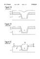
- FIG. 1Aillustrates the substrate 1, pad oxide layer 2, nitride polish stop layer 3, oxide liner 4 and insulating material 5. Planarization is implemented utilizing nitride layer 3 as a polish stop (FIG. 1B). The nitride layer 3 and pad oxide layer 2 are then stripped off (FIG. 1C), creating a step between the main surface 1a of substrate 1 and the uppermost surface 5a of the insulating material 5. The height of the step substantially corresponds to the combined thicknesses of the pad oxide layer R and the nitride polish stop layer S. The use of nitride polish stop layer 3 undesirably increases the height of the topographical step, adversely impacting planarity at the interface of substrate surface 1a and trench fill surface 5a.
- Such a topographical steprenders it difficult to photolithographically process subsequent layers of the device with accuracy, particularly in forming submicron features, thereby adversely affecting process yield and production cost. This problem becomes more acute as circuit geometry is continuously reduced to the 0.25 micron and under regime.
- the thickness S of the nitride layer 3typically about 1600 ⁇ to about 1800 ⁇ , cannot be reduced to the minimum necessary for it to function effectively as a polish stop (typically between about 300 ⁇ and about 1000 ⁇ depending on variables in the polishing process), because its thickness is optimized for photolithographic processing in defining the source/drain mask which, in turn, defines the trench areas.
- Accurate photolithographic processingrequires that the nitride layer 3 on which the mask is formed have a specific optical reflectivity which, in turn, requires the nitride layer 3 to have a thickness greater than that necessary for it to function as a polish stop.
- any change in the thickness of the nitride layer 3must be made in quantum increments; e.g., 400 ⁇ either thicker or thinner at a time, because of the nature of its optical properties. It is therefore difficult to optimize the thickness S of the nitride layer 3 as to its polish stop function without adversely impacting subsequent photolithographic processing.
- the disclosed methodologycomprises forming, on the pad oxide layer, a nitride layer whose thickness is optimized for its function as a polish stop (i.e., between about 300 ⁇ and about 1000 ⁇ ), then forming a reflectance compensation layer, such as silicon dioxide, on the nitride polish stop layer.
- the photoresist source/drain maskis formed on the reflectance compensation layer by a photolithographic process.
- the thickness of the reflectance compensation layeris such that the combined optical path length of the nitride polish stop layer and the reflectance compensation layer is about equal to the optical path length required by the photolithographic process, optical path length being the product of a material's index of refraction and its thickness.
- the trenchis thereafter etched and filled with an insulating material, then the insulating material and the reflectance compensation layer are planarized, as by CMP.
- An object of the present inventionis a method of manufacturing a semiconductor device having an insulated trench formed in a semiconductor substrate with improved flatness of the uppermost trench/substrate interface, thereby improving the accuracy of subsequent photolithographic processing.
- a method of manufacturing a semiconductor device having an insulated trench formed in a semiconductor substrate or in an epitaxial layer on the semiconductor substratecomprises: forming a pad oxide layer on a main surface of the substrate or epitaxial layer; forming a polish stop layer on the pad oxide layer, the polish stop layer comprising polysilicon or amorphous silicon and having a first thickness such that damage to the pad oxide layer does not occur during subsequent polishing, the polish stop layer having an upper surface and a first optical path length proportional to the first thickness; forming a reflectance compensation layer on the upper surface of the polish stop layer to a second thickness, the reflectance compensation layer having a second optical path length proportional to the second thickness; and forming a mask having an opening on the reflectance compensation layer by a photolithographic process; wherein the reflectance compensation and polish stop layers have a combined optical path length about equal to that required by the photolithographic process.
- Another aspect of the present inventionis a method of manufacturing an integrated circuit on a semiconductor substrate, comprising: forming a silicon dioxide pad layer on a main surface of the substrate or an epitaxial layer formed on the substrate; forming a polish stop layer on the silicon dioxide pad layer, the polish stop layer comprising amorphous silicon or polysilicon deposited by low pressure chemical vapor deposition (LPCVD) to a first thickness such that damage to the silicon dioxide pad layer does not occur during polishing, the polish stop layer having an upper surface and a first optical path length equal to the product of the first thickness and an index of refraction of the polish stop layer; forming a silicon dioxide reflectance compensation layer on the upper surface of the polish stop layer to a second thickness, the reflectance compensation layer having a second optical path length equal to the product of the second thickness and an index of refraction of the reflectance compensation layer, and comprising silicon dioxide derived from tetraethyl orthosilicate (TEOS) by LPCVD, silicon dioxide derived from silane by LPCVD,
- the insulating materialcomprising silicon dioxide derived from tetraethyl orthosilicate (TEOS) by LPCVD, silicon dioxide derived from silane by LPCVD, or a high density plasma oxide; and chemical-mechanical polishing such that an upper surface of the insulating material is substantially flush with the upper surface of the polish stop layer.
- TEOStetraethyl orthosilicate
- FIGS. 1A-1Cschematically illustrate sequential phases of a method of STI formation which results in a large topography between the insulating material and the main surface of the substrate.
- FIGS. 2A-2Hschematically illustrate sequential phases of a method in accordance with an embodiment of the present invention.
- the present inventionconstitutes an improvement over the methodology disclosed in copending application Ser. No. 08/993,859 (Attorney Docket No. 1033-294) by acheiving greater advantages by replacing the nitride polish stop with a material, such as amorphous silicon or polysilicon, which has superior polish stop properties to nitride, thereby enabling the inventive polish stop layer to be formed to a thickness less than the minimum thickness of a nitride polish stop layer, thus further reducing the height of topographical steps at the substrate/trench interface.
- Such topographical stepsseverely limit the capability of conventional photolithographic techniques in forming features with fine dimensions; e.g., less than about 0.25 ⁇ , particularly less than about 0.18 ⁇ .
- the present inventionenables the manufacture of semiconductor devices with a reduction in the height of such undesirable topographical steps at the substrate/trench interface.
- an amorphous silicon or polysilicon polish stop layer having a reduced thickness vis-a-vis conventional practicesis formed on a pad oxide layer which, in turn, is formed on a main surface of a semiconductor substrate or an epitaxial layer on a semiconductor substrate.
- substratedenotes a semiconductor substrate or an epitaxial layer formed on the semiconductor substrate.
- a reflectance compensation layersuch as silicon dioxide, is then deposited on the polish stop layer, and a photoresist source/drain mask is formed on the reflectance compensation layer.
- optical path lengthwhich denotes the thickness of a material at a given wavelength of light; i.e., how thick the layer on which the source/drain mask is formed appears at the wavelength at which the photolithographic process is conducted.
- Optical path lengthis the product of a material's refractive index and its thickness, and the optical path lengths of materials stacked on one another can be summed to obtain a total optical path length.
- the methodology of the present inventionutilizes the characteristics of optical path length to enable the thickness of the polish stop layer to be drastically reduced vis-a-vis conventional practices and vis-a-vis copending application Ser. No. 08/993,859 (Attorney Docket No. 1033-294), by providing the reflectance compensation layer on the polish stop layer and by providing a polish stop layer comprising a suitable material, e.g. amorphous silicon or polysilicon, which has superior polish stop properties.
- the reflectance compensation layerhas a thickness such that the sum of its optical path length and the optical path length of the polish stop layer is about equal to the optical path length required by the photolithographic process used to form the photoresist mask.
- the substrateis etched to form a trench, an oxide liner is grown in the trench surface, and the trench is filled with an insulating material.
- the insulating materialis then planarized, as by CMP, and the polish stop and pad oxide removed by etching, leaving a relatively small step between the insulating material and the main surface of the substrate.
- the provision of the reflectance compensation layerenables the thickness of the polish stop layer to be reduced to a minimum to function effectively as a polish stop, and the use of amorphous silicon or polysilicon as a polish stop enables the inventive polish stop layer to be thinner than previously employed nitride polish stop layers, due to the superior polish stop characteristics of amorphous silicon and polysilicon.
- the reduction of the thickness of the polish stopreduces topographical steps, thereby enabling substantial planarization of the insulating material.
- the reduction in topographical stepsenables application of subsequent layers with increased facility, and improves the accuracy of subsequent photolithographic processing, particularly with respect to minimal dimensions.
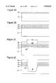
- FIGS. 2A-2HAn embodiment of the present invention is illustrated in FIGS. 2A-2H, wherein sequential phases in forming a semiconductor device in accordance with the present invention are depicted.
- substrate 21is prepared having a substantially planar surface, typically a semiconductor substrate comprising doped monocrystalline silicon or an epitaxial layer formed on a semiconductor substrate in accordance with conventional practices.
- a pad oxide layer 22is then grown on the substrate 21.
- Pad oxide layer 22typically comprises silicon oxide and can be thermally grown on the substrate or deposited by chemical vapor deposition (CVD) to a suitable thickness; e.g., about 100 ⁇ to about 200 ⁇ .
- CVDchemical vapor deposition
- a pad oxide containing a thinned thermally-grown silicon oxide layer and a buffer polycrystalline silicon layeris employed as the pad layer.
- Pad layer 22functions as a buffer layer cushioning stresses between substrate 21 and subsequently applied layers.
- FIG. 2Aillustrates silicon substrate 21 and the pad oxide layer 22.
- a polish stop layer 23is deposited on the pad oxide layer 22, as shown in FIG. 2B, such as an amorphous silicon layer by CVD or a polysilicon layer by CVD.
- a reflectance compensation layer 24is formed on the polish stop layer 23, such as a transparent silicon dioxide layer derived from tetraethyl orthosilicate (TEOS) by low pressure chemical vapor deposition (LPCVD), silicon dioxide derived from silane by LPCVD, or thermally grown silicon dioxide.
- TEOStetraethyl orthosilicate
- LPCVDlow pressure chemical vapor deposition
- reflectance compensation layer 24may comprise a translucent material which is absorptive at the exposure wavelength of the photolithography process, such as silicon oxynitride deposited by conventional methods, thus improving process control.
- the thickness of polish stop layer 23is chosen based on the required thickness for its function as a polish stop, depending on the variables of the polishing process. Additionally, the subsequent thermal growth of the oxide trench liner may cause partial consumption of the polish stop layer as oxygen diffuses through the reflectance compensation layer to react with the amorphous or polysilicon polish stop layer and form silicon dioxide. Thus, the thickness of the polish stop layer should be chosen such that after the liner oxidation step, the polish stop layer is at or above its minimum required thickness.
- the thickness of reflectance compensation layer 24is chosen based on the thickness of polish stop layer 23 and the reflectance requirements of the photolithography process subsequently employed to form the source/drain mask.
- photoresist mask 25is formed on reflectance compensation layer 24, as shown in FIG. 2C.
- Photoresist mask 25has a pattern defined by openings 250, which have a width 251 substantially corresponding to the width of the subsequently formed trench at the main surface 21a, such as about 0.25 ⁇ or less.
- the reflectance compensation layer 24 and polish stop layer 23are then removed by etching, and etching continued through the pad oxide layer 22 and into the substrate 21 to form the shallow trench 26, as shown in FIG. 2D.
- the trench 26is typically etched to a depth of up to about 4000 ⁇ ; e.g., about 2500 ⁇ to about 3000 ⁇ . After etching trench 26, photoresist 25 is stripped off the reflectance compensation layer 24.
- FIG. 2Eshows the trench 26 with the completed liner 27.
- trench 26is filled with a suitable insulating material 28, as shown in FIG. 2F.
- insulating materialcan comprise silicon dioxide derived from TEOS by LPCVD or derived from silane by LPCVD.
- the trench 26can also be filled with a high density plasma (HDP) oxide, preferably employing the methodology disclosed in copending application Ser. No. 08/924,133, filed Sep. 5, 1997, the entire disclosure of which is hereby incorporated herein by reference.
- HDPhigh density plasma
- planarizationis effected, as by CMP, such that an upper surface 28a of the insulating material 28 is substantially flush with an upper surface 23a of the polish stop 23, as shown in FIG. 2G.
- the polish stop layer 23 and the pad oxide layer 22are then stripped off, leaving the completed STI structure shown in FIG. 2H.
- the trench isolation structure formed in accordance with the present inventionenables formation of an STI structure using a thin amorphous silicon or polysilicon layer as a polish stop, thereby enabling the uppermost surface of the STI structure to be substantially coplanar with the main surface of the semiconductor substrate vis-a-vis conventional STI processes and vis-a-vis the process disclosed in copending application Ser. No. 08/993,859 (Attorney Docket No. 1033-294).
- the present inventionenables a reduction in the topography step between the insulating material and the main surface of the substrate, thereby significantly improving planarity. As a result, subsequent layers can be applied with greater facility and subsequent photolithographic processing performed with greater accuracy.
- the present inventionis applicable to the manufacture of various types of semiconductor devices having STI, particularly high density semiconductor devices having a design rule of about 0.25 ⁇ and under.
Landscapes
- Engineering & Computer Science (AREA)
- Physics & Mathematics (AREA)
- Condensed Matter Physics & Semiconductors (AREA)
- General Physics & Mathematics (AREA)
- Manufacturing & Machinery (AREA)
- Computer Hardware Design (AREA)
- Microelectronics & Electronic Packaging (AREA)
- Power Engineering (AREA)
- Element Separation (AREA)
Abstract
Description
The present invention relates to a method of manufacturing a semiconductor device comprising trench isolation. The invention has particular applicability in manufacturing high density semiconductor devices with submicron design features and active regions isolated by shallow insulated trenches.
Current demands for high density and performance associated with ultra large scale integration require submicron features of about 0.25 microns and under, increased transistor and circuit speeds and improved reliability. Such demands for increased density, performance and reliability require formation of device features with high precision and uniformity.
Conventional semiconductor devices comprise a substrate and various electrically isolated regions, called active regions, in which individual circuit components are formed. The electrical isolation of these active regions is typically accomplished by thermal oxidation of the semiconductor substrate, typically monocrystalline silicon or an epitaxial layer formed thereon, bounding the active regions.
One type of isolation structure is known as trench isolation, wherein shallow trenches are etched in the substrate and an oxide liner is thermally grown on the trench walls. The trench is then refilled with an insulating material. The resulting structure is referred to as a shallow trench isolation (STI) structure. The active region typically comprises source/drain regions formed in the semiconductor substrate by implantation of impurities, spaced apart by a channel region on which a gate electrode is formed with a gate oxide layer therebetween. The gate electrode controls the turn-on and turn-off of each transistor.
A typical method of trench formation comprises initially growing a pad oxide layer on the substrate, and depositing a nitride polish stop layer thereon. A photoresist mask is then applied to define the trench areas. The exposed portions of the nitride layer are then etched away, followed by the pad oxide layer. The etching continues into the substrate to form the shallow trench. When etching of the trench is completed, the photoresist is stripped off the nitride layer.
Next, the substrate is oxidized to form an oxide liner on the walls and base of the trench to control the silicon-silicon dioxide interface quality. The trench is then refilled with an insulating material (or "trench fill"), such as silicon dioxide derived from tetraethyl orthosilicate (TEOS). The surface is then planarized, as by chemical-mechanical polishing (CMP) using the nitride layer as a polish stop, and the nitride and pad oxide are stripped off the active areas to complete the trench isolation structure.
When creating the STI structure, it is considered ideal for the uppermost surface of the substrate to be flush (i.e., coplanar) with the uppermost surface of the trench fill, in order to provide a flat topography for subsequent processing, particularly photolithographic processing, thereby facilitating accurate formation of submicron features, particularly features of about 0.25 microns and under. However, substantial planarity is difficult to achieve. For example, the use of a nitride layer as a polish stop results in the undesirable formation of a step.
FIG. 1A illustrates the substrate 1, pad oxide layer 2, nitridepolish stop layer 3,oxide liner 4 andinsulating material 5. Planarization is implemented utilizingnitride layer 3 as a polish stop (FIG. 1B). Thenitride layer 3 and pad oxide layer 2 are then stripped off (FIG. 1C), creating a step between themain surface 1a of substrate 1 and theuppermost surface 5a of theinsulating material 5. The height of the step substantially corresponds to the combined thicknesses of the pad oxide layer R and the nitride polish stop layer S. The use of nitridepolish stop layer 3 undesirably increases the height of the topographical step, adversely impacting planarity at the interface ofsubstrate surface 1a andtrench fill surface 5a. Such a topographical step renders it difficult to photolithographically process subsequent layers of the device with accuracy, particularly in forming submicron features, thereby adversely affecting process yield and production cost. This problem becomes more acute as circuit geometry is continuously reduced to the 0.25 micron and under regime.
Unfortunately, the thickness S of thenitride layer 3, typically about 1600 Å to about 1800 Å, cannot be reduced to the minimum necessary for it to function effectively as a polish stop (typically between about 300 Å and about 1000 Å depending on variables in the polishing process), because its thickness is optimized for photolithographic processing in defining the source/drain mask which, in turn, defines the trench areas. Accurate photolithographic processing requires that thenitride layer 3 on which the mask is formed have a specific optical reflectivity which, in turn, requires thenitride layer 3 to have a thickness greater than that necessary for it to function as a polish stop. Furthermore, any change in the thickness of thenitride layer 3 must be made in quantum increments; e.g., 400 Å either thicker or thinner at a time, because of the nature of its optical properties. It is therefore difficult to optimize the thickness S of thenitride layer 3 as to its polish stop function without adversely impacting subsequent photolithographic processing.
In copending application Ser. No. 08/993,859, filed Dec. 18, 1997 (Attorney Docket No. 1033-294), a method is disclosed for forming trench isolation wherein the thickness of the nitride polish stop layer is reduced vis-a-vis conventional practices, thereby reducing the topological step between the main surface of the semiconductor substrate and the uppermost surface of the trench fill. The disclosed methodology comprises forming, on the pad oxide layer, a nitride layer whose thickness is optimized for its function as a polish stop (i.e., between about 300 Å and about 1000 Å), then forming a reflectance compensation layer, such as silicon dioxide, on the nitride polish stop layer. The photoresist source/drain mask is formed on the reflectance compensation layer by a photolithographic process. The thickness of the reflectance compensation layer is such that the combined optical path length of the nitride polish stop layer and the reflectance compensation layer is about equal to the optical path length required by the photolithographic process, optical path length being the product of a material's index of refraction and its thickness. The trench is thereafter etched and filled with an insulating material, then the insulating material and the reflectance compensation layer are planarized, as by CMP.
With the provision of a reflectance compensation layer, the methodology disclosed in copending application Ser. No. 08/993,859 (Attorney Docket No. 1033-294) reduces the thickness of the nitride polish stop layer compared to conventional practices, thereby reducing the height of undesirable topological steps at the substrate/trench interface. However, this methodology is limited to reducing the step height only to the minimum thickness required for the nitride polish stop to perform its function; i.e., about 300 Å.
There exists a continuing need for a method of manufacturing a semiconductor device which enables further reduction in the topographical step between the uppermost surface of the substrate or epitaxial layer and the uppermost surface of the trench, without adversely affecting photolithographic processing of the source/drain mask.
An object of the present invention is a method of manufacturing a semiconductor device having an insulated trench formed in a semiconductor substrate with improved flatness of the uppermost trench/substrate interface, thereby improving the accuracy of subsequent photolithographic processing.
Additional objects, advantages and other features of the invention will be set forth in part in the description which follows and in part will become apparent to those having ordinary skill in the art upon examination of the following or may be learned from the practice of the invention. The objects and advantages of the invention may be realized and obtained as particularly pointed out in the appended claims.
According to the present invention, the foregoing and other objects are achieved in part by a method of manufacturing a semiconductor device having an insulated trench formed in a semiconductor substrate or in an epitaxial layer on the semiconductor substrate, which method comprises: forming a pad oxide layer on a main surface of the substrate or epitaxial layer; forming a polish stop layer on the pad oxide layer, the polish stop layer comprising polysilicon or amorphous silicon and having a first thickness such that damage to the pad oxide layer does not occur during subsequent polishing, the polish stop layer having an upper surface and a first optical path length proportional to the first thickness; forming a reflectance compensation layer on the upper surface of the polish stop layer to a second thickness, the reflectance compensation layer having a second optical path length proportional to the second thickness; and forming a mask having an opening on the reflectance compensation layer by a photolithographic process; wherein the reflectance compensation and polish stop layers have a combined optical path length about equal to that required by the photolithographic process.
Another aspect of the present invention is a method of manufacturing an integrated circuit on a semiconductor substrate, comprising: forming a silicon dioxide pad layer on a main surface of the substrate or an epitaxial layer formed on the substrate; forming a polish stop layer on the silicon dioxide pad layer, the polish stop layer comprising amorphous silicon or polysilicon deposited by low pressure chemical vapor deposition (LPCVD) to a first thickness such that damage to the silicon dioxide pad layer does not occur during polishing, the polish stop layer having an upper surface and a first optical path length equal to the product of the first thickness and an index of refraction of the polish stop layer; forming a silicon dioxide reflectance compensation layer on the upper surface of the polish stop layer to a second thickness, the reflectance compensation layer having a second optical path length equal to the product of the second thickness and an index of refraction of the reflectance compensation layer, and comprising silicon dioxide derived from tetraethyl orthosilicate (TEOS) by LPCVD, silicon dioxide derived from silane by LPCVD, silicon dioxide thermally grown, or silicon oxynitride; forming a photoresist mask having an opening on the reflectance compensation layer by a photolithographic process, wherein the reflectance compensation layer and polish stop layer have a combined optical path length about equal to that required by the photolithographic process; etching to remove portions of the underlying reflectance compensation layer, polish stop layer and silicon dioxide pad layer and to form a trench in the substrate or epitaxial layer at a depth of up to about 4000 Å; removing the mask; thermally growing a thin silicon oxide liner on an internal surface of the trench and in contact with the silicon dioxide pad layer by heating to a temperature of at least about 1000° C. depositing an insulating material filling the trench, the insulating material comprising silicon dioxide derived from tetraethyl orthosilicate (TEOS) by LPCVD, silicon dioxide derived from silane by LPCVD, or a high density plasma oxide; and chemical-mechanical polishing such that an upper surface of the insulating material is substantially flush with the upper surface of the polish stop layer.
Additional objects and advantages of the present invention will become readily apparent to those skilled in this art from the following detailed description, wherein only the preferred embodiment of the invention is shown and described, simply by way of illustration of the best mode contemplated for carrying out the invention. As will be realized, the invention is capable of other and different embodiments, and its several details are capable of modifications in various obvious respects, all without departing from the invention. Accordingly, the drawings and description are to be regarded as illustrative in nature, and not as restrictive.
Reference is made to the attached drawings, wherein elements having the same reference numeral designations represent like elements throughout, and wherein:
FIGS. 1A-1C schematically illustrate sequential phases of a method of STI formation which results in a large topography between the insulating material and the main surface of the substrate.
FIGS. 2A-2H schematically illustrate sequential phases of a method in accordance with an embodiment of the present invention.
The present invention constitutes an improvement over the methodology disclosed in copending application Ser. No. 08/993,859 (Attorney Docket No. 1033-294) by acheiving greater advantages by replacing the nitride polish stop with a material, such as amorphous silicon or polysilicon, which has superior polish stop properties to nitride, thereby enabling the inventive polish stop layer to be formed to a thickness less than the minimum thickness of a nitride polish stop layer, thus further reducing the height of topographical steps at the substrate/trench interface. Such topographical steps severely limit the capability of conventional photolithographic techniques in forming features with fine dimensions; e.g., less than about 0.25μ, particularly less than about 0.18μ. The present invention enables the manufacture of semiconductor devices with a reduction in the height of such undesirable topographical steps at the substrate/trench interface.
According to the methodology of the present invention, an amorphous silicon or polysilicon polish stop layer having a reduced thickness vis-a-vis conventional practices is formed on a pad oxide layer which, in turn, is formed on a main surface of a semiconductor substrate or an epitaxial layer on a semiconductor substrate. As used throughout the present disclosure and claims, the term "substrate" denotes a semiconductor substrate or an epitaxial layer formed on the semiconductor substrate. A reflectance compensation layer, such as silicon dioxide, is then deposited on the polish stop layer, and a photoresist source/drain mask is formed on the reflectance compensation layer.
The photolithographic process employed to create the source/drain mask typically requires the layer on which the mask is formed to exhibit certain optical properties, one of the most important being reflectance. A key parameter determining reflectance is optical path length, which denotes the thickness of a material at a given wavelength of light; i.e., how thick the layer on which the source/drain mask is formed appears at the wavelength at which the photolithographic process is conducted. Optical path length is the product of a material's refractive index and its thickness, and the optical path lengths of materials stacked on one another can be summed to obtain a total optical path length. The methodology of the present invention utilizes the characteristics of optical path length to enable the thickness of the polish stop layer to be drastically reduced vis-a-vis conventional practices and vis-a-vis copending application Ser. No. 08/993,859 (Attorney Docket No. 1033-294), by providing the reflectance compensation layer on the polish stop layer and by providing a polish stop layer comprising a suitable material, e.g. amorphous silicon or polysilicon, which has superior polish stop properties. The reflectance compensation layer has a thickness such that the sum of its optical path length and the optical path length of the polish stop layer is about equal to the optical path length required by the photolithographic process used to form the photoresist mask.
After masking, the substrate is etched to form a trench, an oxide liner is grown in the trench surface, and the trench is filled with an insulating material. The insulating material is then planarized, as by CMP, and the polish stop and pad oxide removed by etching, leaving a relatively small step between the insulating material and the main surface of the substrate.
The provision of the reflectance compensation layer enables the thickness of the polish stop layer to be reduced to a minimum to function effectively as a polish stop, and the use of amorphous silicon or polysilicon as a polish stop enables the inventive polish stop layer to be thinner than previously employed nitride polish stop layers, due to the superior polish stop characteristics of amorphous silicon and polysilicon. The reduction of the thickness of the polish stop reduces topographical steps, thereby enabling substantial planarization of the insulating material. The reduction in topographical steps enables application of subsequent layers with increased facility, and improves the accuracy of subsequent photolithographic processing, particularly with respect to minimal dimensions.
An embodiment of the present invention is illustrated in FIGS. 2A-2H, wherein sequential phases in forming a semiconductor device in accordance with the present invention are depicted. Referring to FIG. 2A,substrate 21 is prepared having a substantially planar surface, typically a semiconductor substrate comprising doped monocrystalline silicon or an epitaxial layer formed on a semiconductor substrate in accordance with conventional practices. Apad oxide layer 22 is then grown on thesubstrate 21.Pad oxide layer 22 typically comprises silicon oxide and can be thermally grown on the substrate or deposited by chemical vapor deposition (CVD) to a suitable thickness; e.g., about 100 Å to about 200 Å. In another embodiment, a pad oxide containing a thinned thermally-grown silicon oxide layer and a buffer polycrystalline silicon layer is employed as the pad layer.Pad layer 22 functions as a buffer layer cushioning stresses betweensubstrate 21 and subsequently applied layers. FIG. 2A illustratessilicon substrate 21 and thepad oxide layer 22.
After formation of thepad oxide layer 22, apolish stop layer 23 is deposited on thepad oxide layer 22, as shown in FIG. 2B, such as an amorphous silicon layer by CVD or a polysilicon layer by CVD. Areflectance compensation layer 24 is formed on thepolish stop layer 23, such as a transparent silicon dioxide layer derived from tetraethyl orthosilicate (TEOS) by low pressure chemical vapor deposition (LPCVD), silicon dioxide derived from silane by LPCVD, or thermally grown silicon dioxide. Alternatively,reflectance compensation layer 24 may comprise a translucent material which is absorptive at the exposure wavelength of the photolithography process, such as silicon oxynitride deposited by conventional methods, thus improving process control.
The thickness ofpolish stop layer 23 is chosen based on the required thickness for its function as a polish stop, depending on the variables of the polishing process. Additionally, the subsequent thermal growth of the oxide trench liner may cause partial consumption of the polish stop layer as oxygen diffuses through the reflectance compensation layer to react with the amorphous or polysilicon polish stop layer and form silicon dioxide. Thus, the thickness of the polish stop layer should be chosen such that after the liner oxidation step, the polish stop layer is at or above its minimum required thickness. The thickness ofreflectance compensation layer 24 is chosen based on the thickness ofpolish stop layer 23 and the reflectance requirements of the photolithography process subsequently employed to form the source/drain mask.
After formation of thereflectance compensation layer 24,photoresist mask 25 is formed onreflectance compensation layer 24, as shown in FIG. 2C.Photoresist mask 25 has a pattern defined byopenings 250, which have awidth 251 substantially corresponding to the width of the subsequently formed trench at themain surface 21a, such as about 0.25μ or less. Thereflectance compensation layer 24 andpolish stop layer 23 are then removed by etching, and etching continued through thepad oxide layer 22 and into thesubstrate 21 to form theshallow trench 26, as shown in FIG. 2D. Thetrench 26 is typically etched to a depth of up to about 4000 Å; e.g., about 2500 Å to about 3000 Å. After etchingtrench 26,photoresist 25 is stripped off thereflectance compensation layer 24.
Thereafter, the trench surface is thermally oxidized to form anoxide liner 27 on the inner surface oftrench 26 and in contact with thepad oxide layer 22, typically at a temperature of at least about 1000° C. FIG. 2E shows thetrench 26 with the completedliner 27. Subsequent to formation of theoxide liner 27,trench 26 is filled with a suitable insulatingmaterial 28, as shown in FIG. 2F. Such insulating material can comprise silicon dioxide derived from TEOS by LPCVD or derived from silane by LPCVD. Thetrench 26 can also be filled with a high density plasma (HDP) oxide, preferably employing the methodology disclosed in copending application Ser. No. 08/924,133, filed Sep. 5, 1997, the entire disclosure of which is hereby incorporated herein by reference. Subsequent to trench filling, planarization is effected, as by CMP, such that anupper surface 28a of the insulatingmaterial 28 is substantially flush with anupper surface 23a of thepolish stop 23, as shown in FIG. 2G. Thepolish stop layer 23 and thepad oxide layer 22 are then stripped off, leaving the completed STI structure shown in FIG. 2H.
The trench isolation structure formed in accordance with the present invention enables formation of an STI structure using a thin amorphous silicon or polysilicon layer as a polish stop, thereby enabling the uppermost surface of the STI structure to be substantially coplanar with the main surface of the semiconductor substrate vis-a-vis conventional STI processes and vis-a-vis the process disclosed in copending application Ser. No. 08/993,859 (Attorney Docket No. 1033-294). The present invention enables a reduction in the topography step between the insulating material and the main surface of the substrate, thereby significantly improving planarity. As a result, subsequent layers can be applied with greater facility and subsequent photolithographic processing performed with greater accuracy. The present invention is applicable to the manufacture of various types of semiconductor devices having STI, particularly high density semiconductor devices having a design rule of about 0.25μ and under.
The present invention can be practiced by employing conventional materials, methodology and equipment. Accordingly, the details of such materials, equipment and methodology are not set forth herein in detail. In the previous descriptions, numerous specific details are set forth, such as specific materials, structures, chemicals, processes, etc., in order to provide a thorough understanding of the present invention. However, as one having ordinary skill in the art would recognize, the present invention can be practiced without resorting to the details specifically set forth. In other instances, well known processing structures have not been described in detail, in order not to unnecessarily obscure the present invention.
Only the preferred embodiment of the invention and but a few examples of its versatility are shown and described in the present disclosure. It is to be understood that the invention is capable of use in various other combinations and environments and is capable of changes or modifications within the scope of the inventive concept as expressed herein.
Claims (17)
1. A method of manufacturing a semiconductor device having an insulated trench formed in a semiconductor substrate or in an epitaxial layer on the semiconductor substrate, which method comprises:
forming a pad oxide layer on a main surface of the substrate or epitaxial layer;
forming a polish stop layer on the pad oxide layer, the polish stop layer comprising polysilicon or amorphous silicon and having a first thickness, an upper surface and a first optical path length proportional to the first thickness;
forming a reflectance compensation layer on the upper surface of the polish stop layer to a second thickness, the reflectance compensation layer having a second optical path length proportional to the second thickness; and
forming a mask having an opening on the reflectance compensation layer by a photolithographic process;
wherein the first thickness is about the minimum thickness such that damage to the pad oxide layer does not occur during subsequent polishing; and
wherein the reflectance compensation and polish stop layers have a combined optical path length about equal to that required by the photolithographic process.
2. The method according to claim 1, wherein the pad oxide layer comprises silicon dioxide having a thickness of about 100 Å to about 200 Å.
3. The method according to claim 1, wherein the reflectance compensation layer comprises silicon dioxide derived from tetraethyl orthosilicate (TEOS) by low pressure chemical vapor deposition (LPCVD), silicon dioxide derived from silane by LPCVD, silicon dioxide thermally grown, or silicon oxynitride.
4. The method according to claim 1, wherein the mask comprises a photoresist mask.
5. The method according to claim 1, wherein the first optical path length is equal to the product of the first thickness and an index of refraction of the polish stop layer, and the second optical path length is equal to the product of the second thickness and an index of refraction of the reflectance compensation layer.
6. The method according to claim 1, wherein the polish stop layer is deposited by low pressure chemical vapor deposition.
7. The method according to claim 1, which method further comprises:
etching to remove portions of the underlying reflectance compensation layer, polish stop layer and pad oxide layer and to form the trench in the substrate or epitaxial layer;
removing the mask;
depositing an insulating material filling the trench;
planarizing such that an upper surface of the insulating material is substantially flush with the upper surface of the polish stop layer; and
etching to remove the polish stop layer and pad oxide layer.
8. The method according to claim 7, comprising, prior to depositing the insulating material, heating at a temperature of at least about 1000° C. to thermally grow a silicon oxide liner on an internal surface of the trench and in contact with the pad oxide layer.
9. The method according to claim 7, wherein the insulating material comprises silicon dioxide derived from tetraethyl orthosilicate (TEOS) by low pressure chemical vapor deposition (LPCVD), silicon dioxide derived from silane by LPCVD, or a high density plasma oxide.
10. The method according to claim 7, wherein the opening in the mask has a width substantially equal to a width of the trench at the main surface.
11. The method according to claim 9, comprising polishing by chemical-mechanical polishing.
12. The method according to claim 10, wherein the width of the opening is about 0.25μ or under.
13. The method according to claim 12, wherein the trench is etched to a depth of up to about 4000 Å.
14. The method according to claim 13, wherein the trench is etched to a depth of about 2500 Å to about 3000 Å.
15. A method of manufacturing an integrated circuit on a semiconductor substrate, comprising:
forming a silicon dioxide pad layer on a main surface of the substrate or an epitaxial layer formed on the substrate;
forming a polish stop layer on the silicon dioxide pad layer, the polish stop layer comprising amorphous silicon or polysilicon deposited by low pressure chemical vapor deposition (LPCVD) to a first thickness such that damage to the silicon dioxide pad layer does not occur during polishing, the polish stop layer having an upper surface and a first optical path length equal to the product of the first thickness and an index of refraction of the polish stop layer;
forming a silicon dioxide reflectance compensation layer on the upper surface of the polish stop layer to a second thickness, the reflectance compensation layer having a second optical path length equal to the product of the second thickness and an index of refraction of the reflectance compensation layer, and comprising silicon dioxide derived from tetraethyl orthosilicate (TEOS) by LPCVD, silicon dioxide derived from silane by LPCVD, silicon dioxide thermally grown, or silicon oxynitride;
forming a photoresist mask having an opening on the reflectance compensation layer by a photolithographic process, wherein the reflectance compensation layer and polish stop layer have a combined optical path length about equal to that required by the photolithographic process;
etching to remove portions of the underlying reflectance compensation layer, polish stop layer and silicon dioxide pad layer and to form a trench in the substrate or epitaxial layer at a depth of up to about 4000 Å;
removing the mask;
thermally growing a thin silicon oxide liner on an internal surface of the trench and in contact with the silicon dioxide pad layer by heating to a temperature of at least about 1000° C.;
depositing an insulating material filling the trench, the insulating material comprising silicon dioxide derived from tetraethyl orthosilicate (TEOS) by LPCVD, silicon dioxide derived from silane by LPCVD, or a high density plasma oxide; and
chemical-mechanical polishing such that an upper surface of the insulating material is substantially flush with the upper surface of the polish stop layer.
16. A method of manufacturing a semiconductor device having an insulated trench formed in a semiconductor substrate or in an epitaxial layer on the semiconductor substrate, which method comprises:
forming a pad oxide layer on a main surface of the substrate or epitaxial layer;
forming a polish stop layer on the pad oxide layer, the polish stop layer comprising a layer of a material having a greater resistance to chemical mechanical polishing than silicon nitride, having a first thickness such that damage to the pad oxide layer does not occur during subsequent chemical mechanical polishing, an upper surface, and a first optical path length proportional to the first thickness;
forming a reflectance compensation layer on the upper surface of the polish stop layer to a second thickness, the reflectance compensation layer having a second optical path length proportional to the second thickness; and
forming a mask having an opening on the reflectance compensation layer by a photolithographic process;
wherein the reflectance compensation and polish stop layers have a combined optical path length about equal to that required by the photolithographic process.
17. The method according to claim 16, which method further comprises:
etching to remove portions of the underlying reflectance compensation layer, polish stop layer and pad oxide layer and to form the trench in the substrate or epitaxial layer;
removing the mask;
depositing an insulating material filling the trench;
planarizing such that an upper surface of the insulating material is substantially flush with the upper surface of the polish stop layer; and
etching to remove the polish stop layer and pad oxide layer.
Priority Applications (1)
| Application Number | Priority Date | Filing Date | Title |
|---|---|---|---|
| US08/993,881US5930645A (en) | 1997-12-18 | 1997-12-18 | Shallow trench isolation formation with reduced polish stop thickness |
Applications Claiming Priority (1)
| Application Number | Priority Date | Filing Date | Title |
|---|---|---|---|
| US08/993,881US5930645A (en) | 1997-12-18 | 1997-12-18 | Shallow trench isolation formation with reduced polish stop thickness |
Publications (1)
| Publication Number | Publication Date |
|---|---|
| US5930645Atrue US5930645A (en) | 1999-07-27 |
Family
ID=25540033
Family Applications (1)
| Application Number | Title | Priority Date | Filing Date |
|---|---|---|---|
| US08/993,881Expired - LifetimeUS5930645A (en) | 1997-12-18 | 1997-12-18 | Shallow trench isolation formation with reduced polish stop thickness |
Country Status (1)
| Country | Link |
|---|---|
| US (1) | US5930645A (en) |
Cited By (36)
| Publication number | Priority date | Publication date | Assignee | Title |
|---|---|---|---|---|
| US5998278A (en)* | 1998-02-13 | 1999-12-07 | United Integrated Circuits Corp. | Method of fabricating shallow trench isolation structures using a oxidized polysilicon trench mask |
| US6063689A (en)* | 1998-07-06 | 2000-05-16 | United Microelectronics Corp. | Method for forming an isolation |
| US6074927A (en)* | 1998-06-01 | 2000-06-13 | Advanced Micro Devices, Inc. | Shallow trench isolation formation with trench wall spacer |
| US6090713A (en)* | 1997-12-18 | 2000-07-18 | Advanced Micro Devices, Inc. | Shallow trench isolation formation with simplified reverse planarization mask |
| US6100161A (en)* | 1999-11-18 | 2000-08-08 | Chartered Semiconductor Manufacturing Ltd. | Method of fabrication of a raised source/drain transistor |
| US6159821A (en)* | 1999-02-12 | 2000-12-12 | Vanguard International Semiconductor Corporation | Methods for shallow trench isolation |
| US6180490B1 (en)* | 1999-05-25 | 2001-01-30 | Chartered Semiconductor Manufacturing Ltd. | Method of filling shallow trenches |
| WO2001031701A1 (en)* | 1999-10-28 | 2001-05-03 | Koninklijke Philips Electronics N.V. | Method for suppressing narrow width effects in cmos technology |
| US6277710B1 (en)* | 1999-11-15 | 2001-08-21 | Chartered Semiconductor Manufacturing Ltd. | Method of forming shallow trench isolation |
| US6300219B1 (en)* | 1999-08-30 | 2001-10-09 | Micron Technology, Inc. | Method of forming trench isolation regions |
| US6403492B1 (en) | 2001-02-02 | 2002-06-11 | Advanced Micro Devices, Inc. | Method of manufacturing semiconductor devices with trench isolation |
| US6409936B1 (en)* | 1999-02-16 | 2002-06-25 | Micron Technology, Inc. | Composition and method of formation and use therefor in chemical-mechanical polishing |
| US20020086543A1 (en)* | 2001-01-03 | 2002-07-04 | Trapp Shane J. | Method of forming integrated circuitry and method of forming shallow trench isolation in a semiconductor substrate |
| US6426295B1 (en)* | 1999-02-16 | 2002-07-30 | Micron Technology, Inc. | Reduction of surface roughness during chemical mechanical planarization(CMP) |
| US6482715B2 (en)* | 2000-12-16 | 2002-11-19 | Samsung Electronics Co., Ltd. | Method of forming shallow trench isolation layer in semiconductor device |
| US6500728B1 (en) | 2002-05-24 | 2002-12-31 | Taiwan Semiconductor Manufacturing Company | Shallow trench isolation (STI) module to improve contact etch process window |
| US6559028B1 (en)* | 2002-01-18 | 2003-05-06 | Advanced Micro Devices, Inc. | Method of topography management in semiconductor formation |
| US6566225B2 (en)* | 2001-08-06 | 2003-05-20 | Macronix International Co., Ltd. | Formation method of shallow trench isolation |
| US6638866B1 (en) | 2001-10-18 | 2003-10-28 | Taiwan Semiconductor Manufacturing Company | Chemical-mechanical polishing (CMP) process for shallow trench isolation |
| US6805614B2 (en)* | 2000-11-30 | 2004-10-19 | Texas Instruments Incorporated | Multilayered CMP stop for flat planarization |
| US6815353B2 (en)* | 2002-02-05 | 2004-11-09 | Micrel, Incorporated | Multi-layer film stack polish stop |
| US20050009368A1 (en)* | 2003-07-07 | 2005-01-13 | Vaartstra Brian A. | Methods of forming a phosphorus doped silicon dioxide comprising layer, and methods of forming trench isolation in the fabrication of integrated circuitry |
| US20050054213A1 (en)* | 2003-09-05 | 2005-03-10 | Derderian Garo J. | Methods of depositing a silicon dioxide comprising layer in the fabrication of integrated circuitry, and methods of forming trench isolation in the fabrication of integrated circuitry |
| US20050098380A1 (en)* | 2003-09-23 | 2005-05-12 | Luscombe Terry L. | Vehicle mounted utility apparatus with quick attachment means |
| US20050208778A1 (en)* | 2004-03-22 | 2005-09-22 | Weimin Li | Methods of depositing silicon dioxide comprising layers in the fabrication of integrated circuitry, methods of forming trench isolation, and methods of forming arrays of memory cells |
| US20060046425A1 (en)* | 2004-08-31 | 2006-03-02 | Sandhu Gurtej S | Methods of forming trench isolation in the fabrication of integrated circuitry, methods of fabricating memory circuitry, integrated circuitry and memory integrated circuitry |
| US7056804B1 (en)* | 2004-03-01 | 2006-06-06 | Advanced Micro Devices, Inc. | Shallow trench isolation polish stop layer for reduced topography |
| US20060183294A1 (en)* | 2005-02-17 | 2006-08-17 | Micron Technology, Inc. | Methods of forming integrated circuitry |
| US20060197225A1 (en)* | 2005-03-07 | 2006-09-07 | Qi Pan | Electrically conductive line, method of forming an electrically conductive line, and method of reducing titanium silicide agglomeration in fabrication of titanium silicide over polysilicon transistor gate lines |
| US20060223279A1 (en)* | 2005-04-01 | 2006-10-05 | Micron Technology, Inc. | Methods of forming trench isolation in the fabrication of integrated circuitry and methods of fabricating integrated circuitry |
| US20070155178A1 (en)* | 2000-05-22 | 2007-07-05 | Samsung Electronics Co., Ltd. | Slurry for chemical mechanical polishing process and method of manufacturing semiconductor device using the same |
| US20070264794A1 (en)* | 2006-05-11 | 2007-11-15 | Micron Technology, Inc. | Methods of forming trench isolation and methods of forming arrays of FLASH memory cells |
| US20070264777A1 (en)* | 2006-05-15 | 2007-11-15 | Micron Technology, Inc. | Method for forming a floating gate using chemical mechanical planarization |
| US20080230830A1 (en)* | 2007-03-22 | 2008-09-25 | Hynix Semiconductor Inc. | Nonvolatile memory device and method of fabricating the same |
| US20080280442A1 (en)* | 2007-05-09 | 2008-11-13 | Hynix Semiconductor Inc. | Method for fabricating semiconductor device |
| US20110092061A1 (en)* | 2009-10-20 | 2011-04-21 | Yunjun Ho | Methods of Forming Silicon Oxides and Methods of Forming Interlevel Dielectrics |
Citations (12)
| Publication number | Priority date | Publication date | Assignee | Title |
|---|---|---|---|---|
| US3721584A (en)* | 1970-04-13 | 1973-03-20 | A Diem | Silicon coated substrates and objects fabricated therefrom |
| US4697089A (en)* | 1986-06-18 | 1987-09-29 | Tegal Corporation | Dual wavelength sensor which employs object as part of a corner reflector |
| US5217920A (en)* | 1992-06-18 | 1993-06-08 | Motorola, Inc. | Method of forming substrate contact trenches and isolation trenches using anodization for isolation |
| US5229316A (en)* | 1992-04-16 | 1993-07-20 | Micron Technology, Inc. | Semiconductor processing method for forming substrate isolation trenches |
| US5455194A (en)* | 1995-03-06 | 1995-10-03 | Motorola Inc. | Encapsulation method for localized oxidation of silicon with trench isolation |
| US5506168A (en)* | 1992-10-27 | 1996-04-09 | Kabushiki Kaisha Toshiba | Method for manufacturing semiconductor device |
| US5536675A (en)* | 1993-12-30 | 1996-07-16 | Intel Corporation | Isolation structure formation for semiconductor circuit fabrication |
| US5578518A (en)* | 1993-12-20 | 1996-11-26 | Kabushiki Kaisha Toshiba | Method of manufacturing a trench isolation having round corners |
| US5712185A (en)* | 1996-04-23 | 1998-01-27 | United Microelectronics | Method for forming shallow trench isolation |
| US5721172A (en)* | 1996-12-02 | 1998-02-24 | Taiwan Semiconductor Manufacturing Company, Ltd. | Self-aligned polish stop layer hard masking method for forming planarized aperture fill layers |
| US5763315A (en)* | 1997-01-28 | 1998-06-09 | International Business Machines Corporation | Shallow trench isolation with oxide-nitride/oxynitride liner |
| US5776808A (en)* | 1996-12-26 | 1998-07-07 | Siemens Aktiengesellschaft | Pad stack with a poly SI etch stop for TEOS mask removal with RIE |
- 1997
- 1997-12-18USUS08/993,881patent/US5930645A/ennot_activeExpired - Lifetime
Patent Citations (12)
| Publication number | Priority date | Publication date | Assignee | Title |
|---|---|---|---|---|
| US3721584A (en)* | 1970-04-13 | 1973-03-20 | A Diem | Silicon coated substrates and objects fabricated therefrom |
| US4697089A (en)* | 1986-06-18 | 1987-09-29 | Tegal Corporation | Dual wavelength sensor which employs object as part of a corner reflector |
| US5229316A (en)* | 1992-04-16 | 1993-07-20 | Micron Technology, Inc. | Semiconductor processing method for forming substrate isolation trenches |
| US5217920A (en)* | 1992-06-18 | 1993-06-08 | Motorola, Inc. | Method of forming substrate contact trenches and isolation trenches using anodization for isolation |
| US5506168A (en)* | 1992-10-27 | 1996-04-09 | Kabushiki Kaisha Toshiba | Method for manufacturing semiconductor device |
| US5578518A (en)* | 1993-12-20 | 1996-11-26 | Kabushiki Kaisha Toshiba | Method of manufacturing a trench isolation having round corners |
| US5536675A (en)* | 1993-12-30 | 1996-07-16 | Intel Corporation | Isolation structure formation for semiconductor circuit fabrication |
| US5455194A (en)* | 1995-03-06 | 1995-10-03 | Motorola Inc. | Encapsulation method for localized oxidation of silicon with trench isolation |
| US5712185A (en)* | 1996-04-23 | 1998-01-27 | United Microelectronics | Method for forming shallow trench isolation |
| US5721172A (en)* | 1996-12-02 | 1998-02-24 | Taiwan Semiconductor Manufacturing Company, Ltd. | Self-aligned polish stop layer hard masking method for forming planarized aperture fill layers |
| US5776808A (en)* | 1996-12-26 | 1998-07-07 | Siemens Aktiengesellschaft | Pad stack with a poly SI etch stop for TEOS mask removal with RIE |
| US5763315A (en)* | 1997-01-28 | 1998-06-09 | International Business Machines Corporation | Shallow trench isolation with oxide-nitride/oxynitride liner |
Cited By (87)
| Publication number | Priority date | Publication date | Assignee | Title |
|---|---|---|---|---|
| US6090713A (en)* | 1997-12-18 | 2000-07-18 | Advanced Micro Devices, Inc. | Shallow trench isolation formation with simplified reverse planarization mask |
| US5998278A (en)* | 1998-02-13 | 1999-12-07 | United Integrated Circuits Corp. | Method of fabricating shallow trench isolation structures using a oxidized polysilicon trench mask |
| US6074927A (en)* | 1998-06-01 | 2000-06-13 | Advanced Micro Devices, Inc. | Shallow trench isolation formation with trench wall spacer |
| US6063689A (en)* | 1998-07-06 | 2000-05-16 | United Microelectronics Corp. | Method for forming an isolation |
| US6159821A (en)* | 1999-02-12 | 2000-12-12 | Vanguard International Semiconductor Corporation | Methods for shallow trench isolation |
| US6409936B1 (en)* | 1999-02-16 | 2002-06-25 | Micron Technology, Inc. | Composition and method of formation and use therefor in chemical-mechanical polishing |
| US6630403B2 (en) | 1999-02-16 | 2003-10-07 | Micron Technology, Inc. | Reduction of surface roughness during chemical mechanical planarization (CMP) |
| US6426295B1 (en)* | 1999-02-16 | 2002-07-30 | Micron Technology, Inc. | Reduction of surface roughness during chemical mechanical planarization(CMP) |
| US6544435B2 (en) | 1999-02-16 | 2003-04-08 | Micron Technology, Inc. | Composition and method of formation and use therefor in chemical-mechanical polishing |
| US6180490B1 (en)* | 1999-05-25 | 2001-01-30 | Chartered Semiconductor Manufacturing Ltd. | Method of filling shallow trenches |
| US7012010B2 (en) | 1999-08-30 | 2006-03-14 | Micron Technology, Inc. | Methods of forming trench isolation regions |
| US20050239265A1 (en)* | 1999-08-30 | 2005-10-27 | Doan Trung T | Method of forming trench isolation regions |
| US6300219B1 (en)* | 1999-08-30 | 2001-10-09 | Micron Technology, Inc. | Method of forming trench isolation regions |
| US6719012B2 (en) | 1999-08-30 | 2004-04-13 | Micron Technology, Inc. | Method of forming trench isolation regions |
| US20050239266A1 (en)* | 1999-08-30 | 2005-10-27 | Doan Trung T | Method of forming trench isolation regions |
| US6583028B2 (en) | 1999-08-30 | 2003-06-24 | Micron Technology, Inc. | Methods of forming trench isolation regions |
| KR100742025B1 (en)* | 1999-10-28 | 2007-07-23 | 코닌클리즈케 필립스 일렉트로닉스 엔.브이. | Semiconductor device and its manufacturing method |
| US6313011B1 (en) | 1999-10-28 | 2001-11-06 | Koninklijke Philips Electronics N.V. (Kpenv) | Method for suppressing narrow width effects in CMOS technology |
| WO2001031701A1 (en)* | 1999-10-28 | 2001-05-03 | Koninklijke Philips Electronics N.V. | Method for suppressing narrow width effects in cmos technology |
| US6277710B1 (en)* | 1999-11-15 | 2001-08-21 | Chartered Semiconductor Manufacturing Ltd. | Method of forming shallow trench isolation |
| US6100161A (en)* | 1999-11-18 | 2000-08-08 | Chartered Semiconductor Manufacturing Ltd. | Method of fabrication of a raised source/drain transistor |
| US20070155178A1 (en)* | 2000-05-22 | 2007-07-05 | Samsung Electronics Co., Ltd. | Slurry for chemical mechanical polishing process and method of manufacturing semiconductor device using the same |
| US6805614B2 (en)* | 2000-11-30 | 2004-10-19 | Texas Instruments Incorporated | Multilayered CMP stop for flat planarization |
| US20050042880A1 (en)* | 2000-11-30 | 2005-02-24 | Kwok Siang Ping | Multilayered CMP stop for flat planarization |
| US7531415B2 (en)* | 2000-11-30 | 2009-05-12 | Texas Instruments Incorporated | Multilayered CMP stop for flat planarization |
| US6482715B2 (en)* | 2000-12-16 | 2002-11-19 | Samsung Electronics Co., Ltd. | Method of forming shallow trench isolation layer in semiconductor device |
| US20020086543A1 (en)* | 2001-01-03 | 2002-07-04 | Trapp Shane J. | Method of forming integrated circuitry and method of forming shallow trench isolation in a semiconductor substrate |
| US6897120B2 (en) | 2001-01-03 | 2005-05-24 | Micron Technology, Inc. | Method of forming integrated circuitry and method of forming shallow trench isolation in a semiconductor substrate |
| US6403492B1 (en) | 2001-02-02 | 2002-06-11 | Advanced Micro Devices, Inc. | Method of manufacturing semiconductor devices with trench isolation |
| US6566225B2 (en)* | 2001-08-06 | 2003-05-20 | Macronix International Co., Ltd. | Formation method of shallow trench isolation |
| US20040048478A1 (en)* | 2001-10-18 | 2004-03-11 | Taiwan Semiconductor Manufacturing Company | Novel chemical-mechanical polishing (CMP) process for shallow trench isolation |
| US6638866B1 (en) | 2001-10-18 | 2003-10-28 | Taiwan Semiconductor Manufacturing Company | Chemical-mechanical polishing (CMP) process for shallow trench isolation |
| US7087528B2 (en) | 2001-10-18 | 2006-08-08 | Taiwan Semiconductor Manufacturing Co., Ltd. | Chemical-mechanical polishing (CMP) process for shallow trench isolation |
| US6559028B1 (en)* | 2002-01-18 | 2003-05-06 | Advanced Micro Devices, Inc. | Method of topography management in semiconductor formation |
| US6815353B2 (en)* | 2002-02-05 | 2004-11-09 | Micrel, Incorporated | Multi-layer film stack polish stop |
| US6500728B1 (en) | 2002-05-24 | 2002-12-31 | Taiwan Semiconductor Manufacturing Company | Shallow trench isolation (STI) module to improve contact etch process window |
| US7294556B2 (en) | 2003-07-07 | 2007-11-13 | Micron Technology, Inc. | Method of forming trench isolation in the fabrication of integrated circuitry |
| US20070161260A1 (en)* | 2003-07-07 | 2007-07-12 | Vaartstra Brian A | Methods of forming a phosphorus doped silicon dioxide-comprising layer |
| US20050124171A1 (en)* | 2003-07-07 | 2005-06-09 | Vaartstra Brian A. | Method of forming trench isolation in the fabrication of integrated circuitry |
| US7125815B2 (en) | 2003-07-07 | 2006-10-24 | Micron Technology, Inc. | Methods of forming a phosphorous doped silicon dioxide comprising layer |
| US7790632B2 (en) | 2003-07-07 | 2010-09-07 | Micron Technology, Inc. | Methods of forming a phosphorus doped silicon dioxide-comprising layer |
| US20050009368A1 (en)* | 2003-07-07 | 2005-01-13 | Vaartstra Brian A. | Methods of forming a phosphorus doped silicon dioxide comprising layer, and methods of forming trench isolation in the fabrication of integrated circuitry |
| US7250378B2 (en) | 2003-09-05 | 2007-07-31 | Micron Technology, Inc. | Method of depositing a silicon dioxide-comprising layer in the fabrication of integrated circuitry |
| US20050054213A1 (en)* | 2003-09-05 | 2005-03-10 | Derderian Garo J. | Methods of depositing a silicon dioxide comprising layer in the fabrication of integrated circuitry, and methods of forming trench isolation in the fabrication of integrated circuitry |
| US20060183347A1 (en)* | 2003-09-05 | 2006-08-17 | Derderian Garo J | Method of depositing a silicon dioxide-comprising layer in the fabrication of integrated circuitry |
| US7250380B2 (en) | 2003-09-05 | 2007-07-31 | Micron Technology, Inc. | Method of depositing a silicon dioxide-comprising layer in the fabrication of integrated circuitry |
| US20060189158A1 (en)* | 2003-09-05 | 2006-08-24 | Derderian Garo J | Method of depositing a silicon dioxide-comprising layer in the fabrication of integrated circuitry |
| US7361614B2 (en) | 2003-09-05 | 2008-04-22 | Micron Technology, Inc. | Method of depositing a silicon dioxide comprising layer in the fabrication of integrated circuitry |
| US7429541B2 (en) | 2003-09-05 | 2008-09-30 | Micron Technology, Inc. | Method of forming trench isolation in the fabrication of integrated circuitry |
| US7157385B2 (en) | 2003-09-05 | 2007-01-02 | Micron Technology, Inc. | Method of depositing a silicon dioxide-comprising layer in the fabrication of integrated circuitry |
| US20060008972A1 (en)* | 2003-09-05 | 2006-01-12 | Derderian Garo J | Method of forming trench isolation in the fabrication of integrated circuitry |
| US20050098380A1 (en)* | 2003-09-23 | 2005-05-12 | Luscombe Terry L. | Vehicle mounted utility apparatus with quick attachment means |
| US7056804B1 (en)* | 2004-03-01 | 2006-06-06 | Advanced Micro Devices, Inc. | Shallow trench isolation polish stop layer for reduced topography |
| US20060160375A1 (en)* | 2004-03-22 | 2006-07-20 | Weimin Li | Method of depositing a silicon dioxide-comprising layer in the fabrication of integrated circuitry, methods of forming trench isolation in the fabrication of integrated circuitry, Method of depositing silicon dioxide-comprising layers in the fabrication of integrated circuitry, and methods of forming bit line over capacitor arrays of memory cells |
| US20050208778A1 (en)* | 2004-03-22 | 2005-09-22 | Weimin Li | Methods of depositing silicon dioxide comprising layers in the fabrication of integrated circuitry, methods of forming trench isolation, and methods of forming arrays of memory cells |
| US7470635B2 (en) | 2004-03-22 | 2008-12-30 | Micron Technology, Inc. | Method of depositing a silicon dioxide-comprising layer in the fabrication of integrated circuitry, methods of forming trench isolation in the fabrication of integrated circuitry, methods of depositing silicon dioxide-comprising layers in the fabrication of integrated circuitry, and methods of forming bit line over capacitor arrays of memory cells |
| US7053010B2 (en) | 2004-03-22 | 2006-05-30 | Micron Technology, Inc. | Methods of depositing silicon dioxide comprising layers in the fabrication of integrated circuitry, methods of forming trench isolation, and methods of forming arrays of memory cells |
| US20060046426A1 (en)* | 2004-08-31 | 2006-03-02 | Micron Technology, Inc. | Methods of forming trench isolation in the fabrication of integrated circuitry, methods of fabricating memory circuitry, integrated circuitry and memory integrated circuitry |
| US20070023856A1 (en)* | 2004-08-31 | 2007-02-01 | Sandhu Gurtej S | Methods of forming trench isolation in the fabrication of integrated circuitry, methods of fabricating memory circuitry, integrated circuitry and memory integrated circuitry |
| US7235459B2 (en) | 2004-08-31 | 2007-06-26 | Micron Technology, Inc. | Methods of forming trench isolation in the fabrication of integrated circuitry, methods of fabricating memory circuitry, integrated circuitry and memory integrated circuitry |
| US20060046425A1 (en)* | 2004-08-31 | 2006-03-02 | Sandhu Gurtej S | Methods of forming trench isolation in the fabrication of integrated circuitry, methods of fabricating memory circuitry, integrated circuitry and memory integrated circuitry |
| US7387940B2 (en) | 2004-08-31 | 2008-06-17 | Micron Technology, Inc. | Methods of forming trench isolation in the fabrication of integrated circuitry, methods of fabricating memory circuitry, integrated circuitry and memory integrated circuitry |
| US7368800B2 (en) | 2004-08-31 | 2008-05-06 | Micron Technology, Inc. | Methods of forming trench isolation in the fabrication of integrated circuitry, methods of fabricating memory circuitry, integrated circuitry and memory integrated circuitry |
| US20070020881A1 (en)* | 2004-08-31 | 2007-01-25 | Sandhu Gurtej S | Methods of forming trench isolation in the fabrication of integrated circuitry, methods of fabricating memory circuitry, integrated circuitry and memory integrated circuitry |
| US7364981B2 (en) | 2004-08-31 | 2008-04-29 | Micron Technology, Inc. | Methods of forming trench isolation in the fabrication of integrated circuitry, methods of fabricating memory circuitry, integrated circuitry and memory integrated circuitry |
| US7368366B2 (en) | 2004-08-31 | 2008-05-06 | Micron Technology, Inc. | Methods of forming trench isolation in the fabrication of integrated circuitry, methods of fabricating memory circuitry, integrated circuitry and memory integrated circuitry |
| US7217634B2 (en) | 2005-02-17 | 2007-05-15 | Micron Technology, Inc. | Methods of forming integrated circuitry |
| US20060183294A1 (en)* | 2005-02-17 | 2006-08-17 | Micron Technology, Inc. | Methods of forming integrated circuitry |
| US20080284025A1 (en)* | 2005-03-07 | 2008-11-20 | Qi Pan | Electrically Conductive Line |
| US20060197225A1 (en)* | 2005-03-07 | 2006-09-07 | Qi Pan | Electrically conductive line, method of forming an electrically conductive line, and method of reducing titanium silicide agglomeration in fabrication of titanium silicide over polysilicon transistor gate lines |
| US7510966B2 (en) | 2005-03-07 | 2009-03-31 | Micron Technology, Inc. | Electrically conductive line, method of forming an electrically conductive line, and method of reducing titanium silicide agglomeration in fabrication of titanium silicide over polysilicon transistor gate lines |
| US20060223279A1 (en)* | 2005-04-01 | 2006-10-05 | Micron Technology, Inc. | Methods of forming trench isolation in the fabrication of integrated circuitry and methods of fabricating integrated circuitry |
| US8349699B2 (en) | 2005-04-01 | 2013-01-08 | Micron Technology, Inc. | Methods of forming trench isolation in the fabrication of integrated circuitry and methods of fabricating integrated circuitry |
| US8012847B2 (en) | 2005-04-01 | 2011-09-06 | Micron Technology, Inc. | Methods of forming trench isolation in the fabrication of integrated circuitry and methods of fabricating integrated circuitry |
| US7682977B2 (en) | 2006-05-11 | 2010-03-23 | Micron Technology, Inc. | Methods of forming trench isolation and methods of forming arrays of FLASH memory cells |
| US20100035404A1 (en)* | 2006-05-11 | 2010-02-11 | Micron Technology, Inc. | Methods of Forming Trench Isolation and Methods of Forming Arrays of FLASH Memory Cells |
| US7883986B2 (en)* | 2006-05-11 | 2011-02-08 | Micron Technology, Inc. | Methods of forming trench isolation and methods of forming arrays of FLASH memory cells |
| US20070264794A1 (en)* | 2006-05-11 | 2007-11-15 | Micron Technology, Inc. | Methods of forming trench isolation and methods of forming arrays of FLASH memory cells |
| US20070264777A1 (en)* | 2006-05-15 | 2007-11-15 | Micron Technology, Inc. | Method for forming a floating gate using chemical mechanical planarization |
| US7998809B2 (en)* | 2006-05-15 | 2011-08-16 | Micron Technology, Inc. | Method for forming a floating gate using chemical mechanical planarization |
| US7955960B2 (en)* | 2007-03-22 | 2011-06-07 | Hynix Semiconductor Inc. | Nonvolatile memory device and method of fabricating the same |
| US20110204430A1 (en)* | 2007-03-22 | 2011-08-25 | Hynix Semiconductor Inc. | Nonvolatile memory device and method of fabricating the same |
| US20080230830A1 (en)* | 2007-03-22 | 2008-09-25 | Hynix Semiconductor Inc. | Nonvolatile memory device and method of fabricating the same |
| US20080280442A1 (en)* | 2007-05-09 | 2008-11-13 | Hynix Semiconductor Inc. | Method for fabricating semiconductor device |
| US20110092061A1 (en)* | 2009-10-20 | 2011-04-21 | Yunjun Ho | Methods of Forming Silicon Oxides and Methods of Forming Interlevel Dielectrics |
| US8105956B2 (en) | 2009-10-20 | 2012-01-31 | Micron Technology, Inc. | Methods of forming silicon oxides and methods of forming interlevel dielectrics |
| US8450218B2 (en) | 2009-10-20 | 2013-05-28 | Micron Technology, Inc. | Methods of forming silicon oxides and methods of forming interlevel dielectrics |
Similar Documents
| Publication | Publication Date | Title |
|---|---|---|
| US5930645A (en) | Shallow trench isolation formation with reduced polish stop thickness | |
| US7435661B2 (en) | Polish stop and sealing layer for manufacture of semiconductor devices with deep trench isolation | |
| US5910018A (en) | Trench edge rounding method and structure for trench isolation | |
| US5455194A (en) | Encapsulation method for localized oxidation of silicon with trench isolation | |
| US5837612A (en) | Silicon chemical mechanical polish etch (CMP) stop for reduced trench fill erosion and method for formation | |
| US6171962B1 (en) | Shallow trench isolation formation without planarization mask | |
| US7927979B2 (en) | Multi-thickness semiconductor with fully depleted devices and photonic integration | |
| KR100312943B1 (en) | A semiconductor device and fabricating method thereof | |
| US6797579B2 (en) | Semiconductor device having trench isolation structure and method of fabricating the same | |
| US6074927A (en) | Shallow trench isolation formation with trench wall spacer | |
| US6521510B1 (en) | Method for shallow trench isolation with removal of strained island edges | |
| US6583488B1 (en) | Low density, tensile stress reducing material for STI trench fill | |
| US5970362A (en) | Simplified shallow trench isolation formation with no polish stop | |
| US6124183A (en) | Shallow trench isolation formation with simplified reverse planarization mask | |
| US6221733B1 (en) | Reduction of mechanical stress in shallow trench isolation process | |
| US5641704A (en) | Method of isolating active areas of a semiconductor substrate by shallow trenches and narrow trenches | |
| US5811346A (en) | Silicon corner rounding in shallow trench isolation process | |
| US6228741B1 (en) | Method for trench isolation of semiconductor devices | |
| US6486038B1 (en) | Method for and device having STI using partial etch trench bottom liner | |
| US6342432B1 (en) | Shallow trench isolation formation without planarization mask | |
| US6794269B1 (en) | Method for and structure formed from fabricating a relatively deep isolation structure | |
| US20020072196A1 (en) | Shallow trench isolation for thin silicon/silicon-on-insulator substrates by utilizing polysilicon | |
| US6060394A (en) | Method for forming shallow trench isolation with global planarization | |
| US6171896B1 (en) | Method of forming shallow trench isolation by HDPCVD oxide | |
| US6380047B1 (en) | Shallow trench isolation formation with two source/drain masks and simplified planarization mask |
Legal Events
| Date | Code | Title | Description |
|---|---|---|---|
| AS | Assignment | Owner name:ADVANCED MICRO DEVICES, INC., CALIFORNIA Free format text:ASSIGNMENT OF ASSIGNORS INTEREST;ASSIGNORS:LYONS, CHRISTOPHER F.;BANDYOPADHYAY, BASAB;KEPLER, NICK;AND OTHERS;REEL/FRAME:009209/0156;SIGNING DATES FROM 19980508 TO 19980519 | |
| STCF | Information on status: patent grant | Free format text:PATENTED CASE | |
| FPAY | Fee payment | Year of fee payment:4 | |
| FPAY | Fee payment | Year of fee payment:8 | |
| AS | Assignment | Owner name:GLOBALFOUNDRIES INC., CAYMAN ISLANDS Free format text:AFFIRMATION OF PATENT ASSIGNMENT;ASSIGNOR:ADVANCED MICRO DEVICES, INC.;REEL/FRAME:023119/0083 Effective date:20090630 | |
| FPAY | Fee payment | Year of fee payment:12 | |
| AS | Assignment | Owner name:GLOBALFOUNDRIES U.S. INC., NEW YORK Free format text:RELEASE BY SECURED PARTY;ASSIGNOR:WILMINGTON TRUST, NATIONAL ASSOCIATION;REEL/FRAME:056987/0001 Effective date:20201117 |