US5929960A - Method for forming liquid crystal display cell walls using a patterned electric field - Google Patents
Method for forming liquid crystal display cell walls using a patterned electric fieldDownload PDFInfo
- Publication number
- US5929960A US5929960AUS08/953,596US95359697AUS5929960AUS 5929960 AUS5929960 AUS 5929960AUS 95359697 AUS95359697 AUS 95359697AUS 5929960 AUS5929960 AUS 5929960A
- Authority
- US
- United States
- Prior art keywords
- substrates
- cell
- mixture
- liquid crystal
- walls
- Prior art date
- Legal status (The legal status is an assumption and is not a legal conclusion. Google has not performed a legal analysis and makes no representation as to the accuracy of the status listed.)
- Expired - Lifetime
Links
- 238000000034methodMethods0.000titleclaimsabstractdescription39
- 239000004973liquid crystal related substanceSubstances0.000titleclaimsabstractdescription36
- 230000005684electric fieldEffects0.000titleclaimsabstractdescription15
- 210000002421cell wallAnatomy0.000titledescription8
- 239000000758substrateSubstances0.000claimsabstractdescription84
- 210000004027cellAnatomy0.000claimsabstractdescription56
- 239000000203mixtureSubstances0.000claimsabstractdescription41
- 238000000576coating methodMethods0.000claimsabstractdescription32
- 239000000178monomerSubstances0.000claimsabstractdescription30
- 239000011248coating agentSubstances0.000claimsabstractdescription17
- 239000007788liquidSubstances0.000claimsabstractdescription11
- 210000002858crystal cellAnatomy0.000claimsabstractdescription6
- 125000006850spacer groupChemical group0.000claimsdescription12
- 229920001169thermoplasticPolymers0.000claimsdescription10
- 239000004416thermosoftening plasticSubstances0.000claimsdescription10
- 239000012799electrically-conductive coatingSubstances0.000claimsdescription2
- 229920000642polymerPolymers0.000claimsdescription2
- 238000011065in-situ storageMethods0.000claims3
- 238000010438heat treatmentMethods0.000claims2
- 238000001816coolingMethods0.000claims1
- 238000007789sealingMethods0.000claims1
- 229920003023plasticPolymers0.000description8
- 239000004033plasticSubstances0.000description7
- 239000011521glassSubstances0.000description4
- OKKJLVBELUTLKV-UHFFFAOYSA-NMethanolChemical compoundOCOKKJLVBELUTLKV-UHFFFAOYSA-N0.000description3
- YXFVVABEGXRONW-UHFFFAOYSA-NTolueneChemical compoundCC1=CC=CC=C1YXFVVABEGXRONW-UHFFFAOYSA-N0.000description3
- 238000005452bendingMethods0.000description3
- 238000012986modificationMethods0.000description3
- 230000004048modificationEffects0.000description3
- 239000004593EpoxySubstances0.000description2
- 239000011324beadSubstances0.000description2
- 230000000873masking effectEffects0.000description2
- 239000006185dispersionSubstances0.000description1
- 125000002887hydroxy groupChemical group[H]O*0.000description1
- AMGQUBHHOARCQH-UHFFFAOYSA-Nindium;oxotinChemical compound[In].[Sn]=OAMGQUBHHOARCQH-UHFFFAOYSA-N0.000description1
- 239000000463materialSubstances0.000description1
- 229910052751metalInorganic materials0.000description1
- 239000002184metalSubstances0.000description1
- 229920003229poly(methyl methacrylate)Polymers0.000description1
- 239000004926polymethyl methacrylateSubstances0.000description1
- 239000002904solventSubstances0.000description1
- 238000004528spin coatingMethods0.000description1
- 239000000126substanceSubstances0.000description1
Images

Classifications
- G—PHYSICS
- G02—OPTICS
- G02F—OPTICAL DEVICES OR ARRANGEMENTS FOR THE CONTROL OF LIGHT BY MODIFICATION OF THE OPTICAL PROPERTIES OF THE MEDIA OF THE ELEMENTS INVOLVED THEREIN; NON-LINEAR OPTICS; FREQUENCY-CHANGING OF LIGHT; OPTICAL LOGIC ELEMENTS; OPTICAL ANALOGUE/DIGITAL CONVERTERS
- G02F1/00—Devices or arrangements for the control of the intensity, colour, phase, polarisation or direction of light arriving from an independent light source, e.g. switching, gating or modulating; Non-linear optics
- G02F1/01—Devices or arrangements for the control of the intensity, colour, phase, polarisation or direction of light arriving from an independent light source, e.g. switching, gating or modulating; Non-linear optics for the control of the intensity, phase, polarisation or colour
- G02F1/13—Devices or arrangements for the control of the intensity, colour, phase, polarisation or direction of light arriving from an independent light source, e.g. switching, gating or modulating; Non-linear optics for the control of the intensity, phase, polarisation or colour based on liquid crystals, e.g. single liquid crystal display cells
- G02F1/133—Constructional arrangements; Operation of liquid crystal cells; Circuit arrangements
- G02F1/1333—Constructional arrangements; Manufacturing methods
- G02F1/133377—Cells with plural compartments or having plurality of liquid crystal microcells partitioned by walls, e.g. one microcell per pixel
- G—PHYSICS
- G02—OPTICS
- G02F—OPTICAL DEVICES OR ARRANGEMENTS FOR THE CONTROL OF LIGHT BY MODIFICATION OF THE OPTICAL PROPERTIES OF THE MEDIA OF THE ELEMENTS INVOLVED THEREIN; NON-LINEAR OPTICS; FREQUENCY-CHANGING OF LIGHT; OPTICAL LOGIC ELEMENTS; OPTICAL ANALOGUE/DIGITAL CONVERTERS
- G02F1/00—Devices or arrangements for the control of the intensity, colour, phase, polarisation or direction of light arriving from an independent light source, e.g. switching, gating or modulating; Non-linear optics
- G02F1/01—Devices or arrangements for the control of the intensity, colour, phase, polarisation or direction of light arriving from an independent light source, e.g. switching, gating or modulating; Non-linear optics for the control of the intensity, phase, polarisation or colour
- G02F1/13—Devices or arrangements for the control of the intensity, colour, phase, polarisation or direction of light arriving from an independent light source, e.g. switching, gating or modulating; Non-linear optics for the control of the intensity, phase, polarisation or colour based on liquid crystals, e.g. single liquid crystal display cells
- G02F1/133—Constructional arrangements; Operation of liquid crystal cells; Circuit arrangements
- G02F1/1333—Constructional arrangements; Manufacturing methods
- G02F1/1339—Gaskets; Spacers; Sealing of cells
- G02F1/13394—Gaskets; Spacers; Sealing of cells spacers regularly patterned on the cell subtrate, e.g. walls, pillars
Definitions
- the present inventionrelates generally to a method for forming walls in a liquid crystal display cell. More particularly, the present invention is directed to a method for forming walls in a liquid crystal display cell by dissolving a polymerizable monomer in a liquid crystal and selectively curing the monomer to form the support walls. Specifically, the monomer is selectively cured by applying a patterned electric field to the liquid crystal-monomer mixture and exposing the mixture to ultraviolet light causing walls to form in the low-field interpixel regions.
- a typical liquid crystal display cellincludes a liquid crystal sealed between two substrates.
- a plurality of spacersmay be disposed between the substrates to maintain a constant distance between the substrates.
- the internal pressure of the deviceWhen assembled, the internal pressure of the device may be lowered to below atmospheric such that the substrates are forced in contact with the spacers.
- the substratesare relatively rigid in order to prevent the substrates from bending in the expanses between the spacers.
- the combination of the negative pressure and the rigidity of the glass substratescauses the distance between the substrates to be maintained even when external forces such as pinching and bending act on the display device.
- a cell wallgenerally refers to any structure extending between substrates of the cell.
- the wallsmay be used for maintaining a constant distance between the substrates or for segregating the cell into different areas. When used to segregate, the walls prevent liquid crystal flow between selected areas of a cell. Cell walls may also be useful for preventing expansion caused by gas bubbles that diffuse through the substrate or from the liquid crystal itself.
- an object of the present inventionis to provide a method for forming walls between substrates in a liquid crystal display cell.
- Another object of the present inventionis to provide a method, as above, that includes the use of polymerizable monomer units that are dissolved in the liquid crystal in the display cell and are selectively polymerized by exposing the cell to ultraviolet light.
- Yet another object of the present inventionis to provide a method, as above, that includes the use of a thermoplastic dissolved in the liquid crystal in the display device which is selectively hardened by reducing the temperature of a cell while applying a patterned electric field to the cell.
- Still another object of the present inventionis to provide a method, as above, to selectively polymerize the monomer units by applying a patterned electric field through the liquid crystal-monomer mixture to separate the monomer units into the low field regions and then exposing the mixture to ultraviolet light until the monomer polymerizes to form the walls in the low field regions.
- Another object of the present inventionis to provide a method, as above, that automatically forms walls around the individual electrodes of the display cell.
- a method for forming walls in a liquid crystal cellincludes the steps of providing a liquid crystal display cell having a liquid crystal-monomer mixture disposed between patterned electrically conductive coatings, applying an electric field across the cell to form low-field and high-field regions, and exposing the cell to ultraviolet light until polymer walls form in the low-field regions.
- Another aspect of the present inventionis achieved by a method including the steps of providing upper and lower substrates; forming patterned, electrically conductive coatings on each of the substrates; adding a liquid crystal monomer mixture to one of the substrates over the coating; positioning the other substrate over the mixture such that the coating contacts the mixture; applying an electric field to the mixture until the monomer separates to the low field regions; and exposing the substrates and mixture to ultraviolet light until the monomer polymerizes to form support walls in the low-field regions.
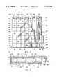
- FIG. 1is a fragmented schematic top view of a liquid crystal cell having opposed, patterned substrates that permit an electric field in conjunction with ultraviolet light to be used to selectively form walls.
- FIG. 2is a schematic, sectional side view of the display cell depicted in FIG. 1.
- FIG. 3is a schematic, sectional side view of the display cell of FIG. 1 wherein the cell is formed with plastic substrates.
- FIG. 4is a schematic, sectional side view of the display cell depicted in FIG. 1 being exposed to ultraviolet light while being subjected to an electric field.
- FIGS. 1-4An exemplary embodiment of a liquid crystal display cell having walls 8 formed by the method of the present invention using an electric field is depicted in FIGS. 1-4.
- a liquid crystal cellindicated generally by the numeral 10, includes an upper substrate 11 spaced from a lower substrate 12 by a plurality of plastic ball spacers 14.
- a liquid crystal mixture 16is also disposed between the substrates 11, 12.
- the upper substrate 11may be either transparent plastic or transparent glass depending on the desired application of the cell 10.
- the lower substrate 12may also be fabricated from plastic or glass, it may be fabricated from any of a variety of suitable materials because it typically does not have to be transparent.
- the upper substrate 11 depicted in FIG. 1is glass while the upper substrate 11 depicted in FIG. 3 is plastic.
- temporary external supports 18, 19may be used to maintain a constant distance between the plastic substrates 11, 12 while the walls 8 are formed.
- an electrically conductive coating 31, 32is formed in a preselected pattern on the inner surface 21, 22 of each substrate 11, 12.
- a transparent conductive coatingsuch as an Indium Tin Oxide (ITO) coating 31 is formed on the inner surface 21 of the upper substrate 11.
- ITOIndium Tin Oxide
- the transparent coating 31allows a person to view the liquid crystal mixture 16 through the coating 31 when the cell 10 is in use.
- the ITO coating 31may be created by any of the various methods known in the art.
- the coating on the lower substrate 12may also be formed from ITO but may also be any other conducting metal known in the art to be useful to form such coatings.
- the coatings 31, 32are formed in a selected pattern that ultimately determines the position of the support walls 8.
- the patterned coatingsmay be formed by any of the various methods known in this art.
- the patternis typically a grid arrangement that defines a plurality of pixels 40.
- the grid arrangementis created by providing a plurality of rows 42 on one of the substrates 11 and a plurality of columns 44 on the other substrate 12.
- Each pixel 40may thus be referred to by a row and column number.
- a plurality of plastic ball spacers 14 having an approximate diameter of 4.5 micrometersare dispersed on the substrates 11, 12.
- the spacers 14function to control the distance between the substrates 11, 12. It is generally desirable to disperse the ball spacers 14 evenly over the entire surface of each substrate 11, 12 by spin coating the ball spacers 14 onto the substrates 11, 12 at 2000 rpm for 30 seconds using a spin coater.
- One liquid crystal mixture 16 that has been found to function with the method of the present inventionis made up of 21% CE2, 21% CB15 and 58% E48 that is mixed with a UV curable monomer such as Norland 65 (NOA 65).
- the liquid crystal-monomer mixture 16may be in the approximate range of 10 percent to 40 percent by weight Norland 65. Preferably, the mixture is 15 percent by weight Norland 65. The mixture 16 is heated until it clears and mixes well.
- the cell 10is formed.
- the cell 10may be formed by pouring the liquid crystal-monomer mixture 16 on one of the substrates 11, 12 and placing the other substrate 11, 12 on top of the mixture. Pressure is then applied to the substrates 11, 12 by a roller which applies approximately 10 psi to the substrates 11, 12.
- a rollerwhich applies approximately 10 psi to the substrates 11, 12.
- other methods for forming the cell 10may also be used in conjunction with the concepts of the present invention.
- Another method of forming a cell 10is to place one of the substrates 11, 12 on top of the other substrate 11, 12 such that the ITO coatings 40 are facing each other. Either two or three of the edges are then sealed depending on the desired method of filling the space between the substrates 11, 12 with a liquid crystal-monomer mixture 16. When the space is filled by the method of capillary action, only two edges are initially sealed. When the vacuum method of filling is used, three edges are sealed to form a pocket. The edges may be sealed by applying a bead of ultraviolet (UV) curable epoxy to the edge and exposing the bead to ultraviolet light to form a seal 52. Such a seal 52 is only shown by way of example and is not always required.
- UVultraviolet
- the substrates 11, 12are offset approximately one eighth of an inch to provide a ledge 60 on two sides of the display cell 10.
- a conductive tape 62is then attached to each ledge 60 so that an electrical connection is formed between the tapes 62 and the conductive coatings 31, 32 on the substrates 11, 12.
- Lead wires 64are then attached to the tapes 62 so that each tape 62 may be connected to a power source (not shown).
- Individual electrical connections between the power source and each row 42 and column 44 of the conductive coatings 31, 32may also be formed to allow a person to exercise more control over the application of the electric field to the cell 10.
- each pixel 40it is desirable to form dividing walls 8 around each pixel 40 to compartmentalize each pixel in the display.
- the walls 8are formed by applying an electric field across the cell 10 which causes the monomer to separate into the low field regions 72.
- the cell 10is then exposed to UV light 70 until the dispersed monomer is polymerized to form the walls 8 in the low field regions 72.
- temperatures and voltagesmay be used to form the walls 8 only one preferred example and a general range are provided.
- One combination that has been found to be usefulis to expose the cell 10 while applying 50 Volts AC while maintaining the cell 10 at 65 degrees Celsius.
- the walls 8form in the low field, interpixel regions 72 around the high field, pixel regions 40.
- the fieldcould be from around 10 volts up to the tolerance of the cell 10.
- the temperaturemay be in the general range from room temperature up to the temperature limit of the cell 10.
- the walls 8may be formed using a mixture 16 made from a thermoplastic dispersed in a liquid crystal.
- a stock mixture of 21% CE2, 21% CB15 and 58% E48 liquid crystalis used to form the liquid-crystal mixture 50.
- This mixtureis first heated to approximately 100 degrees Celsius and stirred.
- a thermoplasticsuch as hydroxy functionalized polymethylmethacrylate supplied by Rohm and Hass is then mixed with the liquid crystal 16 and toluene is added to the mixture to assist the dispersion.
- the mixturemay include between 20% and 50% thermoplastic.
- the ITO coated substrates 11, 12are then cleaned with methanol and the ball spacers 14 are applied using a spin coater set at 2000 rpm for approximately 30 seconds.
- the liquid crystal-thermoplastic mixture 16is then spread on the open substrates 11, 12 and they are placed on a hot plate to evaporate the solvent.
- the two substrates 11, 12are then pressed together with the proper overlap to form the ledges 60.
- the substrates 11, 12may be pressed together for approximately 5 minutes with approximately 20 psi at 100 degrees Celsius.
- the substrates 11, 12are then removed from the hot plate and allowed to cool.
- the ledges 60are cleaned and conductive tapes 62 and lead wires 64 are applied.
- individual conductive tapes 62could be attached to each row 42 and each column 44 of conductive coating 31, 32 ifapprotional control were desired.
- the substrates 11, 12are then reheated to approximately 100 degrees Celsius while applying 30 Volts for approximately 15 minutes.
- the cell 10is then permitted to cool with the voltage applied. As the cell 10 cools, the thermoplastic hardens in the interpixel, low field regions 72 to form walls 8. The edges of the cell 10 may then be sealed with a UV curable epoxy if such a seal is desired.
Landscapes
- Physics & Mathematics (AREA)
- Nonlinear Science (AREA)
- Mathematical Physics (AREA)
- Chemical & Material Sciences (AREA)
- Crystallography & Structural Chemistry (AREA)
- General Physics & Mathematics (AREA)
- Optics & Photonics (AREA)
- Liquid Crystal (AREA)
Abstract
Description
The United States Government has a paid-up license in this invention and may have the right in limited circumstances to require the patent owner to license others on reasonable terms as provided for by the terms of Grant DMR89-20147, awarded by the National Science Foundation, and Contract No. N61331-94-K-0042, awarded by the advanced Research Projects Agency.
The present invention relates generally to a method for forming walls in a liquid crystal display cell. More particularly, the present invention is directed to a method for forming walls in a liquid crystal display cell by dissolving a polymerizable monomer in a liquid crystal and selectively curing the monomer to form the support walls. Specifically, the monomer is selectively cured by applying a patterned electric field to the liquid crystal-monomer mixture and exposing the mixture to ultraviolet light causing walls to form in the low-field interpixel regions.
A typical liquid crystal display cell includes a liquid crystal sealed between two substrates. A plurality of spacers may be disposed between the substrates to maintain a constant distance between the substrates. When assembled, the internal pressure of the device may be lowered to below atmospheric such that the substrates are forced in contact with the spacers. In such an application, the substrates are relatively rigid in order to prevent the substrates from bending in the expanses between the spacers. The combination of the negative pressure and the rigidity of the glass substrates causes the distance between the substrates to be maintained even when external forces such as pinching and bending act on the display device.
In addition to the spacers, it is often desirable to provide cell walls between the substrates. A cell wall generally refers to any structure extending between substrates of the cell. The walls may be used for maintaining a constant distance between the substrates or for segregating the cell into different areas. When used to segregate, the walls prevent liquid crystal flow between selected areas of a cell. Cell walls may also be useful for preventing expansion caused by gas bubbles that diffuse through the substrate or from the liquid crystal itself.
Known processes for forming cell walls in a liquid crystal display often include undesirable steps. For instance, when the masking method is used to form the walls, the mask must be perfectly formed and perfectly aligned so that the cell walls are properly formed. These steps require precision and are time consuming. Further, perfect alignment is especially problematic when one desires to form a cell wall around each individual pixel in a liquid crystal display. The masking method is also difficult to employ with thick substrates due to the bending of light that occurs through the thick substrate. It is thus desirable to provide a method for forming walls in a liquid crystal display cell that results in accurately formed walls. It is highly desirable that the method of forming the walls does not require the step of individually selecting the walls to be formed and individually segregating the walls.
In view of the foregoing, an object of the present invention is to provide a method for forming walls between substrates in a liquid crystal display cell.
Another object of the present invention is to provide a method, as above, that includes the use of polymerizable monomer units that are dissolved in the liquid crystal in the display cell and are selectively polymerized by exposing the cell to ultraviolet light.
Yet another object of the present invention is to provide a method, as above, that includes the use of a thermoplastic dissolved in the liquid crystal in the display device which is selectively hardened by reducing the temperature of a cell while applying a patterned electric field to the cell.
Still another object of the present invention is to provide a method, as above, to selectively polymerize the monomer units by applying a patterned electric field through the liquid crystal-monomer mixture to separate the monomer units into the low field regions and then exposing the mixture to ultraviolet light until the monomer polymerizes to form the walls in the low field regions.
Another object of the present invention is to provide a method, as above, that automatically forms walls around the individual electrodes of the display cell.
These and other objects of the invention, as well as the advantages thereof over existing in prior art forms, which will be apparent in view of the following detailed specification, are accomplished by means hereinafter described and claimed.
In general, a method for forming walls in a liquid crystal cell includes the steps of providing a liquid crystal display cell having a liquid crystal-monomer mixture disposed between patterned electrically conductive coatings, applying an electric field across the cell to form low-field and high-field regions, and exposing the cell to ultraviolet light until polymer walls form in the low-field regions.
Another aspect of the present invention is achieved by a method including the steps of providing upper and lower substrates; forming patterned, electrically conductive coatings on each of the substrates; adding a liquid crystal monomer mixture to one of the substrates over the coating; positioning the other substrate over the mixture such that the coating contacts the mixture; applying an electric field to the mixture until the monomer separates to the low field regions; and exposing the substrates and mixture to ultraviolet light until the monomer polymerizes to form support walls in the low-field regions.
To acquaint persons skilled in the art most closely related to the present invention, one preferred embodiment and one alternative embodiment of a method for forming liquid crystal display cell walls using a patterned electric field is disclosed herein by, and with reference to the annexed drawings that form a part of the specification. The exemplary method is described in detail without attempting to show all of the various forms and modifications in which the invention might be embodied. As such, the embodiments shown and described herein are illustrative, and as will become apparent to those skilled in the art, can be modified in numerous ways within the spirit and scope of the invention; the invention being defined by the appended claims and their equivalent embodiments.
FIG. 1 is a fragmented schematic top view of a liquid crystal cell having opposed, patterned substrates that permit an electric field in conjunction with ultraviolet light to be used to selectively form walls.
FIG. 2 is a schematic, sectional side view of the display cell depicted in FIG. 1.
FIG. 3 is a schematic, sectional side view of the display cell of FIG. 1 wherein the cell is formed with plastic substrates.
FIG. 4 is a schematic, sectional side view of the display cell depicted in FIG. 1 being exposed to ultraviolet light while being subjected to an electric field.
An exemplary embodiment of a liquid crystal displaycell having walls 8 formed by the method of the present invention using an electric field is depicted in FIGS. 1-4. A liquid crystal cell, indicated generally by thenumeral 10, includes anupper substrate 11 spaced from alower substrate 12 by a plurality ofplastic ball spacers 14. Aliquid crystal mixture 16 is also disposed between thesubstrates upper substrate 11 may be either transparent plastic or transparent glass depending on the desired application of thecell 10. Although thelower substrate 12 may also be fabricated from plastic or glass, it may be fabricated from any of a variety of suitable materials because it typically does not have to be transparent. Theupper substrate 11 depicted in FIG. 1 is glass while theupper substrate 11 depicted in FIG. 3 is plastic. Whenplastic substrates cell 10, temporaryexternal supports plastic substrates walls 8 are formed.
When using an electric field to form thesupport walls 8, an electricallyconductive coating inner surface substrate cell 10 is viewed through theupper substrate 11 and thus a transparent conductive coating such as an Indium Tin Oxide (ITO)coating 31 is formed on theinner surface 21 of theupper substrate 11. Thetransparent coating 31 allows a person to view theliquid crystal mixture 16 through thecoating 31 when thecell 10 is in use. The ITOcoating 31 may be created by any of the various methods known in the art. The coating on thelower substrate 12 may also be formed from ITO but may also be any other conducting metal known in the art to be useful to form such coatings.
Thecoatings support walls 8. The patterned coatings may be formed by any of the various methods known in this art. As may be seen in FIG. 1, the pattern is typically a grid arrangement that defines a plurality ofpixels 40. The grid arrangement is created by providing a plurality ofrows 42 on one of thesubstrates 11 and a plurality ofcolumns 44 on theother substrate 12. Eachpixel 40 may thus be referred to by a row and column number.
After theconductive coatings plastic ball spacers 14 having an approximate diameter of 4.5 micrometers are dispersed on thesubstrates spacers 14 function to control the distance between thesubstrates ball spacers 14 evenly over the entire surface of eachsubstrate ball spacers 14 onto thesubstrates
Oneliquid crystal mixture 16 that has been found to function with the method of the present invention is made up of 21% CE2, 21% CB15 and 58% E48 that is mixed with a UV curable monomer such as Norland 65 (NOA 65). The liquid crystal-monomer mixture 16 may be in the approximate range of 10 percent to 40 percent by weight Norland 65. Preferably, the mixture is 15 percent by weight Norland 65. Themixture 16 is heated until it clears and mixes well.
After the ball spacers 14 have been dispersed, thecell 10 is formed. Thecell 10 may be formed by pouring the liquid crystal-monomer mixture 16 on one of thesubstrates other substrate substrates substrates cell 10 may also be used in conjunction with the concepts of the present invention.
Another method of forming acell 10 is to place one of thesubstrates other substrate ITO coatings 40 are facing each other. Either two or three of the edges are then sealed depending on the desired method of filling the space between thesubstrates monomer mixture 16. When the space is filled by the method of capillary action, only two edges are initially sealed. When the vacuum method of filling is used, three edges are sealed to form a pocket. The edges may be sealed by applying a bead of ultraviolet (UV) curable epoxy to the edge and exposing the bead to ultraviolet light to form aseal 52. Such aseal 52 is only shown by way of example and is not always required.
When thecell 10 is assembled, thesubstrates ledge 60 on two sides of thedisplay cell 10. Aconductive tape 62 is then attached to eachledge 60 so that an electrical connection is formed between thetapes 62 and theconductive coatings substrates wires 64 are then attached to thetapes 62 so that eachtape 62 may be connected to a power source (not shown). Individual electrical connections between the power source and eachrow 42 andcolumn 44 of theconductive coatings cell 10.
Generally, it is desirable to form dividingwalls 8 around eachpixel 40 to compartmentalize each pixel in the display. Thewalls 8 are formed by applying an electric field across thecell 10 which causes the monomer to separate into thelow field regions 72. Thecell 10 is then exposed toUV light 70 until the dispersed monomer is polymerized to form thewalls 8 in thelow field regions 72. Although various combinations of temperatures and voltages may be used to form thewalls 8, only one preferred example and a general range are provided. Those skilled in the art will appreciate that numerous combinations may be used to create thewalls 8 in accordance with the method of the present invention. One combination that has been found to be useful is to expose thecell 10 while applying 50 Volts AC while maintaining thecell 10 at 65 degrees Celsius. As thecell 10 is exposed, thewalls 8 form in the low field,interpixel regions 72 around the high field,pixel regions 40. It is also known that the field could be from around 10 volts up to the tolerance of thecell 10. It is also known that the temperature may be in the general range from room temperature up to the temperature limit of thecell 10.
It has also been found that thewalls 8 may be formed using amixture 16 made from a thermoplastic dispersed in a liquid crystal. To formsuch walls 8, a stock mixture of 21% CE2, 21% CB15 and 58% E48 liquid crystal is used to form the liquid-crystal mixture 50. This mixture is first heated to approximately 100 degrees Celsius and stirred. A thermoplastic such as hydroxy functionalized polymethylmethacrylate supplied by Rohm and Hass is then mixed with theliquid crystal 16 and toluene is added to the mixture to assist the dispersion. The mixture may include between 20% and 50% thermoplastic.
The ITO coatedsubstrates thermoplastic mixture 16 is then spread on theopen substrates substrates ledges 60. For example, thesubstrates substrates ledges 60 are cleaned andconductive tapes 62 andlead wires 64 are applied. As explained above, individualconductive tapes 62 could be attached to eachrow 42 and eachcolumn 44 ofconductive coating substrates cell 10 is then permitted to cool with the voltage applied. As thecell 10 cools, the thermoplastic hardens in the interpixel,low field regions 72 to formwalls 8. The edges of thecell 10 may then be sealed with a UV curable epoxy if such a seal is desired.
While only a preferred embodiment of the present invention is disclosed, it is to be clearly understood that the same is susceptible to numerous modifications apparent to one skilled in the art. For instance, the descriptions of the liquid crystals, the monomers, and the thermoplastics are for exemplary purposes only and it is contemplated that other substances known to those skilled in the art may be substituted for the examples shown. The same may also be said for the exemplary temperatures and times described. Therefore, the scope of the present invention is not to be limited to the details shown and described but is intended to include all changes and modifications which come within the scope of the appended claims and their equivalents.
Claims (11)
1. A method for forming walls in situ in a liquid crystal display cell comprising the steps of:
providing a liquid crystal display cell having a liquid crystal-monomer mixture disposed between patterned electrically conductive coatings on opposed substrates, wherein an intersection of the patterned electrically conductive coatings forms a pixel region;
applying a voltage across the cell to form a high-field region between the substrates in said pixel region and a low field region elsewhere such that the monomer separates into said low field region; and
exposing the cell to ultraviolet light until polymer walls form in the low-field regions between the substrates.
2. A method according to claim 1, wherein the step of providing a liquid crystal cell comprises the steps of:
providing upper and lower substrates;
applying a patterned electrically conductive coating to each substrate;
adding a liquid crystal monomer mixture to one of the substrates; and
forming the cell by placing one of the substrates over the other substrate.
3. A method according to claim 2, further comprising the step of offsetting one substrate to form a pair of ledges.
4. A method according to claim 3, further comprising the step of attaching a conductive tape to the ledge such that the tape forms an electrical connection with the conductive coating.
5. A method according to claim 2, further comprising the step of sealing the edges of the cell.
6. A method according to claim 1, further comprising the step of heating the cell to substantially 65 degrees celsius.
7. A method according to claim 1, further comprising the step of applying 50 volts AC to the cell.
8. A method for forming walls in situ in a liquid crystal display cell comprising the steps of:
providing upper and lower substrates;
forming patterned, electrically conductive coatings on each of the substrates, wherein an intersection of the patterned electrically conductive coatings forms a pixel region;
adding a liquid crystal-monomer mixture to one of the substrates over the coating;
positioning the other substrate over the mixture such that the coating contacts the mixture;
applying a voltage across the mixture to form a high field region between the substrates in said pixel region and a low field region elsewhere such that the monomer separates into said low field region; and
exposing the mixture to ultraviolet light until walls form in the low-field regions between the substrates.
9. A method according to claim 8, further comprising the step of dispersing ball spacers on the substrates before the mixture is added.
10. A method according to claim 8, further comprising the steps of:
forming a row pattern of conductive coating on one of the substrates and a column pattern of conductive coating on the other substrate; and
assembling the substrates so that the row pattern and column pattern cooperate to form a grid pattern.
11. A method for forming walls in situ in a liquid crystal cell comprising the steps of:
providing upper and lower substrates;
forming patterned, electrically conductive coatings on each of the substrates, wherein an intersection of the patterned electrically conductive coatings forms a pixel region;
adding a liquid crystal-thermoplastic mixture to one of the substrates over the coating;
positioning the other substrate over the mixture such that the coating contacts the mixture;
heating the mixture;
applying an electric field across the mixture to form a high field region between the substrates in said pixel region and a low field region elsewhere such that the thermoplastic separates into said low field region; and
cooling the mixture until the thermoplastic hardens in the low field regions to form walls between the substrates.
Priority Applications (1)
| Application Number | Priority Date | Filing Date | Title |
|---|---|---|---|
| US08/953,596US5929960A (en) | 1997-10-17 | 1997-10-17 | Method for forming liquid crystal display cell walls using a patterned electric field |
Applications Claiming Priority (1)
| Application Number | Priority Date | Filing Date | Title |
|---|---|---|---|
| US08/953,596US5929960A (en) | 1997-10-17 | 1997-10-17 | Method for forming liquid crystal display cell walls using a patterned electric field |
Publications (1)
| Publication Number | Publication Date |
|---|---|
| US5929960Atrue US5929960A (en) | 1999-07-27 |
Family
ID=25494233
Family Applications (1)
| Application Number | Title | Priority Date | Filing Date |
|---|---|---|---|
| US08/953,596Expired - LifetimeUS5929960A (en) | 1997-10-17 | 1997-10-17 | Method for forming liquid crystal display cell walls using a patterned electric field |
Country Status (1)
| Country | Link |
|---|---|
| US (1) | US5929960A (en) |
Cited By (73)
| Publication number | Priority date | Publication date | Assignee | Title |
|---|---|---|---|---|
| US6285382B1 (en)* | 1998-03-13 | 2001-09-04 | Sharp Kabushiki Kaisha | Recording medium and image forming apparatus for forming image thereon |
| US6356335B1 (en)* | 1998-11-11 | 2002-03-12 | Lg. Phillips Lcd Co., Ltd. | Multi-domain liquid crystal display device |
| US20030193709A1 (en)* | 2002-03-27 | 2003-10-16 | Prakash Mallya | Switchable electro-optical laminates |
| US20030205632A1 (en)* | 2000-07-25 | 2003-11-06 | Chang-Jin Kim | Electrowetting-driven micropumping |
| US20040246406A1 (en)* | 2001-10-02 | 2004-12-09 | Fujitsu Display Technologies Corporation | Liquid crystal display device and method of fabricating the same |
| US20050052609A1 (en)* | 2003-09-10 | 2005-03-10 | Ci-Ling Pan | Multi-wavelength external-cavity laser with digital and mode-hope-free fine tuning mechanisms |
| WO2005050297A1 (en)* | 2003-11-22 | 2005-06-02 | Koninklijke Philips Electronics N.V. | Active matrix display device and method of producing the same |
| JP2005177971A (en)* | 2003-11-26 | 2005-07-07 | Ricoh Co Ltd | Plastic molding product manufacturing method, manufacturing apparatus, and plastic molding product manufactured by the manufacturing method |
| US20050258573A1 (en)* | 2004-05-18 | 2005-11-24 | Daiki Minegishi | Method and device for fabricating plastic molded article |
| US20070217956A1 (en)* | 2002-09-24 | 2007-09-20 | Pamula Vamsee K | Methods for nucleic acid amplification on a printed circuit board |
| US20070291385A1 (en)* | 2006-06-20 | 2007-12-20 | Lg.Philips Lcd Co., Ltd. | Color filter substrate for liquid crystal display device and method for fabricating the same |
| CN100380192C (en)* | 2005-07-14 | 2008-04-09 | 友达光电股份有限公司 | Liquid crystal display device and manufacturing method thereof |
| US20080247920A1 (en)* | 2002-09-24 | 2008-10-09 | Duke University | Apparatus for Manipulating Droplets |
| US20080316406A1 (en)* | 2001-10-02 | 2008-12-25 | Sharp Kabushiki Kaisha | Liquid crystal display device and method of fabricating the same |
| US20090097116A1 (en)* | 2005-08-15 | 2009-04-16 | Isis Innovation Limited | Optical Element and Method of Production |
| US20100126860A1 (en)* | 2007-08-09 | 2010-05-27 | Advanced Liquid Logic, Inc. | PCB Droplet Actuator Fabrication |
| CN101482679B (en)* | 2001-10-02 | 2012-02-22 | 夏普株式会社 | Liquid crystal display device and manufacturing method thereof |
| US8147668B2 (en) | 2002-09-24 | 2012-04-03 | Duke University | Apparatus for manipulating droplets |
| US9334425B2 (en) | 2009-03-30 | 2016-05-10 | Avery Dennison Corporation | Removable adhesive label containing high tensile modulus polymeric film layer |
| US9387652B2 (en) | 2005-01-10 | 2016-07-12 | Avery Dennison Corporation | Removable curl labels |
| US9422465B2 (en) | 2006-11-02 | 2016-08-23 | Avery Dennison Corporation | Emulsion adhesive for washable film |
| US10002549B2 (en) | 2009-03-30 | 2018-06-19 | Avery Dennison Corporation | Removable adhesive label containing polymeric film layer having water affinity |
| US10089516B2 (en) | 2013-07-31 | 2018-10-02 | Digilens, Inc. | Method and apparatus for contact image sensing |
| US10114251B2 (en) | 2015-12-17 | 2018-10-30 | A.U. Vista, Inc. | Liquid crystal display having holding member and method of fabricating same |
| US10145533B2 (en) | 2005-11-11 | 2018-12-04 | Digilens, Inc. | Compact holographic illumination device |
| US10156681B2 (en) | 2015-02-12 | 2018-12-18 | Digilens Inc. | Waveguide grating device |
| US10157554B2 (en) | 2009-03-30 | 2018-12-18 | Avery Dennison Corporation | Removable adhesive label containing inherently shrinkable polymeric film |
| US10185154B2 (en) | 2011-04-07 | 2019-01-22 | Digilens, Inc. | Laser despeckler based on angular diversity |
| US10209517B2 (en) | 2013-05-20 | 2019-02-19 | Digilens, Inc. | Holographic waveguide eye tracker |
| US10216061B2 (en) | 2012-01-06 | 2019-02-26 | Digilens, Inc. | Contact image sensor using switchable bragg gratings |
| WO2019041729A1 (en)* | 2017-08-31 | 2019-03-07 | Boe Technology Group Co., Ltd. | Display panel having black matrix comprising linear polarizer layer and fabricating method thereof |
| US10234696B2 (en) | 2007-07-26 | 2019-03-19 | Digilens, Inc. | Optical apparatus for recording a holographic device and method of recording |
| US10241330B2 (en) | 2014-09-19 | 2019-03-26 | Digilens, Inc. | Method and apparatus for generating input images for holographic waveguide displays |
| US10330777B2 (en) | 2015-01-20 | 2019-06-25 | Digilens Inc. | Holographic waveguide lidar |
| US10359736B2 (en) | 2014-08-08 | 2019-07-23 | Digilens Inc. | Method for holographic mastering and replication |
| US10423222B2 (en) | 2014-09-26 | 2019-09-24 | Digilens Inc. | Holographic waveguide optical tracker |
| US10437051B2 (en) | 2012-05-11 | 2019-10-08 | Digilens Inc. | Apparatus for eye tracking |
| US10437064B2 (en) | 2015-01-12 | 2019-10-08 | Digilens Inc. | Environmentally isolated waveguide display |
| US10459145B2 (en) | 2015-03-16 | 2019-10-29 | Digilens Inc. | Waveguide device incorporating a light pipe |
| US10545346B2 (en) | 2017-01-05 | 2020-01-28 | Digilens Inc. | Wearable heads up displays |
| US10591756B2 (en) | 2015-03-31 | 2020-03-17 | Digilens Inc. | Method and apparatus for contact image sensing |
| US10642058B2 (en) | 2011-08-24 | 2020-05-05 | Digilens Inc. | Wearable data display |
| US10670876B2 (en) | 2011-08-24 | 2020-06-02 | Digilens Inc. | Waveguide laser illuminator incorporating a despeckler |
| US10678053B2 (en) | 2009-04-27 | 2020-06-09 | Digilens Inc. | Diffractive projection apparatus |
| US10690916B2 (en) | 2015-10-05 | 2020-06-23 | Digilens Inc. | Apparatus for providing waveguide displays with two-dimensional pupil expansion |
| US10690851B2 (en) | 2018-03-16 | 2020-06-23 | Digilens Inc. | Holographic waveguides incorporating birefringence control and methods for their fabrication |
| US10732569B2 (en) | 2018-01-08 | 2020-08-04 | Digilens Inc. | Systems and methods for high-throughput recording of holographic gratings in waveguide cells |
| US10859768B2 (en) | 2016-03-24 | 2020-12-08 | Digilens Inc. | Method and apparatus for providing a polarization selective holographic waveguide device |
| US10890707B2 (en) | 2016-04-11 | 2021-01-12 | Digilens Inc. | Holographic waveguide apparatus for structured light projection |
| US10914950B2 (en) | 2018-01-08 | 2021-02-09 | Digilens Inc. | Waveguide architectures and related methods of manufacturing |
| US10942430B2 (en) | 2017-10-16 | 2021-03-09 | Digilens Inc. | Systems and methods for multiplying the image resolution of a pixelated display |
| US10983340B2 (en) | 2016-02-04 | 2021-04-20 | Digilens Inc. | Holographic waveguide optical tracker |
| WO2021082102A1 (en)* | 2019-10-28 | 2021-05-06 | 武汉华星光电技术有限公司 | Display panel and manufacturing method therefor |
| US11307432B2 (en) | 2014-08-08 | 2022-04-19 | Digilens Inc. | Waveguide laser illuminator incorporating a Despeckler |
| US11378732B2 (en) | 2019-03-12 | 2022-07-05 | DigLens Inc. | Holographic waveguide backlight and related methods of manufacturing |
| US11402801B2 (en) | 2018-07-25 | 2022-08-02 | Digilens Inc. | Systems and methods for fabricating a multilayer optical structure |
| US11442222B2 (en) | 2019-08-29 | 2022-09-13 | Digilens Inc. | Evacuated gratings and methods of manufacturing |
| US11448937B2 (en) | 2012-11-16 | 2022-09-20 | Digilens Inc. | Transparent waveguide display for tiling a display having plural optical powers using overlapping and offset FOV tiles |
| US11460621B2 (en) | 2012-04-25 | 2022-10-04 | Rockwell Collins, Inc. | Holographic wide angle display |
| US11480788B2 (en) | 2015-01-12 | 2022-10-25 | Digilens Inc. | Light field displays incorporating holographic waveguides |
| US11513350B2 (en) | 2016-12-02 | 2022-11-29 | Digilens Inc. | Waveguide device with uniform output illumination |
| US11543594B2 (en) | 2019-02-15 | 2023-01-03 | Digilens Inc. | Methods and apparatuses for providing a holographic waveguide display using integrated gratings |
| US11681143B2 (en) | 2019-07-29 | 2023-06-20 | Digilens Inc. | Methods and apparatus for multiplying the image resolution and field-of-view of a pixelated display |
| US11726332B2 (en) | 2009-04-27 | 2023-08-15 | Digilens Inc. | Diffractive projection apparatus |
| US11747568B2 (en) | 2019-06-07 | 2023-09-05 | Digilens Inc. | Waveguides incorporating transmissive and reflective gratings and related methods of manufacturing |
| US12092914B2 (en) | 2018-01-08 | 2024-09-17 | Digilens Inc. | Systems and methods for manufacturing waveguide cells |
| US12140764B2 (en) | 2019-02-15 | 2024-11-12 | Digilens Inc. | Wide angle waveguide display |
| US12158612B2 (en) | 2021-03-05 | 2024-12-03 | Digilens Inc. | Evacuated periodic structures and methods of manufacturing |
| US12210153B2 (en) | 2019-01-14 | 2025-01-28 | Digilens Inc. | Holographic waveguide display with light control layer |
| US12222499B2 (en) | 2020-12-21 | 2025-02-11 | Digilens Inc. | Eye glow suppression in waveguide based displays |
| US12306585B2 (en) | 2018-01-08 | 2025-05-20 | Digilens Inc. | Methods for fabricating optical waveguides |
| US12399326B2 (en) | 2021-01-07 | 2025-08-26 | Digilens Inc. | Grating structures for color waveguides |
| US12397477B2 (en) | 2019-02-05 | 2025-08-26 | Digilens Inc. | Methods for compensating for optical surface nonuniformity |
Citations (13)
| Publication number | Priority date | Publication date | Assignee | Title |
|---|---|---|---|---|
| US3863332A (en)* | 1973-06-28 | 1975-02-04 | Hughes Aircraft Co | Method of fabricating back panel for liquid crystal display |
| US4295712A (en)* | 1978-08-18 | 1981-10-20 | Canon Kabushiki Kaisha | Liquid crystal display device |
| US4636785A (en)* | 1983-03-23 | 1987-01-13 | Thomson-Csf | Indicator device with electric control of displacement of a fluid |
| US4653864A (en)* | 1986-02-26 | 1987-03-31 | Ovonic Imaging Systems, Inc. | Liquid crystal matrix display having improved spacers and method of making same |
| US4682858A (en)* | 1984-08-20 | 1987-07-28 | Canon Kabushiki Kaisha | Liquid crystal device having reduced-pressure region in communication with ferroelectric liquid crystal |
| US4705360A (en)* | 1982-10-29 | 1987-11-10 | Sharp Kabushiki Kaisha | Liquid crystal display cell and method for manufacturing thereof |
| US4900132A (en)* | 1987-04-13 | 1990-02-13 | Tektronix, Inc. | Chiral liquid crystal cell |
| US4973138A (en)* | 1987-10-27 | 1990-11-27 | Semiconductor Energy Laboratory Co., Ltd. | Liquid crystal device and manufacturing method for the same |
| US5231527A (en)* | 1991-02-01 | 1993-07-27 | Sharp Kabushiki Kaisha | Liquid crystal display with spacer having elastic modulus in compression of 370-550 kg/mm2 at 10% displacement of diameter |
| US5385499A (en)* | 1992-01-30 | 1995-01-31 | Futaba Denshi Kogyo K.K. | Envelope for display device and method for manufacturing same |
| US5459598A (en)* | 1992-01-15 | 1995-10-17 | Thorn Emi Plc | Optical modulation device with liquid crystal voids formed by the spacer arrangements |
| US5530567A (en)* | 1993-06-29 | 1996-06-25 | Casio Computer Co., Ltd. | Polymer dispersed liquid crystal display device having encapsulated liquid crystal surrounded by polymer matrix liquid crystal and method of manufacturing the same |
| US5627665A (en)* | 1993-07-15 | 1997-05-06 | Sharp Kabushiki Kaisha | Liquid crystal display device and method for producing the same |
- 1997
- 1997-10-17USUS08/953,596patent/US5929960A/ennot_activeExpired - Lifetime
Patent Citations (13)
| Publication number | Priority date | Publication date | Assignee | Title |
|---|---|---|---|---|
| US3863332A (en)* | 1973-06-28 | 1975-02-04 | Hughes Aircraft Co | Method of fabricating back panel for liquid crystal display |
| US4295712A (en)* | 1978-08-18 | 1981-10-20 | Canon Kabushiki Kaisha | Liquid crystal display device |
| US4705360A (en)* | 1982-10-29 | 1987-11-10 | Sharp Kabushiki Kaisha | Liquid crystal display cell and method for manufacturing thereof |
| US4636785A (en)* | 1983-03-23 | 1987-01-13 | Thomson-Csf | Indicator device with electric control of displacement of a fluid |
| US4682858A (en)* | 1984-08-20 | 1987-07-28 | Canon Kabushiki Kaisha | Liquid crystal device having reduced-pressure region in communication with ferroelectric liquid crystal |
| US4653864A (en)* | 1986-02-26 | 1987-03-31 | Ovonic Imaging Systems, Inc. | Liquid crystal matrix display having improved spacers and method of making same |
| US4900132A (en)* | 1987-04-13 | 1990-02-13 | Tektronix, Inc. | Chiral liquid crystal cell |
| US4973138A (en)* | 1987-10-27 | 1990-11-27 | Semiconductor Energy Laboratory Co., Ltd. | Liquid crystal device and manufacturing method for the same |
| US5231527A (en)* | 1991-02-01 | 1993-07-27 | Sharp Kabushiki Kaisha | Liquid crystal display with spacer having elastic modulus in compression of 370-550 kg/mm2 at 10% displacement of diameter |
| US5459598A (en)* | 1992-01-15 | 1995-10-17 | Thorn Emi Plc | Optical modulation device with liquid crystal voids formed by the spacer arrangements |
| US5385499A (en)* | 1992-01-30 | 1995-01-31 | Futaba Denshi Kogyo K.K. | Envelope for display device and method for manufacturing same |
| US5530567A (en)* | 1993-06-29 | 1996-06-25 | Casio Computer Co., Ltd. | Polymer dispersed liquid crystal display device having encapsulated liquid crystal surrounded by polymer matrix liquid crystal and method of manufacturing the same |
| US5627665A (en)* | 1993-07-15 | 1997-05-06 | Sharp Kabushiki Kaisha | Liquid crystal display device and method for producing the same |
Non-Patent Citations (7)
| Title |
|---|
| Late News Poster: Axially Symmetric Aligned Microcell (ASM) Mode: Electro Optical Characteristics of New Display Mode with Excellent Wide Viewing Angle, SID Digest, SID 95 Digest (1995), pp. 575 578.* |
| Late-News Poster: Axially Symmetric Aligned Microcell (ASM) Mode: Electro-Optical Characteristics of New Display Mode with Excellent Wide Viewing Angle, SID Digest, SID 95 Digest (1995), pp. 575-578. |
| Patent Abstracts of Japan, JP 07072461 A, Liquid Crystal Display Device and its Manufacture, Tomita et al., Jan. 28, 1985.* |
| Patent Abstracts of Japan, JP 08320470 A2; Liquid Crystal Optical device and its Manufactured, Yuasa et al., May 25, 1995.* |
| Patent Abstracts of Japan, JP 61173221 A, Formation of Liquid Crystal Display Device, Shunpei et al., Jan. 28, 1985.* |
| The Classical Theory of Electricity and Magnetism, Max Abraham (1950), pp. 80 108.* |
| The Classical Theory of Electricity and Magnetism, Max Abraham (1950), pp. 80-108. |
Cited By (147)
| Publication number | Priority date | Publication date | Assignee | Title |
|---|---|---|---|---|
| US6285382B1 (en)* | 1998-03-13 | 2001-09-04 | Sharp Kabushiki Kaisha | Recording medium and image forming apparatus for forming image thereon |
| US6356335B1 (en)* | 1998-11-11 | 2002-03-12 | Lg. Phillips Lcd Co., Ltd. | Multi-domain liquid crystal display device |
| US8529743B2 (en)* | 2000-07-25 | 2013-09-10 | The Regents Of The University Of California | Electrowetting-driven micropumping |
| US20030205632A1 (en)* | 2000-07-25 | 2003-11-06 | Chang-Jin Kim | Electrowetting-driven micropumping |
| US8558959B2 (en) | 2001-10-02 | 2013-10-15 | Sharp Kabushiki Kaisha | Liquid crystal display device and method of fabricating the same |
| US20080316406A1 (en)* | 2001-10-02 | 2008-12-25 | Sharp Kabushiki Kaisha | Liquid crystal display device and method of fabricating the same |
| US20050018105A1 (en)* | 2001-10-02 | 2005-01-27 | Fujitsu Display Technologies Corporation | Liquid crystal display device and method of fabricating the same |
| US20050024556A1 (en)* | 2001-10-02 | 2005-02-03 | Fujitsu Display Technologies Corporation | Liquid crystal display device and method of fabricating the same |
| US20050030445A1 (en)* | 2001-10-02 | 2005-02-10 | Fujitsu Display Technologies Corporation | Liquid crystal display device and method of fabricating the same |
| US20040246406A1 (en)* | 2001-10-02 | 2004-12-09 | Fujitsu Display Technologies Corporation | Liquid crystal display device and method of fabricating the same |
| US20040263719A1 (en)* | 2001-10-02 | 2004-12-30 | Fujitsu Display Technologies Corporation | Liquid crystal display device and method of fabricating the same |
| US6894742B2 (en)* | 2001-10-02 | 2005-05-17 | Fujitsu Display Technologies Corporation | Liquid crystal display device and method of fabricating the same |
| US7450206B2 (en) | 2001-10-02 | 2008-11-11 | Sharp Kabushiki Kaisha | Liquid crystal display device and method of fabricating the same |
| US7324175B2 (en) | 2001-10-02 | 2008-01-29 | Sharp Kabushiki Kaisha | Liquid crystal display device and method of fabricating the same |
| US6937300B2 (en)* | 2001-10-02 | 2005-08-30 | Fujitsu Display Technologies Corporation | Liquid crystal display device and method of fabricating the same |
| CN100474089C (en)* | 2001-10-02 | 2009-04-01 | 夏普株式会社 | Liquid crystal display device and method of fabricating the same |
| US8284362B2 (en) | 2001-10-02 | 2012-10-09 | Sharp Kabushiki Kaisha | Liquid crystal display device and method of fabricating the same |
| US20110058134A1 (en)* | 2001-10-02 | 2011-03-10 | Sharp Kabushiki Kaisha | Liquid crystal display device and method of fabricating the same |
| US7136119B2 (en) | 2001-10-02 | 2006-11-14 | Sharp Kabushiki Kaisha | Liquid crystal display device and method of fabricating the same |
| CN101482679B (en)* | 2001-10-02 | 2012-02-22 | 夏普株式会社 | Liquid crystal display device and manufacturing method thereof |
| US7956969B2 (en) | 2001-10-02 | 2011-06-07 | Sharp Kabushiki Kaisha | Liquid crystal display device |
| US20050083564A1 (en)* | 2002-03-27 | 2005-04-21 | Prakash Mallya | Switchable electro-optical laminates |
| US7023600B2 (en) | 2002-03-27 | 2006-04-04 | Avery Dennison Corporation | Switchable electro-optical laminates |
| US6963435B2 (en) | 2002-03-27 | 2005-11-08 | Avery Dennison Corporation | Switchable electro-optical laminates |
| US20030193709A1 (en)* | 2002-03-27 | 2003-10-16 | Prakash Mallya | Switchable electro-optical laminates |
| US8394249B2 (en) | 2002-09-24 | 2013-03-12 | Duke University | Methods for manipulating droplets by electrowetting-based techniques |
| US8871071B2 (en) | 2002-09-24 | 2014-10-28 | Duke University | Droplet manipulation device |
| US20080247920A1 (en)* | 2002-09-24 | 2008-10-09 | Duke University | Apparatus for Manipulating Droplets |
| US9638662B2 (en) | 2002-09-24 | 2017-05-02 | Duke University | Apparatuses and methods for manipulating droplets |
| US9180450B2 (en) | 2002-09-24 | 2015-11-10 | Advanced Liquid Logic, Inc. | Droplet manipulation system and method |
| US20100025242A1 (en)* | 2002-09-24 | 2010-02-04 | Duke University | Apparatuses and methods for manipulating droplets |
| US9110017B2 (en) | 2002-09-24 | 2015-08-18 | Duke University | Apparatuses and methods for manipulating droplets |
| US8906627B2 (en) | 2002-09-24 | 2014-12-09 | Duke University | Apparatuses and methods for manipulating droplets |
| US20080264797A1 (en)* | 2002-09-24 | 2008-10-30 | Duke University | Apparatus for Manipulating Droplets |
| US8048628B2 (en) | 2002-09-24 | 2011-11-01 | Duke University | Methods for nucleic acid amplification on a printed circuit board |
| US8524506B2 (en) | 2002-09-24 | 2013-09-03 | Duke University | Methods for sampling a liquid flow |
| US20070217956A1 (en)* | 2002-09-24 | 2007-09-20 | Pamula Vamsee K | Methods for nucleic acid amplification on a printed circuit board |
| US8147668B2 (en) | 2002-09-24 | 2012-04-03 | Duke University | Apparatus for manipulating droplets |
| US8221605B2 (en) | 2002-09-24 | 2012-07-17 | Duke University | Apparatus for manipulating droplets |
| US8388909B2 (en) | 2002-09-24 | 2013-03-05 | Duke University | Apparatuses and methods for manipulating droplets |
| US8349276B2 (en) | 2002-09-24 | 2013-01-08 | Duke University | Apparatuses and methods for manipulating droplets on a printed circuit board |
| US20050052609A1 (en)* | 2003-09-10 | 2005-03-10 | Ci-Ling Pan | Multi-wavelength external-cavity laser with digital and mode-hope-free fine tuning mechanisms |
| WO2005050297A1 (en)* | 2003-11-22 | 2005-06-02 | Koninklijke Philips Electronics N.V. | Active matrix display device and method of producing the same |
| JP2005177971A (en)* | 2003-11-26 | 2005-07-07 | Ricoh Co Ltd | Plastic molding product manufacturing method, manufacturing apparatus, and plastic molding product manufactured by the manufacturing method |
| US7611656B2 (en)* | 2004-05-18 | 2009-11-03 | Ricoh Company, Ltd. | Method and device for fabricating plastic molded article |
| US20050258573A1 (en)* | 2004-05-18 | 2005-11-24 | Daiki Minegishi | Method and device for fabricating plastic molded article |
| US9387652B2 (en) | 2005-01-10 | 2016-07-12 | Avery Dennison Corporation | Removable curl labels |
| CN100380192C (en)* | 2005-07-14 | 2008-04-09 | 友达光电股份有限公司 | Liquid crystal display device and manufacturing method thereof |
| US8077390B2 (en) | 2005-08-15 | 2011-12-13 | Zsolt John Laczik | Method of producing an optical element that has spatial variation in refractive index |
| US20090097116A1 (en)* | 2005-08-15 | 2009-04-16 | Isis Innovation Limited | Optical Element and Method of Production |
| US10145533B2 (en) | 2005-11-11 | 2018-12-04 | Digilens, Inc. | Compact holographic illumination device |
| US20070291385A1 (en)* | 2006-06-20 | 2007-12-20 | Lg.Philips Lcd Co., Ltd. | Color filter substrate for liquid crystal display device and method for fabricating the same |
| US8648984B2 (en)* | 2006-06-20 | 2014-02-11 | Lg Display Co., Ltd. | Color filter substrate having ball spacers disposed within black matrixes for liquid crystal display device and method for fabricating the same |
| US10590315B2 (en) | 2006-11-02 | 2020-03-17 | Avery Dennison Corporation | Emulsion adhesive for washable film |
| US9422465B2 (en) | 2006-11-02 | 2016-08-23 | Avery Dennison Corporation | Emulsion adhesive for washable film |
| US10234696B2 (en) | 2007-07-26 | 2019-03-19 | Digilens, Inc. | Optical apparatus for recording a holographic device and method of recording |
| US10725312B2 (en) | 2007-07-26 | 2020-07-28 | Digilens Inc. | Laser illumination device |
| US8268246B2 (en) | 2007-08-09 | 2012-09-18 | Advanced Liquid Logic Inc | PCB droplet actuator fabrication |
| US20100126860A1 (en)* | 2007-08-09 | 2010-05-27 | Advanced Liquid Logic, Inc. | PCB Droplet Actuator Fabrication |
| US10902750B2 (en) | 2009-03-30 | 2021-01-26 | Avery Dennison Corporation | Removable adhesive label containing inherently shrinkable polymeric film |
| US10157554B2 (en) | 2009-03-30 | 2018-12-18 | Avery Dennison Corporation | Removable adhesive label containing inherently shrinkable polymeric film |
| US9334425B2 (en) | 2009-03-30 | 2016-05-10 | Avery Dennison Corporation | Removable adhesive label containing high tensile modulus polymeric film layer |
| US10002549B2 (en) | 2009-03-30 | 2018-06-19 | Avery Dennison Corporation | Removable adhesive label containing polymeric film layer having water affinity |
| US11175512B2 (en) | 2009-04-27 | 2021-11-16 | Digilens Inc. | Diffractive projection apparatus |
| US11726332B2 (en) | 2009-04-27 | 2023-08-15 | Digilens Inc. | Diffractive projection apparatus |
| US10678053B2 (en) | 2009-04-27 | 2020-06-09 | Digilens Inc. | Diffractive projection apparatus |
| US10185154B2 (en) | 2011-04-07 | 2019-01-22 | Digilens, Inc. | Laser despeckler based on angular diversity |
| US11487131B2 (en) | 2011-04-07 | 2022-11-01 | Digilens Inc. | Laser despeckler based on angular diversity |
| US10670876B2 (en) | 2011-08-24 | 2020-06-02 | Digilens Inc. | Waveguide laser illuminator incorporating a despeckler |
| US10642058B2 (en) | 2011-08-24 | 2020-05-05 | Digilens Inc. | Wearable data display |
| US12306418B2 (en) | 2011-08-24 | 2025-05-20 | Rockwell Collins, Inc. | Wearable data display |
| US11287666B2 (en) | 2011-08-24 | 2022-03-29 | Digilens, Inc. | Wearable data display |
| US10459311B2 (en) | 2012-01-06 | 2019-10-29 | Digilens Inc. | Contact image sensor using switchable Bragg gratings |
| US10216061B2 (en) | 2012-01-06 | 2019-02-26 | Digilens, Inc. | Contact image sensor using switchable bragg gratings |
| US11460621B2 (en) | 2012-04-25 | 2022-10-04 | Rockwell Collins, Inc. | Holographic wide angle display |
| US11994674B2 (en) | 2012-05-11 | 2024-05-28 | Digilens Inc. | Apparatus for eye tracking |
| US10437051B2 (en) | 2012-05-11 | 2019-10-08 | Digilens Inc. | Apparatus for eye tracking |
| US12405507B2 (en) | 2012-11-16 | 2025-09-02 | Digilens Inc. | Transparent waveguide display with grating lamina that both couple and extract modulated light |
| US11448937B2 (en) | 2012-11-16 | 2022-09-20 | Digilens Inc. | Transparent waveguide display for tiling a display having plural optical powers using overlapping and offset FOV tiles |
| US20230114549A1 (en)* | 2012-11-16 | 2023-04-13 | Rockwell Collins, Inc. | Transparent waveguide display |
| US11815781B2 (en)* | 2012-11-16 | 2023-11-14 | Rockwell Collins, Inc. | Transparent waveguide display |
| US10209517B2 (en) | 2013-05-20 | 2019-02-19 | Digilens, Inc. | Holographic waveguide eye tracker |
| US11662590B2 (en) | 2013-05-20 | 2023-05-30 | Digilens Inc. | Holographic waveguide eye tracker |
| US10747982B2 (en) | 2013-07-31 | 2020-08-18 | Digilens Inc. | Method and apparatus for contact image sensing |
| US10423813B2 (en) | 2013-07-31 | 2019-09-24 | Digilens Inc. | Method and apparatus for contact image sensing |
| US10089516B2 (en) | 2013-07-31 | 2018-10-02 | Digilens, Inc. | Method and apparatus for contact image sensing |
| US10359736B2 (en) | 2014-08-08 | 2019-07-23 | Digilens Inc. | Method for holographic mastering and replication |
| US11709373B2 (en) | 2014-08-08 | 2023-07-25 | Digilens Inc. | Waveguide laser illuminator incorporating a despeckler |
| US11307432B2 (en) | 2014-08-08 | 2022-04-19 | Digilens Inc. | Waveguide laser illuminator incorporating a Despeckler |
| US10241330B2 (en) | 2014-09-19 | 2019-03-26 | Digilens, Inc. | Method and apparatus for generating input images for holographic waveguide displays |
| US11726323B2 (en) | 2014-09-19 | 2023-08-15 | Digilens Inc. | Method and apparatus for generating input images for holographic waveguide displays |
| US10423222B2 (en) | 2014-09-26 | 2019-09-24 | Digilens Inc. | Holographic waveguide optical tracker |
| US11740472B2 (en) | 2015-01-12 | 2023-08-29 | Digilens Inc. | Environmentally isolated waveguide display |
| US11726329B2 (en) | 2015-01-12 | 2023-08-15 | Digilens Inc. | Environmentally isolated waveguide display |
| US10437064B2 (en) | 2015-01-12 | 2019-10-08 | Digilens Inc. | Environmentally isolated waveguide display |
| US11480788B2 (en) | 2015-01-12 | 2022-10-25 | Digilens Inc. | Light field displays incorporating holographic waveguides |
| US10330777B2 (en) | 2015-01-20 | 2019-06-25 | Digilens Inc. | Holographic waveguide lidar |
| US12379547B2 (en) | 2015-02-12 | 2025-08-05 | Digilens Inc. | Waveguide grating device |
| US10527797B2 (en) | 2015-02-12 | 2020-01-07 | Digilens Inc. | Waveguide grating device |
| US11703645B2 (en) | 2015-02-12 | 2023-07-18 | Digilens Inc. | Waveguide grating device |
| US10156681B2 (en) | 2015-02-12 | 2018-12-18 | Digilens Inc. | Waveguide grating device |
| US10459145B2 (en) | 2015-03-16 | 2019-10-29 | Digilens Inc. | Waveguide device incorporating a light pipe |
| US12013561B2 (en) | 2015-03-16 | 2024-06-18 | Digilens Inc. | Waveguide device incorporating a light pipe |
| US10591756B2 (en) | 2015-03-31 | 2020-03-17 | Digilens Inc. | Method and apparatus for contact image sensing |
| US10690916B2 (en) | 2015-10-05 | 2020-06-23 | Digilens Inc. | Apparatus for providing waveguide displays with two-dimensional pupil expansion |
| US11754842B2 (en) | 2015-10-05 | 2023-09-12 | Digilens Inc. | Apparatus for providing waveguide displays with two-dimensional pupil expansion |
| US12405471B2 (en) | 2015-10-05 | 2025-09-02 | Digilens Inc. | Apparatus for providing waveguide displays with two-dimensional pupil expansion |
| US11281013B2 (en) | 2015-10-05 | 2022-03-22 | Digilens Inc. | Apparatus for providing waveguide displays with two-dimensional pupil expansion |
| US10114251B2 (en) | 2015-12-17 | 2018-10-30 | A.U. Vista, Inc. | Liquid crystal display having holding member and method of fabricating same |
| US10983340B2 (en) | 2016-02-04 | 2021-04-20 | Digilens Inc. | Holographic waveguide optical tracker |
| US11604314B2 (en) | 2016-03-24 | 2023-03-14 | Digilens Inc. | Method and apparatus for providing a polarization selective holographic waveguide device |
| US10859768B2 (en) | 2016-03-24 | 2020-12-08 | Digilens Inc. | Method and apparatus for providing a polarization selective holographic waveguide device |
| US10890707B2 (en) | 2016-04-11 | 2021-01-12 | Digilens Inc. | Holographic waveguide apparatus for structured light projection |
| US12298513B2 (en) | 2016-12-02 | 2025-05-13 | Digilens Inc. | Waveguide device with uniform output illumination |
| US11513350B2 (en) | 2016-12-02 | 2022-11-29 | Digilens Inc. | Waveguide device with uniform output illumination |
| US10545346B2 (en) | 2017-01-05 | 2020-01-28 | Digilens Inc. | Wearable heads up displays |
| US11586046B2 (en) | 2017-01-05 | 2023-02-21 | Digilens Inc. | Wearable heads up displays |
| US11194162B2 (en) | 2017-01-05 | 2021-12-07 | Digilens Inc. | Wearable heads up displays |
| US12248150B2 (en) | 2017-01-05 | 2025-03-11 | Digilens Inc. | Wearable heads up displays |
| WO2019041729A1 (en)* | 2017-08-31 | 2019-03-07 | Boe Technology Group Co., Ltd. | Display panel having black matrix comprising linear polarizer layer and fabricating method thereof |
| US11126026B2 (en) | 2017-08-31 | 2021-09-21 | Boe Technology Group Co., Ltd. | Display panel having black matrix comprising linear polarizer layer and fabricating method thereof |
| US10942430B2 (en) | 2017-10-16 | 2021-03-09 | Digilens Inc. | Systems and methods for multiplying the image resolution of a pixelated display |
| US10914950B2 (en) | 2018-01-08 | 2021-02-09 | Digilens Inc. | Waveguide architectures and related methods of manufacturing |
| US12352960B2 (en) | 2018-01-08 | 2025-07-08 | Digilens Inc. | Waveguide architectures and related methods of manufacturing |
| US10732569B2 (en) | 2018-01-08 | 2020-08-04 | Digilens Inc. | Systems and methods for high-throughput recording of holographic gratings in waveguide cells |
| US12092914B2 (en) | 2018-01-08 | 2024-09-17 | Digilens Inc. | Systems and methods for manufacturing waveguide cells |
| US12306585B2 (en) | 2018-01-08 | 2025-05-20 | Digilens Inc. | Methods for fabricating optical waveguides |
| US12366823B2 (en) | 2018-01-08 | 2025-07-22 | Digilens Inc. | Systems and methods for high-throughput recording of holographic gratings in waveguide cells |
| US10690851B2 (en) | 2018-03-16 | 2020-06-23 | Digilens Inc. | Holographic waveguides incorporating birefringence control and methods for their fabrication |
| US11726261B2 (en) | 2018-03-16 | 2023-08-15 | Digilens Inc. | Holographic waveguides incorporating birefringence control and methods for their fabrication |
| US11150408B2 (en) | 2018-03-16 | 2021-10-19 | Digilens Inc. | Holographic waveguides incorporating birefringence control and methods for their fabrication |
| US11402801B2 (en) | 2018-07-25 | 2022-08-02 | Digilens Inc. | Systems and methods for fabricating a multilayer optical structure |
| US12210153B2 (en) | 2019-01-14 | 2025-01-28 | Digilens Inc. | Holographic waveguide display with light control layer |
| US12397477B2 (en) | 2019-02-05 | 2025-08-26 | Digilens Inc. | Methods for compensating for optical surface nonuniformity |
| US11543594B2 (en) | 2019-02-15 | 2023-01-03 | Digilens Inc. | Methods and apparatuses for providing a holographic waveguide display using integrated gratings |
| US12140764B2 (en) | 2019-02-15 | 2024-11-12 | Digilens Inc. | Wide angle waveguide display |
| US11378732B2 (en) | 2019-03-12 | 2022-07-05 | DigLens Inc. | Holographic waveguide backlight and related methods of manufacturing |
| US12271035B2 (en) | 2019-06-07 | 2025-04-08 | Digilens Inc. | Waveguides incorporating transmissive and reflective gratings and related methods of manufacturing |
| US11747568B2 (en) | 2019-06-07 | 2023-09-05 | Digilens Inc. | Waveguides incorporating transmissive and reflective gratings and related methods of manufacturing |
| US11681143B2 (en) | 2019-07-29 | 2023-06-20 | Digilens Inc. | Methods and apparatus for multiplying the image resolution and field-of-view of a pixelated display |
| US11592614B2 (en) | 2019-08-29 | 2023-02-28 | Digilens Inc. | Evacuated gratings and methods of manufacturing |
| US11442222B2 (en) | 2019-08-29 | 2022-09-13 | Digilens Inc. | Evacuated gratings and methods of manufacturing |
| US11899238B2 (en) | 2019-08-29 | 2024-02-13 | Digilens Inc. | Evacuated gratings and methods of manufacturing |
| WO2021082102A1 (en)* | 2019-10-28 | 2021-05-06 | 武汉华星光电技术有限公司 | Display panel and manufacturing method therefor |
| US12222499B2 (en) | 2020-12-21 | 2025-02-11 | Digilens Inc. | Eye glow suppression in waveguide based displays |
| US12399326B2 (en) | 2021-01-07 | 2025-08-26 | Digilens Inc. | Grating structures for color waveguides |
| US12158612B2 (en) | 2021-03-05 | 2024-12-03 | Digilens Inc. | Evacuated periodic structures and methods of manufacturing |
Similar Documents
| Publication | Publication Date | Title |
|---|---|---|
| US5929960A (en) | Method for forming liquid crystal display cell walls using a patterned electric field | |
| US5766694A (en) | Method for forming uniformly-spaced plastic substrate liquid crystal displays | |
| US6166797A (en) | Diffusion barrier layers with microstructured spacing members for liquid crystal display panel substrates | |
| TWI307432B (en) | Method for manufacturing liquid crystal display device | |
| KR100281398B1 (en) | Liquid crystal display | |
| JP3217884B2 (en) | Liquid crystal display device and device | |
| US6304309B1 (en) | Liquid crystal display device and method of manufacturing the same | |
| US6219127B1 (en) | Display device | |
| KR19990063562A (en) | LCD Display | |
| US7068339B2 (en) | Liquid crystal display | |
| US20110139335A1 (en) | Method of Fabricating LCD Panel | |
| KR940008179B1 (en) | Method of manufacturing an electro-optical device | |
| CN218917879U (en) | Dimming device | |
| US5525273A (en) | Method for forming an electro-optical device | |
| JP4710671B2 (en) | Electrophoretic display medium and manufacturing method thereof | |
| KR20000017303A (en) | Liquid crystal display device | |
| US11657998B2 (en) | Display plasma module with a patterned structure and manufacturing method thereof | |
| US6950226B2 (en) | Process for producing electrophoretic display device | |
| CN101840111B (en) | Manufacturing method of alignment film and manufacturing method of liquid crystal display panel | |
| CN110297361A (en) | The manufacturing method of display panel | |
| US20100195035A1 (en) | Liquid crystal panel, liquid crystal display device, television receiver and manufacturing method of liquid crystal panel | |
| JPH10301115A (en) | Liquid crystal display device and method of manufacturing the same | |
| US10976613B1 (en) | Liquid crystal display panel and manufacturing method thereof, and manufacturing system | |
| KR100218507B1 (en) | Flat panel liquid crystal display and manufacturing method thereof | |
| US20090215346A1 (en) | Method for Fabricating Micro Pixel Liquid Crystal Display |
Legal Events
| Date | Code | Title | Description |
|---|---|---|---|
| AS | Assignment | Owner name:KENT STATE UNIVERSITY, OHIO Free format text:ASSIGNMENT OF ASSIGNORS INTEREST;ASSIGNORS:WEST, JOHN L.;JI, YIMIN;FRANCL, JAMES J.;AND OTHERS;REEL/FRAME:009130/0413;SIGNING DATES FROM 19980130 TO 19980311 | |
| STCF | Information on status: patent grant | Free format text:PATENTED CASE | |
| AS | Assignment | Owner name:DARPA, VIRGINIA Free format text:CONFIRMATORY LICENSE;ASSIGNOR:KENT STATE UNIVERSITY;REEL/FRAME:010471/0282 Effective date:19991217 | |
| AS | Assignment | Owner name:NATIONAL SCIENCE FOUNDATION, VIRGINIA Free format text:CONFIRMATORY LICENSE;ASSIGNOR:KENT STATE UNIVERSITY (KSU);REEL/FRAME:013442/0217 Effective date:19990414 | |
| FPAY | Fee payment | Year of fee payment:4 | |
| FPAY | Fee payment | Year of fee payment:8 | |
| FPAY | Fee payment | Year of fee payment:12 |