US5928568A - Thick film circuit having conductor composition with coated metallic particles - Google Patents
Thick film circuit having conductor composition with coated metallic particlesDownload PDFInfo
- Publication number
- US5928568A US5928568AUS08/954,385US95438597AUS5928568AUS 5928568 AUS5928568 AUS 5928568AUS 95438597 AUS95438597 AUS 95438597AUS 5928568 AUS5928568 AUS 5928568A
- Authority
- US
- United States
- Prior art keywords
- particles
- conductor
- thick
- coating
- film circuit
- Prior art date
- Legal status (The legal status is an assumption and is not a legal conclusion. Google has not performed a legal analysis and makes no representation as to the accuracy of the status listed.)
- Expired - Lifetime
Links
- 239000004020conductorSubstances0.000titleclaimsabstractdescription105
- 239000013528metallic particleSubstances0.000titleclaimsabstractdescription9
- 239000000203mixtureSubstances0.000titleclaimsdescription23
- 229910000679solderInorganic materials0.000claimsabstractdescription48
- 239000002245particleSubstances0.000claimsdescription39
- 239000000843powderSubstances0.000claimsdescription29
- KDLHZDBZIXYQEI-UHFFFAOYSA-NPalladiumChemical compound[Pd]KDLHZDBZIXYQEI-UHFFFAOYSA-N0.000claimsdescription26
- 238000000576coating methodMethods0.000claimsdescription24
- 239000011248coating agentSubstances0.000claimsdescription22
- BQCADISMDOOEFD-UHFFFAOYSA-NSilverChemical compound[Ag]BQCADISMDOOEFD-UHFFFAOYSA-N0.000claimsdescription18
- 229910052709silverInorganic materials0.000claimsdescription17
- 239000004332silverSubstances0.000claimsdescription17
- 239000000758substrateSubstances0.000claimsdescription15
- 238000010304firingMethods0.000claimsdescription14
- ATJFFYVFTNAWJD-UHFFFAOYSA-NTinChemical compound[Sn]ATJFFYVFTNAWJD-UHFFFAOYSA-N0.000claimsdescription12
- 229910052763palladiumInorganic materials0.000claimsdescription10
- BASFCYQUMIYNBI-UHFFFAOYSA-NplatinumChemical compound[Pt]BASFCYQUMIYNBI-UHFFFAOYSA-N0.000claimsdescription10
- RYGMFSIKBFXOCR-UHFFFAOYSA-NCopperChemical compound[Cu]RYGMFSIKBFXOCR-UHFFFAOYSA-N0.000claimsdescription7
- 239000010949copperSubstances0.000claimsdescription7
- 229910052802copperInorganic materials0.000claimsdescription7
- 150000004767nitridesChemical class0.000claimsdescription6
- PCHJSUWPFVWCPO-UHFFFAOYSA-NgoldChemical compound[Au]PCHJSUWPFVWCPO-UHFFFAOYSA-N0.000claimsdescription5
- 229910052737goldInorganic materials0.000claimsdescription5
- 239000010931goldSubstances0.000claimsdescription5
- 229910052697platinumInorganic materials0.000claimsdescription5
- PXHVJJICTQNCMI-UHFFFAOYSA-NNickelChemical compound[Ni]PXHVJJICTQNCMI-UHFFFAOYSA-N0.000claimsdescription4
- OYPRJOBELJOOCE-UHFFFAOYSA-NCalciumChemical compound[Ca]OYPRJOBELJOOCE-UHFFFAOYSA-N0.000claimsdescription3
- FYYHWMGAXLPEAU-UHFFFAOYSA-NMagnesiumChemical compound[Mg]FYYHWMGAXLPEAU-UHFFFAOYSA-N0.000claimsdescription3
- RTAQQCXQSZGOHL-UHFFFAOYSA-NTitaniumChemical compound[Ti]RTAQQCXQSZGOHL-UHFFFAOYSA-N0.000claimsdescription3
- HCHKCACWOHOZIP-UHFFFAOYSA-NZincChemical compound[Zn]HCHKCACWOHOZIP-UHFFFAOYSA-N0.000claimsdescription3
- QCWXUUIWCKQGHC-UHFFFAOYSA-NZirconiumChemical compound[Zr]QCWXUUIWCKQGHC-UHFFFAOYSA-N0.000claimsdescription3
- 229910052782aluminiumInorganic materials0.000claimsdescription3
- XAGFODPZIPBFFR-UHFFFAOYSA-NaluminiumChemical compound[Al]XAGFODPZIPBFFR-UHFFFAOYSA-N0.000claimsdescription3
- 229910052790berylliumInorganic materials0.000claimsdescription3
- ATBAMAFKBVZNFJ-UHFFFAOYSA-Nberyllium atomChemical compound[Be]ATBAMAFKBVZNFJ-UHFFFAOYSA-N0.000claimsdescription3
- 229910052791calciumInorganic materials0.000claimsdescription3
- 239000011575calciumSubstances0.000claimsdescription3
- 230000006872improvementEffects0.000claimsdescription3
- 229910052749magnesiumInorganic materials0.000claimsdescription3
- 239000011777magnesiumSubstances0.000claimsdescription3
- 229910052758niobiumInorganic materials0.000claimsdescription3
- 239000010955niobiumSubstances0.000claimsdescription3
- GUCVJGMIXFAOAE-UHFFFAOYSA-Nniobium atomChemical compound[Nb]GUCVJGMIXFAOAE-UHFFFAOYSA-N0.000claimsdescription3
- 229910021332silicideInorganic materials0.000claimsdescription3
- 229910052710siliconInorganic materials0.000claimsdescription3
- 239000010703siliconSubstances0.000claimsdescription3
- 229910052719titaniumInorganic materials0.000claimsdescription3
- 239000010936titaniumSubstances0.000claimsdescription3
- WFKWXMTUELFFGS-UHFFFAOYSA-NtungstenChemical compound[W]WFKWXMTUELFFGS-UHFFFAOYSA-N0.000claimsdescription3
- 229910052721tungstenInorganic materials0.000claimsdescription3
- 239000010937tungstenSubstances0.000claimsdescription3
- 229910052725zincInorganic materials0.000claimsdescription3
- 239000011701zincSubstances0.000claimsdescription3
- 229910052726zirconiumInorganic materials0.000claimsdescription3
- ZOKXTWBITQBERF-UHFFFAOYSA-NMolybdenumChemical compound[Mo]ZOKXTWBITQBERF-UHFFFAOYSA-N0.000claimsdescription2
- 229910052750molybdenumInorganic materials0.000claimsdescription2
- 239000011733molybdenumSubstances0.000claimsdescription2
- 229910052759nickelInorganic materials0.000claimsdescription2
- 229910052703rhodiumInorganic materials0.000claimsdescription2
- 239000010948rhodiumSubstances0.000claimsdescription2
- MHOVAHRLVXNVSD-UHFFFAOYSA-Nrhodium atomChemical compound[Rh]MHOVAHRLVXNVSD-UHFFFAOYSA-N0.000claimsdescription2
- 238000009792diffusion processMethods0.000abstractdescription13
- 238000002386leachingMethods0.000abstractdescription7
- 230000004888barrier functionEffects0.000abstractdescription3
- 238000005253claddingMethods0.000description26
- 239000000463materialSubstances0.000description12
- PNEYBMLMFCGWSK-UHFFFAOYSA-Naluminium oxideInorganic materials[O-2].[O-2].[O-2].[Al+3].[Al+3]PNEYBMLMFCGWSK-UHFFFAOYSA-N0.000description10
- 229910052751metalInorganic materials0.000description9
- 239000002184metalSubstances0.000description9
- 239000011230binding agentSubstances0.000description8
- MCMNRKCIXSYSNV-UHFFFAOYSA-NZirconium dioxideChemical compoundO=[Zr]=OMCMNRKCIXSYSNV-UHFFFAOYSA-N0.000description6
- 230000001965increasing effectEffects0.000description6
- LQBJWKCYZGMFEV-UHFFFAOYSA-Nlead tinChemical compound[Sn].[Pb]LQBJWKCYZGMFEV-UHFFFAOYSA-N0.000description6
- 238000005476solderingMethods0.000description6
- 230000000694effectsEffects0.000description5
- 238000000034methodMethods0.000description5
- 238000012360testing methodMethods0.000description5
- 238000013459approachMethods0.000description4
- 230000015572biosynthetic processEffects0.000description4
- 230000002829reductive effectEffects0.000description4
- 238000009736wettingMethods0.000description4
- 229910045601alloyInorganic materials0.000description3
- 239000000956alloySubstances0.000description3
- 150000001875compoundsChemical class0.000description3
- 239000011521glassSubstances0.000description3
- 238000004519manufacturing processMethods0.000description3
- 239000002923metal particleSubstances0.000description3
- 230000008569processEffects0.000description3
- 238000012545processingMethods0.000description3
- 230000032683agingEffects0.000description2
- 238000009472formulationMethods0.000description2
- 239000002241glass-ceramicSubstances0.000description2
- 229910001252Pd alloyInorganic materials0.000description1
- 239000000654additiveSubstances0.000description1
- 230000002411adverseEffects0.000description1
- 230000015556catabolic processEffects0.000description1
- 239000000919ceramicSubstances0.000description1
- PMHQVHHXPFUNSP-UHFFFAOYSA-Mcopper(1+);methylsulfanylmethane;bromideChemical compoundBr[Cu].CSCPMHQVHHXPFUNSP-UHFFFAOYSA-M0.000description1
- 230000003247decreasing effectEffects0.000description1
- 238000006731degradation reactionMethods0.000description1
- 230000008021depositionEffects0.000description1
- 230000001627detrimental effectEffects0.000description1
- 238000007598dipping methodMethods0.000description1
- 230000005611electricityEffects0.000description1
- 230000002708enhancing effectEffects0.000description1
- 230000005496eutecticsEffects0.000description1
- 238000002474experimental methodMethods0.000description1
- 230000002401inhibitory effectEffects0.000description1
- 239000011810insulating materialSubstances0.000description1
- 230000003993interactionEffects0.000description1
- 230000000670limiting effectEffects0.000description1
- 239000007769metal materialSubstances0.000description1
- 229910044991metal oxideInorganic materials0.000description1
- 150000004706metal oxidesChemical class0.000description1
- 238000012986modificationMethods0.000description1
- 230000004048modificationEffects0.000description1
- -1oxidesChemical class0.000description1
- SWELZOZIOHGSPA-UHFFFAOYSA-Npalladium silverChemical compound[Pd].[Ag]SWELZOZIOHGSPA-UHFFFAOYSA-N0.000description1
- 238000003672processing methodMethods0.000description1
- 230000001737promoting effectEffects0.000description1
- 239000007787solidSubstances0.000description1
- 239000012798spherical particleSubstances0.000description1
- 230000035882stressEffects0.000description1
- 238000005382thermal cyclingMethods0.000description1
Images
Classifications
- C—CHEMISTRY; METALLURGY
- C23—COATING METALLIC MATERIAL; COATING MATERIAL WITH METALLIC MATERIAL; CHEMICAL SURFACE TREATMENT; DIFFUSION TREATMENT OF METALLIC MATERIAL; COATING BY VACUUM EVAPORATION, BY SPUTTERING, BY ION IMPLANTATION OR BY CHEMICAL VAPOUR DEPOSITION, IN GENERAL; INHIBITING CORROSION OF METALLIC MATERIAL OR INCRUSTATION IN GENERAL
- C23C—COATING METALLIC MATERIAL; COATING MATERIAL WITH METALLIC MATERIAL; SURFACE TREATMENT OF METALLIC MATERIAL BY DIFFUSION INTO THE SURFACE, BY CHEMICAL CONVERSION OR SUBSTITUTION; COATING BY VACUUM EVAPORATION, BY SPUTTERING, BY ION IMPLANTATION OR BY CHEMICAL VAPOUR DEPOSITION, IN GENERAL
- C23C24/00—Coating starting from inorganic powder
- C23C24/08—Coating starting from inorganic powder by application of heat or pressure and heat
- C23C24/10—Coating starting from inorganic powder by application of heat or pressure and heat with intermediate formation of a liquid phase in the layer
- H—ELECTRICITY
- H01—ELECTRIC ELEMENTS
- H01B—CABLES; CONDUCTORS; INSULATORS; SELECTION OF MATERIALS FOR THEIR CONDUCTIVE, INSULATING OR DIELECTRIC PROPERTIES
- H01B1/00—Conductors or conductive bodies characterised by the conductive materials; Selection of materials as conductors
- H01B1/14—Conductive material dispersed in non-conductive inorganic material
- H01B1/16—Conductive material dispersed in non-conductive inorganic material the conductive material comprising metals or alloys
- H—ELECTRICITY
- H01—ELECTRIC ELEMENTS
- H01L—SEMICONDUCTOR DEVICES NOT COVERED BY CLASS H10
- H01L23/00—Details of semiconductor or other solid state devices
- H01L23/48—Arrangements for conducting electric current to or from the solid state body in operation, e.g. leads, terminal arrangements ; Selection of materials therefor
- H01L23/488—Arrangements for conducting electric current to or from the solid state body in operation, e.g. leads, terminal arrangements ; Selection of materials therefor consisting of soldered or bonded constructions
- H01L23/498—Leads, i.e. metallisations or lead-frames on insulating substrates, e.g. chip carriers
- H01L23/49866—Leads, i.e. metallisations or lead-frames on insulating substrates, e.g. chip carriers characterised by the materials
- H01L23/49883—Leads, i.e. metallisations or lead-frames on insulating substrates, e.g. chip carriers characterised by the materials the conductive materials containing organic materials or pastes, e.g. for thick films
- H—ELECTRICITY
- H05—ELECTRIC TECHNIQUES NOT OTHERWISE PROVIDED FOR
- H05K—PRINTED CIRCUITS; CASINGS OR CONSTRUCTIONAL DETAILS OF ELECTRIC APPARATUS; MANUFACTURE OF ASSEMBLAGES OF ELECTRICAL COMPONENTS
- H05K1/00—Printed circuits
- H05K1/02—Details
- H05K1/09—Use of materials for the conductive, e.g. metallic pattern
- H05K1/092—Dispersed materials, e.g. conductive pastes or inks
- H—ELECTRICITY
- H01—ELECTRIC ELEMENTS
- H01L—SEMICONDUCTOR DEVICES NOT COVERED BY CLASS H10
- H01L2924/00—Indexing scheme for arrangements or methods for connecting or disconnecting semiconductor or solid-state bodies as covered by H01L24/00
- H01L2924/0001—Technical content checked by a classifier
- H01L2924/0002—Not covered by any one of groups H01L24/00, H01L24/00 and H01L2224/00
- H—ELECTRICITY
- H01—ELECTRIC ELEMENTS
- H01L—SEMICONDUCTOR DEVICES NOT COVERED BY CLASS H10
- H01L2924/00—Indexing scheme for arrangements or methods for connecting or disconnecting semiconductor or solid-state bodies as covered by H01L24/00
- H01L2924/095—Indexing scheme for arrangements or methods for connecting or disconnecting semiconductor or solid-state bodies as covered by H01L24/00 with a principal constituent of the material being a combination of two or more materials provided in the groups H01L2924/013 - H01L2924/0715
- H01L2924/097—Glass-ceramics, e.g. devitrified glass
- H01L2924/09701—Low temperature co-fired ceramic [LTCC]
Definitions
- the present inventiongenerally relates to thick-film hybrid circuits, and more particularly to circuits incorporating an improved thick-film conductor ink composition that produces conductors characterized by resistance to leaching and diffusion, improved adhesion, and increased service-life.
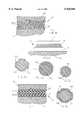
- FIG. 2represents a thick-film hybrid circuit structure 10 in which a conductor 18 is formed on an alumina substrate 12, and a circuit component 14 is electrically and mechanically connected to the conductor 18 with solder 16.
- High-conductivity thick-film conductors of the type represented in FIG. 2are typically formed from a paste containing a metal powder composed of silver, silver and palladium, a silver-palladium alloy, or admixtures of other metal powders.
- the pastetypically contains glass and/or metal oxide particles as inorganic binders, and an organic vehicle system that serves as a binder for the paste.
- the conductor pasteis deposited on the alumina substrate 12 and fired, such that the organic binder is removed and the powder particles and inorganic binders fuse to form the solid conductor 18.
- the solder 16 used to secure a circuit component 14 to the conductor 18is typically a tin-lead composition, frequently near the eutectic composition, with relatively high tin content to allow for lower processing temperatures.
- FIG. 1represents a cross-sectional view through a prior art conductor 20, which is depicted as being composed of metal particles 22 in direct contact with each other and the solder 16 (for simplicity and clarity, inorganic binder particles are not shown).
- the operability of the hybrid circuit 10 depicted in FIG. 2requires that the bond between the conductor 18 and solder 16 survive numerous thermal cycles, necessitating that the conductor 18 exhibit adequate solderability such that solder initially wets the conductor surface, and that adhesion between the conductor 18 and solder 16 is suitably maintained over an extended period of time.
- the conductor 18 and solder 16exhibit adequate solderability such that solder initially wets the conductor surface, and that adhesion between the conductor 18 and solder 16 is suitably maintained over an extended period of time.
- interactions that occur between the conductor 18 and solder 16can ultimately lead to degradation of the mechanical integrity of the assembly. It is generally recognized that when a silver-based conductor is soldered with a tin-lead solder, a brittle intermetallic region is formed between the conductor 18 and solder 16 during soldering, and may subsequently increase in thickness during high temperature exposure.
- the intermetallic regionis generally the weak mechanical link of the conductor-solder bond, and is particularly prone to fracturing during thermal cycling due to the differing coefficients of thermal expansion of the intermetallic and the conductor and solder materials, which induces significant stresses at the interface between these structures.
- Solderssuch as tin-lead solders, that exhibit high solderability on thick film conductors tend to promote the formation of this intermetallic region at the conductor-solder interface with metallic conductors.
- Such soldersgenerally have a greater tendency to leach elemental metal from the conductor 18 during soldering, and promote diffusion of tin from the solder 16 into the conductor 18 during high-temperature exposure.
- the growth of the intermetallic regionis limited by the relatively low service temperature of the circuit 10.
- the size of the intermetallic regionincreases significantly, which generally exacerbates the detrimental effect that the intermetallic region has on the service life of the circuit structure.
- the leach resistance of a metallic thick-film conductorcould be increased, and its resistance to diffusion of tin increased, so as to minimize the size of the intermetallic region that forms between the conductor and tin-lead solders at elevated temperatures. In doing so, it would be necessary to maintain the wettability and electrical conductivity of the conductor.
- approaches to date to improve leach resistance and tin-diffusion resistancehave included increasing the palladium content and the glass content of the films, both of which have had the undesirable effect of increasing the resistance of the conductor.
- the present inventionis directed to an improved thick film circuit including a conductor composition printed, dried and fired on a substrate to form a thick-film conductor, and a circuit component connected to the conductor with a tin-based solder, the conductor composition comprising metallic particles selected from the group of silver, palladium, platinum, copper and gold particles; and an inorganic coating on the surface of each of the particles, selected from the group of materials that are both (a) substantially inert at the firing temperature; and (b) non-wettable by the tin-based solder.
- the coatingserves to limit leaching of the conductor's elemental metal into the solder during soldering and diffusion of the solder's elemental tin into the conductor during subsequent high temperature operation of the circuit, thereby limiting the formation of an intermetallic region between the conductor and the solder. Since the extent of the intermetallic region is reduced, the conductor-solder bond is highly resistant to thermal cycle fatigue.
- the coatingmay be continuous or discontinuous, and may be applied to some or all of the particles of the conductor paste.
- a discontinuous coatingresults in portions of the surface of each particle being un-coated, so as to promote electrical contact between adjacent particles.
- FIG. 1is a cross-sectional representation of a conductor formed from a thick-film conductor paste of the prior art
- FIG. 2shows, in cross-section, a portion of a thick-film hybrid circuit having a circuit component mounted with solder to a thick-film conductor in accordance with this invention
- FIGS. 3a through 3dare cross-sectional representations of metallic particles for conductor pastes in accordance with different embodiments of this invention.
- FIG. 4is a cross-sectional representation of a conductor formed from a thick-film conductor paste in accordance with an embodiment of this invention.
- FIG. 4Portrayed in FIG. 4 is a conductor 120 formed by a conductor paste in accordance with this invention.
- the conductor 120is shown as being disposed between a substrate 12 and solder 16, the latter of which serves to bond a component 14 (not shown) to the conductor 120, similar to that illustrated in FIG. 2.
- the substrate 12is formed from an insulating material, such as alumina, as is conventional in the fabrication of hybrid circuits of the type represented in FIG. 2.
- substrate 12can be aluminum nitride, a glass-ceramic, insulated metal, or a layer of un-fired tape in a laminate structure.
- the solder 16can be a tin-lead composition, of which various formulations are commercially available.
- the conductor 120is formed from a conductor paste composed of a metallic powder, each particle 122 of which has an inorganic cladding layer 124.
- the conductor paste that forms the conductor 120would include an organic vehicle system (not shown) interspersed throughout the metallic powder in order to temporarily bind the particles 122 together and enable deposition of the conductor paste by any suitable printing technique, and would further include an inorganic binder (not shown) that fuses the particles 122 together during firing.
- the organic and inorganic bindersare not illustrated in the Figures in order to simplify the illustrations.
- the particles 122can be formed from any material that will adequately conduct electricity, such as silver, palladium, platinum, copper, gold and mixtures and alloys thereof.
- the cladding layer 124does not fully encapsulate each particle 122, but instead is discontinuous such that some regions of the surface of each particle 122 remain unclad. This aspect of the invention allows each particle 122 to electrically contact adjacent particles 122 through the unclad surface regions.
- the material for the cladding layer 124is solder resistant, and is inert in the sense that it does not alloy with the particles 122 or otherwise directly modify the composition of the particles 122 at thick film firing temperatures.
- Preferred cladding materialsare particularly capable of forming a barrier layer that inhibits leaching of metal from the conductor 120 and diffusion of metal from the solder 16.
- the cladding layer 124may comprise glass or refractory compounds such as oxides, silicides and/or nitrides of aluminum, zirconium, beryllium, tungsten, magnesium, calcium, niobium, titanium and zinc, and oxides and/or nitrides of silicon for firing temperatures of 850-100 degrees C. At lower firing temperatures, such as between 500-700 degrees C., other compounds such as oxides of copper, nickel, rhodium and molybdenum would also remain inert, and thus also reduce leaching and diffusion.
- glass or refractory compoundssuch as oxides, silicides and/or nitrides of aluminum, zirconium, beryllium, tungsten, magnesium, calcium, niobium, titanium and zinc, and oxides and/or nitrides of silicon for firing temperatures of 850-100 degrees C. At lower firing temperatures, such as between 500-700 degrees C., other compounds such as oxides of copper, nickel, rhodium and
- An alternate to the embodiment shown in FIG. 4is to intermix the clad particles 122 shown in FIG. 3a with unclad particles of the same or different composition.
- this approach to the inventionpromotes the conductivity of the conductor 120 while still enhancing resistance to leaching and diffusion.
- the ratio of clad particles 122 to unclad particlescan be varied to achieve an optimum balance between solderability and resistance to diffusion for a particular application.
- metal particles 122are provided with a continuous cladding layer 124a, over which a metallic coating 126 is deposited.
- the metallic coating 126is a conductive material, and preferably a metal such as silver, palladium, platinum, copper, gold and mixtures and alloys thereof.
- the combination of the metal particles 122 and the coating 126promotes the conductivity of the conductor 120, while the cladding layer 124a again serves to inhibit diffusion of tin from the solder 16 into the conductor 120.
- 3c and 3dillustrate further embodiments in which a continuous cladding layer 124a is employed without a metallic coating 126, and a discontinuous cladding layer 124 is employed with a continuous metallic coating 126, respectively. It should be noted that, to achieve acceptable electrical conductivity, the embodiment shown in FIG. 3c would be combined with unclad particles and/or a powder composed of any one or more of those particles depicted in FIGS. 3a, 3b and/or 3d.
- LTCCLow-Temperature Co-fired Ceramic
- the present inventioncan be used to make thick-film conductors for this type of process by selecting coating compounds that are chemically inert at these processing temperatures.
- all the aforementioned advantagescan be realized for the top printed layer or if any soldering occurs on the inner layers, with an opening on the upper layers.
- the top conductor layeris printed and fired separately much like on an alumina substrate. In this approach also, the current invention finds application and utility.
- thick-film conductors of the type represented in FIG. 4find use in thick-film hybrid circuits of the type shown in FIG. 2.
- the advantages of this inventionare evident when applied to essentially any thick-film hybrid circuit, including those hybrid circuits exposed to high temperatures over extended periods of time, during which tin tends to diffuse from the solder 16 into the conductor 18, and the intermetallic region between the solder 16 and conductor 18 tends to grow appreciably.
- a key aspect of this inventionis that the cladding layers 124 and 124a inhibit the leaching of elemental metal from the particles 122 during the soldering operation and the diffusion of tin from the solder 16 into the conductor 18 during subsequent high temperature excursions, thereby significantly promoting the conductor-solder bond strength and inhibiting the formation of the undesirable intermetallic region.
- the adhesion characteristics of the conductor 18 and solder 16are significantly promoted, and the service-life of a thick-film hybrid circuit utilizing this invention is substantially lengthened.
- the cladding materials evaluatedwere alumina and zirconia applied at one of two approximate quantity levels, measured as cladding oxide content in parts per million (ppm).
- the thicknesses noted in Table Iwere calculated on the presumption that the coatings were continuous, but have values of less than the dimension of a single atom or molecule. Therefore, it was concluded that the coatings were not continuous, but instead were discontinuous.
- the clad silver powders (E-H)were evaluated alone, admixed with the clad palladium powders (A-D) at a ratio of 3:1, and admixed with unclad palladium powders at a ratio of 3:1, as indicated in Table II below.
- conductors formed from unclad silver and palladium powderswere also evaluated. Each powder mixture was combined with suitable inorganic additives and an organic binder, printed on an alumina substrate, and then fired at conventional temperatures to form a thick-film conductor.
- Sheet resistances of the resulting conductorswere measured using a serpentine pattern typically used for that purpose. Measured sheet resistance of the thick-film conductors ranged from about 15 to about 23 milliohms/square for the 3Ag:1Pd conductors and about 1.7 to about 2.5 milliohms/square for the pure silver conductors. These ranges correspond to the resistance of conductors made utilizing prior art conductor pastes.
- Table IIsummarizes the solderability and adhesion strength characteristics of the thick-film conductors formed from the tested powder mixtures. Solderability of the conductors with 60Sn/40Pb solder was evaluated via a wetting test in which alumina substrates covered with conductor material were immersed in molten solder and the wetting force applied by the solder was measured. The adhesion strengths of the conductor/solder combinations were determined by using a wire lead peel test. Peel test samples were fabricated by dip-soldering tinned copper wires to pads of conductor material. Wire leads were forcibly removed and the force required to do so was recorded after intervals of 24 and 48 hours at 170° C.
- the results tabulated in Table IIindicated that the presence of cladding reduced the initial wetting capacity of the solder.
- the composition of the claddinghad a marked effect on the solderability of the pure silver conductors.
- zirconia cladding on pure silver powdershad only a nominal effect on solderability, while alumina cladding had a relatively greater effect on the solderability of conductors made from those same powders.
- Leach resistancewas inferred by dipping samples printed with a serpentine pattern of conductor material into molten 60Sn/40Pb solder. The resistance of the serpentine pattern was measured initially and after each dip. The number of dips required to reach a resistance of greater than 30 MW was recorded as an indication of leach resistance for the pattern in the experimental set-up used.
- the leach resistance of conductors formed from the "E,” “G” and “H” clad silver powdersexhibited a significant increase in leach resistance as compared to conductors formed from an unclad pure silver powder, as evidenced by the number of times the conductor could be dipped into the molten solder before infinite resistance resulted.
Landscapes
- Chemical & Material Sciences (AREA)
- Engineering & Computer Science (AREA)
- Microelectronics & Electronic Packaging (AREA)
- Chemical Kinetics & Catalysis (AREA)
- Materials Engineering (AREA)
- Mechanical Engineering (AREA)
- Metallurgy (AREA)
- Organic Chemistry (AREA)
- Dispersion Chemistry (AREA)
- Condensed Matter Physics & Semiconductors (AREA)
- Computer Hardware Design (AREA)
- General Physics & Mathematics (AREA)
- Power Engineering (AREA)
- Physics & Mathematics (AREA)
- Inorganic Chemistry (AREA)
- Parts Printed On Printed Circuit Boards (AREA)
Abstract
Description
TABLE I______________________________________ Cladding Cladding Powder Cladding Quantity Thickness*Powder Metal Material (ppm) (Angstroms)______________________________________A Pd ZrO.sub.2 480 0.47B Pd ZrO.sub.2 1585 1.47C Pd Al.sub.2 O.sub.3 481 1.03D Pd Al.sub.2 O.sub.3 1462 1.43E Ag ZrO.sub.2 480 1.05F Ag ZrO.sub.2 1150 1.51G Ag Al.sub.2 O.sub.3 510 1.01H Ag Al.sub.2 O.sub.3 1380 2.23______________________________________ *Values calculated assuming spherical particles and uniform, continuous cladding thickness.
TABLE II______________________________________ Wetting Adhesion Strength (N)Powder Force.sup.1 After Aging at 170° C.Mixture (mN) 0 hrs. 24 hrs. 48 hrs.______________________________________3Ag:1Pd Metallic Powder Conductorsunclad 10.54 22.5 15.3 13.8A + E 6.65 19.0 12.4 11.6B + F 4.86 19.8 14.4 16.3C + G 5.37 21.2 15.9 16.4D + H 6.49 18.6 9.6 13.6H + Pd.sup.2 7.36 24.4 21.0 20.1Ag Metallic Powder Conductorsunclad 14.63 17.8 0 0E 14.41 18.4 0 0F 11.32 13.8 0 0G 7.91 12.8 6.8 5.9H 4.53 7.2 0 0______________________________________ Note 1: Measured using a standard pattern with a Multicore Solderability Tester, manufactured by Multicore, Hemel Hempstead, Herts, U.K. Note 2: Unclad palladium powder.
Claims (10)
Priority Applications (1)
| Application Number | Priority Date | Filing Date | Title |
|---|---|---|---|
| US08/954,385US5928568A (en) | 1996-06-24 | 1997-10-20 | Thick film circuit having conductor composition with coated metallic particles |
Applications Claiming Priority (2)
| Application Number | Priority Date | Filing Date | Title |
|---|---|---|---|
| US08/668,900US5716552A (en) | 1996-06-24 | 1996-06-24 | Thick-film conductor compostions comprising silver or palladium particles coated with alumina or zirconia |
| US08/954,385US5928568A (en) | 1996-06-24 | 1997-10-20 | Thick film circuit having conductor composition with coated metallic particles |
Related Parent Applications (1)
| Application Number | Title | Priority Date | Filing Date |
|---|---|---|---|
| US08/668,900Continuation-In-PartUS5716552A (en) | 1996-06-24 | 1996-06-24 | Thick-film conductor compostions comprising silver or palladium particles coated with alumina or zirconia |
Publications (1)
| Publication Number | Publication Date |
|---|---|
| US5928568Atrue US5928568A (en) | 1999-07-27 |
Family
ID=46253761
Family Applications (1)
| Application Number | Title | Priority Date | Filing Date |
|---|---|---|---|
| US08/954,385Expired - LifetimeUS5928568A (en) | 1996-06-24 | 1997-10-20 | Thick film circuit having conductor composition with coated metallic particles |
Country Status (1)
| Country | Link |
|---|---|
| US (1) | US5928568A (en) |
Cited By (9)
| Publication number | Priority date | Publication date | Assignee | Title |
|---|---|---|---|---|
| US6368378B2 (en)* | 1999-12-22 | 2002-04-09 | Mitsui Mining And Smelting Co., Ltd. | Paste to be fired for forming circuit board and method for preparing surface-modified silver powder |
| US6476332B1 (en) | 2001-09-12 | 2002-11-05 | Visteon Global Technologies, Inc. | Conductor systems for thick film electronic circuits |
| US20030006787A1 (en)* | 2000-06-28 | 2003-01-09 | Toshio Kazama | Conductive contact |
| EP1402989A1 (en)* | 2002-09-23 | 2004-03-31 | Delphi Technologies, Inc. | Leach-resistant solder alloys for silver-based thick-film conductors |
| US20050104046A1 (en)* | 2003-11-19 | 2005-05-19 | Yueli Wang | Thick film conductor case compositions for LTCC tape |
| US20080029202A1 (en)* | 2004-10-19 | 2008-02-07 | E.I. Du Pont De Nemours | Thick film conductor case compositions for ltcc tape |
| US7754976B2 (en) | 2002-04-15 | 2010-07-13 | Hamilton Sundstrand Corporation | Compact circuit carrier package |
| US20110155430A1 (en)* | 2009-12-24 | 2011-06-30 | Gyu Ho Lee | Anisotropic conductive adhesive composite and film, and circuit connecting structure including the same |
| US20150027524A1 (en)* | 2011-09-09 | 2015-01-29 | Heraeus Precious Metals North America Conshohocken Llc | Silver solar cell contacts |
Citations (9)
| Publication number | Priority date | Publication date | Assignee | Title |
|---|---|---|---|---|
| US4493789A (en)* | 1980-03-31 | 1985-01-15 | Hitachi Chemical Company, Ltd. | Electroconductive paste and process for producing electroconductive metallized ceramics using the same |
| US4521329A (en)* | 1983-06-20 | 1985-06-04 | E. I. Du Pont De Nemours And Company | Copper conductor compositions |
| US4906404A (en)* | 1988-11-07 | 1990-03-06 | Dai-Ichi Kogyo Seiyaku Co., Ltd. | Copper conductor composition |
| US5207950A (en)* | 1989-03-16 | 1993-05-04 | Ercon, Inc. | Polymer composition containing chlorided conductive particles |
| US5294374A (en)* | 1992-03-20 | 1994-03-15 | Leviton Manufacturing Co., Inc. | Electrical overstress materials and method of manufacture |
| US5415944A (en)* | 1994-05-02 | 1995-05-16 | Motorola, Inc. | Solder clad substrate |
| US5453293A (en)* | 1991-07-17 | 1995-09-26 | Beane; Alan F. | Methods of manufacturing coated particles having desired values of intrinsic properties and methods of applying the coated particles to objects |
| US5716663A (en)* | 1990-02-09 | 1998-02-10 | Toranaga Technologies | Multilayer printed circuit |
| US5737191A (en)* | 1995-04-07 | 1998-04-07 | Shinko Electric Industries Co., Ltd. | Structure and process for mounting semiconductor chip |
- 1997
- 1997-10-20USUS08/954,385patent/US5928568A/ennot_activeExpired - Lifetime
Patent Citations (9)
| Publication number | Priority date | Publication date | Assignee | Title |
|---|---|---|---|---|
| US4493789A (en)* | 1980-03-31 | 1985-01-15 | Hitachi Chemical Company, Ltd. | Electroconductive paste and process for producing electroconductive metallized ceramics using the same |
| US4521329A (en)* | 1983-06-20 | 1985-06-04 | E. I. Du Pont De Nemours And Company | Copper conductor compositions |
| US4906404A (en)* | 1988-11-07 | 1990-03-06 | Dai-Ichi Kogyo Seiyaku Co., Ltd. | Copper conductor composition |
| US5207950A (en)* | 1989-03-16 | 1993-05-04 | Ercon, Inc. | Polymer composition containing chlorided conductive particles |
| US5716663A (en)* | 1990-02-09 | 1998-02-10 | Toranaga Technologies | Multilayer printed circuit |
| US5453293A (en)* | 1991-07-17 | 1995-09-26 | Beane; Alan F. | Methods of manufacturing coated particles having desired values of intrinsic properties and methods of applying the coated particles to objects |
| US5294374A (en)* | 1992-03-20 | 1994-03-15 | Leviton Manufacturing Co., Inc. | Electrical overstress materials and method of manufacture |
| US5415944A (en)* | 1994-05-02 | 1995-05-16 | Motorola, Inc. | Solder clad substrate |
| US5737191A (en)* | 1995-04-07 | 1998-04-07 | Shinko Electric Industries Co., Ltd. | Structure and process for mounting semiconductor chip |
Cited By (15)
| Publication number | Priority date | Publication date | Assignee | Title |
|---|---|---|---|---|
| US6368378B2 (en)* | 1999-12-22 | 2002-04-09 | Mitsui Mining And Smelting Co., Ltd. | Paste to be fired for forming circuit board and method for preparing surface-modified silver powder |
| US20030006787A1 (en)* | 2000-06-28 | 2003-01-09 | Toshio Kazama | Conductive contact |
| US6476332B1 (en) | 2001-09-12 | 2002-11-05 | Visteon Global Technologies, Inc. | Conductor systems for thick film electronic circuits |
| US7754976B2 (en) | 2002-04-15 | 2010-07-13 | Hamilton Sundstrand Corporation | Compact circuit carrier package |
| EP1402989A1 (en)* | 2002-09-23 | 2004-03-31 | Delphi Technologies, Inc. | Leach-resistant solder alloys for silver-based thick-film conductors |
| US7261841B2 (en) | 2003-11-19 | 2007-08-28 | E. I. Du Pont De Nemours And Company | Thick film conductor case compositions for LTCC tape |
| US20050106369A1 (en)* | 2003-11-19 | 2005-05-19 | Yueli Wang | Thick film conductor case compositions for LTCC tape |
| US7303698B2 (en) | 2003-11-19 | 2007-12-04 | E.I. Du Pont De Nemours And Company | Thick film conductor case compositions for LTCC tape |
| US20050104046A1 (en)* | 2003-11-19 | 2005-05-19 | Yueli Wang | Thick film conductor case compositions for LTCC tape |
| US20080029202A1 (en)* | 2004-10-19 | 2008-02-07 | E.I. Du Pont De Nemours | Thick film conductor case compositions for ltcc tape |
| US7731812B2 (en) | 2004-10-19 | 2010-06-08 | E.I. Du Pont De Nemours And Company | Thick film conductor case compositions for LTCC tape |
| US20110155430A1 (en)* | 2009-12-24 | 2011-06-30 | Gyu Ho Lee | Anisotropic conductive adhesive composite and film, and circuit connecting structure including the same |
| US9035192B2 (en)* | 2009-12-24 | 2015-05-19 | Cheil Industries, Inc. | Anisotropic conductive adhesive composite and film, and circuit connecting structure including the same |
| US20150027524A1 (en)* | 2011-09-09 | 2015-01-29 | Heraeus Precious Metals North America Conshohocken Llc | Silver solar cell contacts |
| US10038109B2 (en)* | 2011-09-09 | 2018-07-31 | Heraeus Precious Metals North America Conshohocken Llc | Silver solar cell contacts |
Similar Documents
| Publication | Publication Date | Title |
|---|---|---|
| KR100309229B1 (en) | Lead-free solder and soldered article | |
| JP3575311B2 (en) | Pb-free solder and soldering article | |
| US5627344A (en) | Multilayer ceramic circuit substrate, process for producing the same, and electrically conductive material for use in multilayer ceramic circuit substrate | |
| US5928568A (en) | Thick film circuit having conductor composition with coated metallic particles | |
| US5716552A (en) | Thick-film conductor compostions comprising silver or palladium particles coated with alumina or zirconia | |
| US7173510B2 (en) | Thermal fuse and method of manufacturing fuse | |
| JPH0957487A (en) | Brazing material | |
| JP4081865B2 (en) | Method for producing conductor composition | |
| JPS6342879B2 (en) | ||
| JPH08306816A (en) | Electrode pad | |
| JP2973558B2 (en) | Conductive paste for chip-type electronic components | |
| JP2627509B2 (en) | Electronic component having conductive layer | |
| JP2631010B2 (en) | Thick film copper paste | |
| JP3792642B2 (en) | Wiring board and manufacturing method thereof | |
| JPS63283184A (en) | Circuit substrate covered with conductor composition | |
| JP2000223821A (en) | Ceramic wiring board | |
| JPH10193170A (en) | Soldered article | |
| JP3556377B2 (en) | Wiring board | |
| JPH06302927A (en) | Ceramic wiring board, its manufacture and electrode paste | |
| JP2006203230A (en) | WIRING BOARD AND ELECTRONIC DEVICE USING THE SAME | |
| JP3857219B2 (en) | Wiring board and manufacturing method thereof | |
| JPS6318357B2 (en) | ||
| JP2614147B2 (en) | Organometallic conductor composition | |
| JPH0521935A (en) | Circuit board | |
| JP2892220B2 (en) | Manufacturing method of ceramic wiring board |
Legal Events
| Date | Code | Title | Description |
|---|---|---|---|
| AS | Assignment | Owner name:DELCO ELECTRONICS CORPORATION, INDIANA Free format text:ASSIGNMENT OF ASSIGNORS INTEREST;ASSIGNORS:PASZKIET, CHRISTINE ANN;SARMA, DWADASI HARE RAMA;REEL/FRAME:008904/0871;SIGNING DATES FROM 19971015 TO 19971016 | |
| STCF | Information on status: patent grant | Free format text:PATENTED CASE | |
| FPAY | Fee payment | Year of fee payment:4 | |
| AS | Assignment | Owner name:DELPHI TECHNOLOGIES, INC., MICHIGAN Free format text:ASSIGNMENT OF ASSIGNORS INTEREST;ASSIGNOR:DELCO ELECTRONICS CORPORATION;REEL/FRAME:016700/0623 Effective date:20050701 | |
| AS | Assignment | Owner name:JPMORGAN CHASE BANK, N.A., TEXAS Free format text:SECURITY AGREEMENT;ASSIGNOR:DELPHI TECHNOLOGIES, INC.;REEL/FRAME:016237/0402 Effective date:20050614 | |
| FPAY | Fee payment | Year of fee payment:8 | |
| AS | Assignment | Owner name:DELPHI TECHNOLOGIES, INC., MICHIGAN Free format text:RELEASE OF SECURITY AGREEMENT;ASSIGNOR:JPMORGAN CHASE BANK, N.A.;REEL/FRAME:020808/0583 Effective date:20080225 | |
| FEPP | Fee payment procedure | Free format text:PAYOR NUMBER ASSIGNED (ORIGINAL EVENT CODE: ASPN); ENTITY STATUS OF PATENT OWNER: LARGE ENTITY | |
| AS | Assignment | Owner name:DELPHI TECHNOLOGIES, INC., MICHIGAN Free format text:CHAIN OF TITLE;ASSIGNOR:DELPHI TECHNOLOGIES, INC.;REEL/FRAME:022552/0482 Effective date:20090416 | |
| AS | Assignment | Owner name:CASANTRA ACQUISTION III LLC, DELAWARE Free format text:ASSIGNMENT OF ASSIGNORS INTEREST;ASSIGNOR:DELPHI TECHNOLOGIES, INC.;REEL/FRAME:023015/0720 Effective date:20090515 | |
| AS | Assignment | Owner name:CASANTRA ACQUISITION III LLC, DELAWARE Free format text:CORRECTIVE ASSIGNMENT TO CORRECT THE ASSIGNEE NAME PREVIOUSLY RECORDED ON REEL 023015 FRAME 0720;ASSIGNOR:DELPHI TECHNOLOGIES, INC.;REEL/FRAME:023107/0581 Effective date:20090515 | |
| FPAY | Fee payment | Year of fee payment:12 | |
| FEPP | Fee payment procedure | Free format text:PAYER NUMBER DE-ASSIGNED (ORIGINAL EVENT CODE: RMPN); ENTITY STATUS OF PATENT OWNER: LARGE ENTITY Free format text:PAYOR NUMBER ASSIGNED (ORIGINAL EVENT CODE: ASPN); ENTITY STATUS OF PATENT OWNER: LARGE ENTITY | |
| AS | Assignment | Owner name:CALLAHAN CELLULAR L.L.C., DELAWARE Free format text:MERGER;ASSIGNOR:CASANTRA ACQUISITION III LLC;REEL/FRAME:037520/0962 Effective date:20150826 |