US5926838A - Interface for high speed memory - Google Patents
Interface for high speed memoryDownload PDFInfo
- Publication number
- US5926838A US5926838AUS08/820,595US82059597AUS5926838AUS 5926838 AUS5926838 AUS 5926838AUS 82059597 AUS82059597 AUS 82059597AUS 5926838 AUS5926838 AUS 5926838A
- Authority
- US
- United States
- Prior art keywords
- circuit
- memory device
- data
- read
- signal
- Prior art date
- Legal status (The legal status is an assumption and is not a legal conclusion. Google has not performed a legal analysis and makes no representation as to the accuracy of the status listed.)
- Expired - Lifetime
Links
Images


Classifications
- G—PHYSICS
- G06—COMPUTING OR CALCULATING; COUNTING
- G06F—ELECTRIC DIGITAL DATA PROCESSING
- G06F13/00—Interconnection of, or transfer of information or other signals between, memories, input/output devices or central processing units
- G06F13/14—Handling requests for interconnection or transfer
- G06F13/16—Handling requests for interconnection or transfer for access to memory bus
- G06F13/1668—Details of memory controller
- G06F13/1689—Synchronisation and timing concerns
- G—PHYSICS
- G11—INFORMATION STORAGE
- G11C—STATIC STORES
- G11C7/00—Arrangements for writing information into, or reading information out from, a digital store
- G11C7/10—Input/output [I/O] data interface arrangements, e.g. I/O data control circuits, I/O data buffers
- G11C7/1072—Input/output [I/O] data interface arrangements, e.g. I/O data control circuits, I/O data buffers for memories with random access ports synchronised on clock signal pulse trains, e.g. synchronous memories, self timed memories
- G—PHYSICS
- G11—INFORMATION STORAGE
- G11C—STATIC STORES
- G11C7/00—Arrangements for writing information into, or reading information out from, a digital store
- G11C7/22—Read-write [R-W] timing or clocking circuits; Read-write [R-W] control signal generators or management
Definitions
- the present inventionrelates to memory interface circuits and methods, and more particularly, to memory interfaces for high speed memory such as burst EDO and synchronous memory devices.
- the memory devicestypically include a dynamic random access memory (DRAM) packaged as a module, such as a single in-line memory module (SIMM) or a dual in-line memory module (DIMM).
- DRAMdynamic random access memory
- the memory moduletypically includes one or more banks of memory chips connected in parallel such that each memory bank stores one set of data, such as a word or double word, per memory address.
- the memory controllercommunicates with, and interprets commands from, the CPU. For example, the CPU issues a command and an address which are received and translated by the memory controller. The memory controller, in turn, applies appropriate command signals and row and column addresses to the memory device. Examples of such commands include a row address strobe (RAS), column address strobe (CAS), write enable (WE), and possibly a clock signal (CLK). (The line or bar over the acronym for a symbol generally indicates that the active state for the particular signal is a logical low value.) In response to the commands and addresses, data is transferred between the CPU and the memory device.
- RASrow address strobe
- CAScolumn address strobe
- WEwrite enable
- CLKclock signal
- the speed of memory deviceshas not been able to keep pace with the speed advances in current CPUs.
- the speed of current computer systemsis limited by the speed in which data and instructions can be accessed from the memory devices of the computer system.
- each memory chiptypically includes only enough address terminals to specify either the row address or the column address but not both simultaneously.
- the typical memory controlleraccesses a memory location sequentially by first transmitting the row address and then transmitting the column address. Specifically, the memory controller provides the row address to the memory device, asserts the RAS control signal, then provides the column address on the memory device and asserts the CAS control signal. To ensure proper timing, the memory controller provides a brief delay after asserting the RAS control signal and before asserting the CAS signal (RAS/CAS delay).
- the FPM DRAMeliminates the RAS/CAS delay when successive accesses to the same row of memory occur. Because the majority of program execution is sequential in nature, program execution very often proceeds along a row of memory.
- the memory controllercompares the row address of the memory location currently being accessed with the row address for the next memory access. If the row addresses are the same (known as a "page hit"), then the memory controller continues asserting the RAS control signal at the end of a current bus cycle. Because the memory already has the correct row address, the new column address can be immediately transferred to the memory without requiring a RASCAS delay.
- Extended data out (EDO) DRAMsimprove upon the FPM DRAMs.
- the CAS high-to-low transitionlatches the column address, while the CAS low-to-high transition turns off an output buffer of the DRAM.
- EDO DRAMsinstead separate the two functions of the CAS signal. The low-to-high transition of CAS no longer turns off the output buffer. This change provides an extended time during which the output data is valid, hence the "extended data out" name.
- EDO memoryallows the CPU to sample the output data even while an address for a subsequent data transfer operation is being set up for the next read cycle.
- BEDO DRAMsBurst EDO (BEDO) DRAMs improve upon the good idea used in EDO DRAMs (leaving data valid even after CAS goes high).
- Most current CPUstypically access BEDO DRAMs in four-cycle bursts at four adjacent memory locations to fill a cache memory. Recognizing this typical access operation, BEDO DRAMs quickly provide the following three addresses itself after receiving the first address.
- BEDO DRAMstypically include a two-bit counter which provides three column addresses after the first received column address. The memory controller, and CPU, thus avoid the tight timing requirements of providing multiple addresses at appropriate times to the DRAM device.
- BEDO DRAMscan provide bursting at rates of up to 5-1-1-1 or less.
- DRAMsynchronous DRAM
- FPM, EDO, and BEDO DRAMare asynchronous DRAM devices because they do not require a clock input signal.
- the memory controller for asynchronous devicesreceives the system clock signal and operates as a synchronous interface with the CPU so that data is exchanged with the CPU at appropriate edges of the clock signal.
- Memory controllers for SDRAM devicesare necessarily simpler because the SDRAM devices and the CPU both operate based on a clock signal. To achieve optimum performance with a CPU, the SDRAM device must be synchronized with the CPU.
- both BEDO DRAM and SDRAM devicesrequire comparatively strict timing requirements compared to FPM and EDO DRAM devices.
- the strict timing requirements of BEDO DRAMrequires a strict relation between generating an edge of CAS and when data is valid for reading or writing to the memory device. During each read cycle, CAS must fall during the middle of the period when data is to be read from the BEDO DRAM. For example, there is very little room for time delay or skew between the system clock and the CAS control signal supplied to the BEDO DRAM when the BEDO DRAM is operated in the 5-1-1-1 burst mode.
- BEDO memory devicesThe slow acceptance of BEDO memory devices is partially due to the strict timing requirements needed to run the devices in 1,1,1 burst mode. There is very little room for skew between the system clock and the CAS control signal. The read and write requirements for the devices are also at odds with each other. For synchronous ("Sync") DRAM devices, performance is limited by clock skew within the system as seen by the memory devices and the memory controller. Once again, read and write requirements are conflicting.
- Syncsynchronous
- Embodiments of the present inventionprovide a simple, robust method for a memory controller device or other device to interface to BEDO or Sync DRAM memory. Separate read and write control is provided.
- an embodiment of the present inventionapplies a programmable delay to a copy of the CAS signal as seen by the BEDO device, which is used to control two or more read latches.
- the read latchesare then multiplexed, in alternating fashion, to a read register, and clocked by the system clock. This allows for a 2 clock crossing between the clock that produced the CAS signal and the register that clocks read data. This method provides plenty of margin for bursted reads.
- BEDO writeson the other hand, have different setup and hold requirements.
- An embodiment of the present inventioncreates a CAS signal delayed from the clock used to send write data.
- the CAS signalis delayed to center the falling edge with valid write data.
- Datais sent to the BEDO device from a register clocked by the positive edge system clock. This allows data to arrive before the falling edge of the CAS signal and provides the necessary write data hold time.
- the edge that the CAS signal producedis programmable via a configuration register.
- the clock as seen by the memory deviceis delayed by a programmable delay under an embodiment of the present invention. This delay will account for memory output, board crossing and memory controller input delays. The delay will be configured by the system BIOS for a given board or system implementation.
- Sync DRAM writesare strobed by the negative edge of the clock that produced the Sync DRAM control and data under an embodiment of the present invention. The negative edge of the clock is aligned at the center of valid write data. In all cases, a programmable delay can be inserted to provide a flexible method for controlling read and write data.
- the present inventionis directed to an interface circuit and method, which can form part of a computer system, memory device, memory controller, etc.
- the interface circuitmay include a read circuit, a write circuit and a clocking circuit.
- the read circuitmay include two storage devices that alternatively receive data read from high speed memories such as BEDO and SDRAM devices.
- a multiplexer and read output registerprovide the read data to a CPU or other application. If the memory is burst EDO, then the clocking circuit in the examplary embodiment receives the system clock signal and generates a CAS signal based on positive or negative going edges of the clock signal, depending upon delays inherent in the system in which the present invention is employed.
- the CAS signalis also used to drive the two storage devices.
- the clock circuit in an exemplary embodimentincludes an inverter that inverts the clock signal, and provides the inverted clock signal to the SDRAM.
- the inverted clock signalis delayed and then used to drive the two storage devices.
- a write register in the write circuitis driven based on the system clock, and therefore operates separately from the read circuit, but which is synchronized with control of the memory device.
- the apparatus of the present inventioneffectively forms an interface between a CPU and/or memory controller circuit and a semiconductor memory device.
- the apparatusincludes a clock circuit, a read circuit and an optional write circuit.
- the clock circuitis coupled to the CPU and the memory device.
- the clock circuitreceives a timing signal and produces an interface clocking signal that is provided to the memory device.
- the read circuitis coupled to the memory device, the CPU and the clock circuit.
- the read circuithas first and second storage circuits that receive alternate data read from the memory device in response to portions of the interface clocking signal, and output the read data to the CPU.
- the write circuitis coupled to the memory device, the CPU and the clock circuit.
- the write circuitreceives write data from the CPU and provides the write data to the memory device.
- the write circuit datais written to the memory device in response to the interface clocking signal.
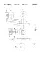
- FIG. 1is a block diagram of a computer system according to the present invention.
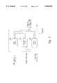
- FIG. 2is a block diagram of a memory interface of the computer system shown in FIG. 1.
- FIG. 3Ais a block diagram of a memory controller and BEDO memory, and signals exchanged therebetween, under embodiments of the present invention.
- FIG. 3Bis a block diagram of an exemplary embodiment of a read portion of the memory interface for use with BEDO DRAM devices.
- FIG. 3Cis a block diagram of an exemplary, alternative embodiment of the memory interface of FIGS. 3B and 3D.
- FIG. 3Dis a block diagram of an exemplary embodiment of a write portion of the memory interface for use with BEDO DRAM devices.
- FIG. 4is a timing diagram of a read operation performed by the memory interface and BEDO DRAM of FIG. 3.
- FIG. 5is a timing diagram of a write operation performed by the memory interface and BEDO DRAM of FIG. 3.
- FIG. 6Ais a block diagram of a memory controller and SDRAM memory, and signals exchanged therebetween, under embodiments of the present invention.
- FIG. 6Bis a block diagram of an exemplary embodiment of a read portion of the memory interface for use with SDRAM devices.
- FIG. 6Cis a block diagram of an exemplary embodiment of a write portion of the memory interface for use with SDRAM devices.
- FIG. 7is a timing diagram of a read operation performed by the memory interface and SDRAM of FIG. 6.
- FIG. 8is a timing diagram of a write operation performed by the memory interface and SDRAM of FIG. 6.
- An interface circuitand in particular, an interface circuit for use with high speed semiconductor memories such as BEDO or SDRAM, is described in detail herein.
- numerous specific detailsare set forth such as timing and execution of commands to the memory devices, components within the interface circuit, etc., in order to provide a thorough understanding of the present invention.
- One skilled in the relevant artwill readily recognize that the present invention can be practiced without use of certain specific details described herein, or with other specific timing, components, etc.
- Well-known structures and operationsare not shown or described in detail in order to avoid obscuring the present invention.
- a computer system 100such as an IBM compatible personal computer (“PC") includes a CPU or central processing unit (“CPU”) 102 coupled to a CPU bus 104.
- CPUcentral processing unit
- Examples of acceptable CPUsinclude Pentium®, Pentium® Pro, both manufactured by Intel Corporation, Alpha, manufactured by Digital Equipment Corporation, Power PC, manufactured by IBM, etc.
- a main memory array 106is coupled to the CPU bus 104 through a memory controller 108.
- the memory array 106can include SIMMs or DIMMs and may include any of various known BEDO DRAM and/or SDRAM devices, such as devices manufactured by Micron Technology, Inc.
- a system clock(not shown) provides a system clock signal to various components of the computer system 100, such as the CPU 102 and memory controller 108.
- An input/output (“I/O") bus 110is coupled to the CPU bus 104 through an I/O bridge controller 112.
- the I/O bridge controller 112monitors bus traffic on the CPU and I/O buses 104 and 110, and routes data therebetween when it detects appropriate transfer commands on either of the buses.
- the I/O bridge controller 112may also translate data between the buses, particularly when the CPU and I/O buses 104 and 110 have different widths and/or employ different formats, etc.
- One or more input devices 114such as a keyboard, mouse, etc., may also be coupled to the I/O bus 110.
- one or more output devices 116such as visual display devices, printers, etc., may be coupled to the I/O bus 110.
- one or more mass storage devices 118such as hard disk drives, CD-ROM drives, etc., may be coupled to the I/O bus 110.
- the memory interface 119can be formed as a separate device, or be incorporated or integrated with the memory controller 108, or with one or more memory devices in the memory array 106.
- the memory interface 119includes a read circuit 120 that reads data from the memory array 106, and provides such read data to the CPU 102. Conversely, a write circuit 122 receives write data from the CPU 102 and provides the write data to the memory array 106. A clocking circuit 124 receives a clock signal such as the system clock signal noted above. In one embodiment, the read and clocking circuits 120 and 124 can be employed without the write circuit 122.
- the memory interface 119 of FIG. 2receives a system clock signal from the memory controller 108, or alternatively directly from the system clock (not shown).
- the clocking circuit 124in response to the system clock signal, produces an interface clocking signal.
- BEDO DRAM or SDRAM devices in the memory array 106transfer data in response to the interface clocking signal.
- the clocking circuit 124produces a CAS signal as the interface clocking signal in response to the system clock signal input thereto.
- the clocking circuit 124produces an inverted clock signal as the interface clocking signal in response to the system clock signal input thereto. Producing an interface clocking signal reduces skew between the system clock and control signals, as discussed below.
- the read circuit 120includes at least two storage circuits, as described below, that receive alternate read data from the memory array 106 in response to alternating portions of the interface clocking signal from the clocking circuit 124.
- two storage circuitssuch as two read latches, two registers, or a single register of width sufficient to store two data groups that are read separately therefrom, the read circuit 120 ensures that one read latch is always ready to receive read data while the other is outputting previously read data.
- the read circuit 120can thus accommodate high speed memory in the memory array 106.
- the write circuit 122in one embodiment, includes a write data register that receives the write data from the CPU 102. The write data is clocked through the write register based on the clock signal. The write data, however, is written to the memory array 106 based not on the clock signal, but instead on the interface clocking signal. Such a difference between the clock signal and the interface clocking signal permits the interface circuit 119 to compensate for delays in the computer system 100, as described below.
- the memory controller 108includes the interface circuit 119 and provides the RAS, CAS, WE, and address signals to the BEDO memory in the memory array 106.
- the CAS signalis also fed back to the memory controller 108 as a read data strobe.
- FIG. 3Bshows first and second read latches 130 and 132 receive alternate read data from the BEDO memory in the memory array 106.
- an inverted copy of the CAS signalis used to control the read latches 130 and 132 during each read cycle.
- each data cyclewould include a falling edge of CAS when data is valid at an output of the EDO DRAM.
- BEDO DRAMoperating at high clock speeds
- timing of CAS with valid datais difficult.
- each read latchoperates at one-half speed, or every two CAS cycles.
- the two latchesoperate at a full speed rate of valid data read out during each CAS cycle.
- the read circuit 120provides for plenty of margin for time skew or delays in the system for bursted reads from the BEDO memory.
- a read multiplexer 134alternately receives the read data stored in the read latches 130 and 132.
- the read multiplexer 134is controlled by a signal that is in sync with the bursted data input to the read latches 130 and 132, so that the appropriate data stored in one latch is passed through the multiplexer, while the other read latch is receiving read data from the BEDO memory.
- the read multiplexer 134can include a counter which is synched with the system clock signal used to increment the burst counter of the BEDO memory.
- a read register 136receives the read data from the read multiplexer 134, and likewise outputs the read data in synchronism with the system clock signal.
- the clocking circuit 124may employ an inverter 145 which receives and inverts the CAS signal.
- a programmable delay element 143may be utilized to delay the inverted CAS signal and provide such delayed signal to clock the read latches 130 and 132.
- the programmable delay element 143provides a flexible method of controlling the output of data from the read latches 130 and 132. The amount of delay can be programmable by the user or by the BIOS instructions, depending upon loading or other delays in the computer system 100, as discussed herein.
- a first alternative embodiment of the interface circuit 119is shown as an interface circuit 119'.
- This and other alternative embodimentsare similar to the previously described embodiments, and all elements are similarly numbered when of similar construction. Only the significant differences in the construction or operation are discussed in detail.
- the interface circuit 119'provides an alternative clocking circuit 124.
- systems employing DRAMcan include long trace lengths on a given circuit board. Long trace lengths provide increased capacitive loading. In order to handle such increased loads, or when multiple types of memory devices are employed in a given system, buffers can be provided, which are external to the memory devices.
- the interface circuit 119may compensate for lightly loaded versus heavily loaded environments having short versus long delays, respectively.
- the clocking circuit 124generates the CAS signal for controlling the BEDO DRAM in synchronism with edges of, based on, the system clock signal.
- a CAS positive edge clock circuit 140receives the system clock signal, while an inverter 141 inverts the system clock signal and inputs the inverted system clock signal to a CAS negative edge clock circuit 142.
- the CAS positive clock and CAS negative clock circuits 140 and 142can include conventional programmable delay elements, pulse shaping circuits, or be omitted entirely, depending upon a given application for which the interface circuit 119 is adapted.
- a CAS multiplexer 144selects one of the output signals from the CAS positive clock and CAS negative clock circuits 140 and 142, and selectively outputs portions of one of these signals as the CAS signal.
- a Read signalprovided by the memory controller 108 to the CAS multiplexer 144, selects a particular edge of the system clock for the CAS signal. For example, during a read operation, the Read signal applied to the CAS multiplexer 144 selects positive going edges of the system clock signal to produce positive edges of CAS cycles (as shown in FIG. 4). As explained below, during a write operation, however, the Read signal selects negative going edges of the system clock signal to produce the CAS signal, after a delay that includes the delay caused by the inverter 141 (as shown as a delay 1 in the CAS signal in FIG. 5).
- the CAS signal output from the CAS multiplexer 144is provided to the BEDO memory of the memory array 106 to control conventional transfer of data to and from the memory.
- the inverted CAS signalis employed by the read latches 130 and 132 to produce appropriately timed Read Latch A and Read Latch B signals, respectively, for either memory controller 119 (FIG. 3B) or 119' (FIG. 3D).
- FIG. 4an exemplary timing diagram of a read operation is shown.
- the timing diagramincludes a system or CPU clock signal, the CAS signal, address signal ADDR, write enable signal WE, data read from the BEDO memory (BEDO DATA), latch enable signals (Read Latch 130 and Read Latch 132), data output from the read register 136 (Read Register) and data provided to the CPU (PROC DATA).
- the timing diagram of FIG. 4is generally self-explanatory to those skilled in the relevant art, as is the operation of BEDO DRAM.
- the CAS signalnot only controls the reading of data from the BEDO memory under standard BEDO operation, but also controls the latching of the read data into the read latches 130 and 132.
- control of the read latches 130 and 132are synchronized with the control of the BEDO memory, which thereby controls timing skew in the computer system 100.
- the CAS signalis synchronized with the system clock signal.
- a first group of data(BEDO DATA 0) is read from the BEDO memory and latched into the first read latch 130 upon the first rising edge of the Read Latch 130 signal.
- a third group of data(BEDO DATA 2) is read from the BEDO memory and latched into the first read latch 130 upon the next rising edge of the Read Latch 130 signal.
- the second read latch 132receives and latches the second and fourth groups of read data one clock or CAS cycle after the first and third cycles under the Read Latch 132 signal.
- a write register 150receives write data from the CPU 102 via the memory controller 108. The data is clocked out of the write register 150 in synchronism with the system clock signal which is input thereto.
- the clock circuit 124 of the memory controller 119creates a CAS signal delayed from the system clock signal to control the sending of write data to the BEDO memory.
- the created CAS signalmay be delayed by the clocking circuit 124 so that the falling edge of the signal is approximately centered with valid write data, as described herein, based on a positive edge of the system clock signal.
- dataarrives at the BEDO memory before the falling edge of the CAS signal, to thereby provide the necessary write data hold time.
- the clocking circuit 124produces an optimized CAS signal for the particular computer system 100 in which the BEDO memory is employed.
- a programmable configuration register (not shown) in the memory controller 108can be employed to determine whether the positive or negative going edges of the system clock signal are employed to initiate data transfer in the BEDO memory.
- Conventional memory controllersinclude configuration registers that are programmable by the basic input/output (BIOS) instructions of the computer system 100 whenever the computer system is initially energized.
- the BIOS instructionsmay program a configuration register in the memory controller 108 to provide one of two types of the Read signals. If the computer system is lightly loaded, then the memory controller 108 is programmed by the BIOS to provide a Read signal that instructs the CAS CAS multiplexer to pass the negative going edge of the system clock from the CAS negative clock circuit 142 as the positive going edge of each CAS cycle.
- the Read signalpasses the positive going edge of the system clock from the CAS positive clock circuit 140 as the positive going edge of each CAS cycle.
- the write circuit 122has sufficient time to write data to the BEDO memory in a heavily loaded system before the falling edge of CAS, to thereby provide the necessary hold time.
- the configuration registercan also identify BEDO memory in the memory array 106 if the memory array includes other types of memory devices having timing requirements which differ from the BEDO memory.
- the timing diagram of FIG. 5shows an exemplary write operation. Again, the timing diagram of FIG. 5 is readily understood by those skilled in the relevant art.
- four groups of data from the CPU 102are held in the write register 150 (Write register 0 through 3 signal) long enough to coincide with each of four falling edges in the CAS signal so that the groups of data are written to the BEDO memory (BEDO DATA 0 through 3).
- the four groups of data from the CPU 102(PROC DATA 0 through 3) are clocked into the write register 150 (Write Register 0 through 3) during each of one clock cycle after the data is provided from the CPU 102.
- the CAS signalis generated from the negative going clock pulses (from the CAS negative clock circuit 142), and thus the computer system 100 in the exemplary embodiment is lightly loaded. If, however, the computer system 100 were heavily loaded, the CAS signal would be based on the positive going edges of the system clock signal, and the CAS and BEDO data signals may be shifted rightward by approximately one-half of a clock pulse.
- a second alternative embodiment of the interface circuit 119is shown as an interface circuit 119".
- the memory controller 108containing the memory interface circuit 119" provides the chip select, sync RAS, sync CAS, WE, clock and address signals to synchronous memory in the memory array 106.
- the interface circuit 119"may provide an interface for synchronous memory such as synchronous DRAM, graphics or video DRAM, as opposed to BEDO DRAM memory in the memory array 106.
- the clock circuit 124 of the alternative interface circuit 119"may include an inverter 160 which inverts the system clock signal.
- the inverted system clock signalis then provided to, and controls operation of, the SDRAM memory in the memory array 106.
- the inverted clock signalalso controls output of read data from the read circuit 120.
- the read latches 130 and 132may be replaced by a pair of read registers (not shown).
- registersare similar to latches, but include an additional output latch.
- the inverted clock signalclocks out the data from the read registers to the read multiplexer 134.
- a programmable delay element 162may delay the inverted clock signal that is provided to the read latches 130 and 132 (or registers). The amount of delay is programmmed by the user or the BIOS instructions, depending upon loading or other delays in the computer system 100. For example, the programmable delay element 162 may account for any trace delays or other motherboard effects in the computer system 100. The particular amount of delay may be programmed by the BIOS once the board configuration is determined (typically by the designer), so that the system clock signal is substantially aligned with the data valid window during a read. Typical delays can be between 1 and 4 nanoseconds.
- the inverted clock signal used to control the synchronous memorymay also control, albeit delayed, the read latches 130 and 132.
- Such a feedback of the inverted clock signalcompensates for the delay of buffering read data before being output from the synchronous memory, as well as the delay imposed by the read latches 130 and 132.
- the read datais output from the read output register 136 in synchronism with the system clock signal, which is a necessary feature of synchronous memory.
- the timing diagram of FIG. 7shows an exemplary read operation for an SDRAM in the embodiment of the present invention illustrated in FIGS. 6A through 6C.
- the timing diagram of FIG. 7is generally self-explanatory to those skilled in the relevant art, as is the operation of SDRAM.
- One noteworthy pointis that the inverted system clock signal is delayed as shown in FIG. 7, so that the data is read from the latches 130 and 132 in synchronism with a delayed inverted system clock signal.
- the inverted system clock signal from the inverter 160provides a one-half cycle lag between the system clock signal and operation of the SDRAM memory under the interface circuit 119".
- the inverted clock signalwill be substantially aligned with a center of the data written from the write register 150 to the synchronous DRAM memory, as shown in the timing diagram of FIG. 8.
- the write data provided to the write register 150may travel a substantially equal distance to the synchronous DRAM memory as the system clock signal to provide a form of "source clocking.”
- the timing diagram of FIG. 8, which shows an exemplary write operationis generally self-explanatory to those skilled in the relevant art.
- the datais clocked out of the write register in synchronism with the System Clock signal, but is not written to the SDRAM until approximately one-half clock cycle later, as a result of the inverted system clock signal (DRAM Clock signal).
Landscapes
- Engineering & Computer Science (AREA)
- Theoretical Computer Science (AREA)
- Physics & Mathematics (AREA)
- General Engineering & Computer Science (AREA)
- General Physics & Mathematics (AREA)
- Dram (AREA)
Abstract
Description
Claims (38)
Priority Applications (2)
| Application Number | Priority Date | Filing Date | Title |
|---|---|---|---|
| US08/820,595US5926838A (en) | 1997-03-19 | 1997-03-19 | Interface for high speed memory |
| US08/896,668US5909701A (en) | 1997-03-19 | 1997-07-18 | Interface for high speed memory |
Applications Claiming Priority (1)
| Application Number | Priority Date | Filing Date | Title |
|---|---|---|---|
| US08/820,595US5926838A (en) | 1997-03-19 | 1997-03-19 | Interface for high speed memory |
Related Child Applications (1)
| Application Number | Title | Priority Date | Filing Date |
|---|---|---|---|
| US08/896,668DivisionUS5909701A (en) | 1997-03-19 | 1997-07-18 | Interface for high speed memory |
Publications (1)
| Publication Number | Publication Date |
|---|---|
| US5926838Atrue US5926838A (en) | 1999-07-20 |
Family
ID=25231248
Family Applications (2)
| Application Number | Title | Priority Date | Filing Date |
|---|---|---|---|
| US08/820,595Expired - LifetimeUS5926838A (en) | 1997-03-19 | 1997-03-19 | Interface for high speed memory |
| US08/896,668Expired - LifetimeUS5909701A (en) | 1997-03-19 | 1997-07-18 | Interface for high speed memory |
Family Applications After (1)
| Application Number | Title | Priority Date | Filing Date |
|---|---|---|---|
| US08/896,668Expired - LifetimeUS5909701A (en) | 1997-03-19 | 1997-07-18 | Interface for high speed memory |
Country Status (1)
| Country | Link |
|---|---|
| US (2) | US5926838A (en) |
Cited By (52)
| Publication number | Priority date | Publication date | Assignee | Title |
|---|---|---|---|---|
| US6092167A (en)* | 1998-03-20 | 2000-07-18 | Lsi Logic Corporation | Robust interface for high speed memory access |
| US6098139A (en)* | 1998-05-27 | 2000-08-01 | 3Com Corporation | Frequency independent asynchronous clock crossing FIFO |
| US6128748A (en)* | 1998-03-25 | 2000-10-03 | Intel Corporation | Independent timing compensation of write data path and read data path on a common data bus |
| US6181638B1 (en)* | 1998-12-07 | 2001-01-30 | Micron Technology, Inc. | Method for receiving data from a synchronous random access memory |
| US6215686B1 (en) | 1999-02-09 | 2001-04-10 | Silicon Graphics, Inc. | Memory system with switching for data isolation |
| US6393542B1 (en)* | 1998-05-21 | 2002-05-21 | Fujitsu Limited | Electronic circuit system and interface circuit that compares read and write clock operations |
| US6401213B1 (en)* | 1999-07-09 | 2002-06-04 | Micron Technology, Inc. | Timing circuit for high speed memory |
| WO2002023355A3 (en)* | 2000-09-18 | 2002-08-22 | Intel Corp | Buffer to multiple memory interface |
| US6449679B2 (en) | 1999-02-26 | 2002-09-10 | Micron Technology, Inc. | RAM controller interface device for RAM compatibility (memory translator hub) |
| US6487648B1 (en)* | 1999-12-15 | 2002-11-26 | Xilinx, Inc. | SDRAM controller implemented in a PLD |
| US6557071B2 (en)* | 1998-06-22 | 2003-04-29 | Intel Corporation | Memory system including a memory controller having a data strobe generator and method for accesing a memory using a data storage |
| US20030154416A1 (en)* | 2002-02-11 | 2003-08-14 | Laberge Paul A. | Method and apparatus for data transfer |
| US6611912B1 (en)* | 2000-02-04 | 2003-08-26 | Advanced Micro Devices, Inc. | Method and apparatus having a system BIOS write configuration data of a riser card to a controller configuration space when connecting the riser card to a motherboard |
| US6621748B2 (en)* | 1998-03-05 | 2003-09-16 | Micron Technology, Inc. | Recovery of useful areas of partially defective synchronous memory components |
| US6629250B2 (en)* | 1999-04-23 | 2003-09-30 | Cray Inc. | Adjustable data delay using programmable clock shift |
| US20030214867A1 (en)* | 2002-05-17 | 2003-11-20 | Matthew Goldman | Serially sensing the output of multilevel cell arrays |
| US6697888B1 (en) | 2000-09-29 | 2004-02-24 | Intel Corporation | Buffering and interleaving data transfer between a chipset and memory modules |
| US6820163B1 (en) | 2000-09-18 | 2004-11-16 | Intel Corporation | Buffering data transfer between a chipset and memory modules |
| US20050144383A1 (en)* | 2003-12-25 | 2005-06-30 | Seiichi Higaki | Memory control device and method for controlling the same |
| US20060023482A1 (en)* | 2004-07-30 | 2006-02-02 | International Business Machines Corporation | 276-Pin buffered memory module with enhanced fault tolerance |
| US20060036827A1 (en)* | 2004-07-30 | 2006-02-16 | International Business Machines Corporation | System, method and storage medium for providing segment level sparing |
| US20060095703A1 (en)* | 2004-10-29 | 2006-05-04 | International Business Machines Corporation | System, method and storage medium for bus calibration in a memory subsystem |
| US20060095646A1 (en)* | 2004-10-29 | 2006-05-04 | International Business Machines Corporation | System, method and storage medium for a memory subsystem command interface |
| US20060095629A1 (en)* | 2004-10-29 | 2006-05-04 | International Business Machines Corporation | System, method and storage medium for providing a service interface to a memory system |
| US7047385B1 (en)* | 2003-06-16 | 2006-05-16 | Cisco Technology, Inc. | High-speed memory for use in networking systems |
| US20060107175A1 (en)* | 2004-10-29 | 2006-05-18 | International Business Machines Corporation | System, method and storage medium for providing fault detection and correction in a memory subsystem |
| US20060107186A1 (en)* | 2004-10-29 | 2006-05-18 | International Business Machines Corporation | System, method and storage medium for providing a high speed test interface to a memory subsystem |
| US20060117233A1 (en)* | 2004-10-29 | 2006-06-01 | International Business Machines Corporation | System, Method and storage medium for testing a memory module |
| US20060136649A1 (en)* | 2004-12-17 | 2006-06-22 | Samsung Electronics Co., Ltd. | Flash memory data storage apparatus |
| US20060136618A1 (en)* | 2004-07-30 | 2006-06-22 | International Business Machines Corporation | System, method and storage medium for a multi-mode memory buffer device |
| US20070101086A1 (en)* | 2005-10-31 | 2007-05-03 | International Business Machines Corporation | System, method and storage medium for deriving clocks in a memory system |
| US20070160053A1 (en)* | 2005-11-28 | 2007-07-12 | Coteus Paul W | Method and system for providing indeterminate read data latency in a memory system |
| US20070171735A1 (en)* | 2006-01-25 | 2007-07-26 | Jong-Hoon Oh | Latency circuit for semiconductor memories |
| US7277988B2 (en) | 2004-10-29 | 2007-10-02 | International Business Machines Corporation | System, method and storage medium for providing data caching and data compression in a memory subsystem |
| US20070255902A1 (en)* | 2004-07-30 | 2007-11-01 | International Business Machines Corporation | System, method and storage medium for providing a serialized memory interface with a bus repeater |
| US20070276976A1 (en)* | 2006-05-24 | 2007-11-29 | International Business Machines Corporation | Systems and methods for providing distributed technology independent memory controllers |
| US20080040563A1 (en)* | 2006-08-10 | 2008-02-14 | International Business Machines Corporation | Systems and methods for memory module power management |
| US20080094811A1 (en)* | 2006-10-23 | 2008-04-24 | International Business Machines Corporation | High density high reliability memory module with a fault tolerant address and command bus |
| US20080183903A1 (en)* | 2007-01-29 | 2008-07-31 | International Business Machines Corporation | Systems and methods for providing dynamic memory pre-fetch |
| US7490217B2 (en) | 2006-08-15 | 2009-02-10 | International Business Machines Corporation | Design structure for selecting memory busses according to physical memory organization information stored in virtual address translation tables |
| US7493439B2 (en) | 2006-08-01 | 2009-02-17 | International Business Machines Corporation | Systems and methods for providing performance monitoring in a memory system |
| US7512762B2 (en) | 2004-10-29 | 2009-03-31 | International Business Machines Corporation | System, method and storage medium for a memory subsystem with positional read data latency |
| US7539842B2 (en) | 2006-08-15 | 2009-05-26 | International Business Machines Corporation | Computer memory system for selecting memory buses according to physical memory organization information stored in virtual address translation tables |
| US7581073B2 (en) | 2006-08-09 | 2009-08-25 | International Business Machines Corporation | Systems and methods for providing distributed autonomous power management in a memory system |
| US7584336B2 (en) | 2006-06-08 | 2009-09-01 | International Business Machines Corporation | Systems and methods for providing data modification operations in memory subsystems |
| US7606988B2 (en) | 2007-01-29 | 2009-10-20 | International Business Machines Corporation | Systems and methods for providing a dynamic memory bank page policy |
| US7636813B2 (en) | 2006-05-22 | 2009-12-22 | International Business Machines Corporation | Systems and methods for providing remote pre-fetch buffers |
| US7640386B2 (en) | 2006-05-24 | 2009-12-29 | International Business Machines Corporation | Systems and methods for providing memory modules with multiple hub devices |
| US7669086B2 (en) | 2006-08-02 | 2010-02-23 | International Business Machines Corporation | Systems and methods for providing collision detection in a memory system |
| US7721140B2 (en) | 2007-01-02 | 2010-05-18 | International Business Machines Corporation | Systems and methods for improving serviceability of a memory system |
| US7870459B2 (en) | 2006-10-23 | 2011-01-11 | International Business Machines Corporation | High density high reliability memory module with power gating and a fault tolerant address and command bus |
| US20240378149A1 (en)* | 2023-05-11 | 2024-11-14 | Samsung Electronics Co., Ltd. | Systems and methods for synchronous cell switching for scalable memory |
Families Citing this family (11)
| Publication number | Priority date | Publication date | Assignee | Title |
|---|---|---|---|---|
| US6189082B1 (en)* | 1999-01-29 | 2001-02-13 | Neomagic Corp. | Burst access of registers at non-consecutive addresses using a mapping control word |
| US6763416B1 (en)* | 1999-07-29 | 2004-07-13 | Micron Technology, Inc. | Capturing read data |
| FR2798217B1 (en)* | 1999-09-08 | 2002-03-29 | Nortel Matra Cellular | CONTROL CIRCUIT FOR A SYNCHRONOUS MEMORY |
| US6611905B1 (en)* | 2000-06-29 | 2003-08-26 | International Business Machines Corporation | Memory interface with programable clock to output time based on wide range of receiver loads |
| US6782459B1 (en)* | 2000-08-14 | 2004-08-24 | Rambus, Inc. | Method and apparatus for controlling a read valid window of a synchronous memory device |
| US6807650B2 (en)* | 2002-06-03 | 2004-10-19 | International Business Machines Corporation | DDR-II driver impedance adjustment control algorithm and interface circuits |
| GB2444745B (en)* | 2006-12-13 | 2011-08-24 | Advanced Risc Mach Ltd | Data transfer between a master and slave |
| US9659619B2 (en) | 2015-05-21 | 2017-05-23 | Sandisk Technologies Llc | System and method for memory integrated circuit chip write abort indication |
| US10388362B1 (en)* | 2018-05-08 | 2019-08-20 | Micron Technology, Inc. | Half-width, double pumped data path |
| US11122501B2 (en) | 2019-11-01 | 2021-09-14 | Cisco Technology, Inc. | Access prioritization for private LTE radio service |
| US11223575B2 (en)* | 2019-12-23 | 2022-01-11 | Advanced Micro Devices, Inc. | Re-purposing byte enables as clock enables for power savings |
Citations (6)
| Publication number | Priority date | Publication date | Assignee | Title |
|---|---|---|---|---|
| US5034981A (en)* | 1988-04-11 | 1991-07-23 | Eidak Corporation | Anti-copying video signal processing |
| US5146573A (en)* | 1988-11-01 | 1992-09-08 | Hitachi, Ltd. | Single chip cache with partial-write circuit for transferring a preselected portion of data between memory and buffer register |
| US5479646A (en)* | 1993-02-19 | 1995-12-26 | Intergraph Corporation | Method and apparatus for obtaining data from a data circuit utilizing alternating clock pulses to gate the data to the output |
| US5666324A (en)* | 1996-03-15 | 1997-09-09 | Mitsubishi Denki Kabushiki Kaisha | Clock synchronous semiconductor memory device having current consumption reduced |
| US5692165A (en)* | 1995-09-12 | 1997-11-25 | Micron Electronics Inc. | Memory controller with low skew control signal |
| US5721859A (en)* | 1994-12-23 | 1998-02-24 | Micron Technology, Inc. | Counter control circuit in a burst memory |
- 1997
- 1997-03-19USUS08/820,595patent/US5926838A/ennot_activeExpired - Lifetime
- 1997-07-18USUS08/896,668patent/US5909701A/ennot_activeExpired - Lifetime
Patent Citations (6)
| Publication number | Priority date | Publication date | Assignee | Title |
|---|---|---|---|---|
| US5034981A (en)* | 1988-04-11 | 1991-07-23 | Eidak Corporation | Anti-copying video signal processing |
| US5146573A (en)* | 1988-11-01 | 1992-09-08 | Hitachi, Ltd. | Single chip cache with partial-write circuit for transferring a preselected portion of data between memory and buffer register |
| US5479646A (en)* | 1993-02-19 | 1995-12-26 | Intergraph Corporation | Method and apparatus for obtaining data from a data circuit utilizing alternating clock pulses to gate the data to the output |
| US5721859A (en)* | 1994-12-23 | 1998-02-24 | Micron Technology, Inc. | Counter control circuit in a burst memory |
| US5692165A (en)* | 1995-09-12 | 1997-11-25 | Micron Electronics Inc. | Memory controller with low skew control signal |
| US5666324A (en)* | 1996-03-15 | 1997-09-09 | Mitsubishi Denki Kabushiki Kaisha | Clock synchronous semiconductor memory device having current consumption reduced |
Non-Patent Citations (8)
| Title |
|---|
| "PT86C521 V1-LS Pentium Processor PCI System Controller," Preliminary Data Book v0.7, Pico Power, Sep. 1995, pp. 1-45 through 1-67. |
| "Vesuvius-LS," Preliminary Data Book v0.7, Pico Power, Sep. 1995, pp. i-xiv. |
| Burst EDO DRAM Information Data Sheets and Technical Notes, Micron Technology, Inc., 1995, pp. 1 14.* |
| Burst EDO DRAM Information Data Sheets and Technical Notes, Micron Technology, Inc., 1995, pp. 1-14. |
| Burst EDO DRAMs Comparative Description and System Design Guide, Micron Technology, Inc., 1995, pp. 1 27.* |
| Burst EDO DRAMs Comparative Description and System Design Guide, Micron Technology, Inc., 1995, pp. 1-27. |
| PT86C521 V1 LS Pentium Processor PCI System Controller, Preliminary Data Book v0.7, Pico Power, Sep. 1995, pp. 1 45 through 1 67.* |
| Vesuvius LS, Preliminary Data Book v0.7, Pico Power, Sep. 1995, pp. i xiv.* |
Cited By (116)
| Publication number | Priority date | Publication date | Assignee | Title |
|---|---|---|---|---|
| US6621748B2 (en)* | 1998-03-05 | 2003-09-16 | Micron Technology, Inc. | Recovery of useful areas of partially defective synchronous memory components |
| US6092167A (en)* | 1998-03-20 | 2000-07-18 | Lsi Logic Corporation | Robust interface for high speed memory access |
| US6128748A (en)* | 1998-03-25 | 2000-10-03 | Intel Corporation | Independent timing compensation of write data path and read data path on a common data bus |
| US6393542B1 (en)* | 1998-05-21 | 2002-05-21 | Fujitsu Limited | Electronic circuit system and interface circuit that compares read and write clock operations |
| US6098139A (en)* | 1998-05-27 | 2000-08-01 | 3Com Corporation | Frequency independent asynchronous clock crossing FIFO |
| US6557071B2 (en)* | 1998-06-22 | 2003-04-29 | Intel Corporation | Memory system including a memory controller having a data strobe generator and method for accesing a memory using a data storage |
| US6181638B1 (en)* | 1998-12-07 | 2001-01-30 | Micron Technology, Inc. | Method for receiving data from a synchronous random access memory |
| US6295246B2 (en)* | 1998-12-07 | 2001-09-25 | Micron Technology, Inc. | Method for receiving data from a storage device |
| US6215686B1 (en) | 1999-02-09 | 2001-04-10 | Silicon Graphics, Inc. | Memory system with switching for data isolation |
| US7313644B2 (en) | 1999-02-26 | 2007-12-25 | Micron Technology, Inc. | Memory device interface |
| US20050235099A1 (en)* | 1999-02-26 | 2005-10-20 | Micron Technology, Inc. | Memory device interface |
| US6449679B2 (en) | 1999-02-26 | 2002-09-10 | Micron Technology, Inc. | RAM controller interface device for RAM compatibility (memory translator hub) |
| US6907493B2 (en) | 1999-02-26 | 2005-06-14 | Micron Technology, Inc. | Memory device interface |
| US20040168020A1 (en)* | 1999-02-26 | 2004-08-26 | Micron Technology, Inc. | Memory device interface |
| US6725319B2 (en) | 1999-02-26 | 2004-04-20 | Micron Technology, Inc. | Memory device interface memory translator hub |
| US6629250B2 (en)* | 1999-04-23 | 2003-09-30 | Cray Inc. | Adjustable data delay using programmable clock shift |
| US6401213B1 (en)* | 1999-07-09 | 2002-06-04 | Micron Technology, Inc. | Timing circuit for high speed memory |
| US6487648B1 (en)* | 1999-12-15 | 2002-11-26 | Xilinx, Inc. | SDRAM controller implemented in a PLD |
| US6611912B1 (en)* | 2000-02-04 | 2003-08-26 | Advanced Micro Devices, Inc. | Method and apparatus having a system BIOS write configuration data of a riser card to a controller configuration space when connecting the riser card to a motherboard |
| WO2002023355A3 (en)* | 2000-09-18 | 2002-08-22 | Intel Corp | Buffer to multiple memory interface |
| US6820163B1 (en) | 2000-09-18 | 2004-11-16 | Intel Corporation | Buffering data transfer between a chipset and memory modules |
| CN100337282C (en)* | 2000-09-18 | 2007-09-12 | 英特尔公司 | Method and system for buffering interface between chipset and memory module |
| US20040188704A1 (en)* | 2000-09-29 | 2004-09-30 | Intel Corporation, A Delaware Corporation | Buffering and interleaving data transfer between a chipset and memory modules |
| US7249232B2 (en) | 2000-09-29 | 2007-07-24 | Intel Corporation | Buffering and interleaving data transfer between a chipset and memory modules |
| US6697888B1 (en) | 2000-09-29 | 2004-02-24 | Intel Corporation | Buffering and interleaving data transfer between a chipset and memory modules |
| US20060129865A1 (en)* | 2002-02-11 | 2006-06-15 | Micron Technology, Inc. | Method and apparatus for data transfer |
| US20030154416A1 (en)* | 2002-02-11 | 2003-08-14 | Laberge Paul A. | Method and apparatus for data transfer |
| US7076678B2 (en)* | 2002-02-11 | 2006-07-11 | Micron Technology, Inc. | Method and apparatus for data transfer |
| US7356723B2 (en) | 2002-02-11 | 2008-04-08 | Micron Technology, Inc. | Method and apparatus for data transfer |
| US7818601B2 (en) | 2002-02-11 | 2010-10-19 | Micron Technology, Inc. | Method and apparatus for data transfer |
| US20080155141A1 (en)* | 2002-02-11 | 2008-06-26 | Micron Technology, Inc. | Method and Apparatus for Data Transfer |
| US20030214867A1 (en)* | 2002-05-17 | 2003-11-20 | Matthew Goldman | Serially sensing the output of multilevel cell arrays |
| WO2003100786A3 (en)* | 2002-05-17 | 2004-02-26 | Intel Corp | Serially sensing the output of multilevel cell arrays |
| US7047385B1 (en)* | 2003-06-16 | 2006-05-16 | Cisco Technology, Inc. | High-speed memory for use in networking systems |
| US20050144383A1 (en)* | 2003-12-25 | 2005-06-30 | Seiichi Higaki | Memory control device and method for controlling the same |
| US20060023482A1 (en)* | 2004-07-30 | 2006-02-02 | International Business Machines Corporation | 276-Pin buffered memory module with enhanced fault tolerance |
| US7539810B2 (en) | 2004-07-30 | 2009-05-26 | International Business Machines Corporation | System, method and storage medium for a multi-mode memory buffer device |
| US20060136618A1 (en)* | 2004-07-30 | 2006-06-22 | International Business Machines Corporation | System, method and storage medium for a multi-mode memory buffer device |
| US7539800B2 (en) | 2004-07-30 | 2009-05-26 | International Business Machines Corporation | System, method and storage medium for providing segment level sparing |
| US7529112B2 (en) | 2004-07-30 | 2009-05-05 | International Business Machines Corporation | 276-Pin buffered memory module with enhanced fault tolerance and a performance-optimized pin assignment |
| US7224595B2 (en) | 2004-07-30 | 2007-05-29 | International Business Machines Corporation | 276-Pin buffered memory module with enhanced fault tolerance |
| US20080183957A1 (en)* | 2004-07-30 | 2008-07-31 | International Business Machines Corporation | 276-pin buffered memory module with enhanced fault tolerance |
| US7551468B2 (en) | 2004-07-30 | 2009-06-23 | International Business Machines Corporation | 276-pin buffered memory module with enhanced fault tolerance |
| US7403409B2 (en) | 2004-07-30 | 2008-07-22 | International Business Machines Corporation | 276-pin buffered memory module with enhanced fault tolerance |
| US7729153B2 (en) | 2004-07-30 | 2010-06-01 | International Business Machines Corporation | 276-pin buffered memory module with enhanced fault tolerance |
| US20070195572A1 (en)* | 2004-07-30 | 2007-08-23 | International Business Machines Corporation | 276-pin buffered memory module with enhanced fault tolerance |
| US7765368B2 (en) | 2004-07-30 | 2010-07-27 | International Business Machines Corporation | System, method and storage medium for providing a serialized memory interface with a bus repeater |
| US7389375B2 (en) | 2004-07-30 | 2008-06-17 | International Business Machines Corporation | System, method and storage medium for a multi-mode memory buffer device |
| US20070255902A1 (en)* | 2004-07-30 | 2007-11-01 | International Business Machines Corporation | System, method and storage medium for providing a serialized memory interface with a bus repeater |
| US7296129B2 (en) | 2004-07-30 | 2007-11-13 | International Business Machines Corporation | System, method and storage medium for providing a serialized memory interface with a bus repeater |
| US20060036827A1 (en)* | 2004-07-30 | 2006-02-16 | International Business Machines Corporation | System, method and storage medium for providing segment level sparing |
| US20070288679A1 (en)* | 2004-07-30 | 2007-12-13 | International Business Machines Corporation | 276-pin buffered memory module with enhanced fault tolerance and a performance-optimized pin assignment |
| US20060095646A1 (en)* | 2004-10-29 | 2006-05-04 | International Business Machines Corporation | System, method and storage medium for a memory subsystem command interface |
| US7305574B2 (en) | 2004-10-29 | 2007-12-04 | International Business Machines Corporation | System, method and storage medium for bus calibration in a memory subsystem |
| US20070294466A1 (en)* | 2004-10-29 | 2007-12-20 | International Business Machines Corporation | System, method and storage medium for a memory subsystem command interface |
| US8589769B2 (en) | 2004-10-29 | 2013-11-19 | International Business Machines Corporation | System, method and storage medium for providing fault detection and correction in a memory subsystem |
| US20070300129A1 (en)* | 2004-10-29 | 2007-12-27 | International Business Machines Corporation | System, method and storage medium for providing fault detection and correction in a memory subsystem |
| US20080016281A1 (en)* | 2004-10-29 | 2008-01-17 | International Business Machines Corporation | System, method and storage medium for providing data caching and data compression in a memory subsystem |
| US7331010B2 (en) | 2004-10-29 | 2008-02-12 | International Business Machines Corporation | System, method and storage medium for providing fault detection and correction in a memory subsystem |
| US20080040569A1 (en)* | 2004-10-29 | 2008-02-14 | International Business Machines Corporation | System, method and storage medium for bus calibration in a memory subsystem |
| US8296541B2 (en) | 2004-10-29 | 2012-10-23 | International Business Machines Corporation | Memory subsystem with positional read data latency |
| US7356737B2 (en) | 2004-10-29 | 2008-04-08 | International Business Machines Corporation | System, method and storage medium for testing a memory module |
| US7299313B2 (en) | 2004-10-29 | 2007-11-20 | International Business Machines Corporation | System, method and storage medium for a memory subsystem command interface |
| US8140942B2 (en) | 2004-10-29 | 2012-03-20 | International Business Machines Corporation | System, method and storage medium for providing fault detection and correction in a memory subsystem |
| US7277988B2 (en) | 2004-10-29 | 2007-10-02 | International Business Machines Corporation | System, method and storage medium for providing data caching and data compression in a memory subsystem |
| US7392337B2 (en) | 2004-10-29 | 2008-06-24 | International Business Machines Corporation | System, method and storage medium for a memory subsystem command interface |
| US20060117233A1 (en)* | 2004-10-29 | 2006-06-01 | International Business Machines Corporation | System, Method and storage medium for testing a memory module |
| US7395476B2 (en) | 2004-10-29 | 2008-07-01 | International Business Machines Corporation | System, method and storage medium for providing a high speed test interface to a memory subsystem |
| US7844771B2 (en) | 2004-10-29 | 2010-11-30 | International Business Machines Corporation | System, method and storage medium for a memory subsystem command interface |
| US20060107186A1 (en)* | 2004-10-29 | 2006-05-18 | International Business Machines Corporation | System, method and storage medium for providing a high speed test interface to a memory subsystem |
| US20060095703A1 (en)* | 2004-10-29 | 2006-05-04 | International Business Machines Corporation | System, method and storage medium for bus calibration in a memory subsystem |
| US7441060B2 (en) | 2004-10-29 | 2008-10-21 | International Business Machines Corporation | System, method and storage medium for providing a service interface to a memory system |
| US7451273B2 (en) | 2004-10-29 | 2008-11-11 | International Business Machines Corporation | System, method and storage medium for providing data caching and data compression in a memory subsystem |
| US7590882B2 (en) | 2004-10-29 | 2009-09-15 | International Business Machines Corporation | System, method and storage medium for bus calibration in a memory subsystem |
| US7475316B2 (en) | 2004-10-29 | 2009-01-06 | International Business Machines Corporation | System, method and storage medium for providing a high speed test interface to a memory subsystem |
| US20060095629A1 (en)* | 2004-10-29 | 2006-05-04 | International Business Machines Corporation | System, method and storage medium for providing a service interface to a memory system |
| US7512762B2 (en) | 2004-10-29 | 2009-03-31 | International Business Machines Corporation | System, method and storage medium for a memory subsystem with positional read data latency |
| US7480759B2 (en) | 2004-10-29 | 2009-01-20 | International Business Machines Corporation | System, method and storage medium for providing data caching and data compression in a memory subsystem |
| US7480830B2 (en) | 2004-10-29 | 2009-01-20 | International Business Machines Corporation | System, method and storage medium for testing a memory module |
| US7484161B2 (en) | 2004-10-29 | 2009-01-27 | International Business Machines Corporation | System, method and storage medium for providing fault detection and correction in a memory subsystem |
| US20060107175A1 (en)* | 2004-10-29 | 2006-05-18 | International Business Machines Corporation | System, method and storage medium for providing fault detection and correction in a memory subsystem |
| US7610423B2 (en) | 2004-10-29 | 2009-10-27 | International Business Machines Corporation | Service interface to a memory system |
| US7467251B2 (en)* | 2004-12-17 | 2008-12-16 | Samsung Electronics Co., Ltd. | Flash memory data storage apparatus |
| US20060136649A1 (en)* | 2004-12-17 | 2006-06-22 | Samsung Electronics Co., Ltd. | Flash memory data storage apparatus |
| US7478259B2 (en) | 2005-10-31 | 2009-01-13 | International Business Machines Corporation | System, method and storage medium for deriving clocks in a memory system |
| US20070101086A1 (en)* | 2005-10-31 | 2007-05-03 | International Business Machines Corporation | System, method and storage medium for deriving clocks in a memory system |
| US7934115B2 (en) | 2005-10-31 | 2011-04-26 | International Business Machines Corporation | Deriving clocks in a memory system |
| US20070160053A1 (en)* | 2005-11-28 | 2007-07-12 | Coteus Paul W | Method and system for providing indeterminate read data latency in a memory system |
| US7685392B2 (en) | 2005-11-28 | 2010-03-23 | International Business Machines Corporation | Providing indeterminate read data latency in a memory system |
| US8495328B2 (en) | 2005-11-28 | 2013-07-23 | International Business Machines Corporation | Providing frame start indication in a memory system having indeterminate read data latency |
| US8327105B2 (en) | 2005-11-28 | 2012-12-04 | International Business Machines Corporation | Providing frame start indication in a memory system having indeterminate read data latency |
| US8151042B2 (en) | 2005-11-28 | 2012-04-03 | International Business Machines Corporation | Method and system for providing identification tags in a memory system having indeterminate data response times |
| US8145868B2 (en) | 2005-11-28 | 2012-03-27 | International Business Machines Corporation | Method and system for providing frame start indication in a memory system having indeterminate read data latency |
| US20070183331A1 (en)* | 2005-11-28 | 2007-08-09 | International Business Machines Corporation | Method and system for providing indeterminate read data latency in a memory system |
| US20070171735A1 (en)* | 2006-01-25 | 2007-07-26 | Jong-Hoon Oh | Latency circuit for semiconductor memories |
| US7636813B2 (en) | 2006-05-22 | 2009-12-22 | International Business Machines Corporation | Systems and methods for providing remote pre-fetch buffers |
| US20070276976A1 (en)* | 2006-05-24 | 2007-11-29 | International Business Machines Corporation | Systems and methods for providing distributed technology independent memory controllers |
| US7594055B2 (en) | 2006-05-24 | 2009-09-22 | International Business Machines Corporation | Systems and methods for providing distributed technology independent memory controllers |
| US7640386B2 (en) | 2006-05-24 | 2009-12-29 | International Business Machines Corporation | Systems and methods for providing memory modules with multiple hub devices |
| US7584336B2 (en) | 2006-06-08 | 2009-09-01 | International Business Machines Corporation | Systems and methods for providing data modification operations in memory subsystems |
| US7493439B2 (en) | 2006-08-01 | 2009-02-17 | International Business Machines Corporation | Systems and methods for providing performance monitoring in a memory system |
| US7669086B2 (en) | 2006-08-02 | 2010-02-23 | International Business Machines Corporation | Systems and methods for providing collision detection in a memory system |
| US7581073B2 (en) | 2006-08-09 | 2009-08-25 | International Business Machines Corporation | Systems and methods for providing distributed autonomous power management in a memory system |
| US7587559B2 (en) | 2006-08-10 | 2009-09-08 | International Business Machines Corporation | Systems and methods for memory module power management |
| US20080040563A1 (en)* | 2006-08-10 | 2008-02-14 | International Business Machines Corporation | Systems and methods for memory module power management |
| US7539842B2 (en) | 2006-08-15 | 2009-05-26 | International Business Machines Corporation | Computer memory system for selecting memory buses according to physical memory organization information stored in virtual address translation tables |
| US7490217B2 (en) | 2006-08-15 | 2009-02-10 | International Business Machines Corporation | Design structure for selecting memory busses according to physical memory organization information stored in virtual address translation tables |
| US7636833B2 (en) | 2006-08-15 | 2009-12-22 | International Business Machines Corporation | Method for selecting memory busses according to physical memory organization information associated with virtual address translation tables |
| US7477522B2 (en) | 2006-10-23 | 2009-01-13 | International Business Machines Corporation | High density high reliability memory module with a fault tolerant address and command bus |
| US7870459B2 (en) | 2006-10-23 | 2011-01-11 | International Business Machines Corporation | High density high reliability memory module with power gating and a fault tolerant address and command bus |
| US20080094811A1 (en)* | 2006-10-23 | 2008-04-24 | International Business Machines Corporation | High density high reliability memory module with a fault tolerant address and command bus |
| US7721140B2 (en) | 2007-01-02 | 2010-05-18 | International Business Machines Corporation | Systems and methods for improving serviceability of a memory system |
| US20080183903A1 (en)* | 2007-01-29 | 2008-07-31 | International Business Machines Corporation | Systems and methods for providing dynamic memory pre-fetch |
| US7603526B2 (en) | 2007-01-29 | 2009-10-13 | International Business Machines Corporation | Systems and methods for providing dynamic memory pre-fetch |
| US7606988B2 (en) | 2007-01-29 | 2009-10-20 | International Business Machines Corporation | Systems and methods for providing a dynamic memory bank page policy |
| US20240378149A1 (en)* | 2023-05-11 | 2024-11-14 | Samsung Electronics Co., Ltd. | Systems and methods for synchronous cell switching for scalable memory |
Also Published As
| Publication number | Publication date |
|---|---|
| US5909701A (en) | 1999-06-01 |
Similar Documents
| Publication | Publication Date | Title |
|---|---|---|
| US5926838A (en) | Interface for high speed memory | |
| US8601231B2 (en) | Semiconductor memory asynchronous pipeline | |
| US7242635B2 (en) | Semiconductor integrated circuit device, data processing system and memory system | |
| US6603706B1 (en) | Method and apparatus for synchronization of read data in a read data synchronization circuit | |
| US8065461B2 (en) | Capturing read data | |
| US20050235099A1 (en) | Memory device interface | |
| JP2007299522A (en) | Method of synchronizing read timing in high speed memory system | |
| US6539454B2 (en) | Semiconductor memory asynchronous pipeline | |
| JPH04230544A (en) | Data processing apparatus for dynamically setting timing of dynamic memory system | |
| WO1996029637A2 (en) | Optimization circuitry and control for a synchronous memory device with programmable latency period | |
| US7227812B2 (en) | Write address synchronization useful for a DDR prefetch SDRAM | |
| KR19980035760A (en) | High speed burst control method and apparatus | |
| US7193909B2 (en) | Signal processing circuits and methods, and memory systems | |
| KR100230416B1 (en) | Column selection scheme having 2 bit prefetch circuit in dram | |
| KR100690597B1 (en) | Implementation method of single mode direct memory access using central processing unit supporting dual mode direct memory access | |
| KR20020056179A (en) | Embedded system capable of high speed input and output for data |
Legal Events
| Date | Code | Title | Description |
|---|---|---|---|
| AS | Assignment | Owner name:MICRON ELECTRONICS, INC., IDAHO Free format text:ASSIGNMENT OF ASSIGNORS INTEREST;ASSIGNOR:JEDDELOH, JOE M.;REEL/FRAME:008455/0754 Effective date:19970314 | |
| STCF | Information on status: patent grant | Free format text:PATENTED CASE | |
| AS | Assignment | Owner name:MICRON TECHNOLOGY, INC., IDAHO Free format text:ASSIGNMENT OF ASSIGNORS INTEREST;ASSIGNOR:MICRON ELECTRONICS, INC.;REEL/FRAME:010848/0087 Effective date:20000317 | |
| CC | Certificate of correction | ||
| FPAY | Fee payment | Year of fee payment:4 | |
| FPAY | Fee payment | Year of fee payment:8 | |
| AS | Assignment | Owner name:ROUND ROCK RESEARCH, LLC,NEW YORK Free format text:ASSIGNMENT OF ASSIGNORS INTEREST;ASSIGNOR:MICRON TECHNOLOGY, INC.;REEL/FRAME:023786/0416 Effective date:20091223 Owner name:ROUND ROCK RESEARCH, LLC, NEW YORK Free format text:ASSIGNMENT OF ASSIGNORS INTEREST;ASSIGNOR:MICRON TECHNOLOGY, INC.;REEL/FRAME:023786/0416 Effective date:20091223 | |
| FPAY | Fee payment | Year of fee payment:12 |