US5925930A - IC contacts with palladium layer and flexible conductive epoxy bumps - Google Patents
IC contacts with palladium layer and flexible conductive epoxy bumpsDownload PDFInfo
- Publication number
- US5925930A US5925930AUS08/651,816US65181696AUS5925930AUS 5925930 AUS5925930 AUS 5925930AUS 65181696 AUS65181696 AUS 65181696AUS 5925930 AUS5925930 AUS 5925930A
- Authority
- US
- United States
- Prior art keywords
- substrate
- semiconductor
- palladium
- contact point
- conductive polymer
- Prior art date
- Legal status (The legal status is an assumption and is not a legal conclusion. Google has not performed a legal analysis and makes no representation as to the accuracy of the status listed.)
- Expired - Lifetime
Links
- KDLHZDBZIXYQEI-UHFFFAOYSA-NPalladiumChemical compound[Pd]KDLHZDBZIXYQEI-UHFFFAOYSA-N0.000titleclaimsabstractdescription129
- 229910052763palladiumInorganic materials0.000titleclaimsabstractdescription64
- 239000004593EpoxySubstances0.000titleclaimsabstractdescription15
- 239000000758substrateSubstances0.000claimsabstractdescription133
- 229920001940conductive polymerPolymers0.000claimsabstractdescription48
- 239000004065semiconductorSubstances0.000claimsdescription74
- 238000007772electroless platingMethods0.000claimsdescription16
- XUIMIQQOPSSXEZ-UHFFFAOYSA-NSiliconChemical compound[Si]XUIMIQQOPSSXEZ-UHFFFAOYSA-N0.000claimsdescription6
- 229910052710siliconInorganic materials0.000claimsdescription6
- 239000010703siliconSubstances0.000claimsdescription6
- 238000000034methodMethods0.000abstractdescription33
- 229910052751metalInorganic materials0.000abstractdescription31
- 239000002184metalSubstances0.000abstractdescription31
- 238000000429assemblyMethods0.000abstractdescription5
- 230000000712assemblyEffects0.000abstractdescription5
- 229910000679solderInorganic materials0.000description19
- 238000002161passivationMethods0.000description14
- 229910052782aluminiumInorganic materials0.000description5
- XAGFODPZIPBFFR-UHFFFAOYSA-NaluminiumChemical compound[Al]XAGFODPZIPBFFR-UHFFFAOYSA-N0.000description5
- 230000015572biosynthetic processEffects0.000description5
- 238000004891communicationMethods0.000description5
- 238000004519manufacturing processMethods0.000description5
- 238000007639printingMethods0.000description5
- VYPSYNLAJGMNEJ-UHFFFAOYSA-NSilicium dioxideChemical compoundO=[Si]=OVYPSYNLAJGMNEJ-UHFFFAOYSA-N0.000description4
- 238000006243chemical reactionMethods0.000description4
- 239000008393encapsulating agentSubstances0.000description4
- 230000007613environmental effectEffects0.000description4
- 229920005989resinPolymers0.000description4
- 239000011347resinSubstances0.000description4
- 235000012431wafersNutrition0.000description4
- BQCADISMDOOEFD-UHFFFAOYSA-NSilverChemical compound[Ag]BQCADISMDOOEFD-UHFFFAOYSA-N0.000description3
- 239000011248coating agentSubstances0.000description3
- 238000000576coating methodMethods0.000description3
- 239000004020conductorSubstances0.000description3
- 230000000694effectsEffects0.000description3
- PCHJSUWPFVWCPO-UHFFFAOYSA-NgoldChemical compound[Au]PCHJSUWPFVWCPO-UHFFFAOYSA-N0.000description3
- 229910052737goldInorganic materials0.000description3
- 239000010931goldSubstances0.000description3
- 229910052709silverInorganic materials0.000description3
- 239000004332silverSubstances0.000description3
- RYGMFSIKBFXOCR-UHFFFAOYSA-NCopperChemical compound[Cu]RYGMFSIKBFXOCR-UHFFFAOYSA-N0.000description2
- PXHVJJICTQNCMI-UHFFFAOYSA-NNickelChemical compound[Ni]PXHVJJICTQNCMI-UHFFFAOYSA-N0.000description2
- 229910007277Si3 N4Inorganic materials0.000description2
- 230000004888barrier functionEffects0.000description2
- 229910052681coesiteInorganic materials0.000description2
- 229910052802copperInorganic materials0.000description2
- 239000010949copperSubstances0.000description2
- 229910052906cristobaliteInorganic materials0.000description2
- 239000000463materialSubstances0.000description2
- 238000001465metallisationMethods0.000description2
- 238000004377microelectronicMethods0.000description2
- 229920000642polymerPolymers0.000description2
- 239000000377silicon dioxideSubstances0.000description2
- 238000010561standard procedureMethods0.000description2
- 229910052682stishoviteInorganic materials0.000description2
- 229910052905tridymiteInorganic materials0.000description2
- 229910000978Pb alloyInorganic materials0.000description1
- 229910001128Sn alloyInorganic materials0.000description1
- ATJFFYVFTNAWJD-UHFFFAOYSA-NTinChemical compound[Sn]ATJFFYVFTNAWJD-UHFFFAOYSA-N0.000description1
- 239000012736aqueous mediumSubstances0.000description1
- 230000008602contractionEffects0.000description1
- 238000001816coolingMethods0.000description1
- 230000002950deficientEffects0.000description1
- 238000000151depositionMethods0.000description1
- 230000008021depositionEffects0.000description1
- 238000007598dipping methodMethods0.000description1
- 238000006073displacement reactionMethods0.000description1
- 238000005868electrolysis reactionMethods0.000description1
- 238000009713electroplatingMethods0.000description1
- 238000005516engineering processMethods0.000description1
- 230000004907fluxEffects0.000description1
- 238000010438heat treatmentMethods0.000description1
- 230000010354integrationEffects0.000description1
- 239000007788liquidSubstances0.000description1
- 239000011159matrix materialSubstances0.000description1
- 239000000155meltSubstances0.000description1
- 239000002923metal particleSubstances0.000description1
- 229910052759nickelInorganic materials0.000description1
- 238000004806packaging method and processMethods0.000description1
- 230000000149penetrating effectEffects0.000description1
- 238000007747platingMethods0.000description1
- 238000003672processing methodMethods0.000description1
- 238000007650screen-printingMethods0.000description1
- 238000005389semiconductor device fabricationMethods0.000description1
- 238000005476solderingMethods0.000description1
- 238000004544sputter depositionMethods0.000description1
- 230000036962time dependentEffects0.000description1
Images


Classifications
- H—ELECTRICITY
- H01—ELECTRIC ELEMENTS
- H01L—SEMICONDUCTOR DEVICES NOT COVERED BY CLASS H10
- H01L24/00—Arrangements for connecting or disconnecting semiconductor or solid-state bodies; Methods or apparatus related thereto
- H01L24/80—Methods for connecting semiconductor or other solid state bodies using means for bonding being attached to, or being formed on, the surface to be connected
- H01L24/81—Methods for connecting semiconductor or other solid state bodies using means for bonding being attached to, or being formed on, the surface to be connected using a bump connector
- H—ELECTRICITY
- H01—ELECTRIC ELEMENTS
- H01L—SEMICONDUCTOR DEVICES NOT COVERED BY CLASS H10
- H01L21/00—Processes or apparatus adapted for the manufacture or treatment of semiconductor or solid state devices or of parts thereof
- H01L21/02—Manufacture or treatment of semiconductor devices or of parts thereof
- H01L21/04—Manufacture or treatment of semiconductor devices or of parts thereof the devices having potential barriers, e.g. a PN junction, depletion layer or carrier concentration layer
- H01L21/18—Manufacture or treatment of semiconductor devices or of parts thereof the devices having potential barriers, e.g. a PN junction, depletion layer or carrier concentration layer the devices having semiconductor bodies comprising elements of Group IV of the Periodic Table or AIIIBV compounds with or without impurities, e.g. doping materials
- H01L21/28—Manufacture of electrodes on semiconductor bodies using processes or apparatus not provided for in groups H01L21/20 - H01L21/268
- H01L21/283—Deposition of conductive or insulating materials for electrodes conducting electric current
- H01L21/288—Deposition of conductive or insulating materials for electrodes conducting electric current from a liquid, e.g. electrolytic deposition
- H—ELECTRICITY
- H01—ELECTRIC ELEMENTS
- H01L—SEMICONDUCTOR DEVICES NOT COVERED BY CLASS H10
- H01L21/00—Processes or apparatus adapted for the manufacture or treatment of semiconductor or solid state devices or of parts thereof
- H01L21/02—Manufacture or treatment of semiconductor devices or of parts thereof
- H01L21/04—Manufacture or treatment of semiconductor devices or of parts thereof the devices having potential barriers, e.g. a PN junction, depletion layer or carrier concentration layer
- H01L21/48—Manufacture or treatment of parts, e.g. containers, prior to assembly of the devices, using processes not provided for in a single one of the groups H01L21/18 - H01L21/326 or H10D48/04 - H10D48/07
- H01L21/4814—Conductive parts
- H01L21/4846—Leads on or in insulating or insulated substrates, e.g. metallisation
- H01L21/4853—Connection or disconnection of other leads to or from a metallisation, e.g. pins, wires, bumps
- H—ELECTRICITY
- H01—ELECTRIC ELEMENTS
- H01L—SEMICONDUCTOR DEVICES NOT COVERED BY CLASS H10
- H01L21/00—Processes or apparatus adapted for the manufacture or treatment of semiconductor or solid state devices or of parts thereof
- H01L21/02—Manufacture or treatment of semiconductor devices or of parts thereof
- H01L21/04—Manufacture or treatment of semiconductor devices or of parts thereof the devices having potential barriers, e.g. a PN junction, depletion layer or carrier concentration layer
- H01L21/50—Assembly of semiconductor devices using processes or apparatus not provided for in a single one of the groups H01L21/18 - H01L21/326 or H10D48/04 - H10D48/07 e.g. sealing of a cap to a base of a container
- H01L21/56—Encapsulations, e.g. encapsulation layers, coatings
- H01L21/563—Encapsulation of active face of flip-chip device, e.g. underfilling or underencapsulation of flip-chip, encapsulation preform on chip or mounting substrate
- H—ELECTRICITY
- H01—ELECTRIC ELEMENTS
- H01L—SEMICONDUCTOR DEVICES NOT COVERED BY CLASS H10
- H01L23/00—Details of semiconductor or other solid state devices
- H01L23/48—Arrangements for conducting electric current to or from the solid state body in operation, e.g. leads, terminal arrangements ; Selection of materials therefor
- H01L23/488—Arrangements for conducting electric current to or from the solid state body in operation, e.g. leads, terminal arrangements ; Selection of materials therefor consisting of soldered or bonded constructions
- H01L23/498—Leads, i.e. metallisations or lead-frames on insulating substrates, e.g. chip carriers
- H01L23/49811—Additional leads joined to the metallisation on the insulating substrate, e.g. pins, bumps, wires, flat leads
- H01L23/49816—Spherical bumps on the substrate for external connection, e.g. ball grid arrays [BGA]
- H—ELECTRICITY
- H01—ELECTRIC ELEMENTS
- H01L—SEMICONDUCTOR DEVICES NOT COVERED BY CLASS H10
- H01L24/00—Arrangements for connecting or disconnecting semiconductor or solid-state bodies; Methods or apparatus related thereto
- H01L24/01—Means for bonding being attached to, or being formed on, the surface to be connected, e.g. chip-to-package, die-attach, "first-level" interconnects; Manufacturing methods related thereto
- H01L24/02—Bonding areas ; Manufacturing methods related thereto
- H01L24/04—Structure, shape, material or disposition of the bonding areas prior to the connecting process
- H01L24/05—Structure, shape, material or disposition of the bonding areas prior to the connecting process of an individual bonding area
- H—ELECTRICITY
- H01—ELECTRIC ELEMENTS
- H01L—SEMICONDUCTOR DEVICES NOT COVERED BY CLASS H10
- H01L24/00—Arrangements for connecting or disconnecting semiconductor or solid-state bodies; Methods or apparatus related thereto
- H01L24/01—Means for bonding being attached to, or being formed on, the surface to be connected, e.g. chip-to-package, die-attach, "first-level" interconnects; Manufacturing methods related thereto
- H01L24/10—Bump connectors ; Manufacturing methods related thereto
- H01L24/11—Manufacturing methods
- H—ELECTRICITY
- H01—ELECTRIC ELEMENTS
- H01L—SEMICONDUCTOR DEVICES NOT COVERED BY CLASS H10
- H01L24/00—Arrangements for connecting or disconnecting semiconductor or solid-state bodies; Methods or apparatus related thereto
- H01L24/01—Means for bonding being attached to, or being formed on, the surface to be connected, e.g. chip-to-package, die-attach, "first-level" interconnects; Manufacturing methods related thereto
- H01L24/10—Bump connectors ; Manufacturing methods related thereto
- H01L24/12—Structure, shape, material or disposition of the bump connectors prior to the connecting process
- H01L24/13—Structure, shape, material or disposition of the bump connectors prior to the connecting process of an individual bump connector
- H—ELECTRICITY
- H01—ELECTRIC ELEMENTS
- H01L—SEMICONDUCTOR DEVICES NOT COVERED BY CLASS H10
- H01L24/00—Arrangements for connecting or disconnecting semiconductor or solid-state bodies; Methods or apparatus related thereto
- H01L24/01—Means for bonding being attached to, or being formed on, the surface to be connected, e.g. chip-to-package, die-attach, "first-level" interconnects; Manufacturing methods related thereto
- H01L24/10—Bump connectors ; Manufacturing methods related thereto
- H01L24/15—Structure, shape, material or disposition of the bump connectors after the connecting process
- H01L24/16—Structure, shape, material or disposition of the bump connectors after the connecting process of an individual bump connector
- H—ELECTRICITY
- H01—ELECTRIC ELEMENTS
- H01L—SEMICONDUCTOR DEVICES NOT COVERED BY CLASS H10
- H01L24/00—Arrangements for connecting or disconnecting semiconductor or solid-state bodies; Methods or apparatus related thereto
- H01L24/01—Means for bonding being attached to, or being formed on, the surface to be connected, e.g. chip-to-package, die-attach, "first-level" interconnects; Manufacturing methods related thereto
- H01L24/26—Layer connectors, e.g. plate connectors, solder or adhesive layers; Manufacturing methods related thereto
- H01L24/28—Structure, shape, material or disposition of the layer connectors prior to the connecting process
- H01L24/29—Structure, shape, material or disposition of the layer connectors prior to the connecting process of an individual layer connector
- H—ELECTRICITY
- H01—ELECTRIC ELEMENTS
- H01L—SEMICONDUCTOR DEVICES NOT COVERED BY CLASS H10
- H01L24/00—Arrangements for connecting or disconnecting semiconductor or solid-state bodies; Methods or apparatus related thereto
- H01L24/74—Apparatus for manufacturing arrangements for connecting or disconnecting semiconductor or solid-state bodies
- H01L24/75—Apparatus for connecting with bump connectors or layer connectors
- H—ELECTRICITY
- H01—ELECTRIC ELEMENTS
- H01L—SEMICONDUCTOR DEVICES NOT COVERED BY CLASS H10
- H01L24/00—Arrangements for connecting or disconnecting semiconductor or solid-state bodies; Methods or apparatus related thereto
- H01L24/80—Methods for connecting semiconductor or other solid state bodies using means for bonding being attached to, or being formed on, the surface to be connected
- H01L24/83—Methods for connecting semiconductor or other solid state bodies using means for bonding being attached to, or being formed on, the surface to be connected using a layer connector
- H—ELECTRICITY
- H05—ELECTRIC TECHNIQUES NOT OTHERWISE PROVIDED FOR
- H05K—PRINTED CIRCUITS; CASINGS OR CONSTRUCTIONAL DETAILS OF ELECTRIC APPARATUS; MANUFACTURE OF ASSEMBLAGES OF ELECTRICAL COMPONENTS
- H05K3/00—Apparatus or processes for manufacturing printed circuits
- H05K3/30—Assembling printed circuits with electric components, e.g. with resistor
- H05K3/32—Assembling printed circuits with electric components, e.g. with resistor electrically connecting electric components or wires to printed circuits
- H05K3/321—Assembling printed circuits with electric components, e.g. with resistor electrically connecting electric components or wires to printed circuits by conductive adhesives
- H—ELECTRICITY
- H01—ELECTRIC ELEMENTS
- H01L—SEMICONDUCTOR DEVICES NOT COVERED BY CLASS H10
- H01L2224/00—Indexing scheme for arrangements for connecting or disconnecting semiconductor or solid-state bodies and methods related thereto as covered by H01L24/00
- H01L2224/01—Means for bonding being attached to, or being formed on, the surface to be connected, e.g. chip-to-package, die-attach, "first-level" interconnects; Manufacturing methods related thereto
- H01L2224/02—Bonding areas; Manufacturing methods related thereto
- H01L2224/04—Structure, shape, material or disposition of the bonding areas prior to the connecting process
- H01L2224/05—Structure, shape, material or disposition of the bonding areas prior to the connecting process of an individual bonding area
- H01L2224/05001—Internal layers
- H01L2224/05099—Material
- H01L2224/051—Material with a principal constituent of the material being a metal or a metalloid, e.g. boron [B], silicon [Si], germanium [Ge], arsenic [As], antimony [Sb], tellurium [Te] and polonium [Po], and alloys thereof
- H01L2224/05117—Material with a principal constituent of the material being a metal or a metalloid, e.g. boron [B], silicon [Si], germanium [Ge], arsenic [As], antimony [Sb], tellurium [Te] and polonium [Po], and alloys thereof the principal constituent melting at a temperature of greater than or equal to 400°C and less than 950°C
- H01L2224/05124—Aluminium [Al] as principal constituent
- H—ELECTRICITY
- H01—ELECTRIC ELEMENTS
- H01L—SEMICONDUCTOR DEVICES NOT COVERED BY CLASS H10
- H01L2224/00—Indexing scheme for arrangements for connecting or disconnecting semiconductor or solid-state bodies and methods related thereto as covered by H01L24/00
- H01L2224/01—Means for bonding being attached to, or being formed on, the surface to be connected, e.g. chip-to-package, die-attach, "first-level" interconnects; Manufacturing methods related thereto
- H01L2224/02—Bonding areas; Manufacturing methods related thereto
- H01L2224/04—Structure, shape, material or disposition of the bonding areas prior to the connecting process
- H01L2224/05—Structure, shape, material or disposition of the bonding areas prior to the connecting process of an individual bonding area
- H01L2224/05001—Internal layers
- H01L2224/05099—Material
- H01L2224/051—Material with a principal constituent of the material being a metal or a metalloid, e.g. boron [B], silicon [Si], germanium [Ge], arsenic [As], antimony [Sb], tellurium [Te] and polonium [Po], and alloys thereof
- H01L2224/05138—Material with a principal constituent of the material being a metal or a metalloid, e.g. boron [B], silicon [Si], germanium [Ge], arsenic [As], antimony [Sb], tellurium [Te] and polonium [Po], and alloys thereof the principal constituent melting at a temperature of greater than or equal to 950°C and less than 1550°C
- H01L2224/05147—Copper [Cu] as principal constituent
- H—ELECTRICITY
- H01—ELECTRIC ELEMENTS
- H01L—SEMICONDUCTOR DEVICES NOT COVERED BY CLASS H10
- H01L2224/00—Indexing scheme for arrangements for connecting or disconnecting semiconductor or solid-state bodies and methods related thereto as covered by H01L24/00
- H01L2224/01—Means for bonding being attached to, or being formed on, the surface to be connected, e.g. chip-to-package, die-attach, "first-level" interconnects; Manufacturing methods related thereto
- H01L2224/02—Bonding areas; Manufacturing methods related thereto
- H01L2224/04—Structure, shape, material or disposition of the bonding areas prior to the connecting process
- H01L2224/05—Structure, shape, material or disposition of the bonding areas prior to the connecting process of an individual bonding area
- H01L2224/0554—External layer
- H01L2224/05599—Material
- H01L2224/056—Material with a principal constituent of the material being a metal or a metalloid, e.g. boron [B], silicon [Si], germanium [Ge], arsenic [As], antimony [Sb], tellurium [Te] and polonium [Po], and alloys thereof
- H01L2224/05663—Material with a principal constituent of the material being a metal or a metalloid, e.g. boron [B], silicon [Si], germanium [Ge], arsenic [As], antimony [Sb], tellurium [Te] and polonium [Po], and alloys thereof the principal constituent melting at a temperature of greater than 1550°C
- H01L2224/05664—Palladium [Pd] as principal constituent
- H—ELECTRICITY
- H01—ELECTRIC ELEMENTS
- H01L—SEMICONDUCTOR DEVICES NOT COVERED BY CLASS H10
- H01L2224/00—Indexing scheme for arrangements for connecting or disconnecting semiconductor or solid-state bodies and methods related thereto as covered by H01L24/00
- H01L2224/01—Means for bonding being attached to, or being formed on, the surface to be connected, e.g. chip-to-package, die-attach, "first-level" interconnects; Manufacturing methods related thereto
- H01L2224/10—Bump connectors; Manufacturing methods related thereto
- H01L2224/12—Structure, shape, material or disposition of the bump connectors prior to the connecting process
- H01L2224/13—Structure, shape, material or disposition of the bump connectors prior to the connecting process of an individual bump connector
- H01L2224/13001—Core members of the bump connector
- H01L2224/13099—Material
- H01L2224/1319—Material with a principal constituent of the material being a polymer, e.g. polyester, phenolic based polymer, epoxy
- H—ELECTRICITY
- H01—ELECTRIC ELEMENTS
- H01L—SEMICONDUCTOR DEVICES NOT COVERED BY CLASS H10
- H01L2224/00—Indexing scheme for arrangements for connecting or disconnecting semiconductor or solid-state bodies and methods related thereto as covered by H01L24/00
- H01L2224/01—Means for bonding being attached to, or being formed on, the surface to be connected, e.g. chip-to-package, die-attach, "first-level" interconnects; Manufacturing methods related thereto
- H01L2224/10—Bump connectors; Manufacturing methods related thereto
- H01L2224/15—Structure, shape, material or disposition of the bump connectors after the connecting process
- H01L2224/16—Structure, shape, material or disposition of the bump connectors after the connecting process of an individual bump connector
- H01L2224/161—Disposition
- H01L2224/16151—Disposition the bump connector connecting between a semiconductor or solid-state body and an item not being a semiconductor or solid-state body, e.g. chip-to-substrate, chip-to-passive
- H01L2224/16221—Disposition the bump connector connecting between a semiconductor or solid-state body and an item not being a semiconductor or solid-state body, e.g. chip-to-substrate, chip-to-passive the body and the item being stacked
- H01L2224/16225—Disposition the bump connector connecting between a semiconductor or solid-state body and an item not being a semiconductor or solid-state body, e.g. chip-to-substrate, chip-to-passive the body and the item being stacked the item being non-metallic, e.g. insulating substrate with or without metallisation
- H—ELECTRICITY
- H01—ELECTRIC ELEMENTS
- H01L—SEMICONDUCTOR DEVICES NOT COVERED BY CLASS H10
- H01L2224/00—Indexing scheme for arrangements for connecting or disconnecting semiconductor or solid-state bodies and methods related thereto as covered by H01L24/00
- H01L2224/01—Means for bonding being attached to, or being formed on, the surface to be connected, e.g. chip-to-package, die-attach, "first-level" interconnects; Manufacturing methods related thereto
- H01L2224/26—Layer connectors, e.g. plate connectors, solder or adhesive layers; Manufacturing methods related thereto
- H01L2224/28—Structure, shape, material or disposition of the layer connectors prior to the connecting process
- H01L2224/29—Structure, shape, material or disposition of the layer connectors prior to the connecting process of an individual layer connector
- H01L2224/29001—Core members of the layer connector
- H01L2224/29099—Material
- H01L2224/291—Material with a principal constituent of the material being a metal or a metalloid, e.g. boron [B], silicon [Si], germanium [Ge], arsenic [As], antimony [Sb], tellurium [Te] and polonium [Po], and alloys thereof
- H01L2224/29101—Material with a principal constituent of the material being a metal or a metalloid, e.g. boron [B], silicon [Si], germanium [Ge], arsenic [As], antimony [Sb], tellurium [Te] and polonium [Po], and alloys thereof the principal constituent melting at a temperature of less than 400°C
- H—ELECTRICITY
- H01—ELECTRIC ELEMENTS
- H01L—SEMICONDUCTOR DEVICES NOT COVERED BY CLASS H10
- H01L2224/00—Indexing scheme for arrangements for connecting or disconnecting semiconductor or solid-state bodies and methods related thereto as covered by H01L24/00
- H01L2224/01—Means for bonding being attached to, or being formed on, the surface to be connected, e.g. chip-to-package, die-attach, "first-level" interconnects; Manufacturing methods related thereto
- H01L2224/26—Layer connectors, e.g. plate connectors, solder or adhesive layers; Manufacturing methods related thereto
- H01L2224/28—Structure, shape, material or disposition of the layer connectors prior to the connecting process
- H01L2224/29—Structure, shape, material or disposition of the layer connectors prior to the connecting process of an individual layer connector
- H01L2224/29001—Core members of the layer connector
- H01L2224/29099—Material
- H01L2224/2919—Material with a principal constituent of the material being a polymer, e.g. polyester, phenolic based polymer, epoxy
- H—ELECTRICITY
- H01—ELECTRIC ELEMENTS
- H01L—SEMICONDUCTOR DEVICES NOT COVERED BY CLASS H10
- H01L2224/00—Indexing scheme for arrangements for connecting or disconnecting semiconductor or solid-state bodies and methods related thereto as covered by H01L24/00
- H01L2224/01—Means for bonding being attached to, or being formed on, the surface to be connected, e.g. chip-to-package, die-attach, "first-level" interconnects; Manufacturing methods related thereto
- H01L2224/26—Layer connectors, e.g. plate connectors, solder or adhesive layers; Manufacturing methods related thereto
- H01L2224/28—Structure, shape, material or disposition of the layer connectors prior to the connecting process
- H01L2224/29—Structure, shape, material or disposition of the layer connectors prior to the connecting process of an individual layer connector
- H01L2224/29001—Core members of the layer connector
- H01L2224/29099—Material
- H01L2224/29198—Material with a principal constituent of the material being a combination of two or more materials in the form of a matrix with a filler, i.e. being a hybrid material, e.g. segmented structures, foams
- H01L2224/29298—Fillers
- H—ELECTRICITY
- H01—ELECTRIC ELEMENTS
- H01L—SEMICONDUCTOR DEVICES NOT COVERED BY CLASS H10
- H01L2224/00—Indexing scheme for arrangements for connecting or disconnecting semiconductor or solid-state bodies and methods related thereto as covered by H01L24/00
- H01L2224/01—Means for bonding being attached to, or being formed on, the surface to be connected, e.g. chip-to-package, die-attach, "first-level" interconnects; Manufacturing methods related thereto
- H01L2224/26—Layer connectors, e.g. plate connectors, solder or adhesive layers; Manufacturing methods related thereto
- H01L2224/31—Structure, shape, material or disposition of the layer connectors after the connecting process
- H01L2224/32—Structure, shape, material or disposition of the layer connectors after the connecting process of an individual layer connector
- H01L2224/321—Disposition
- H01L2224/32151—Disposition the layer connector connecting between a semiconductor or solid-state body and an item not being a semiconductor or solid-state body, e.g. chip-to-substrate, chip-to-passive
- H01L2224/32221—Disposition the layer connector connecting between a semiconductor or solid-state body and an item not being a semiconductor or solid-state body, e.g. chip-to-substrate, chip-to-passive the body and the item being stacked
- H01L2224/32225—Disposition the layer connector connecting between a semiconductor or solid-state body and an item not being a semiconductor or solid-state body, e.g. chip-to-substrate, chip-to-passive the body and the item being stacked the item being non-metallic, e.g. insulating substrate with or without metallisation
- H—ELECTRICITY
- H01—ELECTRIC ELEMENTS
- H01L—SEMICONDUCTOR DEVICES NOT COVERED BY CLASS H10
- H01L2224/00—Indexing scheme for arrangements for connecting or disconnecting semiconductor or solid-state bodies and methods related thereto as covered by H01L24/00
- H01L2224/73—Means for bonding being of different types provided for in two or more of groups H01L2224/10, H01L2224/18, H01L2224/26, H01L2224/34, H01L2224/42, H01L2224/50, H01L2224/63, H01L2224/71
- H01L2224/732—Location after the connecting process
- H01L2224/73201—Location after the connecting process on the same surface
- H01L2224/73203—Bump and layer connectors
- H01L2224/73204—Bump and layer connectors the bump connector being embedded into the layer connector
- H—ELECTRICITY
- H01—ELECTRIC ELEMENTS
- H01L—SEMICONDUCTOR DEVICES NOT COVERED BY CLASS H10
- H01L2224/00—Indexing scheme for arrangements for connecting or disconnecting semiconductor or solid-state bodies and methods related thereto as covered by H01L24/00
- H01L2224/74—Apparatus for manufacturing arrangements for connecting or disconnecting semiconductor or solid-state bodies and for methods related thereto
- H01L2224/75—Apparatus for connecting with bump connectors or layer connectors
- H—ELECTRICITY
- H01—ELECTRIC ELEMENTS
- H01L—SEMICONDUCTOR DEVICES NOT COVERED BY CLASS H10
- H01L2224/00—Indexing scheme for arrangements for connecting or disconnecting semiconductor or solid-state bodies and methods related thereto as covered by H01L24/00
- H01L2224/80—Methods for connecting semiconductor or other solid state bodies using means for bonding being attached to, or being formed on, the surface to be connected
- H01L2224/81—Methods for connecting semiconductor or other solid state bodies using means for bonding being attached to, or being formed on, the surface to be connected using a bump connector
- H01L2224/818—Bonding techniques
- H01L2224/81801—Soldering or alloying
- H—ELECTRICITY
- H01—ELECTRIC ELEMENTS
- H01L—SEMICONDUCTOR DEVICES NOT COVERED BY CLASS H10
- H01L2224/00—Indexing scheme for arrangements for connecting or disconnecting semiconductor or solid-state bodies and methods related thereto as covered by H01L24/00
- H01L2224/80—Methods for connecting semiconductor or other solid state bodies using means for bonding being attached to, or being formed on, the surface to be connected
- H01L2224/83—Methods for connecting semiconductor or other solid state bodies using means for bonding being attached to, or being formed on, the surface to be connected using a layer connector
- H01L2224/8319—Arrangement of the layer connectors prior to mounting
- H—ELECTRICITY
- H01—ELECTRIC ELEMENTS
- H01L—SEMICONDUCTOR DEVICES NOT COVERED BY CLASS H10
- H01L2224/00—Indexing scheme for arrangements for connecting or disconnecting semiconductor or solid-state bodies and methods related thereto as covered by H01L24/00
- H01L2224/80—Methods for connecting semiconductor or other solid state bodies using means for bonding being attached to, or being formed on, the surface to be connected
- H01L2224/83—Methods for connecting semiconductor or other solid state bodies using means for bonding being attached to, or being formed on, the surface to be connected using a layer connector
- H01L2224/838—Bonding techniques
- H—ELECTRICITY
- H01—ELECTRIC ELEMENTS
- H01L—SEMICONDUCTOR DEVICES NOT COVERED BY CLASS H10
- H01L24/00—Arrangements for connecting or disconnecting semiconductor or solid-state bodies; Methods or apparatus related thereto
- H01L24/01—Means for bonding being attached to, or being formed on, the surface to be connected, e.g. chip-to-package, die-attach, "first-level" interconnects; Manufacturing methods related thereto
- H01L24/02—Bonding areas ; Manufacturing methods related thereto
- H01L24/03—Manufacturing methods
- H—ELECTRICITY
- H01—ELECTRIC ELEMENTS
- H01L—SEMICONDUCTOR DEVICES NOT COVERED BY CLASS H10
- H01L2924/00—Indexing scheme for arrangements or methods for connecting or disconnecting semiconductor or solid-state bodies as covered by H01L24/00
- H01L2924/0001—Technical content checked by a classifier
- H01L2924/00013—Fully indexed content
- H—ELECTRICITY
- H01—ELECTRIC ELEMENTS
- H01L—SEMICONDUCTOR DEVICES NOT COVERED BY CLASS H10
- H01L2924/00—Indexing scheme for arrangements or methods for connecting or disconnecting semiconductor or solid-state bodies as covered by H01L24/00
- H01L2924/01—Chemical elements
- H01L2924/01005—Boron [B]
- H—ELECTRICITY
- H01—ELECTRIC ELEMENTS
- H01L—SEMICONDUCTOR DEVICES NOT COVERED BY CLASS H10
- H01L2924/00—Indexing scheme for arrangements or methods for connecting or disconnecting semiconductor or solid-state bodies as covered by H01L24/00
- H01L2924/01—Chemical elements
- H01L2924/01013—Aluminum [Al]
- H—ELECTRICITY
- H01—ELECTRIC ELEMENTS
- H01L—SEMICONDUCTOR DEVICES NOT COVERED BY CLASS H10
- H01L2924/00—Indexing scheme for arrangements or methods for connecting or disconnecting semiconductor or solid-state bodies as covered by H01L24/00
- H01L2924/01—Chemical elements
- H01L2924/01029—Copper [Cu]
- H—ELECTRICITY
- H01—ELECTRIC ELEMENTS
- H01L—SEMICONDUCTOR DEVICES NOT COVERED BY CLASS H10
- H01L2924/00—Indexing scheme for arrangements or methods for connecting or disconnecting semiconductor or solid-state bodies as covered by H01L24/00
- H01L2924/01—Chemical elements
- H01L2924/01033—Arsenic [As]
- H—ELECTRICITY
- H01—ELECTRIC ELEMENTS
- H01L—SEMICONDUCTOR DEVICES NOT COVERED BY CLASS H10
- H01L2924/00—Indexing scheme for arrangements or methods for connecting or disconnecting semiconductor or solid-state bodies as covered by H01L24/00
- H01L2924/01—Chemical elements
- H01L2924/01046—Palladium [Pd]
- H—ELECTRICITY
- H01—ELECTRIC ELEMENTS
- H01L—SEMICONDUCTOR DEVICES NOT COVERED BY CLASS H10
- H01L2924/00—Indexing scheme for arrangements or methods for connecting or disconnecting semiconductor or solid-state bodies as covered by H01L24/00
- H01L2924/01—Chemical elements
- H01L2924/01047—Silver [Ag]
- H—ELECTRICITY
- H01—ELECTRIC ELEMENTS
- H01L—SEMICONDUCTOR DEVICES NOT COVERED BY CLASS H10
- H01L2924/00—Indexing scheme for arrangements or methods for connecting or disconnecting semiconductor or solid-state bodies as covered by H01L24/00
- H01L2924/01—Chemical elements
- H01L2924/0105—Tin [Sn]
- H—ELECTRICITY
- H01—ELECTRIC ELEMENTS
- H01L—SEMICONDUCTOR DEVICES NOT COVERED BY CLASS H10
- H01L2924/00—Indexing scheme for arrangements or methods for connecting or disconnecting semiconductor or solid-state bodies as covered by H01L24/00
- H01L2924/01—Chemical elements
- H01L2924/01074—Tungsten [W]
- H—ELECTRICITY
- H01—ELECTRIC ELEMENTS
- H01L—SEMICONDUCTOR DEVICES NOT COVERED BY CLASS H10
- H01L2924/00—Indexing scheme for arrangements or methods for connecting or disconnecting semiconductor or solid-state bodies as covered by H01L24/00
- H01L2924/01—Chemical elements
- H01L2924/01078—Platinum [Pt]
- H—ELECTRICITY
- H01—ELECTRIC ELEMENTS
- H01L—SEMICONDUCTOR DEVICES NOT COVERED BY CLASS H10
- H01L2924/00—Indexing scheme for arrangements or methods for connecting or disconnecting semiconductor or solid-state bodies as covered by H01L24/00
- H01L2924/01—Chemical elements
- H01L2924/01079—Gold [Au]
- H—ELECTRICITY
- H01—ELECTRIC ELEMENTS
- H01L—SEMICONDUCTOR DEVICES NOT COVERED BY CLASS H10
- H01L2924/00—Indexing scheme for arrangements or methods for connecting or disconnecting semiconductor or solid-state bodies as covered by H01L24/00
- H01L2924/01—Chemical elements
- H01L2924/01082—Lead [Pb]
- H—ELECTRICITY
- H01—ELECTRIC ELEMENTS
- H01L—SEMICONDUCTOR DEVICES NOT COVERED BY CLASS H10
- H01L2924/00—Indexing scheme for arrangements or methods for connecting or disconnecting semiconductor or solid-state bodies as covered by H01L24/00
- H01L2924/013—Alloys
- H01L2924/014—Solder alloys
- H—ELECTRICITY
- H01—ELECTRIC ELEMENTS
- H01L—SEMICONDUCTOR DEVICES NOT COVERED BY CLASS H10
- H01L2924/00—Indexing scheme for arrangements or methods for connecting or disconnecting semiconductor or solid-state bodies as covered by H01L24/00
- H01L2924/06—Polymers
- H01L2924/0665—Epoxy resin
- H—ELECTRICITY
- H01—ELECTRIC ELEMENTS
- H01L—SEMICONDUCTOR DEVICES NOT COVERED BY CLASS H10
- H01L2924/00—Indexing scheme for arrangements or methods for connecting or disconnecting semiconductor or solid-state bodies as covered by H01L24/00
- H01L2924/06—Polymers
- H01L2924/078—Adhesive characteristics other than chemical
- H01L2924/0781—Adhesive characteristics other than chemical being an ohmic electrical conductor
- H—ELECTRICITY
- H01—ELECTRIC ELEMENTS
- H01L—SEMICONDUCTOR DEVICES NOT COVERED BY CLASS H10
- H01L2924/00—Indexing scheme for arrangements or methods for connecting or disconnecting semiconductor or solid-state bodies as covered by H01L24/00
- H01L2924/10—Details of semiconductor or other solid state devices to be connected
- H01L2924/102—Material of the semiconductor or solid state bodies
- H01L2924/1025—Semiconducting materials
- H01L2924/10251—Elemental semiconductors, i.e. Group IV
- H01L2924/10253—Silicon [Si]
- H—ELECTRICITY
- H01—ELECTRIC ELEMENTS
- H01L—SEMICONDUCTOR DEVICES NOT COVERED BY CLASS H10
- H01L2924/00—Indexing scheme for arrangements or methods for connecting or disconnecting semiconductor or solid-state bodies as covered by H01L24/00
- H01L2924/10—Details of semiconductor or other solid state devices to be connected
- H01L2924/11—Device type
- H01L2924/12—Passive devices, e.g. 2 terminal devices
- H01L2924/1204—Optical Diode
- H01L2924/12044—OLED
- H—ELECTRICITY
- H01—ELECTRIC ELEMENTS
- H01L—SEMICONDUCTOR DEVICES NOT COVERED BY CLASS H10
- H01L2924/00—Indexing scheme for arrangements or methods for connecting or disconnecting semiconductor or solid-state bodies as covered by H01L24/00
- H01L2924/10—Details of semiconductor or other solid state devices to be connected
- H01L2924/11—Device type
- H01L2924/14—Integrated circuits
- H—ELECTRICITY
- H05—ELECTRIC TECHNIQUES NOT OTHERWISE PROVIDED FOR
- H05K—PRINTED CIRCUITS; CASINGS OR CONSTRUCTIONAL DETAILS OF ELECTRIC APPARATUS; MANUFACTURE OF ASSEMBLAGES OF ELECTRICAL COMPONENTS
- H05K2201/00—Indexing scheme relating to printed circuits covered by H05K1/00
- H05K2201/10—Details of components or other objects attached to or integrated in a printed circuit board
- H05K2201/10613—Details of electrical connections of non-printed components, e.g. special leads
- H05K2201/10621—Components characterised by their electrical contacts
- H05K2201/10674—Flip chip
- H—ELECTRICITY
- H05—ELECTRIC TECHNIQUES NOT OTHERWISE PROVIDED FOR
- H05K—PRINTED CIRCUITS; CASINGS OR CONSTRUCTIONAL DETAILS OF ELECTRIC APPARATUS; MANUFACTURE OF ASSEMBLAGES OF ELECTRICAL COMPONENTS
- H05K2201/00—Indexing scheme relating to printed circuits covered by H05K1/00
- H05K2201/10—Details of components or other objects attached to or integrated in a printed circuit board
- H05K2201/10613—Details of electrical connections of non-printed components, e.g. special leads
- H05K2201/10954—Other details of electrical connections
- H05K2201/10977—Encapsulated connections
- H—ELECTRICITY
- H05—ELECTRIC TECHNIQUES NOT OTHERWISE PROVIDED FOR
- H05K—PRINTED CIRCUITS; CASINGS OR CONSTRUCTIONAL DETAILS OF ELECTRIC APPARATUS; MANUFACTURE OF ASSEMBLAGES OF ELECTRICAL COMPONENTS
- H05K2201/00—Indexing scheme relating to printed circuits covered by H05K1/00
- H05K2201/10—Details of components or other objects attached to or integrated in a printed circuit board
- H05K2201/10613—Details of electrical connections of non-printed components, e.g. special leads
- H05K2201/10954—Other details of electrical connections
- H05K2201/10984—Component carrying a connection agent, e.g. solder, adhesive
- H—ELECTRICITY
- H05—ELECTRIC TECHNIQUES NOT OTHERWISE PROVIDED FOR
- H05K—PRINTED CIRCUITS; CASINGS OR CONSTRUCTIONAL DETAILS OF ELECTRIC APPARATUS; MANUFACTURE OF ASSEMBLAGES OF ELECTRICAL COMPONENTS
- H05K3/00—Apparatus or processes for manufacturing printed circuits
- H05K3/22—Secondary treatment of printed circuits
- H05K3/24—Reinforcing the conductive pattern
- H05K3/244—Finish plating of conductors, especially of copper conductors, e.g. for pads or lands
Definitions
- the present inventionrelates to an apparatus and a method for forming a conductive polymer bump on a substrate, such as a flip-chip type semiconductor die, a silicon wafer, a printed circuit board, or other substrate (hereinafter referred to generally as a "substrate"). More particularly, the present invention relates to forming a substrate having a palladium metal layer over each contact point of the substrate and forming a flexible conductive polymer bump on each contact point. The present invention also relates to assemblies and methods of connecting one or more of these substrates together or to another substrate.
- a flip chipis a semiconductor chip or die that has bumped terminations spaced around an active surface of the die and is intended for face-to-face attachment to a substrate or another semiconductor die.
- the bumped terminations of the flip chipsare usually a "Ball Grid Array” (“BGA”) configuration wherein an array of minute solder balls is disposed on an attachment surface of a semiconductor die, or a “Slightly Larger than Integrated Circuit Carrier” (“SLICC”) configuration wherein an array of minute solder balls is disposed on an attachment surface of a semiconductor die similar to a BGA, but having a smaller solder ball pitch and diameter than a BGA.
- BGAAll Grid Array
- SLICCLightly Larger than Integrated Circuit Carrier
- the attachment of a flip chip to a substrate or another semiconductorinvolves aligning the solder balls on the flip chip with a plurality of contact points (configured to be a mirror image of the solder ball arrangement on the flip chip) on a facing surface of the substrate.
- a plurality of solder ballsmay also be formed on the facing surface of the substrate at the contact points.
- a quantity of liquid fluxis often applied to the face of the chip and/or substrate, and the chip and substrate are subjected to elevated temperature to effect reflowing or soldering of the solder balls on the chip and/or corresponding solder balls on the substrate.
- This connection technologyis also referred to as "flip chip attachment” or "C4-Controlled Collapse Chip Connection.”
- High performance microelectronic devicesgenerally comprise a number of flip chips, attached to a substrate or printed circuit board (“PCB”) for electrical interconnection to other microelectronic devices.
- PCBprinted circuit board
- VLSIvery large scale integration
- Flip chip attachmentrequires the formation of contact terminals on flip chip contact sites, each consisting of a metal pad with a solder ball disposed thereon.
- Flip chip attachmentalso requires the formation of solder joinable sites ("bond pads") on the metal conductors of the substrate or PCB which are a mirror-image of the solder ball arrangement on the flip chip.
- the bond pads on the substrateare usually surrounded by non-solderable barriers so that when the solder of the bond pads and of the chip contact sites melts and merges (“reflow”), the surface tension holds the semiconductor chip by solder columns, as if suspended above the substrate. After cooling, the chip is essentially welded face-down by these very small, closely spaced solder column interconnections.
- U.S. Pat. No. 5,258,577 issued Nov. 2, 1993 to Clementsrelates to a substrate and a semiconductor die with a discontinuous passivation layer. The discontinuities result in vias between the contact points of the substrate and the semiconductor die. A resin with spaced conductive metal particles suspended therein is disposed within the vias to achieve electrical contact between the substrate and the semiconductor die.
- U.S. Pat. No. 5,468,681 issued Nov. 21, 1995 to Paschrelates to interconnecting conductive substrates using an interposer having conductive plastic filled vias.
- U.S. Pat. No. 5,478,007 issued Dec. 26, 1995 to Marrsrelates to using conductive epoxy as a bond pad structure on a substrate for receiving a coined ball bond on a die to achieve electrical communication between the die and the substrate.
- Such flip chip and substrate attachmentsare generally comprised of dissimilar materials that expand at different rates on heating. The most severe stress is due to the inherently large thermal coefficient of expansion (“TCE”) mismatch between the plastic and the metal.
- TCEthermal coefficient of expansion
- These electronic packagesare subject to two types of heat exposures: process cycles, which are often high in temperature but few in number; and operation cycles, which are numerous but less extreme. If either the flip chip(s) or substrate(s) are unable to repeatedly bear their share of the system thermal mismatch, the electronic package will fracture, which destroys the functionality of the electronic package.
- Burn-inis the process of electrically stressing a device, usually at an elevated temperature and voltage environment for an adequate period of time to cause failure of marginal devices.
- a chipsuch as a flip chip
- the chipmust be reattached and the burn-in process reinitiated. This requires considerable time and effort which results in increased production costs. Alternately, if the chip has been underfilled and subsequently breaks free during burn-in, the chip in not reworkable and must be discarded.
- TCE mismatchis also applicable to connections made with conductive polymers or resins, because after curing the polymers or resins become substantially rigid.
- the rigid connectionsare equally susceptible to breakage due to TCE mismatch.
- FIGS. 1a-1eshow a contemporary, prior art method of forming a conductive bump arrangement on a substrate.
- a passivation film 102such as at least one layer of SiO 2 film, Si 3 N 4 film, or the like, is formed over a face surface 104 of a semiconductor wafer 100 which has a conductive electrode 106, usually an aluminum electrode.
- the passivation film 102is selectively etched to expose the conductive electrode 106.
- FIG. 1bshows a metal layer 108 applied over a face surface 110 of the passivation film 102 by deposition or sputtering.
- a second layer of etch resist film 112is applied to a face surface 114 of the metal layer 108.
- the second etch resist film 112is masked, exposed, and stripped to expose a portion of the metal layer 108 corresponding to the conductive electrode 106, as shown in FIG. 1c.
- a solder bump 116(generally an alloy of lead and tin) is then formed on the exposed portion of the metal layer 108, as shown in FIG. 1d, by any known industry technique, such as stenciling, screen printing, electroplating, electrolysis, or the like.
- the second etch resist film 112is removed and the metal layer 108 is removed using the solder bump 116 as a mask to form the structure shown in FIG. 1e.
- This conventional bump formation methodhas drawbacks. The most obvious being the large number of process steps required which results in high manufacturing costs.
- Electroless platingis a metal deposition process, usually in an aqueous medium, occurring through an exchange reaction between metal complexes in solution and the particular metal to be coated which does not require externally applied electric current.
- the process of electroless plating of palladiumgenerally comprises dipping the semiconductor element with the exposed conductive electrodes into a palladium solution wherein the palladium selectively bonds or plates on the conductive electrodes.
- the electroless plating processis a non-vacuum, high volume, high throughput process which can be precisely controlled and uses reliable equipment.
- the entire fabricationcan be performed in a less costly cleanroom environment which reduces processing time and cost.
- the '571 patentteaches forming an electroless palladium plated conductive electrode followed by the formation of a metal bump on the palladium plated conductive electrode.
- the present inventionrelates to an apparatus and a method for forming a substrate having a palladium metal layer over at least one contact point of the substrate and having a flexible conductive polymer bump, preferably a two-stage epoxy, on the palladium plated contact point.
- the apparatus and method of the present inventionabate the effects of TCE mismatch and reduce the number of steps required to produce substrates.
- the present inventionalso relates to assemblies comprising one or more of these substrates.
- a preferred method for constructing the apparatus of the present inventioncomprises providing a substrate, for example a semiconductor wafer which has at least one conductive electrode, a semiconductor chip which has at least one bond pad, or a printed circuit board.
- a passivation filmsuch as at least one layer of SiO 2 film, Si 3 N 4 film, or the like is formed over a face surface of the substrate. The passivation film is selectively etched to expose each conductive electrode or bond pad.
- the substrateis then submersed in an electroless plating bath containing palladium in solution. The palladium, through an exchange reaction with the exposed conductive electrodes, bonds to an upper surface of the conductive electrode or bond pad thereby plating the conductive electrode or bond pad with a layer of palladium.
- the passivation layermay not be necessary when the material surrounding the conductive electrode or bond pad is inert or is not otherwise susceptible to being plated during the electroless plating process.
- a conductive polymeris preferably applied to an upper surface of the palladium layers to form a conductive polymer bump.
- the conductive polymer bumpis preferably a two-stage epoxy which does not completely set, typically referred to as a "B-stage" type epoxy.
- a two-stage epoxysuch as RSC 3927 -W/-B stage conductor, available from IMR Corporation, Nampa, Id.
- the conductive polymer used to form the conductive bumpusually has a high electrical conductivity metal, such as palladium, gold, silver, or the like, dispersed therein to impart electrical conductivity to the polymer.
- the conductive polymer bumpcan be formed by any number of known industry standard techniques; however, the preferred method comprises stencil printing the conductive polymer onto the conductive electrode.
- the stencil printing processcan be performed in one step or in multiple printing steps wherein a plurality of layers of conductive polymer are applied in succession.
- the stencil printing method for forming the conductive polymer bumps of the present inventionis advantageous over presently known fabrication methods, since it is a simpler process (having fewer processing steps) and is less expensive.
- a semiconductor assemblymay be fabricated by attaching substrates together in a face-to-face flip chip arrangement.
- the substratesare mechanically attached to and in electrical communication with one another via the plurality of conductive polymer bumps formed on the palladium metal layers of the first substrate, the palladium metal layers of the second substrate, or both.
- An under-fill encapsulantmay be disposed between the first substrate and the second substrate for environmental protection and to enhance the attachment of the first substrate and the second substrate.
- FIGS. 1a-1eillustrate side cross-sectional views of a prior art method of forming a conductive bump on a substrate
- FIGS. 2a-2cillustrate side cross-sectional views of the steps of a method of forming a conductive polymer bump on a substrate of the present invention
- FIGS. 3a-3cillustrate side cross-sectional views of the steps of a method of forming a conductive polymer bump on a semiconductor die of the present invention
- FIG. 4is a side cross-sectional view of a substrate assembly of the present invention.
- FIG. 5is a side cross-sectional view of a first embodiment of a substrate/chip assembly of the present invention.
- FIG. 6is a side cross-sectional view of a second embodiment of a substrate/chip assembly of the present invention.
- FIGS. 2a-2cillustrates a method of forming a conductive polymer bump on a substrate, such as a silicon wafers a printed circuit board, or the like, of the present invention.
- FIG. 2aillustrates an exposed electrode substrate assembly 200 comprising a substrate 202 which has at least one conductive electrode 204, usually aluminum electrodes, disposed thereon.
- a passivation film 208may be formed over a face surface 206 of the substrate 202. The passivation film 208 is selectively etched to expose the conductive electrode 204.
- the exposed electrode substrate assembly 200is immersed in an electroless plating bath containing palladium in solution, whereby through an exchange reaction the exposed conductive electrodes 204 are selectively plated with a palladium layer 210 atop an upper surface 212 of the conductive electrode 204, as shown in FIG. 2b.
- a conductive polymeris applied to an upper surface 214 of the palladium layer 210 to form a conductive polymer bump 216.
- the conductive polymer bump 216preferably comprises a two-stage epoxy which does not completely set.
- the conductive polymer used to form the conductive polymer bump 216preferably has a high electrical conductivity metal, such as palladium, gold, silver, or the like, dispersed therein.
- the conductive polymer bump 216is preferably formed by stencil printing, stenciling, the conductive polymer onto the conductive electrode 204.
- the passivation film 208may be stripped from the substrate 202.
- FIGS. 3a-3cillustrate a method of forming a conductive polymer bump on a printed circuit board of the present invention.
- FIG. 3aillustrates an exposed bond pad chip assembly 300 comprising a printed circuit board 302 which has at least one bond pad 304, usually copper pads, disposed thereon.
- the bond pad 304has a lead 306 (shown in shadow) within the printed circuit board 302 attached to a lower surface 308 of the bond pad 304.
- a passivation film 310such as at least one layer of resist, polymide film, or the like is formed over a face surface 312 of the printed circuit board 302.
- the passivation film 310is selectively etched to expose the bond pad 304.
- the exposed printed circuit board assembly 300is immersed in an electroless plating bath containing palladium in solution, whereby through an exchange reaction the exposed bond pads 304 are selectively plated with a palladium layer 314 atop an upper surface 316 of the conductive electrode 304, as shown in FIG. 3b.
- a conductive polymeris applied to an upper surface 318 of the palladium layer 314 to form a conductive polymer bump 320.
- the conductive polymer bump 320preferably comprises a two-stage epoxy which does not completely set.
- the conductive polymer used to form the conductive bump 320preferably has a metal, such as palladium, gold, silver, or the like, dispersed therein.
- the conductive polymer bump 320can be formed in a manner discussed for the conductive polymer bump 216 of FIG. 2.
- the passivation film 310may be stripped from the printed circuit board 302.
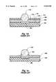
- FIG. 4illustrates a substrate assembly 400 of the present invention.
- the substrate assembly 400comprises a first substrate 402 with a plurality of conductive electrodes 404 disposed on a facing surface 406 of the first substrate 402.
- a palladium metal layer 408is disposed on each conductive electrode 404 by electroless plating.
- the substrate assembly 400further comprises a second substrate 410 with a plurality of conductive electrodes 412 disposed on a facing surface 414 of the second substrate 410.
- a palladium metal layer 416is also disposed on each conductive electrode 412.
- the first substrate 402 and the second substrate 410are mechanically attached to and in electrical communication with one another via a plurality of conductive polymer bumps 418 extending between the first substrate palladium metal layers 408 and the second substrate palladium metal layers 416.
- An under-fill encapsulant 420may be disposed between the first substrate 402 and the second substrate 410 for environmental protection and to enhance the attachment of the first substrate 402 and the second substrate 410.
- FIG. 5illustrates a first embodiment of a substrate/chip assembly 500 of the present invention.
- the substrate/chip assembly 500comprises a substrate 502 with a plurality of conductive electrodes 504 disposed on a facing surface 506 of the substrate 502.
- a palladium metal layer 508is disposed on each conductive electrode 504 by electroless plating.
- the substrate/chip assembly 500further comprises a semiconductor chip 510 with a plurality of bond pads 512 disposed on a facing surface 514 of the semiconductor chip 510.
- a palladium metal layer 516is also disposed on each bond pad 512.
- the substrate 502 and the semiconductor chip 510are mechanically attached to and in electrical communication with one another via a plurality of conductive polymer bumps 518 extending between the substrate palladium metal layers 508 and the semiconductor die palladium metal layers 516.
- An under-fill encapsulant 520may be disposed between the substrate 502 and the semiconductor die 510 for environmental protection and to enhance the attachment of the substrate 502 and the semiconductor chip 510.
- FIG. 6illustrates a second embodiment of a substrate/chip assembly 600 of the present invention.
- the substrate/chip assembly 600comprises a substrate 602 with a plurality of conductive electrodes 604 disposed on a facing surface 606 of the substrate 602.
- the conductive electrodes 604may comprise any suitable type metal electrode such as aluminum.
- the substrate/chip assembly 600further comprises a semiconductor chip 610 with a plurality of bond pads 612 disposed on a facing surface 614 of the semiconductor chip 610.
- a palladium metal layer 616is also disposed on each bond pad 612.
- the substrate 602 and the semiconductor chip 610are mechanically attached to and in electrical communication with one another via a plurality of conductive polymer bumps 618 extending between the substrate conductive electrodes 604 and the semiconductor die palladium metal layers 616.
- the conductive material in the conductive polymer bumps 618is capable of making electrical contact with the conductive electrodes 604 and penetrating any coating thereon whether an oxide coating or a passivation layer coating.
- An under-fill encapsulant 620may be disposed between the substrate 602 and the semiconductor die 610 for environmental protection and to enhance the attachment of the substrate 602 and the semiconductor chip 610.
- FIGS. 4, 5 and 6show substrates and/or semiconductor chips which use the palladium layered structures of the present invention, one of the substrates and/or semiconductor chips could be one of industry standard manufacture.
Landscapes
- Engineering & Computer Science (AREA)
- Microelectronics & Electronic Packaging (AREA)
- Computer Hardware Design (AREA)
- Power Engineering (AREA)
- Manufacturing & Machinery (AREA)
- Physics & Mathematics (AREA)
- Condensed Matter Physics & Semiconductors (AREA)
- General Physics & Mathematics (AREA)
- Ceramic Engineering (AREA)
- Wire Bonding (AREA)
Abstract
Description
Claims (26)
Priority Applications (8)
| Application Number | Priority Date | Filing Date | Title |
|---|---|---|---|
| US08/651,816US5925930A (en) | 1996-05-21 | 1996-05-21 | IC contacts with palladium layer and flexible conductive epoxy bumps |
| US09/227,072US6159769A (en) | 1996-05-21 | 1999-01-05 | Use of palladium in IC manufacturing |
| US09/645,947US6413862B1 (en) | 1996-05-21 | 2000-08-25 | Use of palladium in IC manufacturing |
| US10/116,962US6558979B2 (en) | 1996-05-21 | 2002-04-05 | Use of palladium in IC manufacturing with conductive polymer bump |
| US10/430,616US6939744B2 (en) | 1996-05-21 | 2003-05-05 | Use of palladium in IC manufacturing with conductive polymer bump |
| US11/008,654US20050104210A1 (en) | 1996-05-21 | 2004-12-09 | Use of palladium in IC manufacturing with conductive polymer bump |
| US11/145,632US7335988B2 (en) | 1996-05-21 | 2005-06-06 | Use of palladium in IC manufacturing with conductive polymer bump |
| US12/024,712US7759240B2 (en) | 1996-05-21 | 2008-02-01 | Use of palladium in IC manufacturing with conductive polymer bump |
Applications Claiming Priority (1)
| Application Number | Priority Date | Filing Date | Title |
|---|---|---|---|
| US08/651,816US5925930A (en) | 1996-05-21 | 1996-05-21 | IC contacts with palladium layer and flexible conductive epoxy bumps |
Related Child Applications (1)
| Application Number | Title | Priority Date | Filing Date |
|---|---|---|---|
| US09/227,072DivisionUS6159769A (en) | 1996-05-21 | 1999-01-05 | Use of palladium in IC manufacturing |
Publications (1)
| Publication Number | Publication Date |
|---|---|
| US5925930Atrue US5925930A (en) | 1999-07-20 |
Family
ID=24614340
Family Applications (3)
| Application Number | Title | Priority Date | Filing Date |
|---|---|---|---|
| US08/651,816Expired - LifetimeUS5925930A (en) | 1996-05-21 | 1996-05-21 | IC contacts with palladium layer and flexible conductive epoxy bumps |
| US09/227,072Expired - LifetimeUS6159769A (en) | 1996-05-21 | 1999-01-05 | Use of palladium in IC manufacturing |
| US09/645,947Expired - LifetimeUS6413862B1 (en) | 1996-05-21 | 2000-08-25 | Use of palladium in IC manufacturing |
Family Applications After (2)
| Application Number | Title | Priority Date | Filing Date |
|---|---|---|---|
| US09/227,072Expired - LifetimeUS6159769A (en) | 1996-05-21 | 1999-01-05 | Use of palladium in IC manufacturing |
| US09/645,947Expired - LifetimeUS6413862B1 (en) | 1996-05-21 | 2000-08-25 | Use of palladium in IC manufacturing |
Country Status (1)
| Country | Link |
|---|---|
| US (3) | US5925930A (en) |
Cited By (62)
| Publication number | Priority date | Publication date | Assignee | Title |
|---|---|---|---|---|
| US6002590A (en)* | 1998-03-24 | 1999-12-14 | Micron Technology, Inc. | Flexible trace surface circuit board and method for making flexible trace surface circuit board |
| US6118179A (en)* | 1999-08-27 | 2000-09-12 | Micron Technology, Inc. | Semiconductor component with external contact polymer support member and method of fabrication |
| US6143116A (en)* | 1996-09-26 | 2000-11-07 | Kyocera Corporation | Process for producing a multi-layer wiring board |
| US6189208B1 (en)* | 1998-09-11 | 2001-02-20 | Polymer Flip Chip Corp. | Flip chip mounting technique |
| US20010017414A1 (en)* | 1998-04-27 | 2001-08-30 | Gilleo Kenneth Burton | Flip chip with integrated mask and underfill |
| US6287890B1 (en) | 1999-10-18 | 2001-09-11 | Thin Film Module, Inc. | Low cost decal material used for packaging |
| US6300679B1 (en)* | 1998-06-01 | 2001-10-09 | Semiconductor Components Industries, Llc | Flexible substrate for packaging a semiconductor component |
| US6333104B1 (en)* | 2000-05-30 | 2001-12-25 | International Business Machines Corporation | Conductive polymer interconnection configurations |
| US20020000654A1 (en)* | 1997-12-26 | 2002-01-03 | Shuichi Matsuda | Semiconductor device |
| US6395633B1 (en)* | 2001-05-16 | 2002-05-28 | World Wiser Electrics Inc. | Method of forming micro-via |
| US6408511B1 (en)* | 2000-08-21 | 2002-06-25 | National Semiconductor, Inc. | Method of creating an enhanced BGA attachment in a low-temperature co-fired ceramic (LTCC) substrate |
| US6410415B1 (en) | 1999-03-23 | 2002-06-25 | Polymer Flip Chip Corporation | Flip chip mounting technique |
| US20020109233A1 (en)* | 2000-01-18 | 2002-08-15 | Micron Technology, Inc. | Process for providing seed layers for integrated circuit metallurgy |
| US6507118B1 (en)* | 2000-07-14 | 2003-01-14 | 3M Innovative Properties Company | Multi-metal layer circuit |
| US6555759B2 (en)* | 1999-09-17 | 2003-04-29 | George Tzanavaras | Interconnect structure |
| US6576495B1 (en) | 2000-08-30 | 2003-06-10 | Micron Technology, Inc. | Microelectronic assembly with pre-disposed fill material and associated method of manufacture |
| US6617675B2 (en)* | 2000-12-15 | 2003-09-09 | Matsushita Electric Industrial Co., Ltd. | Semiconductor device and semiconductor device assembly |
| US20030189243A1 (en)* | 2002-04-04 | 2003-10-09 | Tongbi Jiang | Microelectronic package with reduced underfill and methods for forming such packages |
| US20030203536A1 (en)* | 2001-12-12 | 2003-10-30 | Dias Rajen C. | Flip chip underfill process |
| US20030207490A1 (en)* | 2001-08-24 | 2003-11-06 | International Rectifier Corporation | Wafer level underfill and interconnect process |
| US6689635B1 (en)* | 1997-08-21 | 2004-02-10 | Micron Technology, Inc. | Apparatus and method for face-to-face connection of a die to a substrate with polymer electrodes |
| US20040087077A1 (en)* | 1999-08-27 | 2004-05-06 | Farnworth Warren M. | Electronic assembly having semiconductor component with polymer support member and method of fabrication |
| US20040099941A1 (en)* | 2002-11-27 | 2004-05-27 | International Rectifier Corporation | Flip-chip device having conductive connectors |
| US6743716B2 (en) | 2000-01-18 | 2004-06-01 | Micron Technology, Inc. | Structures and methods to enhance copper metallization |
| US6756298B2 (en) | 2000-01-18 | 2004-06-29 | Micron Technology, Inc. | Methods and apparatus for making integrated-circuit wiring from copper, silver, gold, and other metals |
| US6767818B1 (en)* | 2000-08-07 | 2004-07-27 | Industrial Technology Research Institute | Method for forming electrically conductive bumps and devices formed |
| US6779711B2 (en)* | 1999-05-14 | 2004-08-24 | International Business Machines Corporation | Self-aligned corrosion stop for copper C4 and wirebond |
| US20040201089A1 (en)* | 2003-03-20 | 2004-10-14 | Seiko Epson Corporation | Semiconductor devices and manufacturing methods therefore |
| US20040219783A1 (en)* | 2001-07-09 | 2004-11-04 | Micron Technology, Inc. | Copper dual damascene interconnect technology |
| US20050046040A1 (en)* | 2003-08-25 | 2005-03-03 | Advanced Semiconductor Engineering, Inc. | Flip chip stacked package |
| US20050045378A1 (en)* | 2003-08-29 | 2005-03-03 | Heng Mung Suan | Stacked microfeature devices and associated methods |
| US20050062153A1 (en)* | 2003-08-21 | 2005-03-24 | Seiko Epson Corporation | Mounting structure of electronic component, electro-optic device, electronic equipment, and method for mounting electronic component |
| US20050104228A1 (en)* | 2003-11-13 | 2005-05-19 | Rigg Sidney B. | Microelectronic devices, methods for forming vias in microelectronic devices, and methods for packaging microelectronic devices |
| US20050127504A1 (en)* | 2003-12-05 | 2005-06-16 | Hideo Imai | Semiconductor device, semiconductor chip, method for manufacturing semiconductor device, and electronic apparatus |
| US20050127478A1 (en)* | 2003-12-10 | 2005-06-16 | Hiatt William M. | Microelectronic devices and methods for filling vias in microelectronic devices |
| US6924553B2 (en)* | 2001-10-25 | 2005-08-02 | Seiko Epson Corporation | Semiconductor chip and wiring board with bumps formed on pads/land and on passivation/insulation film and manufacturing method of the same |
| US6939744B2 (en) | 1996-05-21 | 2005-09-06 | Micron Technology, Inc. | Use of palladium in IC manufacturing with conductive polymer bump |
| US20050277279A1 (en)* | 2004-06-14 | 2005-12-15 | Shijian Luo | Microfeature devices and methods for manufacturing microfeature devices |
| US6995470B2 (en) | 2000-05-31 | 2006-02-07 | Micron Technology, Inc. | Multilevel copper interconnects with low-k dielectrics and air gaps |
| US20060131746A1 (en)* | 2004-12-22 | 2006-06-22 | Sanyo Electric Co., Ltd. | Circuit device |
| US7067421B2 (en) | 2000-05-31 | 2006-06-27 | Micron Technology, Inc. | Multilevel copper interconnect with double passivation |
| US20060177970A1 (en)* | 2005-02-08 | 2006-08-10 | Micron Technology, Inc. | Methods of Adhering Microfeature Workpieces, Including A Chip, To A Support Member |
| US20070018337A1 (en)* | 2002-04-04 | 2007-01-25 | Micron Technology, Inc. | Method and apparatus for attaching microelectronic substrates and support members |
| US20070026575A1 (en)* | 2005-06-24 | 2007-02-01 | Subramanian Sankara J | No flow underfill device and method |
| US20070045812A1 (en)* | 2005-08-31 | 2007-03-01 | Micron Technology, Inc. | Microfeature assemblies including interconnect structures and methods for forming such interconnect structures |
| US7220665B2 (en) | 2003-08-05 | 2007-05-22 | Micron Technology, Inc. | H2 plasma treatment |
| US20070139977A1 (en)* | 2005-12-19 | 2007-06-21 | Endicott Interconnect Technologies, Inc. | Method of improving electrical connections in circuitized substrates |
| US20070155048A1 (en)* | 2005-12-29 | 2007-07-05 | Micron Technology, Inc. | Methods for packaging microelectronic devices and microelectronic devices formed using such methods |
| US7253521B2 (en) | 2000-01-18 | 2007-08-07 | Micron Technology, Inc. | Methods for making integrated-circuit wiring from copper, silver, gold, and other metals |
| US7262505B2 (en) | 2000-01-18 | 2007-08-28 | Micron Technology, Inc. | Selective electroless-plated copper metallization |
| US20070290337A1 (en)* | 2006-06-14 | 2007-12-20 | Ralf Otremba | Electrically Conductive Connection, Electronic Component and Method for Their Production |
| US20080048316A1 (en)* | 2006-08-25 | 2008-02-28 | Micron Technology, Inc. | Packaged microdevices and methods for manufacturing packaged microdevices |
| US20080050901A1 (en)* | 2006-08-23 | 2008-02-28 | Micron Technology, Inc. | Packaged microelectronic devices and methods for manufacturing packaged microelectronic devices |
| US20080054458A1 (en)* | 2006-08-10 | 2008-03-06 | Hiroshi Ozaki | Electronic device and method of manufacturing the same |
| US20090102323A1 (en)* | 2007-10-19 | 2009-04-23 | Seiko Epson Corporation | Electronic component, mounting structure thereof, and method for mounting electronic component |
| US20090166862A1 (en)* | 2007-12-27 | 2009-07-02 | Samsung Electro-Mechanics Co., Ltd. | Semiconductor device and method of manufacturing the same |
| US20090210055A1 (en)* | 2008-02-19 | 2009-08-20 | Industrial Technology Research Institute | Artificial optic nerve network module, artificial retina chip module, and method for fabricating the same |
| CN101217124B (en)* | 2008-01-18 | 2010-06-23 | 清华大学 | A low temperature flip chip welding method of macromolecule electric conducting material of template printing |
| CN101414809B (en)* | 2007-10-19 | 2011-04-06 | 精工爱普生株式会社 | Electronic component, mounting structure and mounting method thereof |
| US20150091177A1 (en)* | 2013-09-27 | 2015-04-02 | Samsung Electro-Mechanics Co., Ltd. | External connection terminal, semiconductor package having external connection terminal, and methods for manufacturing the same |
| US9704818B1 (en) | 2016-07-06 | 2017-07-11 | Nanya Technology Corporation | Semiconductor structure and manufacturing method thereof |
| WO2018208656A1 (en)* | 2017-05-08 | 2018-11-15 | Thin Film Electronics Asa | Electronic device having attach pads, an antenna and/or an inductor with printed palladium thereon, and methods of making the same |
Families Citing this family (10)
| Publication number | Priority date | Publication date | Assignee | Title |
|---|---|---|---|---|
| US6376352B1 (en)* | 1998-11-05 | 2002-04-23 | Texas Instruments Incorporated | Stud-cone bump for probe tips used in known good die carriers |
| US6544880B1 (en) | 1999-06-14 | 2003-04-08 | Micron Technology, Inc. | Method of improving copper interconnects of semiconductor devices for bonding |
| US7152291B2 (en) | 2002-04-15 | 2006-12-26 | Avx Corporation | Method for forming plated terminations |
| US6998334B2 (en)* | 2002-07-08 | 2006-02-14 | Micron Technology, Inc. | Semiconductor devices with permanent polymer stencil and method for manufacturing the same |
| US6852627B2 (en)* | 2003-03-05 | 2005-02-08 | Micron Technology, Inc. | Conductive through wafer vias |
| KR100577562B1 (en) | 2004-02-05 | 2006-05-08 | 삼성전자주식회사 | Fin transistor formation method and its structure |
| CN100468674C (en)* | 2004-11-25 | 2009-03-11 | 日本电气株式会社 | Semiconductor device and method of manufacturing the same, wiring board and method of manufacturing the same, semiconductor package, and electronic apparatus |
| TWI264787B (en)* | 2005-10-13 | 2006-10-21 | Phoenix Prec Technology Corp | Wafer structure with electroless plating metal connecting layer and method for fabricating the same |
| TWI339883B (en)* | 2007-02-02 | 2011-04-01 | Unimicron Technology Corp | Substrate structure for semiconductor package and manufacturing method thereof |
| CN102843856A (en)* | 2012-09-11 | 2012-12-26 | 厦门爱谱生电子科技有限公司 | Flexible circuit board welded with a plurality of conductive contact blocks and manufacture method thereof |
Citations (15)
| Publication number | Priority date | Publication date | Assignee | Title |
|---|---|---|---|---|
| US4182781A (en)* | 1977-09-21 | 1980-01-08 | Texas Instruments Incorporated | Low cost method for forming elevated metal bumps on integrated circuit bodies employing an aluminum/palladium metallization base for electroless plating |
| US4970571A (en)* | 1987-09-24 | 1990-11-13 | Kabushiki Kaisha Toshiba | Bump and method of manufacturing the same |
| US5196371A (en)* | 1989-12-18 | 1993-03-23 | Epoxy Technology, Inc. | Flip chip bonding method using electrically conductive polymer bumps |
| US5258577A (en)* | 1991-11-22 | 1993-11-02 | Clements James R | Die mounting with uniaxial conductive adhesive |
| US5468681A (en)* | 1989-08-28 | 1995-11-21 | Lsi Logic Corporation | Process for interconnecting conductive substrates using an interposer having conductive plastic filled vias |
| US5468995A (en)* | 1994-07-05 | 1995-11-21 | Motorola, Inc. | Semiconductor device having compliant columnar electrical connections |
| US5478007A (en)* | 1993-04-14 | 1995-12-26 | Amkor Electronics, Inc. | Method for interconnection of integrated circuit chip and substrate |
| US5485038A (en)* | 1993-07-15 | 1996-01-16 | Hughes Aircraft Company | Microelectronic circuit substrate structure including photoimageable epoxy dielectric layers |
| US5486721A (en)* | 1993-04-10 | 1996-01-23 | W.C. Heraeus Gmbh | Lead frame for integrated circuits |
| US5489804A (en)* | 1989-08-28 | 1996-02-06 | Lsi Logic Corporation | Flexible preformed planar structures for interposing between a chip and a substrate |
| US5491612A (en)* | 1995-02-21 | 1996-02-13 | Fairchild Space And Defense Corporation | Three-dimensional modular assembly of integrated circuits |
| US5493437A (en)* | 1993-09-13 | 1996-02-20 | Motorola | External communication link for a credit card pager |
| US5521432A (en)* | 1991-10-14 | 1996-05-28 | Fujitsu Limited | Semiconductor device having improved leads comprising palladium plated nickel |
| US5561320A (en)* | 1992-06-04 | 1996-10-01 | Texas Instruments Incorporated | Silver spot/palladium plate lead frame finish |
| US5674780A (en)* | 1995-07-24 | 1997-10-07 | Motorola, Inc. | Method of forming an electrically conductive polymer bump over an aluminum electrode |
- 1996
- 1996-05-21USUS08/651,816patent/US5925930A/ennot_activeExpired - Lifetime
- 1999
- 1999-01-05USUS09/227,072patent/US6159769A/ennot_activeExpired - Lifetime
- 2000
- 2000-08-25USUS09/645,947patent/US6413862B1/ennot_activeExpired - Lifetime
Patent Citations (15)
| Publication number | Priority date | Publication date | Assignee | Title |
|---|---|---|---|---|
| US4182781A (en)* | 1977-09-21 | 1980-01-08 | Texas Instruments Incorporated | Low cost method for forming elevated metal bumps on integrated circuit bodies employing an aluminum/palladium metallization base for electroless plating |
| US4970571A (en)* | 1987-09-24 | 1990-11-13 | Kabushiki Kaisha Toshiba | Bump and method of manufacturing the same |
| US5489804A (en)* | 1989-08-28 | 1996-02-06 | Lsi Logic Corporation | Flexible preformed planar structures for interposing between a chip and a substrate |
| US5468681A (en)* | 1989-08-28 | 1995-11-21 | Lsi Logic Corporation | Process for interconnecting conductive substrates using an interposer having conductive plastic filled vias |
| US5196371A (en)* | 1989-12-18 | 1993-03-23 | Epoxy Technology, Inc. | Flip chip bonding method using electrically conductive polymer bumps |
| US5521432A (en)* | 1991-10-14 | 1996-05-28 | Fujitsu Limited | Semiconductor device having improved leads comprising palladium plated nickel |
| US5258577A (en)* | 1991-11-22 | 1993-11-02 | Clements James R | Die mounting with uniaxial conductive adhesive |
| US5561320A (en)* | 1992-06-04 | 1996-10-01 | Texas Instruments Incorporated | Silver spot/palladium plate lead frame finish |
| US5486721A (en)* | 1993-04-10 | 1996-01-23 | W.C. Heraeus Gmbh | Lead frame for integrated circuits |
| US5478007A (en)* | 1993-04-14 | 1995-12-26 | Amkor Electronics, Inc. | Method for interconnection of integrated circuit chip and substrate |
| US5485038A (en)* | 1993-07-15 | 1996-01-16 | Hughes Aircraft Company | Microelectronic circuit substrate structure including photoimageable epoxy dielectric layers |
| US5493437A (en)* | 1993-09-13 | 1996-02-20 | Motorola | External communication link for a credit card pager |
| US5468995A (en)* | 1994-07-05 | 1995-11-21 | Motorola, Inc. | Semiconductor device having compliant columnar electrical connections |
| US5491612A (en)* | 1995-02-21 | 1996-02-13 | Fairchild Space And Defense Corporation | Three-dimensional modular assembly of integrated circuits |
| US5674780A (en)* | 1995-07-24 | 1997-10-07 | Motorola, Inc. | Method of forming an electrically conductive polymer bump over an aluminum electrode |
Cited By (145)
| Publication number | Priority date | Publication date | Assignee | Title |
|---|---|---|---|---|
| US7759240B2 (en) | 1996-05-21 | 2010-07-20 | Micron Technology, Inc. | Use of palladium in IC manufacturing with conductive polymer bump |
| US20050218510A1 (en)* | 1996-05-21 | 2005-10-06 | Farnworth Warren M | Use of palladium in IC manufacturing with conductive polymer bump |
| US20080119038A1 (en)* | 1996-05-21 | 2008-05-22 | Micron Technology, Inc. | Use of palladium in ic manufacturing with conductive polymer bump |
| US6939744B2 (en) | 1996-05-21 | 2005-09-06 | Micron Technology, Inc. | Use of palladium in IC manufacturing with conductive polymer bump |
| US7335988B2 (en) | 1996-05-21 | 2008-02-26 | Micron Technology, Inc. | Use of palladium in IC manufacturing with conductive polymer bump |
| US6143116A (en)* | 1996-09-26 | 2000-11-07 | Kyocera Corporation | Process for producing a multi-layer wiring board |
| US6689635B1 (en)* | 1997-08-21 | 2004-02-10 | Micron Technology, Inc. | Apparatus and method for face-to-face connection of a die to a substrate with polymer electrodes |
| US6794750B2 (en)* | 1997-12-26 | 2004-09-21 | Nec Electronics Corporation | Semiconductor device |
| US20020000654A1 (en)* | 1997-12-26 | 2002-01-03 | Shuichi Matsuda | Semiconductor device |
| US6002590A (en)* | 1998-03-24 | 1999-12-14 | Micron Technology, Inc. | Flexible trace surface circuit board and method for making flexible trace surface circuit board |
| US20010017414A1 (en)* | 1998-04-27 | 2001-08-30 | Gilleo Kenneth Burton | Flip chip with integrated mask and underfill |
| US6300679B1 (en)* | 1998-06-01 | 2001-10-09 | Semiconductor Components Industries, Llc | Flexible substrate for packaging a semiconductor component |
| US6189208B1 (en)* | 1998-09-11 | 2001-02-20 | Polymer Flip Chip Corp. | Flip chip mounting technique |
| US6410415B1 (en) | 1999-03-23 | 2002-06-25 | Polymer Flip Chip Corporation | Flip chip mounting technique |
| US6779711B2 (en)* | 1999-05-14 | 2004-08-24 | International Business Machines Corporation | Self-aligned corrosion stop for copper C4 and wirebond |
| US6118179A (en)* | 1999-08-27 | 2000-09-12 | Micron Technology, Inc. | Semiconductor component with external contact polymer support member and method of fabrication |
| US6909194B2 (en) | 1999-08-27 | 2005-06-21 | Micron Technology, Inc. | Electronic assembly having semiconductor component with polymer support member and method of fabrication |
| US20040087077A1 (en)* | 1999-08-27 | 2004-05-06 | Farnworth Warren M. | Electronic assembly having semiconductor component with polymer support member and method of fabrication |
| US6756253B1 (en) | 1999-08-27 | 2004-06-29 | Micron Technology, Inc. | Method for fabricating a semiconductor component with external contact polymer support layer |
| US6180504B1 (en)* | 1999-08-27 | 2001-01-30 | Micron Technology, Inc. | Method for fabricating a semiconductor component with external polymer support layer |
| US6555759B2 (en)* | 1999-09-17 | 2003-04-29 | George Tzanavaras | Interconnect structure |
| US6586846B2 (en) | 1999-10-18 | 2003-07-01 | Thin Film Module, Inc. | Low cost decal material used for packaging |
| US6287890B1 (en) | 1999-10-18 | 2001-09-11 | Thin Film Module, Inc. | Low cost decal material used for packaging |
| US6743716B2 (en) | 2000-01-18 | 2004-06-01 | Micron Technology, Inc. | Structures and methods to enhance copper metallization |
| US7535103B2 (en) | 2000-01-18 | 2009-05-19 | Micron Technology, Inc. | Structures and methods to enhance copper metallization |
| US7105914B2 (en) | 2000-01-18 | 2006-09-12 | Micron Technology, Inc. | Integrated circuit and seed layers |
| US7394157B2 (en) | 2000-01-18 | 2008-07-01 | Micron Technology, Inc. | Integrated circuit and seed layers |
| US8779596B2 (en) | 2000-01-18 | 2014-07-15 | Micron Technology, Inc. | Structures and methods to enhance copper metallization |
| US7402516B2 (en) | 2000-01-18 | 2008-07-22 | Micron Technology, Inc. | Method for making integrated circuits |
| US6756298B2 (en) | 2000-01-18 | 2004-06-29 | Micron Technology, Inc. | Methods and apparatus for making integrated-circuit wiring from copper, silver, gold, and other metals |
| US7253521B2 (en) | 2000-01-18 | 2007-08-07 | Micron Technology, Inc. | Methods for making integrated-circuit wiring from copper, silver, gold, and other metals |
| US7670469B2 (en) | 2000-01-18 | 2010-03-02 | Micron Technology, Inc. | Methods and apparatus for making integrated-circuit wiring from copper, silver, gold, and other metals |
| US20020109233A1 (en)* | 2000-01-18 | 2002-08-15 | Micron Technology, Inc. | Process for providing seed layers for integrated circuit metallurgy |
| US7378737B2 (en) | 2000-01-18 | 2008-05-27 | Micron Technology, Inc. | Structures and methods to enhance copper metallization |
| US7262505B2 (en) | 2000-01-18 | 2007-08-28 | Micron Technology, Inc. | Selective electroless-plated copper metallization |
| US7262130B1 (en) | 2000-01-18 | 2007-08-28 | Micron Technology, Inc. | Methods for making integrated-circuit wiring from copper, silver, gold, and other metals |
| US7368378B2 (en) | 2000-01-18 | 2008-05-06 | Micron Technology, Inc. | Methods for making integrated-circuit wiring from copper, silver, gold, and other metals |
| US7745934B2 (en) | 2000-01-18 | 2010-06-29 | Micron Technology, Inc. | Integrated circuit and seed layers |
| US7285196B2 (en) | 2000-01-18 | 2007-10-23 | Micron Technology, Inc. | Methods and apparatus for making integrated-circuit wiring from copper, silver, gold, and other metals |
| US7301190B2 (en) | 2000-01-18 | 2007-11-27 | Micron Technology, Inc. | Structures and methods to enhance copper metallization |
| US20020028327A1 (en)* | 2000-05-30 | 2002-03-07 | Perry Charles H. | Conductive polymer interconnection configurations |
| US6858111B2 (en) | 2000-05-30 | 2005-02-22 | International Business Machines Corporation | Conductive polymer interconnection configurations |
| US6333104B1 (en)* | 2000-05-30 | 2001-12-25 | International Business Machines Corporation | Conductive polymer interconnection configurations |
| US7091611B2 (en) | 2000-05-31 | 2006-08-15 | Micron Technology, Inc. | Multilevel copper interconnects with low-k dielectrics and air gaps |
| US7067421B2 (en) | 2000-05-31 | 2006-06-27 | Micron Technology, Inc. | Multilevel copper interconnect with double passivation |
| US6995470B2 (en) | 2000-05-31 | 2006-02-07 | Micron Technology, Inc. | Multilevel copper interconnects with low-k dielectrics and air gaps |
| US6507118B1 (en)* | 2000-07-14 | 2003-01-14 | 3M Innovative Properties Company | Multi-metal layer circuit |
| US6767818B1 (en)* | 2000-08-07 | 2004-07-27 | Industrial Technology Research Institute | Method for forming electrically conductive bumps and devices formed |
| US6408511B1 (en)* | 2000-08-21 | 2002-06-25 | National Semiconductor, Inc. | Method of creating an enhanced BGA attachment in a low-temperature co-fired ceramic (LTCC) substrate |
| US6576495B1 (en) | 2000-08-30 | 2003-06-10 | Micron Technology, Inc. | Microelectronic assembly with pre-disposed fill material and associated method of manufacture |
| US6661104B2 (en)* | 2000-08-30 | 2003-12-09 | Micron Technology, Inc. | Microelectronic assembly with pre-disposed fill material and associated method of manufacture |
| US6617675B2 (en)* | 2000-12-15 | 2003-09-09 | Matsushita Electric Industrial Co., Ltd. | Semiconductor device and semiconductor device assembly |
| US6395633B1 (en)* | 2001-05-16 | 2002-05-28 | World Wiser Electrics Inc. | Method of forming micro-via |
| US20040219783A1 (en)* | 2001-07-09 | 2004-11-04 | Micron Technology, Inc. | Copper dual damascene interconnect technology |
| US6967412B2 (en)* | 2001-08-24 | 2005-11-22 | International Rectifier Corporation | Wafer level underfill and interconnect process |
| US20030207490A1 (en)* | 2001-08-24 | 2003-11-06 | International Rectifier Corporation | Wafer level underfill and interconnect process |
| US6924553B2 (en)* | 2001-10-25 | 2005-08-02 | Seiko Epson Corporation | Semiconductor chip and wiring board with bumps formed on pads/land and on passivation/insulation film and manufacturing method of the same |
| US6815831B2 (en)* | 2001-12-12 | 2004-11-09 | Intel Corporation | Flip-chip device with multi-layered underfill having graded coefficient of thermal expansion |
| US20030203536A1 (en)* | 2001-12-12 | 2003-10-30 | Dias Rajen C. | Flip chip underfill process |
| US6844618B2 (en) | 2002-04-04 | 2005-01-18 | Micron Technology, Inc. | Microelectronic package with reduced underfill and methods for forming such packages |
| US20050016751A1 (en)* | 2002-04-04 | 2005-01-27 | Tongbi Jiang | Microelectronic package with reduced underfill and methods for forming such packages |
| US7615871B2 (en) | 2002-04-04 | 2009-11-10 | Micron Technology, Inc. | Method and apparatus for attaching microelectronic substrates and support members |
| US20070018337A1 (en)* | 2002-04-04 | 2007-01-25 | Micron Technology, Inc. | Method and apparatus for attaching microelectronic substrates and support members |
| US20070020811A1 (en)* | 2002-04-04 | 2007-01-25 | Micron Technology, Inc. | Method and apparatus for attaching microelectronic substrates and support members |
| US20030189243A1 (en)* | 2002-04-04 | 2003-10-09 | Tongbi Jiang | Microelectronic package with reduced underfill and methods for forming such packages |
| US6900080B2 (en) | 2002-04-04 | 2005-05-31 | Micron Technology, Inc. | Microelectronic package with reduced underfill and methods for forming such packages |
| US7088004B2 (en) | 2002-11-27 | 2006-08-08 | International Rectifier Corporation | Flip-chip device having conductive connectors |
| US20040099941A1 (en)* | 2002-11-27 | 2004-05-27 | International Rectifier Corporation | Flip-chip device having conductive connectors |
| US20040201089A1 (en)* | 2003-03-20 | 2004-10-14 | Seiko Epson Corporation | Semiconductor devices and manufacturing methods therefore |
| US7220665B2 (en) | 2003-08-05 | 2007-05-22 | Micron Technology, Inc. | H2 plasma treatment |
| US7504674B2 (en) | 2003-08-05 | 2009-03-17 | Micron Technology, Inc. | Electronic apparatus having a core conductive structure within an insulating layer |
| US20050062153A1 (en)* | 2003-08-21 | 2005-03-24 | Seiko Epson Corporation | Mounting structure of electronic component, electro-optic device, electronic equipment, and method for mounting electronic component |
| US7122896B2 (en)* | 2003-08-21 | 2006-10-17 | Seiko Epson Corporation | Mounting structure of electronic component, electro-optic device, electronic equipment, and method for mounting electronic component |
| US7291924B2 (en)* | 2003-08-25 | 2007-11-06 | Advanced Semiconductor Engineering, Inc. | Flip chip stacked package |
| US20050046040A1 (en)* | 2003-08-25 | 2005-03-03 | Advanced Semiconductor Engineering, Inc. | Flip chip stacked package |
| US9515046B2 (en) | 2003-08-29 | 2016-12-06 | Micron Technology, Inc. | Stacked microfeature devices and associated methods |
| US10062667B2 (en) | 2003-08-29 | 2018-08-28 | Micron Technology, Inc. | Stacked microfeature devices and associated methods |
| US11887970B2 (en) | 2003-08-29 | 2024-01-30 | Micron Technology, Inc. | Stacked microfeature devices and associated methods |
| US8400780B2 (en) | 2003-08-29 | 2013-03-19 | Micron Technology, Inc. | Stacked microfeature devices |
| US20100258939A1 (en)* | 2003-08-29 | 2010-10-14 | Micron Technology, Inc. | Stacked microfeature devices and associated methods |
| US20050045378A1 (en)* | 2003-08-29 | 2005-03-03 | Heng Mung Suan | Stacked microfeature devices and associated methods |
| US11373979B2 (en) | 2003-08-29 | 2022-06-28 | Micron Technology, Inc. | Stacked microfeature devices and associated methods |
| US7071421B2 (en) | 2003-08-29 | 2006-07-04 | Micron Technology, Inc. | Stacked microfeature devices and associated methods |
| US7742313B2 (en) | 2003-08-29 | 2010-06-22 | Micron Technology, Inc. | Stacked microfeature devices |
| US7759800B2 (en) | 2003-11-13 | 2010-07-20 | Micron Technology, Inc. | Microelectronics devices, having vias, and packaged microelectronic devices having vias |
| US20050104228A1 (en)* | 2003-11-13 | 2005-05-19 | Rigg Sidney B. | Microelectronic devices, methods for forming vias in microelectronic devices, and methods for packaging microelectronic devices |
| US7091124B2 (en) | 2003-11-13 | 2006-08-15 | Micron Technology, Inc. | Methods for forming vias in microelectronic devices, and methods for packaging microelectronic devices |
| US9653420B2 (en) | 2003-11-13 | 2017-05-16 | Micron Technology, Inc. | Microelectronic devices and methods for filling vias in microelectronic devices |
| US7413979B2 (en) | 2003-11-13 | 2008-08-19 | Micron Technology, Inc. | Methods for forming vias in microelectronic devices, and methods for packaging microelectronic devices |
| US20050127504A1 (en)* | 2003-12-05 | 2005-06-16 | Hideo Imai | Semiconductor device, semiconductor chip, method for manufacturing semiconductor device, and electronic apparatus |
| US7528487B2 (en)* | 2003-12-05 | 2009-05-05 | Seiko Epson Corporation | Semiconductor device having insulating material dispersed with conductive particles which establish electrical connection by penetrating to both copper conductive layer and land of wiring board |
| US8748311B2 (en) | 2003-12-10 | 2014-06-10 | Micron Technology, Inc. | Microelectronic devices and methods for filing vias in microelectronic devices |
| US11177175B2 (en) | 2003-12-10 | 2021-11-16 | Micron Technology, Inc. | Microelectronic devices and methods for filling vias in microelectronic devices |
| US20050127478A1 (en)* | 2003-12-10 | 2005-06-16 | Hiatt William M. | Microelectronic devices and methods for filling vias in microelectronic devices |
| US8084866B2 (en) | 2003-12-10 | 2011-12-27 | Micron Technology, Inc. | Microelectronic devices and methods for filling vias in microelectronic devices |
| US7253089B2 (en) | 2004-06-14 | 2007-08-07 | Micron Technology, Inc. | Microfeature devices and methods for manufacturing microfeature devices |
| US7199037B2 (en) | 2004-06-14 | 2007-04-03 | Micron Technology, Inc. | Microfeature devices and methods for manufacturing microfeature devices |
| US20050277279A1 (en)* | 2004-06-14 | 2005-12-15 | Shijian Luo | Microfeature devices and methods for manufacturing microfeature devices |
| US7411297B2 (en) | 2004-06-14 | 2008-08-12 | Micron Technology, Inc. | Microfeature devices and methods for manufacturing microfeature devices |
| US20060189118A1 (en)* | 2004-06-14 | 2006-08-24 | Micron Technology, Inc. | Microfeature devices and methods for manufacturing microfeature devices |
| US20060131746A1 (en)* | 2004-12-22 | 2006-06-22 | Sanyo Electric Co., Ltd. | Circuit device |
| US8093699B2 (en)* | 2004-12-22 | 2012-01-10 | Sanyo Electric Co., Ltd. | Circuit device with circuit board and semiconductor chip mounted thereon |
| US8278751B2 (en) | 2005-02-08 | 2012-10-02 | Micron Technology, Inc. | Methods of adhering microfeature workpieces, including a chip, to a support member |
| US7518237B2 (en) | 2005-02-08 | 2009-04-14 | Micron Technology, Inc. | Microfeature systems including adhered microfeature workpieces and support members |
| US20060177970A1 (en)* | 2005-02-08 | 2006-08-10 | Micron Technology, Inc. | Methods of Adhering Microfeature Workpieces, Including A Chip, To A Support Member |
| US20060189036A1 (en)* | 2005-02-08 | 2006-08-24 | Micron Technology, Inc. | Methods and systems for adhering microfeature workpieces to support members |
| US9064973B2 (en) | 2005-02-08 | 2015-06-23 | Micron Technology, Inc. | Die attached to a support member by a plurality of adhesive members |
| US20070026575A1 (en)* | 2005-06-24 | 2007-02-01 | Subramanian Sankara J | No flow underfill device and method |
| US20070045812A1 (en)* | 2005-08-31 | 2007-03-01 | Micron Technology, Inc. | Microfeature assemblies including interconnect structures and methods for forming such interconnect structures |
| US20070139977A1 (en)* | 2005-12-19 | 2007-06-21 | Endicott Interconnect Technologies, Inc. | Method of improving electrical connections in circuitized substrates |
| US7629559B2 (en)* | 2005-12-19 | 2009-12-08 | Endicott Interconnect Technologies, Inc. | Method of improving electrical connections in circuitized substrates |
| US8203213B2 (en) | 2005-12-29 | 2012-06-19 | Micron Technology, Inc. | Methods for packaging microelectronic devices and microelectronic devices formed using such methods |
| US20100276814A1 (en)* | 2005-12-29 | 2010-11-04 | Micron Technology, Inc. | Methods for packaging microelectronic devices and microelectronic devices formed using such methods |
| US7759221B2 (en) | 2005-12-29 | 2010-07-20 | Micron Technology, Inc. | Methods for packaging microelectronic devices and microelectronic devices formed using such methods |
| US8772947B2 (en) | 2005-12-29 | 2014-07-08 | Micron Technology, Inc. | Methods for packaging microelectronic devices and microelectronic devices formed using such methods |
| US20070155048A1 (en)* | 2005-12-29 | 2007-07-05 | Micron Technology, Inc. | Methods for packaging microelectronic devices and microelectronic devices formed using such methods |
| US20070290337A1 (en)* | 2006-06-14 | 2007-12-20 | Ralf Otremba | Electrically Conductive Connection, Electronic Component and Method for Their Production |
| US20080054458A1 (en)* | 2006-08-10 | 2008-03-06 | Hiroshi Ozaki | Electronic device and method of manufacturing the same |
| US7749882B2 (en) | 2006-08-23 | 2010-07-06 | Micron Technology, Inc. | Packaged microelectronic devices and methods for manufacturing packaged microelectronic devices |
| US10083931B2 (en) | 2006-08-23 | 2018-09-25 | Micron Technology, Inc. | Packaged microelectronic devices having stacked interconnect elements and methods for manufacturing the same |
| US9240385B2 (en) | 2006-08-23 | 2016-01-19 | Micron Technology, Inc. | Packaged microelectronic devices and methods for manufacturing packaged microelectronic devices |
| US20100237494A1 (en)* | 2006-08-23 | 2010-09-23 | Micron Technology, Inc. | Packaged microelectronic devices and methods for manufacturing packaged microelectronic devices |
| US20080050901A1 (en)* | 2006-08-23 | 2008-02-28 | Micron Technology, Inc. | Packaged microelectronic devices and methods for manufacturing packaged microelectronic devices |
| US11217556B2 (en) | 2006-08-23 | 2022-01-04 | Micron Technology, Inc. | Packaged microelectronic devices having stacked interconnect elements and methods for manufacturing the same |
| US8922002B2 (en) | 2006-08-23 | 2014-12-30 | Micron Technology, Inc. | Packaged microelectronic devices and methods for manufacturing packaged microelectronic devices |
| US8987885B2 (en) | 2006-08-25 | 2015-03-24 | Micron Technology, Inc. | Packaged microdevices and methods for manufacturing packaged microdevices |
| US8354301B2 (en) | 2006-08-25 | 2013-01-15 | Micron Technology, Inc. | Packaged microdevices and methods for manufacturing packaged microdevices |
| US20080048316A1 (en)* | 2006-08-25 | 2008-02-28 | Micron Technology, Inc. | Packaged microdevices and methods for manufacturing packaged microdevices |
| US20110104857A1 (en)* | 2006-08-25 | 2011-05-05 | Micron Technology, Inc. | Packaged microdevices and methods for manufacturing packaged microdevices |
| US7868440B2 (en) | 2006-08-25 | 2011-01-11 | Micron Technology, Inc. | Packaged microdevices and methods for manufacturing packaged microdevices |
| CN102170274B (en)* | 2007-10-19 | 2014-11-12 | 精工爱普生株式会社 | Electronic component and mounting structure and mounting method thereof |
| US20090102323A1 (en)* | 2007-10-19 | 2009-04-23 | Seiko Epson Corporation | Electronic component, mounting structure thereof, and method for mounting electronic component |
| US20100237749A1 (en)* | 2007-10-19 | 2010-09-23 | Seiko Epson Corporation | Electronic component, mounting structure thereof, and method for mounting electronic component |
| US8274201B2 (en) | 2007-10-19 | 2012-09-25 | Seiko Epson Corporation | Electronic component, mounting structure thereof, and method for mounting electronic component |
| US7755261B2 (en)* | 2007-10-19 | 2010-07-13 | Seiko Epson Corporation | Electronic component, mounting structure thereof, and method for mounting electronic component |
| US8102099B2 (en) | 2007-10-19 | 2012-01-24 | Seiko Epson Corporation | Electronic component, mounting structure thereof, and method for mounting electronic component |
| CN102170274A (en)* | 2007-10-19 | 2011-08-31 | 精工爱普生株式会社 | Electronic component and mounting structure and mounting method thereof |
| CN101414809B (en)* | 2007-10-19 | 2011-04-06 | 精工爱普生株式会社 | Electronic component, mounting structure and mounting method thereof |
| US20090166862A1 (en)* | 2007-12-27 | 2009-07-02 | Samsung Electro-Mechanics Co., Ltd. | Semiconductor device and method of manufacturing the same |
| CN101217124B (en)* | 2008-01-18 | 2010-06-23 | 清华大学 | A low temperature flip chip welding method of macromolecule electric conducting material of template printing |
| US20090210055A1 (en)* | 2008-02-19 | 2009-08-20 | Industrial Technology Research Institute | Artificial optic nerve network module, artificial retina chip module, and method for fabricating the same |
| US9105616B2 (en)* | 2013-09-27 | 2015-08-11 | Samsung Electro-Mechanics Co., Ltd. | External connection terminal, semiconductor package having external connection terminal, and methods for manufacturing the same |
| US20150091177A1 (en)* | 2013-09-27 | 2015-04-02 | Samsung Electro-Mechanics Co., Ltd. | External connection terminal, semiconductor package having external connection terminal, and methods for manufacturing the same |
| US9704818B1 (en) | 2016-07-06 | 2017-07-11 | Nanya Technology Corporation | Semiconductor structure and manufacturing method thereof |
| WO2018208656A1 (en)* | 2017-05-08 | 2018-11-15 | Thin Film Electronics Asa | Electronic device having attach pads, an antenna and/or an inductor with printed palladium thereon, and methods of making the same |
Also Published As
| Publication number | Publication date |
|---|---|
| US6159769A (en) | 2000-12-12 |
| US6413862B1 (en) | 2002-07-02 |
Similar Documents
| Publication | Publication Date | Title |
|---|---|---|
| US5925930A (en) | IC contacts with palladium layer and flexible conductive epoxy bumps | |
| US7759240B2 (en) | Use of palladium in IC manufacturing with conductive polymer bump | |
| US6221753B1 (en) | Flip chip technique for chip assembly | |
| US6204095B1 (en) | Method of forming overmolded chip scale package and resulting product | |
| US7314817B2 (en) | Microelectronic device interconnects | |
| US5783465A (en) | Compliant bump technology | |
| US6906417B2 (en) | Ball grid array utilizing solder balls having a core material covered by a metal layer | |
| US6245594B1 (en) | Methods for forming conductive micro-bumps and recessed contacts for flip-chip technology and method of flip-chip assembly | |
| US5844320A (en) | Semiconductor unit with semiconductor device mounted with conductive adhesive | |
| US6844052B2 (en) | Method for underfilling semiconductor components | |
| US5897336A (en) | Direct chip attach for low alpha emission interconnect system | |
| US6707149B2 (en) | Low cost and compliant microelectronic packages for high i/o and fine pitch | |
| JPH08255965A (en) | Microchip module assembly | |
| US6335271B1 (en) | Method of forming semiconductor device bump electrodes | |
| US20020086515A1 (en) | Method of manufacturing bump electrodes and a method of manufacturing a semiconductor device | |
| US20010013655A1 (en) | Methods of making microelectronic connections with liquid conductive elements | |
| US6960518B1 (en) | Buildup substrate pad pre-solder bump manufacturing | |
| US20070085220A1 (en) | Re-enforced ball-grid array packages for semiconductor products | |
| US6831361B2 (en) | Flip chip technique for chip assembly | |
| KR100310037B1 (en) | Method for fabricating flexible printed circuit boad with a plurality of chip | |
| JPH1187561A (en) | Semiconductor device, semiconductor chip mounting member, semiconductor chip and production thereof | |
| JPH0973934A (en) | connector |
Legal Events
| Date | Code | Title | Description |
|---|---|---|---|
| AS | Assignment | Owner name:MICRO TECHNOLOGY, INC., IDAHO Free format text:ASSIGNMENT OF ASSIGNORS INTEREST;ASSIGNORS:FARNWORTH, WARREN M.;AKRAM, SALMAN;REEL/FRAME:008017/0585 Effective date:19960514 | |
| FEPP | Fee payment procedure | Free format text:PAYOR NUMBER ASSIGNED (ORIGINAL EVENT CODE: ASPN); ENTITY STATUS OF PATENT OWNER: LARGE ENTITY | |
| STCF | Information on status: patent grant | Free format text:PATENTED CASE | |
| CC | Certificate of correction | ||
| FPAY | Fee payment | Year of fee payment:4 | |
| FPAY | Fee payment | Year of fee payment:8 | |
| FPAY | Fee payment | Year of fee payment:12 | |
| AS | Assignment | Owner name:U.S. BANK NATIONAL ASSOCIATION, AS COLLATERAL AGENT, CALIFORNIA Free format text:SECURITY INTEREST;ASSIGNOR:MICRON TECHNOLOGY, INC.;REEL/FRAME:038669/0001 Effective date:20160426 Owner name:U.S. BANK NATIONAL ASSOCIATION, AS COLLATERAL AGEN Free format text:SECURITY INTEREST;ASSIGNOR:MICRON TECHNOLOGY, INC.;REEL/FRAME:038669/0001 Effective date:20160426 | |
| AS | Assignment | Owner name:MORGAN STANLEY SENIOR FUNDING, INC., AS COLLATERAL AGENT, MARYLAND Free format text:PATENT SECURITY AGREEMENT;ASSIGNOR:MICRON TECHNOLOGY, INC.;REEL/FRAME:038954/0001 Effective date:20160426 Owner name:MORGAN STANLEY SENIOR FUNDING, INC., AS COLLATERAL Free format text:PATENT SECURITY AGREEMENT;ASSIGNOR:MICRON TECHNOLOGY, INC.;REEL/FRAME:038954/0001 Effective date:20160426 | |
| AS | Assignment | Owner name:U.S. BANK NATIONAL ASSOCIATION, AS COLLATERAL AGENT, CALIFORNIA Free format text:CORRECTIVE ASSIGNMENT TO CORRECT THE REPLACE ERRONEOUSLY FILED PATENT #7358718 WITH THE CORRECT PATENT #7358178 PREVIOUSLY RECORDED ON REEL 038669 FRAME 0001. ASSIGNOR(S) HEREBY CONFIRMS THE SECURITY INTEREST;ASSIGNOR:MICRON TECHNOLOGY, INC.;REEL/FRAME:043079/0001 Effective date:20160426 Owner name:U.S. BANK NATIONAL ASSOCIATION, AS COLLATERAL AGEN Free format text:CORRECTIVE ASSIGNMENT TO CORRECT THE REPLACE ERRONEOUSLY FILED PATENT #7358718 WITH THE CORRECT PATENT #7358178 PREVIOUSLY RECORDED ON REEL 038669 FRAME 0001. ASSIGNOR(S) HEREBY CONFIRMS THE SECURITY INTEREST;ASSIGNOR:MICRON TECHNOLOGY, INC.;REEL/FRAME:043079/0001 Effective date:20160426 | |
| AS | Assignment | Owner name:MICRON TECHNOLOGY, INC., IDAHO Free format text:RELEASE BY SECURED PARTY;ASSIGNOR:U.S. BANK NATIONAL ASSOCIATION, AS COLLATERAL AGENT;REEL/FRAME:047243/0001 Effective date:20180629 | |
| AS | Assignment | Owner name:MICRON TECHNOLOGY, INC., IDAHO Free format text:RELEASE BY SECURED PARTY;ASSIGNOR:MORGAN STANLEY SENIOR FUNDING, INC., AS COLLATERAL AGENT;REEL/FRAME:050937/0001 Effective date:20190731 |