US5925577A - Method for forming via contact hole in a semiconductor device - Google Patents
Method for forming via contact hole in a semiconductor deviceDownload PDFInfo
- Publication number
- US5925577A US5925577AUS08/943,891US94389197AUS5925577AUS 5925577 AUS5925577 AUS 5925577AUS 94389197 AUS94389197 AUS 94389197AUS 5925577 AUS5925577 AUS 5925577A
- Authority
- US
- United States
- Prior art keywords
- metal
- layer
- sidewall polymer
- photoresist
- tin
- Prior art date
- Legal status (The legal status is an assumption and is not a legal conclusion. Google has not performed a legal analysis and makes no representation as to the accuracy of the status listed.)
- Expired - Lifetime
Links
- 238000000034methodMethods0.000titleclaimsabstractdescription87
- 239000004065semiconductorSubstances0.000titleclaimsdescription26
- 229910052751metalInorganic materials0.000claimsabstractdescription62
- 239000002184metalSubstances0.000claimsabstractdescription62
- 229920000642polymerPolymers0.000claimsabstractdescription58
- 229920002120photoresistant polymerPolymers0.000claimsabstractdescription31
- ATJFFYVFTNAWJD-UHFFFAOYSA-NTinChemical compound[Sn]ATJFFYVFTNAWJD-UHFFFAOYSA-N0.000claimsabstractdescription22
- 239000000203mixtureSubstances0.000claimsabstractdescription15
- 229910052731fluorineInorganic materials0.000claimsabstractdescription9
- 239000011737fluorineSubstances0.000claimsabstractdescription9
- YCKRFDGAMUMZLT-UHFFFAOYSA-NFluorine atomChemical compound[F]YCKRFDGAMUMZLT-UHFFFAOYSA-N0.000claimsabstractdescription8
- 239000007789gasSubstances0.000claimsdescription31
- 229910052718tinInorganic materials0.000claimsdescription22
- VYPSYNLAJGMNEJ-UHFFFAOYSA-NSilicium dioxideChemical compoundO=[Si]=OVYPSYNLAJGMNEJ-UHFFFAOYSA-N0.000claimsdescription18
- 238000005530etchingMethods0.000claimsdescription17
- 239000000463materialSubstances0.000claimsdescription16
- 229910052782aluminiumInorganic materials0.000claimsdescription9
- 229910052681coesiteInorganic materials0.000claimsdescription9
- 229910052906cristobaliteInorganic materials0.000claimsdescription9
- 239000000377silicon dioxideSubstances0.000claimsdescription9
- 229910052682stishoviteInorganic materials0.000claimsdescription9
- 229910052905tridymiteInorganic materials0.000claimsdescription9
- XAGFODPZIPBFFR-UHFFFAOYSA-NaluminiumChemical compound[Al]XAGFODPZIPBFFR-UHFFFAOYSA-N0.000claimsdescription8
- 239000002904solventSubstances0.000claimsdescription6
- 229910016570AlCuInorganic materials0.000claimsdescription4
- 229910008599TiWInorganic materials0.000claimsdescription3
- 239000003989dielectric materialSubstances0.000claims2
- 238000001020plasma etchingMethods0.000abstractdescription8
- 150000002739metalsChemical class0.000abstractdescription3
- NRTOMJZYCJJWKI-UHFFFAOYSA-NTitanium nitrideChemical compound[Ti]#NNRTOMJZYCJJWKI-UHFFFAOYSA-N0.000abstractdescription2
- 230000015556catabolic processEffects0.000abstractdescription2
- 235000012431wafersNutrition0.000description28
- 239000000758substrateSubstances0.000description18
- 210000002381plasmaAnatomy0.000description15
- 239000004020conductorSubstances0.000description11
- 238000004380ashingMethods0.000description7
- 150000002500ionsChemical class0.000description6
- CBENFWSGALASAD-UHFFFAOYSA-NOzoneChemical compound[O-][O+]=OCBENFWSGALASAD-UHFFFAOYSA-N0.000description5
- 230000004888barrier functionEffects0.000description5
- 239000006227byproductSubstances0.000description5
- 238000009792diffusion processMethods0.000description5
- 238000001312dry etchingMethods0.000description5
- QVGXLLKOCUKJST-UHFFFAOYSA-Natomic oxygenChemical compound[O]QVGXLLKOCUKJST-UHFFFAOYSA-N0.000description4
- 238000000151depositionMethods0.000description4
- 230000008021depositionEffects0.000description4
- 230000000694effectsEffects0.000description4
- 239000001301oxygenSubstances0.000description4
- 229910052760oxygenInorganic materials0.000description4
- 239000010936titaniumSubstances0.000description4
- 229910052719titaniumInorganic materials0.000description4
- 229910052721tungstenInorganic materials0.000description4
- 229910052802copperInorganic materials0.000description3
- 239000010949copperSubstances0.000description3
- 238000009616inductively coupled plasmaMethods0.000description3
- 238000004519manufacturing processMethods0.000description3
- -1AlCuChemical compound0.000description2
- OKTJSMMVPCPJKN-UHFFFAOYSA-NCarbonChemical compound[C]OKTJSMMVPCPJKN-UHFFFAOYSA-N0.000description2
- RYGMFSIKBFXOCR-UHFFFAOYSA-NCopperChemical compound[Cu]RYGMFSIKBFXOCR-UHFFFAOYSA-N0.000description2
- RTAQQCXQSZGOHL-UHFFFAOYSA-NTitaniumChemical compound[Ti]RTAQQCXQSZGOHL-UHFFFAOYSA-N0.000description2
- 230000002411adverseEffects0.000description2
- 150000001412aminesChemical class0.000description2
- 230000015572biosynthetic processEffects0.000description2
- 229910052799carbonInorganic materials0.000description2
- 238000006243chemical reactionMethods0.000description2
- 238000005229chemical vapour depositionMethods0.000description2
- 239000011248coating agentSubstances0.000description2
- 238000000576coating methodMethods0.000description2
- 230000000052comparative effectEffects0.000description2
- 238000007796conventional methodMethods0.000description2
- 238000011161developmentMethods0.000description2
- 238000005516engineering processMethods0.000description2
- 238000005259measurementMethods0.000description2
- 239000007769metal materialSubstances0.000description2
- 239000003960organic solventSubstances0.000description2
- 238000012545processingMethods0.000description2
- 238000004544sputter depositionMethods0.000description2
- 239000000126substanceSubstances0.000description2
- WFKWXMTUELFFGS-UHFFFAOYSA-NtungstenChemical compound[W]WFKWXMTUELFFGS-UHFFFAOYSA-N0.000description2
- 239000010937tungstenSubstances0.000description2
- JPVQCHVLFHXNKB-UHFFFAOYSA-N1,2,3,4,5,6-hexamethyldisilineChemical compoundCC1=C(C)[Si](C)=[Si](C)C(C)=C1CJPVQCHVLFHXNKB-UHFFFAOYSA-N0.000description1
- 229910000838Al alloyInorganic materials0.000description1
- 229910015844BCl3Inorganic materials0.000description1
- 101100065878Caenorhabditis elegans sec-10 geneProteins0.000description1
- 101100172879Caenorhabditis elegans sec-5 geneProteins0.000description1
- KZBUYRJDOAKODT-UHFFFAOYSA-NChlorineChemical compoundClClKZBUYRJDOAKODT-UHFFFAOYSA-N0.000description1
- 206010010144Completed suicideDiseases0.000description1
- XPDWGBQVDMORPB-UHFFFAOYSA-NFluoroformChemical compoundFC(F)FXPDWGBQVDMORPB-UHFFFAOYSA-N0.000description1
- AVXURJPOCDRRFD-UHFFFAOYSA-NHydroxylamineChemical compoundONAVXURJPOCDRRFD-UHFFFAOYSA-N0.000description1
- 239000004642PolyimideSubstances0.000description1
- 229910007277Si3 N4Inorganic materials0.000description1
- BQCADISMDOOEFD-UHFFFAOYSA-NSilverChemical compound[Ag]BQCADISMDOOEFD-UHFFFAOYSA-N0.000description1
- YKTSYUJCYHOUJP-UHFFFAOYSA-N[O--].[Al+3].[Al+3].[O-][Si]([O-])([O-])[O-]Chemical compound[O--].[Al+3].[Al+3].[O-][Si]([O-])([O-])[O-]YKTSYUJCYHOUJP-UHFFFAOYSA-N0.000description1
- 238000013019agitationMethods0.000description1
- 238000011109contaminationMethods0.000description1
- 238000001816coolingMethods0.000description1
- 230000001186cumulative effectEffects0.000description1
- 230000007423decreaseEffects0.000description1
- 230000003247decreasing effectEffects0.000description1
- 230000007812deficiencyEffects0.000description1
- 238000004090dissolutionMethods0.000description1
- 125000001153fluoro groupChemical groupF*0.000description1
- 230000004927fusionEffects0.000description1
- 239000001307heliumSubstances0.000description1
- 229910052734heliumInorganic materials0.000description1
- SWQJXJOGLNCZEY-UHFFFAOYSA-Nhelium atomChemical compound[He]SWQJXJOGLNCZEY-UHFFFAOYSA-N0.000description1
- 150000002443hydroxylaminesChemical class0.000description1
- 238000011065in-situ storageMethods0.000description1
- 238000007689inspectionMethods0.000description1
- 230000010354integrationEffects0.000description1
- 238000005468ion implantationMethods0.000description1
- 238000010884ion-beam techniqueMethods0.000description1
- 229910021645metal ionInorganic materials0.000description1
- 238000001465metallisationMethods0.000description1
- 238000012986modificationMethods0.000description1
- 230000004048modificationEffects0.000description1
- 230000007935neutral effectEffects0.000description1
- 229920003986novolacPolymers0.000description1
- 238000005240physical vapour depositionMethods0.000description1
- 229910021420polycrystalline siliconInorganic materials0.000description1
- 229920001721polyimidePolymers0.000description1
- 229920005591polysiliconPolymers0.000description1
- 238000005086pumpingMethods0.000description1
- 239000000376reactantSubstances0.000description1
- 238000011160researchMethods0.000description1
- 238000004626scanning electron microscopyMethods0.000description1
- 229910052710siliconInorganic materials0.000description1
- 239000010703siliconSubstances0.000description1
- 229910052709silverInorganic materials0.000description1
- 239000004332silverSubstances0.000description1
- 238000001179sorption measurementMethods0.000description1
- SFZCNBIFKDRMGX-UHFFFAOYSA-Nsulfur hexafluorideChemical compoundFS(F)(F)(F)(F)FSFZCNBIFKDRMGX-UHFFFAOYSA-N0.000description1
- 230000002459sustained effectEffects0.000description1
- 239000010409thin filmSubstances0.000description1
- 238000012876topographyMethods0.000description1
- 238000012546transferMethods0.000description1
- FAQYAMRNWDIXMY-UHFFFAOYSA-NtrichloroboraneChemical compoundClB(Cl)ClFAQYAMRNWDIXMY-UHFFFAOYSA-N0.000description1
- XLYOFNOQVPJJNP-UHFFFAOYSA-NwaterChemical compoundOXLYOFNOQVPJJNP-UHFFFAOYSA-N0.000description1
Images


Classifications
- G—PHYSICS
- G03—PHOTOGRAPHY; CINEMATOGRAPHY; ANALOGOUS TECHNIQUES USING WAVES OTHER THAN OPTICAL WAVES; ELECTROGRAPHY; HOLOGRAPHY
- G03F—PHOTOMECHANICAL PRODUCTION OF TEXTURED OR PATTERNED SURFACES, e.g. FOR PRINTING, FOR PROCESSING OF SEMICONDUCTOR DEVICES; MATERIALS THEREFOR; ORIGINALS THEREFOR; APPARATUS SPECIALLY ADAPTED THEREFOR
- G03F7/00—Photomechanical, e.g. photolithographic, production of textured or patterned surfaces, e.g. printing surfaces; Materials therefor, e.g. comprising photoresists; Apparatus specially adapted therefor
- G03F7/26—Processing photosensitive materials; Apparatus therefor
- G03F7/36—Imagewise removal not covered by groups G03F7/30 - G03F7/34, e.g. using gas streams, using plasma
- G—PHYSICS
- G03—PHOTOGRAPHY; CINEMATOGRAPHY; ANALOGOUS TECHNIQUES USING WAVES OTHER THAN OPTICAL WAVES; ELECTROGRAPHY; HOLOGRAPHY
- G03F—PHOTOMECHANICAL PRODUCTION OF TEXTURED OR PATTERNED SURFACES, e.g. FOR PRINTING, FOR PROCESSING OF SEMICONDUCTOR DEVICES; MATERIALS THEREFOR; ORIGINALS THEREFOR; APPARATUS SPECIALLY ADAPTED THEREFOR
- G03F7/00—Photomechanical, e.g. photolithographic, production of textured or patterned surfaces, e.g. printing surfaces; Materials therefor, e.g. comprising photoresists; Apparatus specially adapted therefor
- G03F7/26—Processing photosensitive materials; Apparatus therefor
- G03F7/42—Stripping or agents therefor
- G03F7/427—Stripping or agents therefor using plasma means only
- H—ELECTRICITY
- H01—ELECTRIC ELEMENTS
- H01L—SEMICONDUCTOR DEVICES NOT COVERED BY CLASS H10
- H01L21/00—Processes or apparatus adapted for the manufacture or treatment of semiconductor or solid state devices or of parts thereof
- H01L21/02—Manufacture or treatment of semiconductor devices or of parts thereof
- H01L21/02041—Cleaning
- H01L21/02057—Cleaning during device manufacture
- H01L21/0206—Cleaning during device manufacture during, before or after processing of insulating layers
- H01L21/02063—Cleaning during device manufacture during, before or after processing of insulating layers the processing being the formation of vias or contact holes
- H—ELECTRICITY
- H01—ELECTRIC ELEMENTS
- H01L—SEMICONDUCTOR DEVICES NOT COVERED BY CLASS H10
- H01L21/00—Processes or apparatus adapted for the manufacture or treatment of semiconductor or solid state devices or of parts thereof
- H01L21/02—Manufacture or treatment of semiconductor devices or of parts thereof
- H01L21/02041—Cleaning
- H01L21/02057—Cleaning during device manufacture
- H01L21/02068—Cleaning during device manufacture during, before or after processing of conductive layers, e.g. polysilicon or amorphous silicon layers
- H01L21/02071—Cleaning during device manufacture during, before or after processing of conductive layers, e.g. polysilicon or amorphous silicon layers the processing being a delineation, e.g. RIE, of conductive layers
- H—ELECTRICITY
- H01—ELECTRIC ELEMENTS
- H01L—SEMICONDUCTOR DEVICES NOT COVERED BY CLASS H10
- H01L21/00—Processes or apparatus adapted for the manufacture or treatment of semiconductor or solid state devices or of parts thereof
- H01L21/02—Manufacture or treatment of semiconductor devices or of parts thereof
- H01L21/04—Manufacture or treatment of semiconductor devices or of parts thereof the devices having potential barriers, e.g. a PN junction, depletion layer or carrier concentration layer
- H01L21/18—Manufacture or treatment of semiconductor devices or of parts thereof the devices having potential barriers, e.g. a PN junction, depletion layer or carrier concentration layer the devices having semiconductor bodies comprising elements of Group IV of the Periodic Table or AIIIBV compounds with or without impurities, e.g. doping materials
- H01L21/30—Treatment of semiconductor bodies using processes or apparatus not provided for in groups H01L21/20 - H01L21/26
- H01L21/31—Treatment of semiconductor bodies using processes or apparatus not provided for in groups H01L21/20 - H01L21/26 to form insulating layers thereon, e.g. for masking or by using photolithographic techniques; After treatment of these layers; Selection of materials for these layers
- H01L21/3105—After-treatment
- H01L21/311—Etching the insulating layers by chemical or physical means
- H01L21/31127—Etching organic layers
- H01L21/31133—Etching organic layers by chemical means
- H01L21/31138—Etching organic layers by chemical means by dry-etching
- H—ELECTRICITY
- H01—ELECTRIC ELEMENTS
- H01L—SEMICONDUCTOR DEVICES NOT COVERED BY CLASS H10
- H01L21/00—Processes or apparatus adapted for the manufacture or treatment of semiconductor or solid state devices or of parts thereof
- H01L21/70—Manufacture or treatment of devices consisting of a plurality of solid state components formed in or on a common substrate or of parts thereof; Manufacture of integrated circuit devices or of parts thereof
- H01L21/71—Manufacture of specific parts of devices defined in group H01L21/70
- H01L21/768—Applying interconnections to be used for carrying current between separate components within a device comprising conductors and dielectrics
- H01L21/76801—Applying interconnections to be used for carrying current between separate components within a device comprising conductors and dielectrics characterised by the formation and the after-treatment of the dielectrics, e.g. smoothing
- H01L21/76802—Applying interconnections to be used for carrying current between separate components within a device comprising conductors and dielectrics characterised by the formation and the after-treatment of the dielectrics, e.g. smoothing by forming openings in dielectrics
- H01L21/76814—Applying interconnections to be used for carrying current between separate components within a device comprising conductors and dielectrics characterised by the formation and the after-treatment of the dielectrics, e.g. smoothing by forming openings in dielectrics post-treatment or after-treatment, e.g. cleaning or removal of oxides on underlying conductors
- Y—GENERAL TAGGING OF NEW TECHNOLOGICAL DEVELOPMENTS; GENERAL TAGGING OF CROSS-SECTIONAL TECHNOLOGIES SPANNING OVER SEVERAL SECTIONS OF THE IPC; TECHNICAL SUBJECTS COVERED BY FORMER USPC CROSS-REFERENCE ART COLLECTIONS [XRACs] AND DIGESTS
- Y10—TECHNICAL SUBJECTS COVERED BY FORMER USPC
- Y10S—TECHNICAL SUBJECTS COVERED BY FORMER USPC CROSS-REFERENCE ART COLLECTIONS [XRACs] AND DIGESTS
- Y10S438/00—Semiconductor device manufacturing: process
- Y10S438/963—Removing process residues from vertical substrate surfaces
Definitions
- the present inventionrelates generally to methods of selectively removing sidewall polymers from semiconductor wafers. More particularly, the invention employs plasma etching using an etch gas mixture containing CF 4 (or NF 3 ) and H 2 O to selectively strip sidewall polymers with negligible metal lift-off to form via contact holes.
- photoresistIn semiconductor fabrication, photoresist (or resist) must be removed following a wide variety of processing steps, including etching (wet and dry), ion implantation, lift-off processes, high temperature postbake (for improving resist adhesion or etch resistance), or merely simple removal of misaligned resist patterns for reimaging after development and inspection ("rework").
- wafer surface patterns of several different materialsmay be present under the resist (e.g. SiO 2 , aluminum, polysilicon, suicides, deposited SiO 2 or Si 3 N 4 or polyimide).
- the main objective in resist strippingis to insure that all the photoresist is removed as quickly as possible without attacking any underlying surface materials.
- Resist stripping techniquesare generally divided into three classes: 1) organic strippers; 2) oxidizing-type (inorganic) strippers; and 3) dry type stripping techniques. Dry etching of resist is done using oxygen plasmas in plasma etching equipment. Dry etching offers several advantages over wet resist strippers including safer operating conditions, no metal ion contamination, reduced pollution problems, and less attack of most underlying substrate materials.
- the resistis somewhat more difficult to remove with diffusion enhanced silylated resist processes as compared with conventional processes as a result of larger amounts of etch byproducts such as sidewall polymer on vertical walls of a device undergoing fabrication.
- etch byproductssuch as sidewall polymer on vertical walls of a device undergoing fabrication.
- These byproductsgenerally referred to as polymers are generally comprised of a metal and SiO 2 molecule.
- the moleculecan comprise carbon from the photoresist, metal from the metal layer and SiO 2 .
- sidewall polymersmay comprise aluminum silicate and very small amounts of fluorocarbons. Fluorocarbons are non-combustible and therefor are not removed during an O 2 in-situ ash sequence of a metal etch.
- the present inventionis based in part on the discovery that dry etching of photoresist and sidewall polymer with an etch gas mixture comprising CF 4 or NF 3 and H 2 O exhibits very aggressive ashrate of photoresist but maintains an exceptionally low etch rate for titanium nitride.
- the very low TiN etch ratepermits the inventive method to effectively breakdown sidewall polymer without removing any significant amount TiN.
- the inventionis directed to a method of forming a via contact hole in a semiconductor device that includes the steps of:
- the relative amounts of H 2 O and CF 4 (or NF 3 ) introduced into the chamberhave a H 2 O flow rate to CF 4 (or NF 3 ) flow rate ratio of at least about 2.5 to 1.
- the ratio of the sidewall polymer etch rate to the metal etch rateis at least 5 to 1.
- the sidewall polymeris etched at a rate of at least about 5,000 ⁇ per minute.
- FIGS. 1A through 1Care cross-sectional views illustrating the selective removal of photoresist and sidewall polymer from etched metal lines on a semiconductor device
- FIGS. 2A through 2Care cross-sectional views illustrating the selective removal of photoresist and sidewall polymer from etched metal etched via holes on a semiconductor device
- FIG. 3is a graph of etch rates vs. H 2 O flowrate
- FIG. 4is a graph of etch rates vs. ratio of H 2 O to CF 4 flow rates.
- FIG. 5, 6, 7, and 8are graphs of comparative via resistances.
- the inventive dry etching processcan be implemented with any suitable plasma etching device, specifically any means for creating and sustaining the plasma can be employed.
- Common techniques to perform plasma-assisted etchinginclude, but are not limited to: (1) glow discharge methods wherein the substrate is directly immersed in the plasma, (2) ion beam methods wherein the plasma is generated in a separate chamber and ions are accelerated towards the surface by means of one or more several grids, (3) beam methods where the plasma is generated in a separate chamber away from the substrate to be etched, but in this case mainly neutral active species and only very few ions are directed onto the substrate surface by means of the combination of differential pressure and/or magnetic fields. See Thin Film Processes II, Vossen and Kern, editors, 1991, Academic Press Inc.
- the etch gascomprises a mixture that has effective amounts of a fluorine containing etchant gas and H 2 O as further described herein.
- the preferred fluorine containing gasis selected from CF 4 , NF 3 , and mixtures thereof. The invention will be described using CF 4 although it is understood that NF 3 can also be employed.
- Plasma etching systemstypically comprise several components: a) an etching chamber, that is evacuated to reduced pressures; b) a pumping system for establishing and maintaining the reduced pressure; c) pressure gauges to monitor pressure in the chamber; d) a variable conductance between the pump and etching chamber so that the pressure and flow rate in the chamber can be controlled independently; e) an rf power supply to create the glow discharge; f) a gas handling capability to meter and control the flow of reactant gases; and g) electrodes.
- a gas handling capabilityto meter and control the flow of reactant gases
- electrodeselectrodes.
- Wafers exposed to energetic ions of a plasmacan be subjected to ion-assisted etching processes.
- Etcher configurations that utilize parallel electrodescan direct energetic ions at the surfaces being etched, by causing them to be accelerated across the potential difference that exists between the plasma and the electrode surfaces.
- both a physical and a chemical componentcan impart directionality to the etch process.
- the electrodesIn parallel-electrode systems, the electrodes have a planar, circular shape, and are of approximately the same size.
- One of the two electrodes of the planar reactor configurationis connected to the rf supply, and the other to ground. Wafers can be placed on either of the electrodes.
- the systemWhen wafers are etched in such systems by placing them on the grounded electrode, the system is said to be operated in the plasma etch mode.
- these systemsare said to configured in an reactive ion etch mode.
- the inventive methodcan be employed to selectively remove conventional photoresist including, for example, a positive resist such as a novolac-based resist that is spin-coated onto wafers.
- the methodcan also selectively remove modified resists such as diffusion enhanced silylated resist which is formed, for instance, by treating conventional positive photoresist with hexamethyldisilazine vapor prior to development. Therefore the term "photoresist or resist” shall include conventional resist and modified resist.
- the semiconductor substratehas a dielectric layer 102 formed thereon.
- the dielectricis preferably SiO 2 that is deposited by conventional methods, such as, for example, chemical vapor deposition.
- a first metal layer 104is formed on the surface of the dielectric layer. It is preferred that the layer 104 comprise TiN or TiW which is formed to a thickness of approximately 500 ⁇ preferably by sputter deposition, however, physical vapor deposition or chemical vapor deposition can also be used.
- the second metal layer 110comprises aluminum or an aluminum alloy, such as AlCu, which is formed to a thickness of approximately 5000 ⁇ .
- the a third metal layer 112 of metalpreferably comprises TiN or TiW and has a thickness of approximately 500 ⁇ that is formed on the second metal layer.
- the layer of photoresist material 114is coated on the third metal layer 112 and is masked and patterned using conventional photoresist techniques to form a pattern that exposes the third metal layer 112 which is etched down to the top surface of the substrate to form a plurality of lines 120 as depicted n FIG. 1B using reactive ion etching.
- the inventive processcan effectively remove resist and sidewall polymer from a semiconductor device when both are present and, as is apparent, the process can remove resist or sidewall polymer when only one material is present.
- sidewall polymeror “polymer” refers to materials that may include resist material.
- underlying metalrefer to metal, such as, the barrier, bulk conductor, or capping layer, that is in contact with sidewall polymer on a semiconductor device. The underlying metal may be positioned underneath the sidewall polymer or it may be juxtaposed to each other, or both. In any case, the high selectivity of the inventive process permits long exposure of the sidewall polymer to the plasma with negligible adverse effects on the underlying metal.
- Substrate 100includes a semiconductor substrate such as, but not limited to, silicon on which a plurality of active and passive devices can be formed.
- the dielectric layeris used to electronically isolate the subsequently formed metallization layer used to interconnect the various devices formed in an integrated circuit. Accordingly, a substrate is generally referred to as the material on which layers are formed and on which processes act.
- the second metal layer 110, the bulk conductorwill make up the main current carrying material of a subsequently formed interconnection.
- the bulk conductoris preferably aluminum doped with a small amount (0.5%) of copper formed by sputtering, but may also may be other low resistance material such as, but not limited to copper, silver, and tungsten, and mixtures thereof.
- the bulk conductoris formed thick enough to provide a suitable low resistance interconnect for the fabricated circuit.
- First metal layer 104serves as a barrier layer and is formed over dielectric layer 102 prior to bulk conductor deposition in order to help prevent diffusion of the bulk conductor into the substrate and to provide adhesion to the substrate.
- the third metal layer 112serves as a capping layer that is blanket deposited with well known techniques over bulk conductor. Besides TiN, the first and third metal layers can comprise, for example, TiW Ti, and W.
- FIGS. 2A through 2Cillustrate one application of the inventive method.
- a semiconductor device substrate 200having a dielectric layer 202 deposited thereon.
- a metal linewhich comprises a first metal layer 204, second metal layer 210, and third metal layer 212 is formed on the dielectric layer.
- the dielectric and three metal layersmay have the same compositions and dimensions as those depicted in FIG. 1A.
- FIG. 2Bshows the semiconductor device following (i) deposition of dielectric layer 240 over the semiconductor substrate, (ii) planarization, (iii) coating the device with photoresist 214 and formation of a mask pattern wherein the metal line is exposed, and (iv) etching via contact hole 230.
- FIG. 2Cdepicts the semiconductor device after removal of the sidewall polymer with the inventive process wherein the metal line is not etched.
- Resist and sidewall polymercan be effectively removed with the inventive process which employs a mixture of CF 4 and H 2 O as the etch gas while achieving unexpectedly high selectivity with respect to the underlying metal materials.
- the selectivitythat is, the ratio of sidewall polymer etch rate to metal etch rate is at least about 5 to 1 and preferably up to about 50 to 1 or higher with respect to metal comprising, for example, Al, Cu, TiN, TiW, Ti, and W mixtures thereof.
- the ratio of H 2 O to CF 4 flow rates into the reactive chamberbe at least about 2.5 to 1 and preferably up to about 5 to 1, or higher.
- the sidewall polymer etch ratecan reach 5,000 ⁇ /min. and preferably up to about 10,000 or ⁇ /min. or higher.
- semiconductor wafers having the structure shown in FIG. 1Bwere fabricated.
- the bulk conductor metalwas AlCu and the barrier and capping layers were TiN.
- the waferswere first subject to metal etching and thereafter subject to resist and sidewall polymer stripping.
- the metal etcherwas a LAM 9600 Transformer Coupled Plasma (TCP)TM reactor and the stripper was a LAM 9600 Decoupled Source Quartz-enclosed) DSQTM reactor both of which were commercially available from Lam Research Corporation, Fremont, Calif.
- the DSQ unitis a module that is incorporated to the metal etcher so that wafers that have been metal etched in the TCP main chamber are transferred to the DSQ chamber for resist and sidewall polymer stripping.
- Table 1sets forth the process parameters employed in the metal etcher.
- the semiconductor wafer having the structure shown in FIG. 1Awas held in place with a mechanical clamp that was subjected to helium cooling. The temperature of the clamp was maintained at different temperatures as shown.
- the power (watts) of the top and bottom electrodes both operating at 13.56 Mhzalso varied during the process. Finally, the flow rates of the process gases also changed to coincide with the different stages of the plasma etching process as different materials in the wafer are being etched.
- the semiconductor devicehad a plurality of line structures as depicted in FIG. 1B.
- the devicewas then subjected to resist and sidewall polymer stripping in the DSQ unit under the process parameters set forth in Table 2.
- the DSQ unitincluded a paddle which held the wafer during ashing. Processing occurred when the paddle was in the "up" position.
- the electrodealso operated at 13.56 Mhz.
- FIG. 3is a representative graph of etch rate vs. H 2 O flow rate which demonstrates the effect of adding H 2 O to etch gas comprising CF 4 to the selectivity of the stripping process.
- Curve Adesignates the resist/polymer etch rate and curve B designates TiN etch rate.
- selectivityresist rate/TiN rate
- FIG. 4is a graph of etch rate vs. the H 2 O to CF 4 ratio which shows that maximum selectivity is reached when this ratio is about 2.5. Increasing this ratio (relative to CF 4 ) does not appear to effect the selectivity significantly.
- etchant gas mixture CF 4 and H 2 Ois expected to demonstrate high selectivity in dry plasma etching in general, depending on various parameters, including, for instance, the plasma etchant device employed, flow rates of the gases, and material of the underlying metal(s), the maximum selectivity may be achieved at a different H 2 O to CF 4 ratio.
- the etchant gas mixtureconsists essentially of CF 4 and H 2 O.
- Ashing processes using oxygen and fluorine bearing gaseshave been shown to be more effective in the removal of sidewall polymers generated during dry etch than those comprised only of oxygen.
- the major problem associated with oxygen/fluorine ashing chemistryis the lack of selectivity, that is, exposure of via sidewall polymer to fluorine-based ash for a sufficient time to render them soluble in subsequent wet strip steps frequently results in the undesirable loss of oxide, TiW, and/or TiN.
- the addition of water vapor to an O 2 and CF 4 ashing process in an inductively coupled plasmadecreases the etch rates of oxide, TiW, and TiN relative to photoresist.
- This 3-gas process(O 2 , CF 4 , and H 2 O) is particularly suited when only oxide and TiW are exposed.
- the etchrate of TiN relative to photoresistremains relatively too high for this process to be used for any sustained time on that substrate.
- a 2-gas process composed of CF 4 and H 2 Owas developed which improves the etch rate selectivity of photoresist to TiN even more significantly. The use of this 2-gas ashing process allows for long exposure of the polymer to the fluorinated plasma with no significant adverse effects on the oxide and/or TiN.
- viaswere fabricated using conventional deposition, planarization, photoresist coating, and etching techniques described above. Vias were etched from devices that included: (1) a semiconductor wafer, (2) an SiO 2 dielectric layer formed over the wafer, (3) a TiN barrier layer (1000 ⁇ thick), (4) an aluminum bulk conductor layer (5000 ⁇ thick) that was deposited over the barrier layer, and (5) a 1 ⁇ m thick layer of SiO 2 . Numerous vias (0.35 ⁇ m diameter) were constructed on each semiconductor wafer. For each wafer, following metal etching the wafer was subject to resist and sidewall polymer stripping process that included dry and wet stripping.
- the dry strippingemployed either comparative ozone or the inventive CF 4 and O 2 and the wet stripping employed a conventional amine-based (non-hydroxyl amine) organic solvent which is available as ST-26TM, from Advanced Chemical Systems International Inc. (Milpitas, Calif.).
- the ozone dry stripping reactor devicewas available from Fusion Inc.
- the inventive techniqueemployed the DSQTM reactor described above. Scanning electron microscopy of semiconductor wafers, made after the dry stripping and wet stripping steps, showed that the CF 4 and H 2 O ash process produced vias with clean sidewalls and no visible attack of the TiN. Vias subject to the ozone process contained residual polymer at the base of the via and attack on the TiN. Similar results were shown when the dry gas consisted of O 2 and CF 4 . The presence of the residual polymer remaining in vias will result in considerably higher via resistance.
- the via resistanceswere measured using conventional Kelvin deep via resistance techniques wherein the via holes were filled with tungsten followed by deposition of a top metal layer that included a TiN first layer and aluminum second layer.
- the measured resistancewas approximately equal to the cumulative resistances contributed by the top metal layer, titanium metal fill, and the bulk conductor layer. The presence of residual polymers increases the resistance at the titanium/bulk conductor interface.
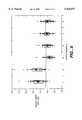
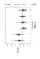
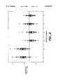
- FIGS. 5 and 6show Kelvin deep via 0.5 ⁇ m and 0.45 ⁇ m resistance measurements.
- FIGS. 7 and 8show Kelvin deep via/field 0.5 ⁇ m and 0.45 ⁇ m resistance measurements.
- wafer numbers 1 and 2denote wafers that were subject to the ozone dry stripping whereas wafer numbers 3-6 denote wafers that were subject to CF 4 and H 2 O. Wafers 3 and 4 were treated for 90 seconds and wafers 5 and 6 for 120 seconds. As is apparent, wafers dry stripped with the CF 4 and H 2 O ashing processes developed vias having resistances that were significantly lower than those subject to the ozone process.
Landscapes
- Engineering & Computer Science (AREA)
- Physics & Mathematics (AREA)
- General Physics & Mathematics (AREA)
- Computer Hardware Design (AREA)
- Condensed Matter Physics & Semiconductors (AREA)
- Manufacturing & Machinery (AREA)
- Microelectronics & Electronic Packaging (AREA)
- Power Engineering (AREA)
- Plasma & Fusion (AREA)
- Chemical & Material Sciences (AREA)
- Chemical Kinetics & Catalysis (AREA)
- General Chemical & Material Sciences (AREA)
- Drying Of Semiconductors (AREA)
- Internal Circuitry In Semiconductor Integrated Circuit Devices (AREA)
Abstract
Description
TABLE 1______________________________________StepsParameters 1 2 3 4 5 6 7 8 9______________________________________Press. Mt 90 10 10 10 10 10 10 10 90RF Top W 0 0 600 0 450 350 0 600 0RF Bot W 0 0 75 0 150 150 0 25 0Cl.sub.2sccm 0 0 0 50 50 50 0 0 0Bcl.sub.3 sccm 40 40 40 15 15 15 60 60 0SF.sub.6 sccm 40 40 40 0 0 0 45 45 0N.sub.2 sccm 10 10 10 0 0 0 12 12 0CHF.sub.3sccm 0 0 0 7 7 3 0 0 0He ClampT 0 3 3 8 8 8 3 3 0Time sec 10 15 25 20 100 70 20 85 10______________________________________
TABLE 2______________________________________StepsParameters 1 2 3 5 6______________________________________Paddle position DN UP UP DN DN (Down)Press. Mt 1200 1200 1200 0 0RF W 0 0 1000 0 0CF.sub.4sccm 0 80 80 0 0H.sub.2 O sccm 500 200 200 0 0Time sec 5 15 90 3 0______________________________________
Claims (11)
Priority Applications (1)
| Application Number | Priority Date | Filing Date | Title |
|---|---|---|---|
| US08/943,891US5925577A (en) | 1997-02-19 | 1997-10-03 | Method for forming via contact hole in a semiconductor device |
Applications Claiming Priority (2)
| Application Number | Priority Date | Filing Date | Title |
|---|---|---|---|
| US08/803,180US5851302A (en) | 1997-02-19 | 1997-02-19 | Method for dry etching sidewall polymer |
| US08/943,891US5925577A (en) | 1997-02-19 | 1997-10-03 | Method for forming via contact hole in a semiconductor device |
Related Parent Applications (1)
| Application Number | Title | Priority Date | Filing Date |
|---|---|---|---|
| US08/803,180Continuation-In-PartUS5851302A (en) | 1997-02-19 | 1997-02-19 | Method for dry etching sidewall polymer |
Publications (1)
| Publication Number | Publication Date |
|---|---|
| US5925577Atrue US5925577A (en) | 1999-07-20 |
Family
ID=46253721
Family Applications (1)
| Application Number | Title | Priority Date | Filing Date |
|---|---|---|---|
| US08/943,891Expired - LifetimeUS5925577A (en) | 1997-02-19 | 1997-10-03 | Method for forming via contact hole in a semiconductor device |
Country Status (1)
| Country | Link |
|---|---|
| US (1) | US5925577A (en) |
Cited By (29)
| Publication number | Priority date | Publication date | Assignee | Title |
|---|---|---|---|---|
| US6130169A (en)* | 1999-05-21 | 2000-10-10 | Advanced Micro Devices, Inc. | Efficient in-situ resist strip process for heavy polymer metal etch |
| US6130166A (en)* | 1999-02-01 | 2000-10-10 | Vlsi Technology, Inc. | Alternative plasma chemistry for enhanced photoresist removal |
| US6191086B1 (en)* | 1996-09-06 | 2001-02-20 | Arch Specialty Chemicals, Inc. | Cleaning composition and method for removing residues |
| WO2001031697A1 (en)* | 1999-10-27 | 2001-05-03 | Advanced Micro Devices, Inc. | Plasma treatment for polymer removal after via etch |
| US6232237B1 (en)* | 1997-12-12 | 2001-05-15 | Matsushita Electric Industrial Co., Ltd. | Method for fabricating semiconductor device |
| US6248179B1 (en)* | 1997-12-12 | 2001-06-19 | Stmicroelectronics S.A. | Method of removing polymeric material on a silicon water |
| WO2001054184A1 (en)* | 2000-01-19 | 2001-07-26 | Philips Semiconductors, Inc. | Method for removing residues with reduced etching of oxide |
| US6328905B1 (en)* | 1999-08-12 | 2001-12-11 | Advanced Micro Devices, Inc. | Residue removal by CO2 water rinse in conjunction with post metal etch plasma strip |
| US6352936B1 (en)* | 1998-02-27 | 2002-03-05 | Imec Vzw | Method for stripping ion implanted photoresist layer |
| US6355576B1 (en)* | 1999-04-26 | 2002-03-12 | Vlsi Technology Inc. | Method for cleaning integrated circuit bonding pads |
| US6372150B1 (en)* | 1998-12-18 | 2002-04-16 | Cypress Semiconductor Corp. | High vapor plasma strip methods and devices to enhance the reduction of organic residues over metal surfaces |
| US6406991B2 (en)* | 1999-12-27 | 2002-06-18 | Hoya Corporation | Method of manufacturing a contact element and a multi-layered wiring substrate, and wafer batch contact board |
| US20020104163A1 (en)* | 2001-01-25 | 2002-08-08 | Siemens Aktiengesellschaft | Support device for an imaging medical examination apparatus and method for the operation thereof |
| US6548230B1 (en)* | 1998-09-18 | 2003-04-15 | Taiwan Semiconductor Manufacturing Co., Ltd | Method for in-situ removal of photoresist and sidewall polymer |
| US6667244B1 (en)* | 2000-03-24 | 2003-12-23 | Gerald M. Cox | Method for etching sidewall polymer and other residues from the surface of semiconductor devices |
| US6693038B1 (en)* | 1999-02-05 | 2004-02-17 | Taiwan Semiconductor Manufacturing Company | Method for forming electrical contacts through multi-level dielectric layers by high density plasma etching |
| US6706623B1 (en)* | 1997-12-10 | 2004-03-16 | Texas Instruments Incorporated | Method and system for avoiding plasma etch damage |
| US6719917B2 (en)* | 2001-08-14 | 2004-04-13 | Samsung Electronics Co., Ltd. | Method of ashing semiconductor device having metal interconnection |
| US6734120B1 (en)* | 1999-02-19 | 2004-05-11 | Axcelis Technologies, Inc. | Method of photoresist ash residue removal |
| US20040241982A1 (en)* | 2003-05-27 | 2004-12-02 | Cho Jun Hee | Method of manufacturing semiconductor device |
| US20050153538A1 (en)* | 2004-01-09 | 2005-07-14 | Taiwan Semiconductor Manufacturing Co., Ltd. | Method for forming novel BARC open for precision critical dimension control |
| KR100500932B1 (en)* | 2001-09-28 | 2005-07-14 | 주식회사 하이닉스반도체 | Method of dry cleaning and photoresist strip after via contact etching |
| US20050196959A1 (en)* | 2002-04-26 | 2005-09-08 | Kazuykoshi Ueno | Semiconductor device and manufacturing process therefor as well as plating solution |
| US6943120B1 (en) | 2002-01-23 | 2005-09-13 | Taiwan Semiconductor Manufacturing Company, Ltd. | Method to improve via or contact hole profile using an in-situ polymer deposition and strip procedure |
| US20070181703A1 (en)* | 2006-02-07 | 2007-08-09 | Daryl Buchanan | System and method for producing and delivering vapor |
| US20100068836A1 (en)* | 2008-08-25 | 2010-03-18 | Youichi Yatagai | Method of measuring resistivity of sidewall of contact hole |
| US20130024019A1 (en)* | 2011-07-22 | 2013-01-24 | Taiwan Semiconductor Manufacturing Company, Ltd. | Apparatus and methods for end point determination in semiconductor processing |
| US9059250B2 (en) | 2012-02-17 | 2015-06-16 | International Business Machines Corporation | Lateral-dimension-reducing metallic hard mask etch |
| US11189484B2 (en)* | 2019-12-20 | 2021-11-30 | Micron Technology, Inc. | Semiconductor nitridation passivation |
Citations (14)
| Publication number | Priority date | Publication date | Assignee | Title |
|---|---|---|---|---|
| US4123841A (en)* | 1975-09-29 | 1978-11-07 | Sharp Kabushiki Kaisha | Electrochromic display device manufacture method |
| US4514254A (en)* | 1983-09-26 | 1985-04-30 | International Business Machines Corporation | Groundplane post-etch anodization |
| US4670091A (en)* | 1984-08-23 | 1987-06-02 | Fairchild Semiconductor Corporation | Process for forming vias on integrated circuits |
| US4983254A (en)* | 1989-01-10 | 1991-01-08 | Fujitsu Limited | Processing for stripping organic material |
| US5077598A (en)* | 1989-11-08 | 1991-12-31 | Hewlett-Packard Company | Strain relief flip-chip integrated circuit assembly with test fixturing |
| US5122225A (en)* | 1990-11-21 | 1992-06-16 | Texas Instruments Incorporated | Selective etch method |
| US5348619A (en)* | 1992-09-03 | 1994-09-20 | Texas Instruments Incorporated | Metal selective polymer removal |
| US5358602A (en)* | 1993-12-06 | 1994-10-25 | Enthone-Omi Inc. | Method for manufacture of printed circuit boards |
| US5451291A (en)* | 1992-03-31 | 1995-09-19 | Hyundai Electronics Industries Co., Ltd. | Method for forming a via contact hole of a semiconductor device |
| US5485304A (en)* | 1994-07-29 | 1996-01-16 | Texas Instruments, Inc. | Support posts for micro-mechanical devices |
| US5512507A (en)* | 1994-09-14 | 1996-04-30 | United Microelectronics Corporation | Process for post metal coding of a ROM, by gate etch |
| US5521104A (en)* | 1995-01-31 | 1996-05-28 | Texas Instruments Incorporated | Method for dry etching of post-processing interconnection metal on hybrid integrated circuits |
| US5526951A (en)* | 1994-09-30 | 1996-06-18 | Texas Instruments Incorporated | Fabrication method for digital micro-mirror devices using low temperature CVD |
| US5573971A (en)* | 1995-12-29 | 1996-11-12 | Cypress Semiconductor, Corporation | Planar antifuse and method of fabrication |
- 1997
- 1997-10-03USUS08/943,891patent/US5925577A/ennot_activeExpired - Lifetime
Patent Citations (15)
| Publication number | Priority date | Publication date | Assignee | Title |
|---|---|---|---|---|
| US4123841A (en)* | 1975-09-29 | 1978-11-07 | Sharp Kabushiki Kaisha | Electrochromic display device manufacture method |
| US4514254A (en)* | 1983-09-26 | 1985-04-30 | International Business Machines Corporation | Groundplane post-etch anodization |
| US4670091A (en)* | 1984-08-23 | 1987-06-02 | Fairchild Semiconductor Corporation | Process for forming vias on integrated circuits |
| US4983254A (en)* | 1989-01-10 | 1991-01-08 | Fujitsu Limited | Processing for stripping organic material |
| US5077598A (en)* | 1989-11-08 | 1991-12-31 | Hewlett-Packard Company | Strain relief flip-chip integrated circuit assembly with test fixturing |
| US5122225A (en)* | 1990-11-21 | 1992-06-16 | Texas Instruments Incorporated | Selective etch method |
| US5451291A (en)* | 1992-03-31 | 1995-09-19 | Hyundai Electronics Industries Co., Ltd. | Method for forming a via contact hole of a semiconductor device |
| US5348619A (en)* | 1992-09-03 | 1994-09-20 | Texas Instruments Incorporated | Metal selective polymer removal |
| US5358602A (en)* | 1993-12-06 | 1994-10-25 | Enthone-Omi Inc. | Method for manufacture of printed circuit boards |
| US5485304A (en)* | 1994-07-29 | 1996-01-16 | Texas Instruments, Inc. | Support posts for micro-mechanical devices |
| US5497262A (en)* | 1994-07-29 | 1996-03-05 | Texas Instruments Incorporated | Support posts for micro-mechanical devices |
| US5512507A (en)* | 1994-09-14 | 1996-04-30 | United Microelectronics Corporation | Process for post metal coding of a ROM, by gate etch |
| US5526951A (en)* | 1994-09-30 | 1996-06-18 | Texas Instruments Incorporated | Fabrication method for digital micro-mirror devices using low temperature CVD |
| US5521104A (en)* | 1995-01-31 | 1996-05-28 | Texas Instruments Incorporated | Method for dry etching of post-processing interconnection metal on hybrid integrated circuits |
| US5573971A (en)* | 1995-12-29 | 1996-11-12 | Cypress Semiconductor, Corporation | Planar antifuse and method of fabrication |
Cited By (37)
| Publication number | Priority date | Publication date | Assignee | Title |
|---|---|---|---|---|
| US6191086B1 (en)* | 1996-09-06 | 2001-02-20 | Arch Specialty Chemicals, Inc. | Cleaning composition and method for removing residues |
| US6706623B1 (en)* | 1997-12-10 | 2004-03-16 | Texas Instruments Incorporated | Method and system for avoiding plasma etch damage |
| US6232237B1 (en)* | 1997-12-12 | 2001-05-15 | Matsushita Electric Industrial Co., Ltd. | Method for fabricating semiconductor device |
| US6248179B1 (en)* | 1997-12-12 | 2001-06-19 | Stmicroelectronics S.A. | Method of removing polymeric material on a silicon water |
| US6352936B1 (en)* | 1998-02-27 | 2002-03-05 | Imec Vzw | Method for stripping ion implanted photoresist layer |
| US6548230B1 (en)* | 1998-09-18 | 2003-04-15 | Taiwan Semiconductor Manufacturing Co., Ltd | Method for in-situ removal of photoresist and sidewall polymer |
| US6372150B1 (en)* | 1998-12-18 | 2002-04-16 | Cypress Semiconductor Corp. | High vapor plasma strip methods and devices to enhance the reduction of organic residues over metal surfaces |
| US6130166A (en)* | 1999-02-01 | 2000-10-10 | Vlsi Technology, Inc. | Alternative plasma chemistry for enhanced photoresist removal |
| US6693038B1 (en)* | 1999-02-05 | 2004-02-17 | Taiwan Semiconductor Manufacturing Company | Method for forming electrical contacts through multi-level dielectric layers by high density plasma etching |
| US6734120B1 (en)* | 1999-02-19 | 2004-05-11 | Axcelis Technologies, Inc. | Method of photoresist ash residue removal |
| US6355576B1 (en)* | 1999-04-26 | 2002-03-12 | Vlsi Technology Inc. | Method for cleaning integrated circuit bonding pads |
| US6130169A (en)* | 1999-05-21 | 2000-10-10 | Advanced Micro Devices, Inc. | Efficient in-situ resist strip process for heavy polymer metal etch |
| US6328905B1 (en)* | 1999-08-12 | 2001-12-11 | Advanced Micro Devices, Inc. | Residue removal by CO2 water rinse in conjunction with post metal etch plasma strip |
| WO2001031697A1 (en)* | 1999-10-27 | 2001-05-03 | Advanced Micro Devices, Inc. | Plasma treatment for polymer removal after via etch |
| US6431182B1 (en) | 1999-10-27 | 2002-08-13 | Advanced Micro Devices, Inc. | Plasma treatment for polymer removal after via etch |
| US20020192939A1 (en)* | 1999-12-27 | 2002-12-19 | Hoya Corporation | Method of manufacturing a contract element and a multi-layered wiring substrate, and wafer batch contact board |
| US6713376B2 (en) | 1999-12-27 | 2004-03-30 | Hoya Corporation | Method of manufacturing a contract element and a multi-layered wiring substrate, and wafer batch contact board |
| US6406991B2 (en)* | 1999-12-27 | 2002-06-18 | Hoya Corporation | Method of manufacturing a contact element and a multi-layered wiring substrate, and wafer batch contact board |
| WO2001054184A1 (en)* | 2000-01-19 | 2001-07-26 | Philips Semiconductors, Inc. | Method for removing residues with reduced etching of oxide |
| US6667244B1 (en)* | 2000-03-24 | 2003-12-23 | Gerald M. Cox | Method for etching sidewall polymer and other residues from the surface of semiconductor devices |
| US20020104163A1 (en)* | 2001-01-25 | 2002-08-08 | Siemens Aktiengesellschaft | Support device for an imaging medical examination apparatus and method for the operation thereof |
| US6719917B2 (en)* | 2001-08-14 | 2004-04-13 | Samsung Electronics Co., Ltd. | Method of ashing semiconductor device having metal interconnection |
| KR100500932B1 (en)* | 2001-09-28 | 2005-07-14 | 주식회사 하이닉스반도체 | Method of dry cleaning and photoresist strip after via contact etching |
| US6943120B1 (en) | 2002-01-23 | 2005-09-13 | Taiwan Semiconductor Manufacturing Company, Ltd. | Method to improve via or contact hole profile using an in-situ polymer deposition and strip procedure |
| US20050196959A1 (en)* | 2002-04-26 | 2005-09-08 | Kazuykoshi Ueno | Semiconductor device and manufacturing process therefor as well as plating solution |
| US7821135B2 (en)* | 2002-04-26 | 2010-10-26 | Nec Electronics Corporation | Semiconductor device with improved stress migration resistance and manufacturing process therefor |
| US6887788B2 (en) | 2003-05-27 | 2005-05-03 | Hynix Semiconductor Inc. | Method of manufacturing semiconductor device |
| US20040241982A1 (en)* | 2003-05-27 | 2004-12-02 | Cho Jun Hee | Method of manufacturing semiconductor device |
| US20050153538A1 (en)* | 2004-01-09 | 2005-07-14 | Taiwan Semiconductor Manufacturing Co., Ltd. | Method for forming novel BARC open for precision critical dimension control |
| US7265056B2 (en) | 2004-01-09 | 2007-09-04 | Taiwan Semiconductor Manufacturing Company, Ltd. | Method for forming novel BARC open for precision critical dimension control |
| US20070181703A1 (en)* | 2006-02-07 | 2007-08-09 | Daryl Buchanan | System and method for producing and delivering vapor |
| US7680399B2 (en) | 2006-02-07 | 2010-03-16 | Brooks Instrument, Llc | System and method for producing and delivering vapor |
| US20100068836A1 (en)* | 2008-08-25 | 2010-03-18 | Youichi Yatagai | Method of measuring resistivity of sidewall of contact hole |
| US7923268B2 (en)* | 2008-08-25 | 2011-04-12 | Oki Semiconductor Co., Ltd. | Method of measuring resistivity of sidewall of contact hole |
| US20130024019A1 (en)* | 2011-07-22 | 2013-01-24 | Taiwan Semiconductor Manufacturing Company, Ltd. | Apparatus and methods for end point determination in semiconductor processing |
| US9059250B2 (en) | 2012-02-17 | 2015-06-16 | International Business Machines Corporation | Lateral-dimension-reducing metallic hard mask etch |
| US11189484B2 (en)* | 2019-12-20 | 2021-11-30 | Micron Technology, Inc. | Semiconductor nitridation passivation |
Similar Documents
| Publication | Publication Date | Title |
|---|---|---|
| US5925577A (en) | Method for forming via contact hole in a semiconductor device | |
| US5851302A (en) | Method for dry etching sidewall polymer | |
| US6440864B1 (en) | Substrate cleaning process | |
| US6352081B1 (en) | Method of cleaning a semiconductor device processing chamber after a copper etch process | |
| US6014979A (en) | Localizing cleaning plasma for semiconductor processing | |
| US6692903B2 (en) | Substrate cleaning apparatus and method | |
| KR101887723B1 (en) | Etch process for controlling pattern cd and integrity in multi-layer masks | |
| US6461974B1 (en) | High temperature tungsten etching process | |
| US5419805A (en) | Selective etching of refractory metal nitrides | |
| KR100523365B1 (en) | Methods and apparatus for removing photoresist mask defects in a plasma reactor | |
| KR20010033061A (en) | Method for high temperature etching of patterned layers using an organic mask stack | |
| JPH08172077A (en) | Method for improving plasma etching of vias | |
| JP2007221150A (en) | Method of cleaning and striping photoresist from semiconductor wafer surface | |
| WO2001009934A1 (en) | Sidewall polymer forming gas additives for etching processes | |
| US5792672A (en) | Photoresist strip method | |
| KR20070089082A (en) | Method for Controlling Corrosion of Substrates | |
| US6325861B1 (en) | Method for etching and cleaning a substrate | |
| JP2007129219A (en) | Etching process using c4f8 for silicon dioxide and cf4 for titanium nitride | |
| JP2005109492A (en) | Cleaning method for processing chamber | |
| JP2002531932A (en) | Photoresist stripping method and composition by dry method in semiconductor manufacturing method | |
| US6955177B1 (en) | Methods for post polysilicon etch photoresist and polymer removal with minimal gate oxide loss | |
| US6566269B1 (en) | Removal of post etch residuals on wafer surface | |
| JPH1098029A (en) | Processing method to etch organic anti-reflective coating from substrate | |
| WO2000024048A1 (en) | Method of etching patterned layers useful as masking during subsequent etching or for damascene structures | |
| JP2004517470A (en) | Method for removing etching residue generated in via formation step |
Legal Events
| Date | Code | Title | Description |
|---|---|---|---|
| AS | Assignment | Owner name:VLSI TECHNOLOGY, INC., CALIFORNIA Free format text:ASSIGNMENT OF ASSIGNORS INTEREST;ASSIGNOR:SOLIS, RAMIRO;REEL/FRAME:008836/0720 Effective date:19970930 | |
| FEPP | Fee payment procedure | Free format text:PAYOR NUMBER ASSIGNED (ORIGINAL EVENT CODE: ASPN); ENTITY STATUS OF PATENT OWNER: LARGE ENTITY | |
| STCF | Information on status: patent grant | Free format text:PATENTED CASE | |
| FEPP | Fee payment procedure | Free format text:PAYOR NUMBER ASSIGNED (ORIGINAL EVENT CODE: ASPN); ENTITY STATUS OF PATENT OWNER: LARGE ENTITY Free format text:PAYER NUMBER DE-ASSIGNED (ORIGINAL EVENT CODE: RMPN); ENTITY STATUS OF PATENT OWNER: LARGE ENTITY | |
| FPAY | Fee payment | Year of fee payment:4 | |
| AS | Assignment | Owner name:PHILIPS SEMICONDUCTORS VLSI INC., NEW YORK Free format text:CHANGE OF NAME;ASSIGNOR:VLSI TECHNOLOGY, INC.;REEL/FRAME:018635/0570 Effective date:19990702 Owner name:NXP B.V., NETHERLANDS Free format text:ASSIGNMENT OF ASSIGNORS INTEREST;ASSIGNOR:PHILIPS SEMICONDUCTORS INC.;REEL/FRAME:018645/0779 Effective date:20061130 | |
| FPAY | Fee payment | Year of fee payment:8 | |
| AS | Assignment | Owner name:PHILIPS SEMICONDUCTORS INC., NEW YORK Free format text:CHANGE OF NAME;ASSIGNOR:PHILIPS SEMICONDUCTORS VLSI INC.;REEL/FRAME:018668/0255 Effective date:19991220 | |
| AS | Assignment | Owner name:MORGAN STANLEY SENIOR FUNDING, INC., ENGLAND Free format text:SECURITY AGREEMENT;ASSIGNOR:NXP B.V.;REEL/FRAME:018806/0201 Effective date:20061201 | |
| FPAY | Fee payment | Year of fee payment:12 | |
| AS | Assignment | Owner name:NXP B.V., NETHERLANDS Free format text:TERMINATION AND RELEASE OF SECURITY INTEREST IN PATENT RIGHTS;ASSIGNOR:MORGAN STANLEY SENIOR FUNDING, INC.;REEL/FRAME:037459/0140 Effective date:20160105 | |
| AS | Assignment | Owner name:UNITED MICROELECTRONICS CORP., TAIWAN Free format text:ASSIGNMENT OF ASSIGNORS INTEREST;ASSIGNOR:NXP B.V.;REEL/FRAME:037973/0107 Effective date:20151004 | |
| AS | Assignment | Owner name:NXP B.V., NETHERLANDS Free format text:RELEASE BY SECURED PARTY;ASSIGNOR:MORGAN STANLEY SENIOR FUNDING, INC;REEL/FRAME:050315/0443 Effective date:20190903 |