US5923594A - Method and apparatus for coupling data from a memory device using a single ended read data path - Google Patents
Method and apparatus for coupling data from a memory device using a single ended read data pathDownload PDFInfo
- Publication number
- US5923594A US5923594AUS09/024,367US2436798AUS5923594AUS 5923594 AUS5923594 AUS 5923594AUS 2436798 AUS2436798 AUS 2436798AUS 5923594 AUS5923594 AUS 5923594A
- Authority
- US
- United States
- Prior art keywords
- data
- coupled
- sense amplifier
- lines
- output
- Prior art date
- Legal status (The legal status is an assumption and is not a legal conclusion. Google has not performed a legal analysis and makes no representation as to the accuracy of the status listed.)
- Expired - Lifetime
Links
Images


Classifications
- G—PHYSICS
- G11—INFORMATION STORAGE
- G11C—STATIC STORES
- G11C7/00—Arrangements for writing information into, or reading information out from, a digital store
- G11C7/10—Input/output [I/O] data interface arrangements, e.g. I/O data control circuits, I/O data buffers
- G11C7/1051—Data output circuits, e.g. read-out amplifiers, data output buffers, data output registers, data output level conversion circuits
- G11C7/1069—I/O lines read out arrangements
- G—PHYSICS
- G11—INFORMATION STORAGE
- G11C—STATIC STORES
- G11C7/00—Arrangements for writing information into, or reading information out from, a digital store
- G11C7/10—Input/output [I/O] data interface arrangements, e.g. I/O data control circuits, I/O data buffers
- G11C7/1006—Data managing, e.g. manipulating data before writing or reading out, data bus switches or control circuits therefor
- G—PHYSICS
- G11—INFORMATION STORAGE
- G11C—STATIC STORES
- G11C7/00—Arrangements for writing information into, or reading information out from, a digital store
- G11C7/10—Input/output [I/O] data interface arrangements, e.g. I/O data control circuits, I/O data buffers
- G11C7/1051—Data output circuits, e.g. read-out amplifiers, data output buffers, data output registers, data output level conversion circuits
- G—PHYSICS
- G11—INFORMATION STORAGE
- G11C—STATIC STORES
- G11C2207/00—Indexing scheme relating to arrangements for writing information into, or reading information out from, a digital store
- G11C2207/10—Aspects relating to interfaces of memory device to external buses
- G11C2207/104—Embedded memory devices, e.g. memories with a processing device on the same die or ASIC memory designs
Definitions
- the inventionrelates generally to integrated circuit memory devices, and more particularly, to a read data path in a memory device.
- Modern integrated circuit memory devicesare comprised of a large number of components and conductive connections arranged on a surface of a silicon chip.
- the capacity of a memory device to store datais governed by the number of components which may be arranged on the silicon chip.
- the number of componentsis limited by the physical size or area of the surface of the silicon chip and the density of the components is limited by parasitic electrical effects which occur between proximate components. It is therefore desirable to minimize the number of components of the memory device to maximize the capacity of the memory device to store data.
- FIG. 1A conventional memory device is illustrated in FIG. 1.
- the memory deviceis a synchronous dynamic random access memory (“SDRAM") 10 which includes an address register 12 that receives either a row address or a column address on an address bus 14.
- the address bus 14is generally coupled to a memory controller (not shown in FIG. 1).
- a row addressis initially received by the address register 12 and applied to a row address multiplexer 18.
- the row address multiplexer 18couples the row address to a number of components associated with either of two memory bank arrays 20 and 22 depending upon the state of a bank address bit forming part of the row address.
- the arrays 20 and 22are comprised of memory cells arranged in rows and columns.
- each of the arrays 20 and 22Associated with each of the arrays 20 and 22 is a respective row address latch 26, which stores the row address, and a row decoder 28, which applies various signals to its respective array 20 or 22 as a function of the stored row address.
- the row address multiplexer 18also couples row addresses to the row address latches 26 for the purpose of refreshing the memory cells in the arrays 20 and 22.
- the row addressesare generated for refresh purposes by a refresh counter 30 that is controlled by a refresh controller 32.
- a column addressis applied to the address register 12.
- the address register 12couples the column address to a column address latch 40.
- the column addressis either coupled through a burst counter 42 to a column address buffer 44, or to the burst counter 42, which applies a sequence of column addresses to the column address buffer 44 starting at the column address output by the address register 12.
- the column address buffer 44applies a column address to a column decoder 48, which applies various column signals to respective sense amplifiers and associated column circuits 50 and 52 for the respective arrays 20 and 22.
- Data to be read from one of the arrays 20 or 22are coupled from the arrays 20 or 22, respectively, to a data bus 58 through the column circuit 50 or 52, respectively, and a read data path that includes a data output register 56.
- Data to be written to one of the arrays 20 or 22are coupled from the data bus 58 through a write data path, including a data input register 60, to one of the column circuits 50 or 52 where they are transferred to one of the arrays 20 or 22, respectively.
- a mask register 64may be used to selectively alter the flow of data into and out of the column circuits 50 and 52 by, for example, selectively masking data to be read from the arrays 20 and 22.
- the above-described operation of the SDRAM 10is controlled by a command decoder 68 responsive to high level command signals received on a control bus 70.
- These high level command signalswhich are typically generated by the memory controller, are a clock enable signal CKE*, a clock signal CLK, a chip select signal CS*, a write enable signal WE*, a row address strobe signal RAS*, and a column address strobe signal CAS*, where the "*" designates the signal as active low.
- the command decoder 68generates a sequence of command signals responsive to the high level command signals to carry out a function (e.g., a read or a write) designated by each of the high level command signals.
- a functione.g., a read or a write
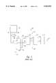
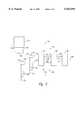
- read dataare coupled from one of the arrays 20 and 22 to the data bus 58 through a read data path that is shown in greater detail in FIG. 2.
- the read data path 80is subsumed in the column circuits 50 and 52 and the data output register 56 shown in FIG. 1.
- the read data path 80begins in one of the columns in the array 20.
- the columnincludes a complementary pair of digit lines 84 and 86 coupled to the memory cells in the column.
- a sense amplifier 88connected between the digit lines 84 and 86 amplifies a differential data signal on the digit lines 84 and 86 in a well-known manner.
- the differential data signalindicates the presence of a "1" or a "0" in an enabled memory cell in the column.
- the digit lines 84 and 86are selectively coupled to a complementary pair of I/O lines 90 and 92 by well known column addressing circuitry, which is not shown in FIG. 2 for purposes of brevity.
- the I/O lines 90 and 92are also selectively coupled to the digit lines for a large number of other columns, but these other digit lines have been omitted for purposes of clarity.
- the I/O lines 90 and 92are selectively coupled to a complementary pair of data lines 94 and 96 by first and second pass gates 98 and 100.
- the pass gates 98 and 100are located in a multiplexer (not shown) that selectively couples the pair of data lines 94 and 96 to at least one other complementary pair of I/O lines (not shown).
- a conductive state of each of the pass gates 98 and 100is controlled by a bank address signal derived from the bank address bit, which is applied to a control line 102 for the pass gate 98 and to a control line 104 for the pass gate 100.
- Each of the pass gates 98 and 100receives the bank address signal at a first terminal, and an inverted bank address signal at a second terminal, which is received from one of two inverters 106 and 108, respectively.
- the differential data signalis coupled from the digit lines 84 and 86 through the I/O lines 90 and 92 to the data lines 94 and 96.
- the data lines 94 and 96are coupled, respectively, to complementary inputs of a DC sense amplifier 110.
- the DC sense amplifier 110is a high speed, high gain differential amplifier that amplifies the differential data signal on the data lines 94 and 96 to full CMOS voltage levels.
- An amplified differential data signalis generated by the DC sense amplifier 110 at complementary outputs and provided to a complementary pair of primary data path lines 112 and 114.
- the primary data path lines 112 and 114provide the amplified differential data signal to a complementary pair of inputs of a multiplexer 116.
- the multiplexer 116receives amplified differential data signals from other DC sense amplifiers through alternate primary data path lines 118 and 120 and provides a selected amplified differential data signal from complementary outputs to a complementary pair of secondary data path lines 122 and 124.
- the secondary data path lines 122 and 124are connected to a complementary pair of inputs in a data output buffer 126, which provides a data signal to a data bus terminal 128 based on the amplified differential data signal.
- the components required to support a single array in a memory deviceare numerous and occupy a substantial amount of a silicon chip. It is therefore advantageous to reduce the number of these components required for each array and thereby increase the capacity of the memory device to store data.
- a method and apparatus for coupling data from a memory device using a single ended read data pathincludes an array of memory cells arranged in rows and columns, each column having a complementary pair of digit lines, a sense amplifier coupled to the pair of digit lines, and at least one complementary pair of data lines coupled respectively to a selected one of the pairs of digit lines.
- the memory devicealso includes a DC sense amplifier having a complementary pair of inputs coupled to the pair of data lines and an output. The DC sense amplifier is structured to generate an amplified signal at the output based on a differential data signal received from the pair of digit lines via the pair of data lines.
- a data output circuithas an input coupled to the output of the DC sense amplifier by a single conductive path to receive the amplified signal.
- the data output circuitis structured to provide a data signal to a data output terminal based on the amplified signal.
- the digit linesare coupled to the data lines through a pair of pass gates.
- a complementary pair of I/O linesis coupled, respectively, between the digit lines and the pass gates.
- the DC sense amplifieris a differential amplifier having a second output coupled to a capacitor and is structured to receive the differential data signal and generate an amplified differential data signal from the first and second outputs.
- the memory devicemay also include a multiplexer coupled between the DC sense amplifier and the data output circuit coupled to receive amplified signals from several DC sense amplifiers and being structured to select an appropriate amplified signal to be transmitted to the data output circuit.
- FIG. 1is a block diagram of a memory device according to the prior art.
- FIG. 2is a block diagram of a differential read data path according to the prior art.
- FIG. 3is a block diagram of a single ended read data path according to one embodiment of the present invention.
- FIG. 4is a block diagram of a single ended read data path without a multiplexer according to another embodiment of the present invention.
- FIG. 5is a block diagram of elements of a memory device including the single ended read data path of FIG. 3 showing approximate distances between the elements on a surface of a semiconductor chip.
- FIG. 6is a block diagram of a computer system including the single ended read data path of FIG. 3 or FIG. 4.
- a single ended read data path 140is shown in FIG. 3.
- the single ended read data path 140like the read data path 80 of FIG. 2, includes a memory bank array 142, a complementary pair of digit lines 144 and 146, a sense amplifier 148 connected between the digit lines 144 and 146, a complementary pair of I/O lines 150 and 152 coupled to the digit lines 144 and 146 and a complementary pair of data lines 154 and 156 coupled to the I/O lines 150 and 152 by pass gates 158 and 160.
- the pass gates 158 and 160are located in a multiplexer (not shown).
- a DC sense amplifier 174includes input terminals coupled to the data lines 154 and 156.
- the read data path 140begins to deviate from the read data path 80 at the DC sense amplifier 174. More specifically, although the DC sense amplifier 174 includes a first complementary output 176 and a second complementary output 178, the second complementary output 178 is preferably connected to a ground voltage reference through a capacitor 180.
- a single, primary data path line 182is connected between the first complementary output 176 of the DC sense amplifier 174 and an input 184 of a multiplexer 186.
- the multiplexer 186receives signals from other DC sense amplifiers through alternate primary data path lines 188 and 190.
- the multiplexer 186has a single output 191 which is connected by a single, secondary data path line 192 to an input 194 of a data output buffer 196.
- the data output buffer 196has an output 198 connected to a data bus terminal 200.
- the capacitor 180is preferably selected to be approximately equivalent to the line capacitance of the primary data path line 182 in order to provide a voltage balance between the first and second complementary outputs 176 and 178 of the DC sense amplifier 174.
- the single ended read data path 140provides the advantage of having a single primary data path line 182 carrying data from the memory cell between the DC sense amplifier 174 and the multiplexer 186, and a single secondary data path line 192 carrying the data between the multiplexer 186 and the data output buffer 196.
- the single ended read data path 140eliminates a complementary primary data path line between the DC sense amplifier 174 and the multiplexer 186, and a complementary secondary data path line between the multiplexer 186 and the data output buffer 196, thereby reducing the number of conductive connections, which reduces the amount of silicon necessary to support a memory device with the single ended read data path 140.
- the elimination of conductive pathsmay also reduce the amount of power consumed by the memory device.
- a single ended read data path 220begins in a column in a memory bank array 222 that is coupled through a pair of digit lines 224 and 226 to a sense amplifier 228 as explained above with reference to FIGS. 1-3.
- the digit lines 224 and 226are selectively coupled to a complementary pair of I/O lines 230 and 232, and the I/O lines 230 and 232 are selectively coupled to a complementary pair of data lines 234 and 236 by two pass gates 238 and 240.
- the pass gates 238 and 240are controlled by a bank address signal applied to respective control lines 242 and 244 directly and through respective inverters 246 and 248.
- a differential data signalis coupled from the digit lines 224 and 226 through the I/O lines 230 and 232 to the data lines 234 and 236.
- the data lines 234 and 236are coupled, respectively, to a first complementary input 250 and a second complementary input 252 of a DC sense amplifier 254.
- a first differential output 256 of the DC sense amplifier 254is coupled to a capacitor 260.
- FIG. 4differs from the embodiment of FIG. 3 by omitting the multiplexer 186 of FIG. 3. Instead, a single data path line 262 is connected between a second complementary output 258 of the DC sense amplifier 254 and an input 264 of a data output buffer 266.
- the data output buffer 266has an output 268 connected to a data bus terminal 270.
- FIG. 5is a block diagram of several elements of an SDRAM 276 as they are arranged on a surface of a semiconductor chip according to another embodiment of the invention.
- the SDRAM 276includes a single ended read data path similar to the one shown in FIG. 3.
- the blocks in FIG. 5are shown spaced to indicate relative distances between elements of the SDRAM 276 on the surface of the semiconductor chip.
- Two memory bank arrays 278 and 280are located in a center of the semiconductor chip.
- the arrays 278 and 280are comprised of memory cells arranged in rows and columns.
- Each of the arrays 278 and 280includes a respective set of pairs of digit lines for each column, a sense amplifier coupled to each pair of digit lines, and a set of multiplexers located near the bottom of each of the arrays 278 and 280.
- Each of the arrays 278 and 280is coupled to a respective data path circuit 282 and 284 through a plurality of respective data lines which are not shown for purposes of clarity.
- the data path circuits 282 and 284contain respective DC sense amplifiers coupled to receive the data lines and respective multiplexers coupled to receive a single data path line for every pair of data lines received by the DC sense amplifiers.
- An output circuit 286includes a plurality of data output buffers and data bus terminals, which are structured to be coupled to a data bus. The data bus terminals in the output circuit 286 are arranged in a horseshoe pattern around the sides and bottom of the semiconductor chip containing the SDRAM 276.
- Each multiplexer in the data path circuits 282 and 284is connected to a respective data output buffer in the output circuit 286 through a single data path line.
- the data path linesare not shown for purposes of clarity.
- the data path circuits 282 and 284are located closer to the arrays 278 and 280 than to the output circuit 286.
- logic circuitry in the SDRAM 276such as row address and column address circuitry, read/write control circuitry, and associated multiplexers are arranged on the surface of the semiconductor chip between the arrays 278 and 280 and the output circuit 286 in a manner that is also not shown. This additional logic circuitry is embedded between the arrays 278 and 280 and the output circuit 286 in a very dense and intricate fashion.
- One of the significant advantages of the inventionis that the employment of a single data path line between each of the DC sense amplifiers and the multiplexers in the data path circuitry 282 and 284 and respective data output buffers in the output circuit 286 eliminates one-half of the multiplexers and read/write control circuitry that would be necessary to support a fully differential data path between each of the DC sense amplifiers and the data output buffers. As a consequence, mutual parasitic effects between the circuit elements in the SDRAM 276 are reduced and more circuitry may be arranged on a smaller surface area of the semiconductor chip.
- FIG. 6is a block diagram of a computer system 300, which includes an SDRAM 301 having a single ended read data path similar to those shown in FIGS. 3 and 4.
- the computer system 300includes a processor 302 for performing various computing functions, such as executing specific software to perform specific calculations or tasks.
- the processor 302includes a processor bus 304 that includes an address bus, a control bus, and a data bus.
- the computer system 300includes one or more input devices 314, such as a keyboard or a mouse, coupled to the processor 302 to allow an operator to interface with the computer system 300.
- the computer system 300also includes one or more output devices 316 coupled to the processor 302, such as a printer or a video terminal.
- One or more data storage devices 318may also be coupled to the processor 302 to allow the processor 302 to store data or retrieve data from internal or external storage media (not shown). Examples of typical storage devices 318 include hard and floppy disks, tape cassettes, and compact disk read-only memories (CD-ROMs).
- the processor 302is also coupled to a cache memory 326, which is a static random access memory (“SRAM"), and to the SDRAM 301 through a memory controller 330.
- the memory controller 330includes a control bus 332 and an address bus 334 which are coupled to the SDRAM 301.
- a data bus 336is coupled between the SDRAM 301 and the processor bus 304.
Landscapes
- Dram (AREA)
Abstract
Description
Claims (6)
Priority Applications (2)
| Application Number | Priority Date | Filing Date | Title |
|---|---|---|---|
| US09/024,367US5923594A (en) | 1998-02-17 | 1998-02-17 | Method and apparatus for coupling data from a memory device using a single ended read data path |
| US09/336,391US6091646A (en) | 1998-02-17 | 1999-06-18 | Method and apparatus for coupling data from a memory device using a single ended read data path |
Applications Claiming Priority (1)
| Application Number | Priority Date | Filing Date | Title |
|---|---|---|---|
| US09/024,367US5923594A (en) | 1998-02-17 | 1998-02-17 | Method and apparatus for coupling data from a memory device using a single ended read data path |
Related Child Applications (1)
| Application Number | Title | Priority Date | Filing Date |
|---|---|---|---|
| US09/336,391ContinuationUS6091646A (en) | 1998-02-17 | 1999-06-18 | Method and apparatus for coupling data from a memory device using a single ended read data path |
Publications (1)
| Publication Number | Publication Date |
|---|---|
| US5923594Atrue US5923594A (en) | 1999-07-13 |
Family
ID=21820226
Family Applications (2)
| Application Number | Title | Priority Date | Filing Date |
|---|---|---|---|
| US09/024,367Expired - LifetimeUS5923594A (en) | 1998-02-17 | 1998-02-17 | Method and apparatus for coupling data from a memory device using a single ended read data path |
| US09/336,391Expired - LifetimeUS6091646A (en) | 1998-02-17 | 1999-06-18 | Method and apparatus for coupling data from a memory device using a single ended read data path |
Family Applications After (1)
| Application Number | Title | Priority Date | Filing Date |
|---|---|---|---|
| US09/336,391Expired - LifetimeUS6091646A (en) | 1998-02-17 | 1999-06-18 | Method and apparatus for coupling data from a memory device using a single ended read data path |
Country Status (1)
| Country | Link |
|---|---|
| US (2) | US5923594A (en) |
Cited By (9)
| Publication number | Priority date | Publication date | Assignee | Title |
|---|---|---|---|---|
| US6101132A (en)* | 1999-02-03 | 2000-08-08 | Xilinx, Inc. | Block RAM with reset |
| US6256255B1 (en) | 1997-03-11 | 2001-07-03 | Micron Technology, Inc. | Multi-bank memory input/output line selection |
| US6272608B1 (en) | 1997-07-10 | 2001-08-07 | Micron Technology, Inc. | Method and apparatus for synchronous data transfers in a memory device with lookahead logic for detecting latency intervals |
| US6282127B1 (en) | 1999-02-03 | 2001-08-28 | Xilinx, Inc. | Block RAM with reset to user selected value |
| US6295618B1 (en)* | 1998-08-25 | 2001-09-25 | Micron Technology, Inc. | Method and apparatus for data compression in memory devices |
| US6405280B1 (en) | 1998-06-05 | 2002-06-11 | Micron Technology, Inc. | Packet-oriented synchronous DRAM interface supporting a plurality of orderings for data block transfers within a burst sequence |
| US6411553B1 (en)* | 2000-08-31 | 2002-06-25 | Micron Technology, Inc. | Single ended data bus equilibration scheme |
| US6430099B1 (en)* | 2001-05-11 | 2002-08-06 | Broadcom Corporation | Method and apparatus to conditionally precharge a partitioned read-only memory with shared wordlines for low power operation |
| US6519719B1 (en) | 1997-06-13 | 2003-02-11 | Micron Technology, Inc. | Method and apparatus for transferring test data from a memory array |
Families Citing this family (1)
| Publication number | Priority date | Publication date | Assignee | Title |
|---|---|---|---|---|
| US7463761B2 (en)* | 2004-05-27 | 2008-12-09 | Aperio Technologies, Inc. | Systems and methods for creating and viewing three dimensional virtual slides |
Citations (65)
| Publication number | Priority date | Publication date | Assignee | Title |
|---|---|---|---|---|
| US4096402A (en)* | 1975-12-29 | 1978-06-20 | Mostek Corporation | MOSFET buffer for TTL logic input and method of operation |
| US4404474A (en)* | 1981-02-06 | 1983-09-13 | Rca Corporation | Active load pulse generating circuit |
| US4611337A (en)* | 1983-08-29 | 1986-09-09 | General Electric Company | Minimal logic synchronous up/down counter implementations for CMOS |
| US4638187A (en)* | 1985-10-01 | 1987-01-20 | Vtc Incorporated | CMOS output buffer providing high drive current with minimum output signal distortion |
| US4789796A (en)* | 1985-12-23 | 1988-12-06 | U.S. Philips Corporation | Output buffer having sequentially-switched output |
| JPH02112317A (en)* | 1988-10-20 | 1990-04-25 | Nec Corp | Output circuit |
| US4958088A (en)* | 1989-06-19 | 1990-09-18 | Micron Technology, Inc. | Low power three-stage CMOS input buffer with controlled switching |
| US4984204A (en)* | 1988-01-28 | 1991-01-08 | Hitachi, Ltd. | High speed sensor system using a level shift circuit |
| EP0450871A2 (en)* | 1990-03-30 | 1991-10-09 | Xerox Corporation | Interfaces for transmission lines |
| US5111435A (en)* | 1987-03-31 | 1992-05-05 | Kabushiki Kaisha Toshiba | Bipolar-CMOS semiconductor memory device |
| JPH04135311A (en)* | 1990-09-27 | 1992-05-08 | Nec Corp | Semiconductor integrated circuit |
| US5122690A (en)* | 1990-10-16 | 1992-06-16 | General Electric Company | Interface circuits including driver circuits with switching noise reduction |
| US5128560A (en)* | 1991-03-22 | 1992-07-07 | Micron Technology, Inc. | Boosted supply output driver circuit for driving an all N-channel output stage |
| US5128563A (en)* | 1990-11-28 | 1992-07-07 | Micron Technology, Inc. | CMOS bootstrapped output driver method and circuit |
| US5134311A (en)* | 1990-06-07 | 1992-07-28 | International Business Machines Corporation | Self-adjusting impedance matching driver |
| US5150186A (en)* | 1991-03-06 | 1992-09-22 | Micron Technology, Inc. | CMOS output pull-up driver |
| US5165046A (en)* | 1989-11-06 | 1992-11-17 | Micron Technology, Inc. | High speed CMOS driver circuit |
| US5179298A (en)* | 1990-01-17 | 1993-01-12 | Matsushita Electric Industrial Co., Ltd. | CMOS buffer circuit which is not influenced by bounce noise |
| US5194765A (en)* | 1991-06-28 | 1993-03-16 | At&T Bell Laboratories | Digitally controlled element sizing |
| JPH05136664A (en)* | 1991-08-14 | 1993-06-01 | Advantest Corp | Variable delay circuit |
| US5220208A (en)* | 1991-04-29 | 1993-06-15 | Texas Instruments Incorporated | Circuitry and method for controlling current in an electronic circuit |
| US5239206A (en)* | 1990-03-06 | 1993-08-24 | Advanced Micro Devices, Inc. | Synchronous circuit with clock skew compensating function and circuits utilizing same |
| US5254883A (en)* | 1992-04-22 | 1993-10-19 | Rambus, Inc. | Electrical current source circuitry for a bus |
| JPH05282868A (en)* | 1992-04-02 | 1993-10-29 | Fujitsu Ltd | Semiconductor memory device |
| US5274276A (en)* | 1992-06-26 | 1993-12-28 | Micron Technology, Inc. | Output driver circuit comprising a programmable circuit for determining the potential at the output node and the method of implementing the circuit |
| US5276642A (en)* | 1991-07-15 | 1994-01-04 | Micron Technology, Inc. | Method for performing a split read/write operation in a dynamic random access memory |
| US5278460A (en)* | 1992-04-07 | 1994-01-11 | Micron Technology, Inc. | Voltage compensating CMOS input buffer |
| US5281865A (en)* | 1990-11-28 | 1994-01-25 | Hitachi, Ltd. | Flip-flop circuit |
| US5311481A (en)* | 1992-12-17 | 1994-05-10 | Micron Technology, Inc. | Wordline driver circuit having a directly gated pull-down device |
| US5321368A (en)* | 1992-02-27 | 1994-06-14 | Siemens Aktiengesellschaft | Synchronized, digital sequential circuit |
| US5347177A (en)* | 1993-01-14 | 1994-09-13 | Lipp Robert J | System for interconnecting VLSI circuits with transmission line characteristics |
| US5347179A (en)* | 1993-04-15 | 1994-09-13 | Micron Semiconductor, Inc. | Inverting output driver circuit for reducing electron injection into the substrate |
| US5390308A (en)* | 1992-04-15 | 1995-02-14 | Rambus, Inc. | Method and apparatus for address mapping of dynamic random access memory |
| US5400283A (en)* | 1993-12-13 | 1995-03-21 | Micron Semiconductor, Inc. | RAM row decode circuitry that utilizes a precharge circuit that is deactivated by a feedback from an activated word line driver |
| EP0655741A2 (en)* | 1993-11-29 | 1995-05-31 | Kabushiki Kaisha Toshiba | Memory device and serial-parallel data transform circuit |
| US5438545A (en)* | 1993-12-21 | 1995-08-01 | Goldstar Electron Co., Ltd. | Data output buffer of semiconductor memory device for preventing noises |
| US5440260A (en)* | 1991-08-14 | 1995-08-08 | Advantest Corporation | Variable delay circuit |
| US5457407A (en)* | 1994-07-06 | 1995-10-10 | Sony Electronics Inc. | Binary weighted reference circuit for a variable impedance output buffer |
| EP0680049A2 (en)* | 1994-04-29 | 1995-11-02 | Mosaid Technologies Incorporated | Synchronizer |
| US5473575A (en)* | 1990-04-18 | 1995-12-05 | Rambus, Inc. | Integrated circuit I/O using a high performance bus interface |
| US5475642A (en)* | 1992-06-23 | 1995-12-12 | Taylor; David L. | Dynamic random access memory with bit line preamp/driver |
| EP0692872A2 (en)* | 1994-07-11 | 1996-01-17 | International Business Machines Corporation | Scannable master slave latch actuated by single phase clock |
| US5497127A (en)* | 1994-12-14 | 1996-03-05 | David Sarnoff Research Center, Inc. | Wide frequency range CMOS relaxation oscillator with variable hysteresis |
| US5498990A (en)* | 1991-11-05 | 1996-03-12 | Monolithic System Technology, Inc. | Reduced CMOS-swing clamping circuit for bus lines |
| US5506814A (en)* | 1993-05-28 | 1996-04-09 | Micron Technology, Inc. | Video random access memory device and method implementing independent two WE nibble control |
| US5508638A (en)* | 1994-02-24 | 1996-04-16 | Micron Technology, Inc. | Low current redundancy fuse assembly |
| US5568077A (en)* | 1994-11-07 | 1996-10-22 | Mitsubishi Denki Kabushiki Kaisha | Latch circuit |
| US5576645A (en)* | 1995-06-05 | 1996-11-19 | Hughes Aircraft Company | Sample and hold flip-flop for CMOS logic |
| US5578941A (en)* | 1995-08-23 | 1996-11-26 | Micron Technology, Inc. | Voltage compensating CMOS input buffer circuit |
| US5581197A (en)* | 1995-05-31 | 1996-12-03 | Hewlett-Packard Co. | Method of programming a desired source resistance for a driver stage |
| US5590073A (en)* | 1993-11-30 | 1996-12-31 | Sony Corporation | Random access memory having flash memory |
| US5619473A (en)* | 1994-08-23 | 1997-04-08 | Sharp Kabushiki Kaisha | Semiconductor memory device with dual address memory read amplifiers |
| US5621690A (en)* | 1995-04-28 | 1997-04-15 | Intel Corporation | Nonvolatile memory blocking architecture and redundancy |
| US5627780A (en)* | 1994-08-26 | 1997-05-06 | Sgs-Thomson Microelectronics Limited | Testing a non-volatile memory |
| US5627791A (en)* | 1996-02-16 | 1997-05-06 | Micron Technology, Inc. | Multiple bank memory with auto refresh to specified bank |
| US5631872A (en)* | 1995-08-14 | 1997-05-20 | Nec Corporation | Low power consumption semiconductor dynamic random access memory device by reusing residual electric charge on bit line pairs |
| US5636163A (en)* | 1986-07-30 | 1997-06-03 | Mitsubishi Denki Kabushiki Kaisha | Random access memory with a plurality amplifier groups for reading and writing in normal and test modes |
| US5636173A (en)* | 1995-06-07 | 1997-06-03 | Micron Technology, Inc. | Auto-precharge during bank selection |
| US5636174A (en)* | 1996-01-11 | 1997-06-03 | Cirrus Logic, Inc. | Fast cycle time-low latency dynamic random access memories and systems and methods using the same |
| US5638335A (en)* | 1995-05-22 | 1997-06-10 | Hitachi, Ltd. | Semiconductor device |
| US5655105A (en)* | 1995-06-30 | 1997-08-05 | Micron Technology, Inc. | Method and apparatus for multiple latency synchronous pipelined dynamic random access memory |
| US5668763A (en)* | 1996-02-26 | 1997-09-16 | Fujitsu Limited | Semiconductor memory for increasing the number of half good memories by selecting and using good memory blocks |
| US5694065A (en)* | 1994-08-16 | 1997-12-02 | Burr-Brown Corporation | Switching control circuitry for low noise CMOS inverter |
| US5737276A (en)* | 1995-09-11 | 1998-04-07 | Samsung Electronics Co., Ltd. | Memory device with fast extended data out (EDO) mode and methods of operation therefor |
| US5831929A (en)* | 1997-04-04 | 1998-11-03 | Micron Technology, Inc. | Memory device with staggered data paths |
Family Cites Families (19)
| Publication number | Priority date | Publication date | Assignee | Title |
|---|---|---|---|---|
| US35934A (en)* | 1862-07-22 | Improvement in bonnet-frames | ||
| JPS62293599A (en)* | 1986-06-13 | 1987-12-21 | Hitachi Ltd | Semiconductor storage device |
| US4884270A (en)* | 1986-12-11 | 1989-11-28 | Texas Instruments Incorporated | Easily cascadable and testable cache memory |
| US5170074A (en)* | 1990-03-13 | 1992-12-08 | Nec Corporation | Master-slave clocked flip-flop circuit |
| US5471591A (en)* | 1990-06-29 | 1995-11-28 | Digital Equipment Corporation | Combined write-operand queue and read-after-write dependency scoreboard |
| JP3256554B2 (en)* | 1991-02-25 | 2002-02-12 | 株式会社日立製作所 | Semiconductor integrated circuit device |
| EP0579862A1 (en)* | 1992-07-24 | 1994-01-26 | Siemens Aktiengesellschaft | Integrated semi-conductor memory device |
| US5440506A (en)* | 1992-08-14 | 1995-08-08 | Harris Corporation | Semiconductor ROM device and method |
| US5467473A (en)* | 1993-01-08 | 1995-11-14 | International Business Machines Corporation | Out of order instruction load and store comparison |
| JPH06290582A (en) | 1993-04-02 | 1994-10-18 | Nec Corp | Semiconductor memory |
| US5383157A (en)* | 1993-08-06 | 1995-01-17 | Cypress Semiconductor Corporation | Parallel TESTMODE |
| JP3304531B2 (en)* | 1993-08-24 | 2002-07-22 | 富士通株式会社 | Semiconductor storage device |
| JPH07130185A (en)* | 1993-09-13 | 1995-05-19 | Mitsubishi Electric Corp | Semiconductor memory device |
| US5847577A (en)* | 1995-02-24 | 1998-12-08 | Xilinx, Inc. | DRAM memory cell for programmable logic devices |
| US5764963A (en)* | 1995-07-07 | 1998-06-09 | Rambus, Inc. | Method and apparatus for performing maskable multiple color block writes |
| US5748914A (en)* | 1995-10-19 | 1998-05-05 | Rambus, Inc. | Protocol for communication with dynamic memory |
| US6035369A (en)* | 1995-10-19 | 2000-03-07 | Rambus Inc. | Method and apparatus for providing a memory with write enable information |
| US5854911A (en)* | 1996-07-01 | 1998-12-29 | Sun Microsystems, Inc. | Data buffer prefetch apparatus and method |
| US5870347A (en)* | 1997-03-11 | 1999-02-09 | Micron Technology, Inc. | Multi-bank memory input/output line selection |
- 1998
- 1998-02-17USUS09/024,367patent/US5923594A/ennot_activeExpired - Lifetime
- 1999
- 1999-06-18USUS09/336,391patent/US6091646A/ennot_activeExpired - Lifetime
Patent Citations (69)
| Publication number | Priority date | Publication date | Assignee | Title |
|---|---|---|---|---|
| US4096402A (en)* | 1975-12-29 | 1978-06-20 | Mostek Corporation | MOSFET buffer for TTL logic input and method of operation |
| US4404474A (en)* | 1981-02-06 | 1983-09-13 | Rca Corporation | Active load pulse generating circuit |
| US4611337A (en)* | 1983-08-29 | 1986-09-09 | General Electric Company | Minimal logic synchronous up/down counter implementations for CMOS |
| US4638187A (en)* | 1985-10-01 | 1987-01-20 | Vtc Incorporated | CMOS output buffer providing high drive current with minimum output signal distortion |
| US4638187B1 (en)* | 1985-10-01 | 1993-03-02 | Cypress Semiconductor Minnesot | |
| US4789796A (en)* | 1985-12-23 | 1988-12-06 | U.S. Philips Corporation | Output buffer having sequentially-switched output |
| US5636163A (en)* | 1986-07-30 | 1997-06-03 | Mitsubishi Denki Kabushiki Kaisha | Random access memory with a plurality amplifier groups for reading and writing in normal and test modes |
| US5111435A (en)* | 1987-03-31 | 1992-05-05 | Kabushiki Kaisha Toshiba | Bipolar-CMOS semiconductor memory device |
| US4984204A (en)* | 1988-01-28 | 1991-01-08 | Hitachi, Ltd. | High speed sensor system using a level shift circuit |
| JPH02112317A (en)* | 1988-10-20 | 1990-04-25 | Nec Corp | Output circuit |
| US4958088A (en)* | 1989-06-19 | 1990-09-18 | Micron Technology, Inc. | Low power three-stage CMOS input buffer with controlled switching |
| US5165046A (en)* | 1989-11-06 | 1992-11-17 | Micron Technology, Inc. | High speed CMOS driver circuit |
| US5179298A (en)* | 1990-01-17 | 1993-01-12 | Matsushita Electric Industrial Co., Ltd. | CMOS buffer circuit which is not influenced by bounce noise |
| US5239206A (en)* | 1990-03-06 | 1993-08-24 | Advanced Micro Devices, Inc. | Synchronous circuit with clock skew compensating function and circuits utilizing same |
| EP0450871A2 (en)* | 1990-03-30 | 1991-10-09 | Xerox Corporation | Interfaces for transmission lines |
| US5513327A (en)* | 1990-04-18 | 1996-04-30 | Rambus, Inc. | Integrated circuit I/O using a high performance bus interface |
| US5473575A (en)* | 1990-04-18 | 1995-12-05 | Rambus, Inc. | Integrated circuit I/O using a high performance bus interface |
| US5134311A (en)* | 1990-06-07 | 1992-07-28 | International Business Machines Corporation | Self-adjusting impedance matching driver |
| JPH04135311A (en)* | 1990-09-27 | 1992-05-08 | Nec Corp | Semiconductor integrated circuit |
| US5122690A (en)* | 1990-10-16 | 1992-06-16 | General Electric Company | Interface circuits including driver circuits with switching noise reduction |
| US5128563A (en)* | 1990-11-28 | 1992-07-07 | Micron Technology, Inc. | CMOS bootstrapped output driver method and circuit |
| US5281865A (en)* | 1990-11-28 | 1994-01-25 | Hitachi, Ltd. | Flip-flop circuit |
| US5150186A (en)* | 1991-03-06 | 1992-09-22 | Micron Technology, Inc. | CMOS output pull-up driver |
| US5128560A (en)* | 1991-03-22 | 1992-07-07 | Micron Technology, Inc. | Boosted supply output driver circuit for driving an all N-channel output stage |
| US5220208A (en)* | 1991-04-29 | 1993-06-15 | Texas Instruments Incorporated | Circuitry and method for controlling current in an electronic circuit |
| US5194765A (en)* | 1991-06-28 | 1993-03-16 | At&T Bell Laboratories | Digitally controlled element sizing |
| US5276642A (en)* | 1991-07-15 | 1994-01-04 | Micron Technology, Inc. | Method for performing a split read/write operation in a dynamic random access memory |
| JPH05136664A (en)* | 1991-08-14 | 1993-06-01 | Advantest Corp | Variable delay circuit |
| US5440260A (en)* | 1991-08-14 | 1995-08-08 | Advantest Corporation | Variable delay circuit |
| US5498990A (en)* | 1991-11-05 | 1996-03-12 | Monolithic System Technology, Inc. | Reduced CMOS-swing clamping circuit for bus lines |
| US5321368A (en)* | 1992-02-27 | 1994-06-14 | Siemens Aktiengesellschaft | Synchronized, digital sequential circuit |
| JPH05282868A (en)* | 1992-04-02 | 1993-10-29 | Fujitsu Ltd | Semiconductor memory device |
| US5278460A (en)* | 1992-04-07 | 1994-01-11 | Micron Technology, Inc. | Voltage compensating CMOS input buffer |
| US5361002A (en)* | 1992-04-07 | 1994-11-01 | Micron Technology, Inc. | Voltage compensating CMOS input buffer |
| US5390308A (en)* | 1992-04-15 | 1995-02-14 | Rambus, Inc. | Method and apparatus for address mapping of dynamic random access memory |
| US5254883A (en)* | 1992-04-22 | 1993-10-19 | Rambus, Inc. | Electrical current source circuitry for a bus |
| US5475642A (en)* | 1992-06-23 | 1995-12-12 | Taylor; David L. | Dynamic random access memory with bit line preamp/driver |
| US5274276A (en)* | 1992-06-26 | 1993-12-28 | Micron Technology, Inc. | Output driver circuit comprising a programmable circuit for determining the potential at the output node and the method of implementing the circuit |
| US5311481A (en)* | 1992-12-17 | 1994-05-10 | Micron Technology, Inc. | Wordline driver circuit having a directly gated pull-down device |
| US5347177A (en)* | 1993-01-14 | 1994-09-13 | Lipp Robert J | System for interconnecting VLSI circuits with transmission line characteristics |
| US5347179A (en)* | 1993-04-15 | 1994-09-13 | Micron Semiconductor, Inc. | Inverting output driver circuit for reducing electron injection into the substrate |
| US5506814A (en)* | 1993-05-28 | 1996-04-09 | Micron Technology, Inc. | Video random access memory device and method implementing independent two WE nibble control |
| EP0655741A2 (en)* | 1993-11-29 | 1995-05-31 | Kabushiki Kaisha Toshiba | Memory device and serial-parallel data transform circuit |
| US5590073A (en)* | 1993-11-30 | 1996-12-31 | Sony Corporation | Random access memory having flash memory |
| US5400283A (en)* | 1993-12-13 | 1995-03-21 | Micron Semiconductor, Inc. | RAM row decode circuitry that utilizes a precharge circuit that is deactivated by a feedback from an activated word line driver |
| US5574698A (en)* | 1993-12-13 | 1996-11-12 | Micron Technology, Inc. | Ram row decode circuitry that utilizes a precharge circuit that is deactivated by a feedback from an activated word line driver |
| US5438545A (en)* | 1993-12-21 | 1995-08-01 | Goldstar Electron Co., Ltd. | Data output buffer of semiconductor memory device for preventing noises |
| US5508638A (en)* | 1994-02-24 | 1996-04-16 | Micron Technology, Inc. | Low current redundancy fuse assembly |
| EP0680049A2 (en)* | 1994-04-29 | 1995-11-02 | Mosaid Technologies Incorporated | Synchronizer |
| US5457407A (en)* | 1994-07-06 | 1995-10-10 | Sony Electronics Inc. | Binary weighted reference circuit for a variable impedance output buffer |
| EP0692872A2 (en)* | 1994-07-11 | 1996-01-17 | International Business Machines Corporation | Scannable master slave latch actuated by single phase clock |
| US5694065A (en)* | 1994-08-16 | 1997-12-02 | Burr-Brown Corporation | Switching control circuitry for low noise CMOS inverter |
| US5619473A (en)* | 1994-08-23 | 1997-04-08 | Sharp Kabushiki Kaisha | Semiconductor memory device with dual address memory read amplifiers |
| US5627780A (en)* | 1994-08-26 | 1997-05-06 | Sgs-Thomson Microelectronics Limited | Testing a non-volatile memory |
| US5568077A (en)* | 1994-11-07 | 1996-10-22 | Mitsubishi Denki Kabushiki Kaisha | Latch circuit |
| US5497127A (en)* | 1994-12-14 | 1996-03-05 | David Sarnoff Research Center, Inc. | Wide frequency range CMOS relaxation oscillator with variable hysteresis |
| US5621690A (en)* | 1995-04-28 | 1997-04-15 | Intel Corporation | Nonvolatile memory blocking architecture and redundancy |
| US5638335A (en)* | 1995-05-22 | 1997-06-10 | Hitachi, Ltd. | Semiconductor device |
| US5581197A (en)* | 1995-05-31 | 1996-12-03 | Hewlett-Packard Co. | Method of programming a desired source resistance for a driver stage |
| US5576645A (en)* | 1995-06-05 | 1996-11-19 | Hughes Aircraft Company | Sample and hold flip-flop for CMOS logic |
| US5636173A (en)* | 1995-06-07 | 1997-06-03 | Micron Technology, Inc. | Auto-precharge during bank selection |
| US5655105A (en)* | 1995-06-30 | 1997-08-05 | Micron Technology, Inc. | Method and apparatus for multiple latency synchronous pipelined dynamic random access memory |
| US5631872A (en)* | 1995-08-14 | 1997-05-20 | Nec Corporation | Low power consumption semiconductor dynamic random access memory device by reusing residual electric charge on bit line pairs |
| US5578941A (en)* | 1995-08-23 | 1996-11-26 | Micron Technology, Inc. | Voltage compensating CMOS input buffer circuit |
| US5737276A (en)* | 1995-09-11 | 1998-04-07 | Samsung Electronics Co., Ltd. | Memory device with fast extended data out (EDO) mode and methods of operation therefor |
| US5636174A (en)* | 1996-01-11 | 1997-06-03 | Cirrus Logic, Inc. | Fast cycle time-low latency dynamic random access memories and systems and methods using the same |
| US5627791A (en)* | 1996-02-16 | 1997-05-06 | Micron Technology, Inc. | Multiple bank memory with auto refresh to specified bank |
| US5668763A (en)* | 1996-02-26 | 1997-09-16 | Fujitsu Limited | Semiconductor memory for increasing the number of half good memories by selecting and using good memory blocks |
| US5831929A (en)* | 1997-04-04 | 1998-11-03 | Micron Technology, Inc. | Memory device with staggered data paths |
Non-Patent Citations (6)
| Title |
|---|
| "Draft Standard for a High-Speed Memory Interface (SyncLink)," Microprocessor and Microcomputer Standards Subcommittee of the IEEE Computer Society, Copyright 1996 by the Institute of Electrical and Electronics Engineers, Inc., New York, NY, pp. 1-56. |
| Descriptive literature entitled, "400 MHz SLDRAM, 4M×16 SLDRAM Pipelined, Eight Bank, 2.5 V Operation," SLDRAM Consortium Advance Sheet, published throughout the United States, pp. 1-22. |
| Descriptive literature entitled, 400 MHz SLDRAM, 4M 16 SLDRAM Pipelined, Eight Bank, 2.5 V Operation, SLDRAM Consortium Advance Sheet, published throughout the United States, pp. 1 22.* |
| Draft Standard for a High Speed Memory Interface (SyncLink), Microprocessor and Microcomputer Standards Subcommittee of the IEEE Computer Society, Copyright 1996 by the Institute of Electrical and Electronics Engineers, Inc., New York, NY, pp. 1 56.* |
| Taguchi, M. et al., "A 40-ns64-Mb DRAM with 64-b Parallel Data Bus Architecture", IEEE Journal of Solid-State Circuits, vol. 26, Nov. 1991, pp. 1493-1497. |
| Taguchi, M. et al., A 40 ns64 Mb DRAM with 64 b Parallel Data Bus Architecture , IEEE Journal of Solid State Circuits, vol. 26, Nov. 1991, pp. 1493 1497.* |
Cited By (25)
| Publication number | Priority date | Publication date | Assignee | Title |
|---|---|---|---|---|
| US6256255B1 (en) | 1997-03-11 | 2001-07-03 | Micron Technology, Inc. | Multi-bank memory input/output line selection |
| US6519719B1 (en) | 1997-06-13 | 2003-02-11 | Micron Technology, Inc. | Method and apparatus for transferring test data from a memory array |
| US6556483B2 (en) | 1997-07-10 | 2003-04-29 | Micron Technology, Inc. | Method and apparatus for synchronous data transfers in a memory device with selectable data or address paths |
| US6272608B1 (en) | 1997-07-10 | 2001-08-07 | Micron Technology, Inc. | Method and apparatus for synchronous data transfers in a memory device with lookahead logic for detecting latency intervals |
| US6789175B2 (en) | 1997-07-10 | 2004-09-07 | Micron Technology, Inc. | Method and apparatus for synchronous data transfers in a memory device with selectable data or address paths |
| US6614698B2 (en) | 1997-07-10 | 2003-09-02 | Micron Technology, Inc. | Method and apparatus for synchronous data transfers in a memory device with selectable data or address paths |
| US6611885B2 (en) | 1997-07-10 | 2003-08-26 | Micron Technology, Inc. | Method and apparatus for synchronous data transfers in a memory device with selectable data or address paths |
| US6415340B1 (en) | 1997-07-10 | 2002-07-02 | Micron Technology, Inc. | Method and apparatus for synchronous data transfers in a memory device with selectable data or address paths |
| US6560668B2 (en) | 1997-07-10 | 2003-05-06 | Micron Technology, Inc. | Method and apparatus for reading write-modified read data in memory device providing synchronous data transfers |
| US6405280B1 (en) | 1998-06-05 | 2002-06-11 | Micron Technology, Inc. | Packet-oriented synchronous DRAM interface supporting a plurality of orderings for data block transfers within a burst sequence |
| US20040240284A1 (en)* | 1998-08-25 | 2004-12-02 | Brent Keeth | Method and apparatus for data compression in memory devices |
| US20050286326A1 (en)* | 1998-08-25 | 2005-12-29 | Brent Keeth | Method and apparatus for data compression in memory devices |
| US7190625B2 (en) | 1998-08-25 | 2007-03-13 | Micron Technology, Inc. | Method and apparatus for data compression in memory devices |
| US6295618B1 (en)* | 1998-08-25 | 2001-09-25 | Micron Technology, Inc. | Method and apparatus for data compression in memory devices |
| US7136316B2 (en) | 1998-08-25 | 2006-11-14 | Micron Technology, Inc. | Method and apparatus for data compression in memory devices |
| US6999361B2 (en) | 1998-08-25 | 2006-02-14 | Micron Technology, Inc. | Method and apparatus for data compression in memory devices |
| US6819611B2 (en) | 1998-08-25 | 2004-11-16 | Micron Technology, Inc. | Method and apparatus for data compression in memory devices |
| US20040240285A1 (en)* | 1998-08-25 | 2004-12-02 | Brent Keeth | Method and apparatus for data compression in memory devices |
| US6987702B2 (en) | 1998-08-25 | 2006-01-17 | Mycron Technology, Inc. | Method and apparatus for data compression in memory devices |
| US20050286325A1 (en)* | 1998-08-25 | 2005-12-29 | Brent Keeth | Method and apparatus for data compression in memory devices |
| US6101132A (en)* | 1999-02-03 | 2000-08-08 | Xilinx, Inc. | Block RAM with reset |
| US6282127B1 (en) | 1999-02-03 | 2001-08-28 | Xilinx, Inc. | Block RAM with reset to user selected value |
| US6411553B1 (en)* | 2000-08-31 | 2002-06-25 | Micron Technology, Inc. | Single ended data bus equilibration scheme |
| US6430099B1 (en)* | 2001-05-11 | 2002-08-06 | Broadcom Corporation | Method and apparatus to conditionally precharge a partitioned read-only memory with shared wordlines for low power operation |
| US6671216B2 (en) | 2001-05-11 | 2003-12-30 | Broadcom Corporation | Method and apparatus to conditionally precharge a partitioned read-only memory with shared wordlines for low power operation |
Also Published As
| Publication number | Publication date |
|---|---|
| US6091646A (en) | 2000-07-18 |
Similar Documents
| Publication | Publication Date | Title |
|---|---|---|
| US6862229B2 (en) | Physically alternating sense amplifier activation | |
| US5226139A (en) | Semiconductor memory device with a built-in cache memory and operating method thereof | |
| US7136316B2 (en) | Method and apparatus for data compression in memory devices | |
| US6222777B1 (en) | Output circuit for alternating multiple bit line per column memory architecture | |
| US7613024B2 (en) | Local digit line architecture and method for memory devices having multi-bit or low capacitance memory cells | |
| JPH0896570A (en) | Dynamic memory | |
| US4791616A (en) | Semiconductor memory device | |
| US6055654A (en) | Method and apparatus for reading compressed test data from memory devices | |
| US5923594A (en) | Method and apparatus for coupling data from a memory device using a single ended read data path | |
| US4200917A (en) | Quiet column decoder | |
| US5274595A (en) | Data transmission circuit with segmented input/output lines | |
| US6201740B1 (en) | Cache memories using DRAM cells with high-speed data path | |
| US5986955A (en) | Method and apparatus for hiding data path equilibration time | |
| US5926410A (en) | Memory array architecture and method for dynamic cell plate sensing | |
| US6400626B1 (en) | Memory devices | |
| US5831928A (en) | Semiconductor memory device including a plurality of dynamic memory cells connected in series | |
| US6356474B1 (en) | Efficient open-array memory device architecture and method | |
| US6975552B2 (en) | Hybrid open and folded digit line architecture | |
| US5375097A (en) | Segmented bus architecture for improving speed in integrated circuit memories | |
| US7529318B2 (en) | Circuit and method for reducing noise interference in digital differential input receivers | |
| US7064993B2 (en) | Semiconductor memory device with common I/O type circuit configuration achieving write before sense operation | |
| US6856530B2 (en) | System and method to avoid voltage read errors in open digit line array dynamic random access memories | |
| JP2003338176A (en) | Semiconductor memory | |
| KR100703834B1 (en) | Memory Chip Architecture for High Speed Operation | |
| JP2002016238A (en) | Semiconductor device |
Legal Events
| Date | Code | Title | Description |
|---|---|---|---|
| AS | Assignment | Owner name:MICRON TECHNOLOGY, INC., IDAHO Free format text:ASSIGNMENT OF ASSIGNORS INTEREST;ASSIGNOR:VOSHELL, THOMAS W.;REEL/FRAME:008993/0942 Effective date:19980206 | |
| STCF | Information on status: patent grant | Free format text:PATENTED CASE | |
| FPAY | Fee payment | Year of fee payment:4 | |
| FPAY | Fee payment | Year of fee payment:8 | |
| FPAY | Fee payment | Year of fee payment:12 | |
| AS | Assignment | Owner name:U.S. BANK NATIONAL ASSOCIATION, AS COLLATERAL AGENT, CALIFORNIA Free format text:SECURITY INTEREST;ASSIGNOR:MICRON TECHNOLOGY, INC.;REEL/FRAME:038669/0001 Effective date:20160426 Owner name:U.S. BANK NATIONAL ASSOCIATION, AS COLLATERAL AGEN Free format text:SECURITY INTEREST;ASSIGNOR:MICRON TECHNOLOGY, INC.;REEL/FRAME:038669/0001 Effective date:20160426 | |
| AS | Assignment | Owner name:MORGAN STANLEY SENIOR FUNDING, INC., AS COLLATERAL AGENT, MARYLAND Free format text:PATENT SECURITY AGREEMENT;ASSIGNOR:MICRON TECHNOLOGY, INC.;REEL/FRAME:038954/0001 Effective date:20160426 Owner name:MORGAN STANLEY SENIOR FUNDING, INC., AS COLLATERAL Free format text:PATENT SECURITY AGREEMENT;ASSIGNOR:MICRON TECHNOLOGY, INC.;REEL/FRAME:038954/0001 Effective date:20160426 | |
| AS | Assignment | Owner name:U.S. BANK NATIONAL ASSOCIATION, AS COLLATERAL AGENT, CALIFORNIA Free format text:CORRECTIVE ASSIGNMENT TO CORRECT THE REPLACE ERRONEOUSLY FILED PATENT #7358718 WITH THE CORRECT PATENT #7358178 PREVIOUSLY RECORDED ON REEL 038669 FRAME 0001. ASSIGNOR(S) HEREBY CONFIRMS THE SECURITY INTEREST;ASSIGNOR:MICRON TECHNOLOGY, INC.;REEL/FRAME:043079/0001 Effective date:20160426 Owner name:U.S. BANK NATIONAL ASSOCIATION, AS COLLATERAL AGEN Free format text:CORRECTIVE ASSIGNMENT TO CORRECT THE REPLACE ERRONEOUSLY FILED PATENT #7358718 WITH THE CORRECT PATENT #7358178 PREVIOUSLY RECORDED ON REEL 038669 FRAME 0001. ASSIGNOR(S) HEREBY CONFIRMS THE SECURITY INTEREST;ASSIGNOR:MICRON TECHNOLOGY, INC.;REEL/FRAME:043079/0001 Effective date:20160426 | |
| AS | Assignment | Owner name:MICRON TECHNOLOGY, INC., IDAHO Free format text:RELEASE BY SECURED PARTY;ASSIGNOR:U.S. BANK NATIONAL ASSOCIATION, AS COLLATERAL AGENT;REEL/FRAME:047243/0001 Effective date:20180629 | |
| AS | Assignment | Owner name:MICRON TECHNOLOGY, INC., IDAHO Free format text:RELEASE BY SECURED PARTY;ASSIGNOR:MORGAN STANLEY SENIOR FUNDING, INC., AS COLLATERAL AGENT;REEL/FRAME:050937/0001 Effective date:20190731 |