US5923593A - Multi-port DRAM cell and memory system using same - Google Patents
Multi-port DRAM cell and memory system using sameDownload PDFInfo
- Publication number
- US5923593A US5923593AUS08/767,707US76770796AUS5923593AUS 5923593 AUS5923593 AUS 5923593AUS 76770796 AUS76770796 AUS 76770796AUS 5923593 AUS5923593 AUS 5923593A
- Authority
- US
- United States
- Prior art keywords
- port
- dram
- array
- cells
- cell
- Prior art date
- Legal status (The legal status is an assumption and is not a legal conclusion. Google has not performed a legal analysis and makes no representation as to the accuracy of the status listed.)
- Expired - Lifetime
Links
- 239000003990capacitorSubstances0.000claimsabstractdescription52
- 238000000034methodMethods0.000claimsdescription7
- 238000003491arrayMethods0.000description20
- 238000010586diagramMethods0.000description12
- 230000008878couplingEffects0.000description4
- 238000010168coupling processMethods0.000description4
- 238000005859coupling reactionMethods0.000description4
- 229910021420polycrystalline siliconInorganic materials0.000description4
- 229920005591polysiliconPolymers0.000description4
- 230000004044responseEffects0.000description4
- 239000004065semiconductorSubstances0.000description4
- 239000000758substrateSubstances0.000description4
- 230000009977dual effectEffects0.000description3
- 239000002184metalSubstances0.000description3
- 229910052751metalInorganic materials0.000description3
- 230000003321amplificationEffects0.000description2
- 230000000694effectsEffects0.000description2
- 238000007667floatingMethods0.000description2
- 238000003199nucleic acid amplification methodMethods0.000description2
- 230000001172regenerating effectEffects0.000description2
- 238000005516engineering processMethods0.000description1
- 230000005669field effectEffects0.000description1
- 230000006870functionEffects0.000description1
- 230000000977initiatory effectEffects0.000description1
- 229910021421monocrystalline siliconInorganic materials0.000description1
- 229910021332silicideInorganic materials0.000description1
- FVBUAEGBCNSCDD-UHFFFAOYSA-Nsilicide(4-)Chemical compound[Si-4]FVBUAEGBCNSCDD-UHFFFAOYSA-N0.000description1
Images


Classifications
- G—PHYSICS
- G11—INFORMATION STORAGE
- G11C—STATIC STORES
- G11C8/00—Arrangements for selecting an address in a digital store
- G11C8/16—Multiple access memory array, e.g. addressing one storage element via at least two independent addressing line groups
Definitions
- the present inventionrelates to a dynamic random-access memory (DRAM). More specifically, the present invention relates to a multi-port DRAM cell structure, as well as a circuit and method for accessing a multi-port DRAM cell.
- DRAMdynamic random-access memory
- a DRAM cell 100consists of an access transistor 101, a storage capacitor 120, a bitline 111 and a wordline 106.
- a wordline enable signalis asserted on wordline 106 thereby turning on transistor 101.
- a data signalis provided on bitline 111. This signal is routed through transistor 101 and stored in capacitor 120.
- a wordline enable signalis asserted on wordline 106 to turn on transistor 101.
- the data signal stored in capacitor 120is routed to bitline 111 through transistor 101. This data signal is amplified by a sense amplifier (not shown) and then provided to the device initiating the read access.
- a disadvantage of a single port cellis that it does not enable dual port access.
- FIG. 2is a schematic diagram of a conventional dual-port DRAM cell 200.
- Cell 200consists of write access transistor 201, read access transistor 202 and storage capacitor 220.
- the operation of cell 200is similar to that of single port DRAM cell 100, except the read and write accesses are performed at two separate dedicated ports.
- the write portis defined by the write bitline 211 and write wordline 206.
- the read portis defined by the read bitline 212 and read wordline 205.
- a write wordline enable signalis asserted on write wordline 206, thereby turning on write transistor 201.
- a data signalis provided to capacitor 220 through write bitline 211 and write transistor 201.
- a logic high wordline enable signalis asserted on read wordline 205. If a logic high data value is stored in capacitor 220, read transistor 202 turns on and the logic high wordline enable signal on read wordline 205 is transmitted to read bitline 212. If a logic low data value is stored in the capacitor 220, transistor 202 is not turned on, and read bitline 212 is left floating (i.e. a logic low value).
- FIG. 3Another conventional dual-port DRAM cell 300, illustrated in FIG. 3, has a structure similar to dual-port DRAM cell 200 (FIG. 2). Thus, similar elements in DRAM cells 200 and 300 are labeled with similar reference numbers. However, the read access transistor 202 of DRAM cell 200 is replaced with read access transistors 302 and 303 in DRAM cell 300.
- the write access for DRAM cell 300is identical to the write access of DRAM cell 200 (FIG. 2).
- the read access of DRAM cell 300is carried out as follows.
- a logic high wordline enable signalis asserted on read wordline 306, thereby turning on read access transistor 303 to couple read access transistor 302 to read bitline 312. If a logic high data value is stored in capacitor 320, then read access transistor 302 turns on, thereby drawing current from read bitline 312 indicating one data polarity. Conversely, if a logic low data signal is stored in capacitor 320, then read access transistor 302 is turned off, and no current will be drawn from read bitline 312 indicating a different data polarity.
- the conventional dual-port DRAM cells 200 and 300have several limitations.
- One limitationis that overlapping access is not allowed on a conventional dual-port DRAM cell.
- Overlapping accessis defined as the ability to initiate either a read access or a write access at either port of the dual-port DRAM cell at any time.
- a dual-port DRAM cell which provides for overlapping accesswould allow a first read access to be performed on a first port of the cell, while a second read access is performed on a second port of the cell. Because the two ports of dual-port DRAM cells 200 and 300 are dedicated read or write ports, overlapping access as described above is not permitted by dual-port DRAM cells 200 and 300.
- a refresh accesscan only be performed at one port of DRAM cells 200 and 300 (i.e., the write port).
- the charge stored in the storage capacitors of cells 200 and 300can be depleted by leakage through the read and/or write access transistors. To compensate for this charge depletion, the storage capacitors must be periodically refreshed.
- a refresh accessis performed by performing a read access followed by a write access, such that the data signal read from the cell is written back into the memory cell.
- a write accesscan only be performed at the write port while a read access can only be performed at the read port.
- the refresh accessmust be performed using both the write port and the read port.
- FIG. 2Another disadvantage of the conventional dual port cells is the large size on a die that a cell occupies.
- Conventional dual-port cellsrequire a drain-to-gate connection.
- FIG. 2a drain-to-gate connection between the drain of transistor 201 and the gate of transistor 202 is necessary.
- FIG. 3there exists a drain-to-gate connection between the drain of transistor 301 and the gate of transistor 302.
- a via and a polysilicon or metal traceis typically required in order to make a drain-to-gate connection. Because the via and trace consume real estate on the die, the layout density of the resulting dual-port cell is reduced.
- One of the objectives of the present inventionis to provide a multi-port DRAM cell which enables overlapping access.
- a further objectiveis to provide for a multi-port DRAM cell where write, read and refresh accesses can be performed on more than one port.
- Another objectiveis to provide a multi-port DRAM cell with reduced size by eliminating the transistor drain-to-gate connection.
- a multi-port DRAM cellincludes at least one storage capacitor, and a plurality of access transistors coupled to the storage capacitor.
- An access transistoris provided for each port of the multi-port DRAM cell.
- a dual-port DRAM cell in accordance with the inventionhas a first access transistor and a second access transistor. The source of each access transistor is coupled to the storage capacitor. The drain of each access transistor is coupled to a corresponding bitline, and the gate electrode of each access transistor is coupled to a corresponding wordline. Each port therefore has a dedicated access transistor, bitline and wordline for accessing the storage capacitor.
- This configurationenables read, write, and refresh accesses to be performed at each port. This configuration also eliminates the drain-to-gate connections required by conventional dual-port DRAM cells 200 and 300.
- the capacitor of the multi-port DRAM cellis fabricated over the access transistors using a capacitor-on-bitline configuration.
- the capacitorcan be implemented as a trench capacitor, a finned capacitor, trench-finned transistor, or a stacked capacitor.
- Dual-port DRAM cells in accordance with the inventioncan be arranged to form a plurality of DRAM cell arrays. These DRAM cell arrays are connected using an open bitline architecture, thereby forming a larger DRAM memory system.
- an open bitline architecturea row of sense amplifiers is located between each pair of neighboring DRAM cell arrays. Each sense amplifier is coupled to a pair of bitlines, with one bitline being received from each of the two neighboring DRAM cell arrays. Each bitline corresponds to the same port of the neighboring DRAM cell arrays.
- a sense amplifiercan be coupled to a first bitline from a first DRAM cell array and a first bitline from a neighboring second DRAM cell array, wherein the first bitline is coupled to the first port of each cell in a column of the first DRAM cell array, and the second bitline is coupled to the first port of each cell in a column of the second DRAM cell array.
- dummy wordlinesare provided in each DRAM cell array to eliminate wordline coupling noise (which can be significant in an open bitline architecture).
- Dummy cell arrays or dummy loadscan be coupled to the DRAM cell arrays located near the edges of the DRAM memory system to balance the loads on the sense amplifiers coupled to these DRAM cell arrays.
- FIG. 1is a schematic diagram of a conventional single port DRAM cell.
- FIGS. 2 and 3are schematic diagrams of conventional dual-port DRAM cells having dedicated read and write ports.
- FIG. 4is a schematic diagram of a DRAM cell according to the present invention.
- FIG. 5is a schematic diagram of a sense amplifier used with the DRAM cells disclosed in this invention.
- FIG. 6is a schematic diagram of a memory system implementing dual-port DRAM cells in accordance with one embodiment of the invention.
- FIG. 7is a schematic diagram of a dummy array used for load balancing.
- FIG. 8is a layout diagram of a dual-port DRAM cell according to one embodiment of the present invention.
- FIG. 9is a schematic diagram of a multi-port DRAM cell which as four ports in accordance with one embodiment of the present invention.
- FIG. 4is a schematic view of a multi-port DRAM cell 400 in accordance with one embodiment of the present invention.
- Multi-port DRAM cell 400is a dual-port cell which consists of a storage capacitor 420 and two n-channel field effect transistors 401 and 402. Although the present invention is described in connection with n-channel transistors, it is understood that p-channel transistors can be used in another embodiment of the invention.
- Storage capacitor 420has a first terminal and a second terminal. The first terminal of capacitor 420 is coupled to a plate voltage supply (V CCH ) which is usually one-half of V CC but can be any level between V CC and V SS . The second terminal of storage capacitor 420 is coupled to the sources of access transistors 401 and 402.
- V CCHplate voltage supply
- first port access transistor 401is coupled to a first port bitline 411, and the gate electrode of first port access transistor 401 is coupled to a first port wordline 406.
- drain of second port access transistor 402is coupled to a second port bitline 412, and the gate electrode of second port access transistor 402 is coupled to a second port wordline 405.
- First port wordline 406 and first port bitline 411define a first port 431 of the DRAM cell 400.
- second port wordline 405 and second port bitline 412define a second port 432 of the DRAM cell 400. Read and write accesses can be performed at the first port 431 of the multi-port DRAM cell 400 as follows.
- a write access to the first port 431 of cell 400is performed by asserting a logic high wordline enable signal on the first port wordline 406, thereby turning on the first port access transistor 401.
- the data signal to be written to cell 400is asserted on the first port bitline 411. This data signal is routed through the first port access transistor 401 and stored in capacitor 420.
- a read access to the first port 431 of cell 400is performed by asserting a logic high wordline enable signal on the first port wordline 406, thereby turning on first port access transistor 401.
- first port access transistor 401After first port access transistor 401 has been turned on, the charge stored in capacitor 420 is transmitted to the first port bitline 411 through the first port access transistor 401. This charge is applied to a sense amplifier 500 (FIG. 5), which generates a data signal having a full supply voltage in response to the charge received.
- Read and write accesses to the second port 432 of the multi-port DRAM cell 400are performed in a manner similar to accesses to the first port 431. That is, the second port 432 is accessed by asserting a logic high wordline enable signal on the second port wordline 405, thereby turning on the second port access transistor 402.
- multi-port DRAM cell 400enables both read and write accesses to be performed at first port 431 and second port 432.
- multi-port DRAM cell 400advantageously enables overlapping accesses. These overlapping accesses are described in more detail below.
- FIG. 5shows a sense amplifier 500, an equalization circuit 510 and a column select circuit 520 used in one embodiment of the present invention.
- Sense amplifier 500consists of p-channel transistors 501 and 502 and n-channel transistors 503 and 504, which are coupled to form a regenerative latch.
- the source of p-channel transistors 501 and 502are connected to a controlled power source ⁇ R
- the source of n-channel transistors 503 and 504are connected to a controlled power source ⁇ S .
- ⁇ Rhas a voltage of V CC (e.g., 3.3 Volts)
- ⁇ Rhas a voltage of V SS (e.g., 0 volts).
- bitline 411corresponds to the first port bitline of DRAM cell 400.
- bitline 511corresponds to a first port bitline of a DRAM cell in another DRAM cell array.
- Equalization circuit 510includes n-channel equalization transistors 505, 506, and 507, which are coupled to bitlines 411 and 511 as illustrated. Equalization circuit 510 operates in response to an equalization signal EQ which is applied to the gate electrodes of transistors 505-507.
- Column select circuit 520includes n-channel column select transistors 508 and 509, which are coupled to bitlines 411 and 511, respectively. Column select circuit 520 operates in response to a column select signal C SELi , which is applied to the gate electrodes of transistors 508 and 509.
- V CCHis usually the average of the logic high voltage V CC and the logic low voltage V SS .
- V CCHis usually the average of the logic high voltage V CC and the logic low voltage V SS .
- equalization transistors 505-507causes an extrinsic voltage source having a voltage of V CCH to be coupled to bitlines 411 and 511.
- the equalization signal EQis de-asserted immediately before a data signal is provided on either of bitlines 411 or 511, thereby enabling sense amplifier 500 to properly amplify this data signal.
- equalization transistors 506 and 507 and the V CCH supply voltageare eliminated, such that equalization transistor 505 performs the bitline equalization function by shorting bitlines 411 and 511.
- a data signalcan be provided on either bitline 411 or 511 for amplification by sense amplifier 500. Because of the bi-stable nature of the regenerative latch formed by sense amplifier 500, a data signal on bitline 411 having a voltage less than V CCH causes the sense amplifier 500 to couple the logic low V SS voltage supply to bitline 411 (and the logic high V CC voltage supply to bitline 511). Conversely, a data signal having a voltage greater than V CCH will cause the sense amplifier 500 to couple the logic high V CC voltage supply to bitline 411 (and the logic low V SS voltage supply to bitline 511).
- the amplified data values established on bitlines 411 and 511are provided to column select transistors 508 and 509, respectively.
- a logic high column select signal C SELiis asserted to turn on column select transistors 508 and 509, thereby providing the amplified data values to a data amplifier (not shown).
- sense amplifier 500, equalization circuit 510 and column select circuit 520could be implemented by one of ordinary skill in the art. Such variations are considered to be within the scope of the present invention.
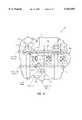
- FIG. 6is a schematic diagram of a section of a DRAM memory system 600 which includes a plurality of multi-port DRAM cell arrays 601, 602 and 603.
- Each of cell arrays 601-603includes an array of dual-port DRAM cells, each of which is identical to the previously described dual-port cell 400.
- DRAM cell array 601includes dual-port memory cells 610a-610n, 611a-611n, 612a-612n and 613a-613n.
- Each of cell arrays 601-603is coupled to two dedicated wordline driver circuits.
- cell array 601is coupled to first port wordline driver circuit 621 and second port wordline driver circuit 622.
- First port wordline driver circuit 621is located to the left of cell array 601, and second port wordline driver circuit 622 is located on the right of cell array 601.
- First port wordline driver circuit 621is coupled to a plurality of first port wordlines 630-633.
- Each of the first port wordlines 630-633is coupled to a first port access transistor (which corresponds to transistor 401 in FIG. 4) in a corresponding row of cells.
- wordline 630is coupled to the first port access transistor in each of memory cells 610a-610n.
- the second port wordline driver circuit 622is coupled to a plurality of second port wordlines 640-643.
- Each of the second port wordlines 640-643is coupled to a second port access transistor (which corresponds to transistor 402 in FIG. 4) in a corresponding row of cells.
- second port wordline 640is coupled to the second port access transistor in each of memory cells 610a-610n.
- a plurality of first port bitlines 660a-660n and second port bitlines 661a-661nare coupled to the columns of DRAM cells. More specifically, a first port bitline is coupled to the first port of each DRAM cell in cell array 601. Similarly, a second port bitline is coupled to the second port of each DRAM cell in cell array 601. For example, first port bitline 660a is coupled to the first port of each of cells 610a-613a, and second port bitline 661a is coupled to the second port of each of cells 610a-613a.
- Each of the first port bitlines 660a-660nis coupled to a corresponding one of sense amplifiers 680a-680n in first port sense amplifier circuit 670.
- first port bitline 660ais coupled to sense amplifier 680a.
- each of the second port bitlines 661a-661nis coupled to a corresponding one of sense amplifier 681a-681n in second port sense amplifier circuit 671.
- second port bitline 661ais coupled to sense amplifier 681a.
- each of the sense amplifiers 680a-680n and 681a-681nis identical to the previously described sense amplifier 500 (FIG. 5).
- DRAM cell arrays 602 and 603are substantially identical to DRAM cell array 601.
- Each of the sense amplifiers 680a-680n in first port sense amplifier circuit 670is coupled to receive a corresponding one of the first port bitlines 690a-690n from cell array 602.
- each of the sense amplifiers 681a-681n in second port sense amplifier circuit 671is coupled to receive a corresponding one of the second port bitlines 691a-691n from cell array 603.
- This architectureis referred to as an open bitline architecture.
- the memory cells in the cell arrays 601-603can be accessed in an overlapping manner (overlapping access).
- the first port wordline driver 621can assert a wordline enable signal on first port wordline 630 to cause data values to be read from the first ports of cells 610a-610n to first port sense amplifier circuit 670 on first port bitlines 660a-660n.
- the second port wordline driver 622can assert a wordline enable signal on second port wordline 640 to cause these data values to be read from the second ports of cells 610a-610n to second part sense amplifier circuit 680 on second port bitlines 661a-661n.
- simultaneous write operationscan be performed at the first port and the second port of the DRAM cells located in the same row of the cell array (i.e., cells 610a-610n).
- simultaneous write operationwould result in an indeterminate data value being written to these DRAM cells.
- the second port wordline driver 622can assert a wordline enable signal on second port wordline 641 to cause data values to be read from the second ports of memory cells 611a-611n to second port sense amplifier circuit 671 on second port bitlines 661a-661n.
- simultaneous read operationscan be performed at different ports of memory cells in different rows of the same cell array.
- the first port wordline driver circuit 621can assert a wordline enable signal on first port wordline 631, and data values can be provided from first port sense amplifier circuit 670 to the first ports of memory cells 611a-611n on first port bitlines 660a-660n, thereby causing data values to be written into memory cells 611a-611n.
- the second port wordline driver circuit 622can assert a wordline enable signal on the second port wordline 640, thereby causing data values to be read from the second ports of cells 610a-610n to second port sense amplifier circuit 671 on second port bitlines 661a-661n.
- the second port wordline driver circuit 622can assert a wordline enable signal on second port wordline 641, thereby causing these data values to be read out of the second ports of memory cells 611a-611n.
- dual-port DRAM cells in accordance with the present inventionfacilitate overlapping accesses. That is, both read and write accesses can be performed at either port of the dual-port DRAM cells of the cell arrays 601-603.
- DRAM cellsare refreshed by performing a read access followed by a write access (i.e., a read/write-back access).
- a read accessfollowed by a write access (i.e., a read/write-back access).
- both the read port and the write portmust be accessed to accomplish a refresh operation.
- refresh operationscan be performed at either port of these dual-port DRAM cells. This provides additional flexibility in operating the memory system 600.
- a conventional DRAM cellhas a slower access speed than a conventional SRAM cell.
- the previously described overlapping access capabilityenables memory system 600 to be operated at an access speed which matches or exceeds the access speed of a conventional SRAM cell array. This capability is illustrated by the following example.
- read accesses 1-4could be carried out as follows. Initially, read access 1 could be initiated at the first port of cells 610a-610n in the manner previously described. At the same time, read access 2 could be initiated at the second port of cells 611a-611n. After read access 1 is completed, read access 3 can be initiated at the first port of cells 612a-612n.
- read access 4can be initiated at the second port of cells 613a-613n. Because read accesses 1 and 2 and read accesses 3 and 4 are performed in parallel, the average access time associated with memory system 600 is approximately twice as fast as a conventional single port DRAM cell. Consecutive write accesses and consecutive read and write accesses can be implemented in a similar manner.
- wordline coupling noiseOne problem facing a designer of memory cell arrays is the wordline coupling noise.
- the voltage on a wordlinedrops from V CC to V SS or jumps from V SS to V CC , the sudden change in voltage in a wordline creates a capacitive effect on the bitlines.
- asserting or de-asserting a logic high wordline enable voltagemay cause a small voltage ripple in the bitlines.
- the noise caused by this capacitive effectis called wordline coupling noise.
- Wordline coupling noisecan become significant in an open bitline architecture, because each sense amplifier is connected to two different arrays that may not be accessed at the same time.
- the cell array 602may not be accessed.
- a voltage ripplemay exist on first port bitlines 660a-660n of cell array 601, while no voltage ripple exists on first port bitlines 690a-690n of cell array 602.
- the voltage ripple existing on first port bitlines 660a-660ncan be effectively canceled by introducing a similar voltage ripple on bitlines 690a-690n.
- a dummy wordline(which is not coupled to any DRAM cells, but passes over the bitlines) is included in cell array 602.
- the dummy wordline in cell array 602is also activated. This creates a voltage ripple on first port bitlines 690a-690n of cell array 602 which is similar to the voltage ripple on the first port bitlines 660a-660n of cell array 601, effectively canceling the noise in the sense amplifiers 680a-680n of first port sense amplifier circuit 670.
- Bitlines 660a-660b and 661a-661b of cell array 601bitlines 690a-690n of cell array 602 and bitlines 691a-691n of cell array 603 have equal length and therefore equal capacitance. This balanced capacitance facilitates the equalization of the bitlines to V CCH .
- each of the end cell arraysis coupled to a sense amplifier circuit which is only coupled to one set of bitlines. To balance the capacitive loading on these edge sense amplifier circuits, these sense amplifier circuits can be coupled to dummy loads and/or dummy arrays to balance the capacitive loading on these sense amplifier circuits.
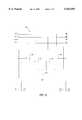
- FIG. 7is a schematic diagram illustrating a dummy array 802 coupled to an edge sense amplifier circuit 833.
- a dummy arraycan be as large as one of the regular cell arrays 601, 602 or 603, in FIG. 7, the dummy array 803 is only half the size of these regular cell arrays.
- the number of rows in dummy array 802is equal to half the number of rows in a regular cell array.
- the bitlines in the dummy array 802are folded such that each bitline is connected to the same number of cells in dummy array 802 as in a regular cell array.
- dummy bitline 820is connected to both the first and second ports of cells 811, 812, and 813, in the first column of dummy array 802.
- Each sense amplifier of edge sense amplifier circuit 833is thus connected to two bitlines with approximately equal capacitance, thereby balancing the capacitive load on edge sense amplifier circuit 833.
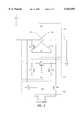
- FIG. 8is a schematic view of the layout of dual-port DRAM cell 400 in accordance with one embodiment of the present invention.
- cell 400is fabricated on a p-type semiconductor region 801 of a semiconductor substrate 800.
- Substrate 800is typically monocrystalline silicon.
- the first port wordline 406 and the second port wordline 405are formed in a polysilicon layer which extends over substrate 800.
- the wordline polysiliconmay be further strapped with a metal layer to reduce its resistance.
- the first port bitline 411 and the second port bitline 412are formed in a separate polysilicon, silicide or metal layer which extends over substrate 800.
- N-type source region 802 and n-type drain regions 803 and 804are formed in p-type semiconductor region 801 as illustrated.
- Source region 802acts as the source for both the first and second port access transistors 401 and 402.
- N-type drain region 803is the drain region for first port access transistor 401
- n-type drain region 804is the drain region for second port access transistor 402.
- Vias 421connect the source region 802 to a capacitor structure in accordance with a conventional capacitor-on-bitline (COB) architecture.
- This capacitor structure(which is not shown in FIG. 8 for purposes of clarity) can include one or more capacitors.
- Drain regions 803 and 804are connected to first port bitline 411 and second port bitline 412, respectively, by conductive vias 822 and 823, respectively.
- the layout of dual-port DRAM cell 400 described abovedoes not require an area consuming gate-to-drain connection.
- the layout area of dual-port DRAM cell 400is smaller than the layout area of either of conventional dual-port DRAM cells 200 or 300 (FIGS. 2 and 3).
- a COB architectureis illustrated in FIG. 8, other capacitor architectures, including, but not limited to trench capacitors, finned capacitors, trench-finned capacitors or stacked capacitors, can be used in DRAM cell 400.
- the drain regions 803 and 804extend beyond DRAM cell 400, thereby providing drain regions in adjacent DRAM cells in the same column as DRAM cell 400. Adjacent cells in the same column are symmetrical about their common boundary. As a result, via 822 provides a bitline contact for the first port access transistor 401 of cell 400, and for the first port access transistor in an adjacent cell (not shown). Similarly, via 823 provides a bitline contact for the second port access transistor 401 of cell 400, and for the second port access transistor in an adjacent cell (not shown). Sharing the bitline contacts among adjacent cells minimizes the number of bitline contacts required per cell, thereby further simplifying and minimizing the required layout area of cell 400.
- FIG. 9is a schematic diagram illustrating a four-port DRAM cell 900 in accordance with one embodiment of the present invention.
- Four-port DRAM cell 900includes a storage capacitor 920 which is connected to first port bitline 911, second port bitline 912, third port bitline 913 and fourth port bitline 914 through first port access transistor 901, second port access transistor 902, third port access transistor 903 and fourth port access transistor 904, respectively.
- First port wordline 905, second port wordline 906, third port wordline 907 and fourth port wordline 908are coupled to the gates of first port access transistor 901, second port access transistor 902, third port access transistor 903 and fourth port access transistor 904, respectively.
- Four-port DRAM cell 900is accessible in a manner similar to dual-port DRAM cell 400, but with two additional available ports. The number of ports can be as numerous as necessary for a particular application.
Landscapes
- Engineering & Computer Science (AREA)
- Microelectronics & Electronic Packaging (AREA)
- Dram (AREA)
Abstract
Description
Claims (15)
Priority Applications (1)
| Application Number | Priority Date | Filing Date | Title |
|---|---|---|---|
| US08/767,707US5923593A (en) | 1996-12-17 | 1996-12-17 | Multi-port DRAM cell and memory system using same |
Applications Claiming Priority (1)
| Application Number | Priority Date | Filing Date | Title |
|---|---|---|---|
| US08/767,707US5923593A (en) | 1996-12-17 | 1996-12-17 | Multi-port DRAM cell and memory system using same |
Publications (1)
| Publication Number | Publication Date |
|---|---|
| US5923593Atrue US5923593A (en) | 1999-07-13 |
Family
ID=25080304
Family Applications (1)
| Application Number | Title | Priority Date | Filing Date |
|---|---|---|---|
| US08/767,707Expired - LifetimeUS5923593A (en) | 1996-12-17 | 1996-12-17 | Multi-port DRAM cell and memory system using same |
Country Status (1)
| Country | Link |
|---|---|
| US (1) | US5923593A (en) |
Cited By (49)
| Publication number | Priority date | Publication date | Assignee | Title |
|---|---|---|---|---|
| WO2000019437A3 (en)* | 1998-09-30 | 2000-05-25 | Siemens Ag | Dual-port memory location |
| US6137713A (en)* | 1998-10-20 | 2000-10-24 | Matsushita Electric Industrial Co., Ltd. | Semiconductor storage device |
| US6170046B1 (en) | 1997-10-28 | 2001-01-02 | Mmc Networks, Inc. | Accessing a memory system via a data or address bus that provides access to more than one part |
| US6169684B1 (en) | 1999-02-02 | 2001-01-02 | Matsushita Electric Industrial Co., Ltd. | Semiconductor memory device |
| US6181620B1 (en) | 1999-01-29 | 2001-01-30 | Matsushita Electric Industrial Co., Ltd. | Semiconductor storage device |
| US6222786B1 (en) | 1999-11-02 | 2001-04-24 | Silicon Aquarius, Inc. | Dynamic random access memory with write-without-restore and systems and methods using the same |
| US6226223B1 (en) | 1999-02-24 | 2001-05-01 | Matsushita Electric Industrial Co., Ltd. | Low latency dynamic random access memory |
| US20010034817A1 (en)* | 2000-04-20 | 2001-10-25 | International Business Machines Corporation | Read/write alignment scheme for port red uction of multi-port SRAM cells |
| US6317358B1 (en) | 2000-08-03 | 2001-11-13 | Micron Technology, Inc. | Efficient dual port DRAM cell using SOI technology |
| US6400629B1 (en) | 2001-06-29 | 2002-06-04 | International Business Machines Corporation | System and method for early write to memory by holding bitline at fixed potential |
| US6438016B1 (en) | 2000-08-30 | 2002-08-20 | Micron Technology, Inc. | Semiconductor memory having dual port cell supporting hidden refresh |
| US6445638B1 (en) | 2000-08-29 | 2002-09-03 | International Business Machines Corporation | Folded-bitline dual-port DRAM architecture system |
| US6477079B2 (en)* | 1999-05-18 | 2002-11-05 | Kabushiki Kaisha Toshiba | Voltage generator for semiconductor device |
| EP1258888A2 (en)* | 2001-05-14 | 2002-11-20 | Infineon Technologies AG | Multi-port memory cell with refresh port |
| US6504766B1 (en) | 2001-06-29 | 2003-01-07 | International Business Machines Corporation | System and method for early write to memory by injecting small voltage signal |
| US20030008416A1 (en)* | 2001-04-16 | 2003-01-09 | Nec Corporation | Magnetoresistive device and method of producing the same |
| US20030043653A1 (en)* | 2001-09-06 | 2003-03-06 | Matsushita Electric Industrial Co., Ltd. | Semiconductor memory device |
| US20030117832A1 (en)* | 2001-12-21 | 2003-06-26 | Mitsubishi Denki Kabushiki Kaisha | Semiconductor memory device having two-transistor, one-capacitor type memory cells of high data holding characteristic |
| US20030151943A1 (en)* | 2002-02-14 | 2003-08-14 | Matsushita Electric Industrial Co., Ltd. | Semiconductor memory |
| US20040037107A1 (en)* | 2002-08-26 | 2004-02-26 | Mitsubishi Denki Kabushiki Kaisha | Semiconductor storage device including random access memory cells having a plurality of indendently accessible access ports |
| US20040057315A1 (en)* | 2002-09-25 | 2004-03-25 | Jain Raj Kumar | Refresh control circuit for ICs with a memory array |
| WO2004027781A1 (en)* | 2002-09-19 | 2004-04-01 | Infineon Technologies Ag | Refreshing of multi-port memory in integrated circuits |
| US6724645B1 (en)* | 2003-01-30 | 2004-04-20 | Agilent Technologies, Inc. | Method and apparatus for shortening read operations in destructive read memories |
| US6778466B2 (en) | 2002-04-11 | 2004-08-17 | Fujitsu Limited | Multi-port memory cell |
| US6853578B1 (en)* | 2002-03-18 | 2005-02-08 | Piconetics, Inc. | Pulse driven single bit line SRAM cell |
| US20050047238A1 (en)* | 2003-09-03 | 2005-03-03 | Ruggero Castagnetti | Reconfigurable memory arrays |
| US20050047254A1 (en)* | 2003-08-27 | 2005-03-03 | Ramnath Venkatraman | Design and use of a spacer cell to support reconfigurable memories |
| US20050146921A1 (en)* | 2003-12-30 | 2005-07-07 | Yibin Ye | 1P1N 2T gain cell |
| US20050226079A1 (en)* | 2004-04-08 | 2005-10-13 | Yiming Zhu | Methods and apparatus for dual port memory devices having hidden refresh and double bandwidth |
| US20050273544A1 (en)* | 2003-07-31 | 2005-12-08 | Fitzsimmons Michael D | Method of accessing memory via multiple slave ports |
| US20050289293A1 (en)* | 2004-06-28 | 2005-12-29 | Parris Michael C | Dual-port DRAM cell with simultaneous access |
| WO2005089086A3 (en)* | 2003-08-26 | 2006-02-09 | Ibm | Method and apparatus for read bitline clamping for gain cell dram devices |
| US7145829B1 (en) | 2005-06-16 | 2006-12-05 | International Business Machines Corporation | Single cycle refresh of multi-port dynamic random access memory (DRAM) |
| US20070002617A1 (en)* | 2005-06-30 | 2007-01-04 | Texas Instruments Incorporated | Area efficient implementation of small blocks in an SRAM array |
| US20070127305A1 (en)* | 2005-11-24 | 2007-06-07 | Kabushiki Kaisha Toshiba | Semiconductor memory |
| US20070150668A1 (en)* | 2005-12-22 | 2007-06-28 | Samsung Electronics Co., Ltd. | Multi-path accessible semiconductor memory device |
| US20070268742A1 (en)* | 2006-05-18 | 2007-11-22 | Micron Technology, Inc. | Memory Architecture and Cell Design Employing Two Access Transistors |
| US20080005492A1 (en)* | 2006-06-29 | 2008-01-03 | Monolithic System Technology, Inc. | Dual-Port SRAM Memory Using Single-Port Memory Cell |
| US20080002453A1 (en)* | 2006-06-28 | 2008-01-03 | Taiwan Semiconductor Manufacturing Company, Ltd. | Multiple port resistive memory cell |
| CN100476785C (en)* | 2001-02-24 | 2009-04-08 | 国际商业机器公司 | Device and method for computing structures |
| US20090097301A1 (en)* | 2005-06-01 | 2009-04-16 | Matsushita Electric Industrial Co., Ltd. | Semiconductor storage apparatus and semiconductor integrated circuit incorporating the same |
| US20100090286A1 (en)* | 2008-10-09 | 2010-04-15 | Seung-Jun Lee | Vertical-type semiconductor device and method of manufacturing the same |
| US20100110773A1 (en)* | 2008-07-07 | 2010-05-06 | Manoj Sachdev | Sram cell without dedicated access transistors |
| US20110228594A1 (en)* | 2010-03-22 | 2011-09-22 | Qualcomm Incorporated | Multi-Port Non-Volatile Memory that Includes a Resistive Memory Element |
| US8171234B2 (en) | 2009-03-16 | 2012-05-01 | Mosys, Inc. | Multi-bank multi-port architecture |
| US8760912B2 (en) | 2008-12-04 | 2014-06-24 | Tiraboschi Services, Llc | Eight transistor soft error robust storage cell |
| US9666254B1 (en)* | 2015-11-06 | 2017-05-30 | SK Hynix Inc. | Semiconductor memory apparatus having open bit line structure in which a sense amplifier array shared between a dummy array and normal array,comparing one bit line of the normal array with two or more bit lines of the dummy array |
| US20170236587A1 (en)* | 2016-02-16 | 2017-08-17 | Renesas Electronics Corporation | Flash memory |
| US10409742B2 (en) | 2015-10-07 | 2019-09-10 | Rambus Inc. | Interface for memory readout from a memory component in the event of fault |
Citations (4)
| Publication number | Priority date | Publication date | Assignee | Title |
|---|---|---|---|---|
| US5007022A (en)* | 1987-12-21 | 1991-04-09 | Texas Instruments Incorporated | Two-port two-transistor DRAM |
| US5355335A (en)* | 1991-06-25 | 1994-10-11 | Fujitsu Limited | Semiconductor memory device having a plurality of writing and reading ports for decreasing hardware amount |
| US5646903A (en)* | 1996-03-06 | 1997-07-08 | Xilinx, Inc. | Memory cell having a shared read/write line |
| US5768178A (en)* | 1995-06-30 | 1998-06-16 | Micron Technology, Inc. | Data transfer circuit in a memory device |
- 1996
- 1996-12-17USUS08/767,707patent/US5923593A/ennot_activeExpired - Lifetime
Patent Citations (4)
| Publication number | Priority date | Publication date | Assignee | Title |
|---|---|---|---|---|
| US5007022A (en)* | 1987-12-21 | 1991-04-09 | Texas Instruments Incorporated | Two-port two-transistor DRAM |
| US5355335A (en)* | 1991-06-25 | 1994-10-11 | Fujitsu Limited | Semiconductor memory device having a plurality of writing and reading ports for decreasing hardware amount |
| US5768178A (en)* | 1995-06-30 | 1998-06-16 | Micron Technology, Inc. | Data transfer circuit in a memory device |
| US5646903A (en)* | 1996-03-06 | 1997-07-08 | Xilinx, Inc. | Memory cell having a shared read/write line |
Cited By (89)
| Publication number | Priority date | Publication date | Assignee | Title |
|---|---|---|---|---|
| US6170046B1 (en) | 1997-10-28 | 2001-01-02 | Mmc Networks, Inc. | Accessing a memory system via a data or address bus that provides access to more than one part |
| WO2000019437A3 (en)* | 1998-09-30 | 2000-05-25 | Siemens Ag | Dual-port memory location |
| US6552951B1 (en) | 1998-09-30 | 2003-04-22 | Infineon Technologies Ag | Dual-port memory location |
| US6137713A (en)* | 1998-10-20 | 2000-10-24 | Matsushita Electric Industrial Co., Ltd. | Semiconductor storage device |
| US6181620B1 (en) | 1999-01-29 | 2001-01-30 | Matsushita Electric Industrial Co., Ltd. | Semiconductor storage device |
| US6169684B1 (en) | 1999-02-02 | 2001-01-02 | Matsushita Electric Industrial Co., Ltd. | Semiconductor memory device |
| US6226223B1 (en) | 1999-02-24 | 2001-05-01 | Matsushita Electric Industrial Co., Ltd. | Low latency dynamic random access memory |
| US6477079B2 (en)* | 1999-05-18 | 2002-11-05 | Kabushiki Kaisha Toshiba | Voltage generator for semiconductor device |
| US6532167B2 (en) | 1999-05-18 | 2003-03-11 | Kabushiki Kaisha Toshiba | Voltage generator for semiconductor device |
| US6222786B1 (en) | 1999-11-02 | 2001-04-24 | Silicon Aquarius, Inc. | Dynamic random access memory with write-without-restore and systems and methods using the same |
| US6785781B2 (en)* | 2000-04-20 | 2004-08-31 | International Business Machines Corporation | Read/write alignment scheme for port reduction of multi-port SRAM cells |
| US20010034817A1 (en)* | 2000-04-20 | 2001-10-25 | International Business Machines Corporation | Read/write alignment scheme for port red uction of multi-port SRAM cells |
| US6317358B1 (en) | 2000-08-03 | 2001-11-13 | Micron Technology, Inc. | Efficient dual port DRAM cell using SOI technology |
| US6445638B1 (en) | 2000-08-29 | 2002-09-03 | International Business Machines Corporation | Folded-bitline dual-port DRAM architecture system |
| US6504204B1 (en) | 2000-08-29 | 2003-01-07 | Ibm Corporation | Compact dual-port DRAM architecture system and method for making same |
| US6545935B1 (en) | 2000-08-29 | 2003-04-08 | Ibm Corporation | Dual-port DRAM architecture system |
| US6438016B1 (en) | 2000-08-30 | 2002-08-20 | Micron Technology, Inc. | Semiconductor memory having dual port cell supporting hidden refresh |
| WO2002019341A3 (en)* | 2000-08-30 | 2003-04-03 | Micron Technology Inc | Semiconductor memory having dual port cell supporting hidden refresh |
| EP2287849A3 (en)* | 2000-08-30 | 2011-03-09 | Micron Technology, Inc. | Semiconductor memory having dual port cell supporting hidden refresh |
| US6757200B2 (en) | 2000-08-30 | 2004-06-29 | Micron Technology, Inc. | Semiconductor memory having dual port cell supporting hidden refresh |
| CN100476785C (en)* | 2001-02-24 | 2009-04-08 | 国际商业机器公司 | Device and method for computing structures |
| US20030008416A1 (en)* | 2001-04-16 | 2003-01-09 | Nec Corporation | Magnetoresistive device and method of producing the same |
| EP1258888A2 (en)* | 2001-05-14 | 2002-11-20 | Infineon Technologies AG | Multi-port memory cell with refresh port |
| US6504766B1 (en) | 2001-06-29 | 2003-01-07 | International Business Machines Corporation | System and method for early write to memory by injecting small voltage signal |
| US6400629B1 (en) | 2001-06-29 | 2002-06-04 | International Business Machines Corporation | System and method for early write to memory by holding bitline at fixed potential |
| US6751116B2 (en) | 2001-09-06 | 2004-06-15 | Matsushita Electric Industrial Co., Ltd. | Semiconductor memory device |
| US7031199B2 (en) | 2001-09-06 | 2006-04-18 | Matsushita Electric Industrial Co., Ltd. | Semiconductor memory device |
| US20030043653A1 (en)* | 2001-09-06 | 2003-03-06 | Matsushita Electric Industrial Co., Ltd. | Semiconductor memory device |
| US20040184322A1 (en)* | 2001-09-06 | 2004-09-23 | Matsushita Electric Industrial Co., Ltd | Semiconductor memory device |
| US6859384B2 (en) | 2001-12-21 | 2005-02-22 | Renesas Technology Corp. | Semiconductor memory device having two-transistor, one-capacitor type memory cells of high data holding characteristic |
| US20030117832A1 (en)* | 2001-12-21 | 2003-06-26 | Mitsubishi Denki Kabushiki Kaisha | Semiconductor memory device having two-transistor, one-capacitor type memory cells of high data holding characteristic |
| US6711050B2 (en) | 2002-02-14 | 2004-03-23 | Matsushita Electric Industrial Co., Ltd. | Semiconductor memory |
| US20030151943A1 (en)* | 2002-02-14 | 2003-08-14 | Matsushita Electric Industrial Co., Ltd. | Semiconductor memory |
| US6853578B1 (en)* | 2002-03-18 | 2005-02-08 | Piconetics, Inc. | Pulse driven single bit line SRAM cell |
| US6778466B2 (en) | 2002-04-11 | 2004-08-17 | Fujitsu Limited | Multi-port memory cell |
| US20040037107A1 (en)* | 2002-08-26 | 2004-02-26 | Mitsubishi Denki Kabushiki Kaisha | Semiconductor storage device including random access memory cells having a plurality of indendently accessible access ports |
| WO2004027781A1 (en)* | 2002-09-19 | 2004-04-01 | Infineon Technologies Ag | Refreshing of multi-port memory in integrated circuits |
| US20040057315A1 (en)* | 2002-09-25 | 2004-03-25 | Jain Raj Kumar | Refresh control circuit for ICs with a memory array |
| US7002867B2 (en)* | 2002-09-25 | 2006-02-21 | Infineon Technologies Aktiengesellschaft | Refresh control circuit for ICs with a memory array |
| US6724645B1 (en)* | 2003-01-30 | 2004-04-20 | Agilent Technologies, Inc. | Method and apparatus for shortening read operations in destructive read memories |
| US7185121B2 (en)* | 2003-07-31 | 2007-02-27 | Freescale Semiconductor, Inc. | Method of accessing memory via multiple slave ports |
| US20050273544A1 (en)* | 2003-07-31 | 2005-12-08 | Fitzsimmons Michael D | Method of accessing memory via multiple slave ports |
| WO2005089086A3 (en)* | 2003-08-26 | 2006-02-09 | Ibm | Method and apparatus for read bitline clamping for gain cell dram devices |
| CN100429702C (en)* | 2003-08-26 | 2008-10-29 | 国际商业机器公司 | Method and apparatus for read bitline clamping for gain cell DRAM devices |
| KR100791367B1 (en) | 2003-08-26 | 2008-01-07 | 인터내셔널 비지네스 머신즈 코포레이션 | Method and device for read bitline clamping in a gain cell DRAM device |
| US20050047254A1 (en)* | 2003-08-27 | 2005-03-03 | Ramnath Venkatraman | Design and use of a spacer cell to support reconfigurable memories |
| US7006369B2 (en)* | 2003-08-27 | 2006-02-28 | Lsi Logic Corporation | Design and use of a spacer cell to support reconfigurable memories |
| US20050047238A1 (en)* | 2003-09-03 | 2005-03-03 | Ruggero Castagnetti | Reconfigurable memory arrays |
| US6934174B2 (en) | 2003-09-03 | 2005-08-23 | Lsi Logic Corporation | Reconfigurable memory arrays |
| US7123500B2 (en)* | 2003-12-30 | 2006-10-17 | Intel Corporation | 1P1N 2T gain cell |
| US20050146921A1 (en)* | 2003-12-30 | 2005-07-07 | Yibin Ye | 1P1N 2T gain cell |
| US20050226079A1 (en)* | 2004-04-08 | 2005-10-13 | Yiming Zhu | Methods and apparatus for dual port memory devices having hidden refresh and double bandwidth |
| US20050289293A1 (en)* | 2004-06-28 | 2005-12-29 | Parris Michael C | Dual-port DRAM cell with simultaneous access |
| US20090097301A1 (en)* | 2005-06-01 | 2009-04-16 | Matsushita Electric Industrial Co., Ltd. | Semiconductor storage apparatus and semiconductor integrated circuit incorporating the same |
| US20060285411A1 (en)* | 2005-06-16 | 2006-12-21 | International Business Machines Corporation | Single cycle refresh of multi-port dynamic random access memory (dram) |
| US7145829B1 (en) | 2005-06-16 | 2006-12-05 | International Business Machines Corporation | Single cycle refresh of multi-port dynamic random access memory (DRAM) |
| US20070002617A1 (en)* | 2005-06-30 | 2007-01-04 | Texas Instruments Incorporated | Area efficient implementation of small blocks in an SRAM array |
| US7236396B2 (en)* | 2005-06-30 | 2007-06-26 | Texas Instruments Incorporated | Area efficient implementation of small blocks in an SRAM array |
| US20070127305A1 (en)* | 2005-11-24 | 2007-06-07 | Kabushiki Kaisha Toshiba | Semiconductor memory |
| US7423926B2 (en)* | 2005-11-24 | 2008-09-09 | Kabushiki Kaisha Toshiba | Semiconductor memory |
| US20070150668A1 (en)* | 2005-12-22 | 2007-06-28 | Samsung Electronics Co., Ltd. | Multi-path accessible semiconductor memory device |
| US7606055B2 (en)* | 2006-05-18 | 2009-10-20 | Micron Technology, Inc. | Memory architecture and cell design employing two access transistors |
| US9875795B2 (en) | 2006-05-18 | 2018-01-23 | Micron Technology, Inc. | Memory architecture and cell design employing two access transistors |
| US8730718B2 (en) | 2006-05-18 | 2014-05-20 | Micron Technology, Inc. | Memory architecture and cell design employing two access transistors |
| US8233316B2 (en) | 2006-05-18 | 2012-07-31 | Micron Technology, Inc. | Memory architecture and cell design employing two access transistors |
| US20070268742A1 (en)* | 2006-05-18 | 2007-11-22 | Micron Technology, Inc. | Memory Architecture and Cell Design Employing Two Access Transistors |
| US20100008163A1 (en)* | 2006-05-18 | 2010-01-14 | Micron Technology, Inc. | Memory architecture and cell design employing two access transistors |
| US7403413B2 (en) | 2006-06-28 | 2008-07-22 | Taiwan Semiconductor Manufacturing Company, Ltd. | Multiple port resistive memory cell |
| US20080002453A1 (en)* | 2006-06-28 | 2008-01-03 | Taiwan Semiconductor Manufacturing Company, Ltd. | Multiple port resistive memory cell |
| US20080005492A1 (en)* | 2006-06-29 | 2008-01-03 | Monolithic System Technology, Inc. | Dual-Port SRAM Memory Using Single-Port Memory Cell |
| US7533222B2 (en) | 2006-06-29 | 2009-05-12 | Mosys, Inc. | Dual-port SRAM memory using single-port memory cell |
| US20100110773A1 (en)* | 2008-07-07 | 2010-05-06 | Manoj Sachdev | Sram cell without dedicated access transistors |
| US8072797B2 (en)* | 2008-07-07 | 2011-12-06 | Certichip Inc. | SRAM cell without dedicated access transistors |
| US20100090286A1 (en)* | 2008-10-09 | 2010-04-15 | Seung-Jun Lee | Vertical-type semiconductor device and method of manufacturing the same |
| US8476713B2 (en)* | 2008-10-09 | 2013-07-02 | Samsung Electronics Co., Ltd. | Vertical-type semiconductor device and method of manufacturing the same |
| US9401199B2 (en) | 2008-12-04 | 2016-07-26 | Tiraboschi Services, Llc | Eight transistor soft error robust storage cell |
| US8760912B2 (en) | 2008-12-04 | 2014-06-24 | Tiraboschi Services, Llc | Eight transistor soft error robust storage cell |
| US8171234B2 (en) | 2009-03-16 | 2012-05-01 | Mosys, Inc. | Multi-bank multi-port architecture |
| US8400822B2 (en)* | 2010-03-22 | 2013-03-19 | Qualcomm Incorporated | Multi-port non-volatile memory that includes a resistive memory element |
| US9135974B2 (en) | 2010-03-22 | 2015-09-15 | Qualcomm Incorporated | Multi-port non-volatile memory that includes a resistive memory element |
| US20110228594A1 (en)* | 2010-03-22 | 2011-09-22 | Qualcomm Incorporated | Multi-Port Non-Volatile Memory that Includes a Resistive Memory Element |
| US10409742B2 (en) | 2015-10-07 | 2019-09-10 | Rambus Inc. | Interface for memory readout from a memory component in the event of fault |
| US11308009B2 (en) | 2015-10-07 | 2022-04-19 | Rambus Inc. | Interface for memory readout from a memory component in the event of fault |
| US11625346B2 (en) | 2015-10-07 | 2023-04-11 | Rambus Inc. | Interface for memory readout from a memory component in the event of fault |
| US12066957B2 (en) | 2015-10-07 | 2024-08-20 | Rambus Inc. | Interface for memory readout from a memory component in the event of fault |
| US9666254B1 (en)* | 2015-11-06 | 2017-05-30 | SK Hynix Inc. | Semiconductor memory apparatus having open bit line structure in which a sense amplifier array shared between a dummy array and normal array,comparing one bit line of the normal array with two or more bit lines of the dummy array |
| US20170236587A1 (en)* | 2016-02-16 | 2017-08-17 | Renesas Electronics Corporation | Flash memory |
| US9947409B2 (en)* | 2016-02-16 | 2018-04-17 | Renesas Electronics Corporation | Flash memory |
| US10192621B2 (en) | 2016-02-16 | 2019-01-29 | Renesas Electronics Corporation | Flash memory |
Similar Documents
| Publication | Publication Date | Title |
|---|---|---|
| US5923593A (en) | Multi-port DRAM cell and memory system using same | |
| US4584672A (en) | CMOS dynamic random-access memory with active cycle one half power supply potential bit line precharge | |
| KR100646972B1 (en) | 3T1D Memory Cells Using Gated Diodes and Methods of Use Thereof | |
| US6982897B2 (en) | Nondestructive read, two-switch, single-charge-storage device RAM devices | |
| JP3874234B2 (en) | Semiconductor integrated circuit device | |
| KR100650244B1 (en) | Gated diode memory cells | |
| US5315555A (en) | Sense amplifier for performing a high-speed sensing operation | |
| US7613057B2 (en) | Circuit and method for a sense amplifier | |
| EP1120791A1 (en) | Semiconductor device | |
| US7800965B2 (en) | Digit line equilibration using access devices at the edge of sub-arrays | |
| US20050281110A1 (en) | Semiconductor integrated circuit device | |
| US20060198210A1 (en) | Semiconductor device | |
| US6898137B2 (en) | Semiconductor memory device with high-speed sense amplifier | |
| US20230005522A1 (en) | Readout circuit structure | |
| JPH0836885A (en) | Dynamic random-access memory | |
| US6049492A (en) | Interleaved sense amplifier with a single-sided precharge device | |
| US5666306A (en) | Multiplication of storage capacitance in memory cells by using the Miller effect | |
| US6768143B1 (en) | Structure and method of making three finger folded field effect transistors having shared junctions | |
| US6928012B2 (en) | Bitline equalization system for a DRAM integrated circuit | |
| WO1985002314A2 (en) | Semiconductor memory | |
| JPS6255234B2 (en) | ||
| US20250118360A1 (en) | Memory device, assist cell and double assist cell for a memory device | |
| US20250259669A1 (en) | Embedded dynamic memory, implementation method of embedded dynamic memory, and integrated circuit | |
| US6621752B2 (en) | Refreshing scheme for memory cells a memory array to increase performance of integrated circuits | |
| US20250118362A1 (en) | Banked sense amplifier circuit for a memory core and a memory core complex |
Legal Events
| Date | Code | Title | Description |
|---|---|---|---|
| AS | Assignment | Owner name:MONOLITHIC SYSTEMS, INC., CALIFORNIA Free format text:ASSIGNMENT OF ASSIGNORS INTEREST;ASSIGNORS:HSU, FU-CHIEH;LEUNG, WINGYU;REEL/FRAME:008479/0199 Effective date:19970425 | |
| STCF | Information on status: patent grant | Free format text:PATENTED CASE | |
| AS | Assignment | Owner name:MONOLITHIC SYSTEM TECHNOLOGY, INC., CALIFORNIA Free format text:ASSIGNMENT OF ASSIGNORS INTEREST;ASSIGNORS:HSU, FU-CHIEH;LEUNG, WINGYU;REEL/FRAME:010321/0469 Effective date:19991012 | |
| FEPP | Fee payment procedure | Free format text:PAT HOLDER NO LONGER CLAIMS SMALL ENTITY STATUS, ENTITY STATUS SET TO UNDISCOUNTED (ORIGINAL EVENT CODE: STOL); ENTITY STATUS OF PATENT OWNER: LARGE ENTITY Free format text:PAYOR NUMBER ASSIGNED (ORIGINAL EVENT CODE: ASPN); ENTITY STATUS OF PATENT OWNER: LARGE ENTITY | |
| REFU | Refund | Free format text:REFUND - SURCHARGE, PETITION TO ACCEPT PYMT AFTER EXP, UNINTENTIONAL (ORIGINAL EVENT CODE: R2551); ENTITY STATUS OF PATENT OWNER: LARGE ENTITY | |
| FPAY | Fee payment | Year of fee payment:4 | |
| FPAY | Fee payment | Year of fee payment:8 | |
| AS | Assignment | Owner name:MOSYS, INC., CALIFORNIA Free format text:CHANGE OF NAME;ASSIGNOR:MONOLITHIC SYSTEM TECHNOLOGY, INC.;REEL/FRAME:020741/0975 Effective date:20060525 Owner name:MOSYS, INC.,CALIFORNIA Free format text:CHANGE OF NAME;ASSIGNOR:MONOLITHIC SYSTEM TECHNOLOGY, INC.;REEL/FRAME:020741/0975 Effective date:20060525 | |
| FPAY | Fee payment | Year of fee payment:12 | |
| AS | Assignment | Owner name:INGALLS & SNYDER LLC, NEW YORK Free format text:SECURITY INTEREST;ASSIGNOR:MOSYS, INC.;REEL/FRAME:038081/0262 Effective date:20160314 | |
| AS | Assignment | Owner name:INGALLS & SNYDER LLC, NEW YORK Free format text:RELEASE BY SECURED PARTY;ASSIGNOR:PERASO INC. F/K/A MOSYS, INC.;REEL/FRAME:061593/0094 Effective date:20221003 |