US5923180A - Compliant wafer prober docking adapter - Google Patents
Compliant wafer prober docking adapterDownload PDFInfo
- Publication number
- US5923180A US5923180AUS08/794,821US79482197AUS5923180AUS 5923180 AUS5923180 AUS 5923180AUS 79482197 AUS79482197 AUS 79482197AUS 5923180 AUS5923180 AUS 5923180A
- Authority
- US
- United States
- Prior art keywords
- docking
- adapter
- test head
- fixture board
- wafer
- Prior art date
- Legal status (The legal status is an assumption and is not a legal conclusion. Google has not performed a legal analysis and makes no representation as to the accuracy of the status listed.)
- Expired - Fee Related
Links
- 238000003032molecular dockingMethods0.000titleclaimsabstractdescription112
- 238000012360testing methodMethods0.000claimsabstractdescription118
- 230000007246mechanismEffects0.000claimsabstractdescription13
- 239000000523sampleSubstances0.000claimsdescription21
- 241000239290AraneaeSpecies0.000claimsdescription20
- 238000000034methodMethods0.000abstractdescription16
- 230000008569processEffects0.000abstractdescription16
- 230000013011matingEffects0.000abstractdescription7
- 239000000463materialSubstances0.000description7
- 238000012986modificationMethods0.000description5
- 230000004048modificationEffects0.000description5
- 238000013459approachMethods0.000description4
- 230000003044adaptive effectEffects0.000description2
- 229920004943Delrin®Polymers0.000description1
- 241000755266Kathetostoma giganteumSpecies0.000description1
- 230000006978adaptationEffects0.000description1
- XAGFODPZIPBFFR-UHFFFAOYSA-NaluminiumChemical compound[Al]XAGFODPZIPBFFR-UHFFFAOYSA-N0.000description1
- 229910052782aluminiumInorganic materials0.000description1
- 230000003321amplificationEffects0.000description1
- 239000003990capacitorSubstances0.000description1
- 230000006835compressionEffects0.000description1
- 238000007906compressionMethods0.000description1
- 230000003750conditioning effectEffects0.000description1
- 238000011156evaluationMethods0.000description1
- 238000001914filtrationMethods0.000description1
- 238000009434installationMethods0.000description1
- 238000005259measurementMethods0.000description1
- 238000003199nucleic acid amplification methodMethods0.000description1
- 230000002093peripheral effectEffects0.000description1
- 238000012545processingMethods0.000description1
- 230000004044responseEffects0.000description1
- 238000000926separation methodMethods0.000description1
- 238000001228spectrumMethods0.000description1
- 239000000758substrateSubstances0.000description1
- 238000013519translationMethods0.000description1
Images


Classifications
- G—PHYSICS
- G01—MEASURING; TESTING
- G01R—MEASURING ELECTRIC VARIABLES; MEASURING MAGNETIC VARIABLES
- G01R31/00—Arrangements for testing electric properties; Arrangements for locating electric faults; Arrangements for electrical testing characterised by what is being tested not provided for elsewhere
- G01R31/28—Testing of electronic circuits, e.g. by signal tracer
- G01R31/2851—Testing of integrated circuits [IC]
- G01R31/2886—Features relating to contacting the IC under test, e.g. probe heads; chucks
- G01R31/2887—Features relating to contacting the IC under test, e.g. probe heads; chucks involving moving the probe head or the IC under test; docking stations
Definitions
- the present inventionrelates to a compliant wafer prober docking adapter for use in a docking system for accurately aligning an electronic test head to a wafer prober.
- a compliant wafer prober docking adapterfor use in a docking system for accurately aligning an electronic test head to a wafer prober.
- Such docking systemsare described, for example, in the above identified U.S. Pat. No. 5,552,701, the details of which are hereby incorporated by reference.
- an adapterin order to speed up the mating of the test system to the wafer prober, an adapter is rigidly affixed to the test head itself such that the test head is moved down upon the wafer.
- the probe tipsare aligned to the wafer by moving the test head (a large mass) around while looking through a periscope through the middle of the test head.
- the compliant wafer prober docking adapterprovides a compliant docking capability.
- the compliant adapterincludes a compliant spring mechanism in the form of coiled springs which support a portion of the weight of a test head wherein the upper portion of the adapter automatically aligns itself with the test head. This desirable aspect allows for all of the connectors to be seated properly, such that the locking engagement provides a compliant and secure mating between the two surfaces, even though the surfaces of the wafer prober and the test head are not perfectly planar.
- Another feature of the present inventionis in connection with the docking process.
- an adapteris rigidly affixed to the test head such that the test head is moved down upon the wafer and the probe tips are aligned to the wafer by moving the test head (a large mass) around while looking through a periscope through the middle of the test head. Using this process, it frequently takes two persons working together to coordinate on properly aligning the two large masses.
- the present inventionprovides for affixing the compliant adapter with an rotational (“theta") adjustment capability which allows for angular alignment of prober tips to a wafer prober (in one embodiment, an angular adjustment within approximately 15 degrees).
- the present inventionallows for one user who can view the alignment process through a television monitor (or microscope) or directly without the complexity and awkwardness of prior art approaches. The head can then be lowered and locked in position and the system is ready to be tested.
- a test headcan be easily moved from one wafer prober to another, because the alignment of the adapter to the wafer prober is not being disturbed. Hence, the test head can be moved back and forth between stations very quickly without having to go through another long and complex re-alignment process.
- FIG. 1is an isometric view of a conventional electronic circuit tester
- FIG. 1ais an isometric view of a device-under-test (DUT) board, which forms a portion of the tester of FIG. 1;
- DUTdevice-under-test
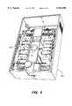
- FIG. 2is an exploded view of a test head, load board, and fixture board of an electronic circuit test system, which incorporate a docking system;
- FIG. 3is a detail of a docking cone and spider comprising the docking system shown in FIG. 2;
- FIG. 4is an exploded detail of the load board, a cam locking ring, and a connector support disk incorporated into the test head of the electronic circuit test system shown in FIG. 2;
- FIG. 5is an isometric view of the obverse of the test head shown in FIG. 2;
- FIG. 6illustrates deployment of the docking system to tester for packaged devices or integrated circuits fed by an automated material handler
- FIG. 7illustrates deployment of a docking system at a wafer probing station to test devices or integrated circuits on wafer.
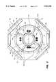
- FIG. 8shows an exploded, isometric view of the compliant wafer prober docking adapter according to the present invention
- FIG. 9shows an exploded, isometric view of a conical spring pair, which forms part of the compliant adapter of FIG. 8;
- FIG. 10shows a cross sectional view of the compliant adapter of FIG. 8
- FIG. 11shows another isometric view of the compliant wafer prober docking adapter attached to the top surface of a wafer prober according to the present invention.
- FIG. 12shows bottom isometric view of the compliant wafer prober docking adapter according to the present invention.
- the electronic circuit tester 10includes a test head 12 electrically connected by cables routed through a conduit 14 to a rack(s) 16 of electronic test and measurement instruments, such as ac and dc electrical signal generators for applying electrical signals to a device or integrated circuit interfaced to the test head, and signal analyzers, for example, a network analyzer, spectrum analyzer, oscilloscope, or other waveform digitizing and/or signal processing equipment, for measuring the response(s) to those applied electrical signals.
- the test head 12can include circuitry which performs distribution of electrical signals, signal separation, frequency translation, amplification, attenuation, switching, or other conditioning or modification of electrical signals prior to being routed to the rack 16 or to a device or integrated circuit being tested.
- the test head 12interfaces to a device or integrated circuit through a load board 18 and in turn through a fixture board 20 typically mounted to the test head.
- a calibration board(not shown) having a configuration similar to the fixture board can be connected to the test head 12 for calibrating the test head.
- the configuration of the load board 18depends on the type or family of device or integrated circuit being tested, such as an analog or digital electronic circuit, while the configuration of the fixture board 20 is typically specific to the family or particular device or integrated circuit being tested.
- the fixture board 20is in turn interfaces to a device-under-test (DUT) board 22 that comprises inductors, capacitors, and/or other electronic components or circuits mounted to or fabricated on the components or circuits mounted to or fabricated on the DUT board for decoupling, filtering, attenuating, or otherwise modifying electrical signals transmitted to and/or received from a device or integrated circuit being tested.
- DUT board 22is connected to a socket 24 for effecting an electrical connection(s) between the electronic circuit tester 10 and the actual electronic circuit being tested, such as a packaged device or integrated circuit 26.
- the test head 12is mounted to a dolly 28.
- the test head 12is mounted by pivotable connections 30 to dolly 28.
- the pivotable connections 30enable the test head 12 to be positioned in an approximately upward facing horizontal position so that the appropriate load board 18 and calibration or fixture board 20 and DUT board with the socket 24 can be mounted to the test head of the electronic circuit tester 10 by an operator.
- the test head 12can also be pivoted to any angular position so that the socket 24 can interface with an automated material handler 32, for example, which rapidly feeds each packaged device or integrated circuit 26 to the electronic circuit tester 10 to be tested.
- a wafer probe(not shown) can be substituted for the socket 24 mounted to the DUT board 22.
- the pivotable connections 30enable the test head 12 to be pivoted to an inverted position to test devices or integrated circuits on a wafer (not shown) at a wafer probing station (not shown).
- a frame 34is mounted to the test head 12.
- a jig 36 that mates with the frame 34is mounted to the automated material handler 32 or wafer probing station (not shown) to align the test head 12 with the handler or station so that the socket 24 or a wafer probe (not shown), respectively, contacts the device or integrated circuit to be tested.
- test head 12is typically massive and difficult for the operator to manipulate. Therefore, it is problematic for the operator to align the socket 24 with respect to the automated material handler 32 or a wafer probing station (not shown) so that packaged devices or integrated circuits or devices or integrated circuits on wafer can be tested.
- a structureis provide to facilitate alignment of the socket 24 with the automated material handler 32 or facilitate alignment of a wafer probe (not shown) at a wafer probing station (not shown).
- the structurefacilitates setup and improve the repeatability and reliability of contact between the electronic circuit tester 10 and a device or integrated circuit during actual testing.
- a docking systemis provided in an electronic circuit test system 102 for interconnecting a fixture board 104 of the test system to a test head 106 of the test system.
- a device-under-test (DUT) board 108is incorporated into the fixture board 104.
- a socket 110is incorporated into the DUT board 108 for contacting leads of a packaged device or integrated circuit (not shown) during actual testing and connecting the leads to the DUT board.
- the fixture board 104comprises a pulldown ring 112 mounted to the fixture board.
- the fixture board 104has a plurality of holes 114.
- the pulldown ring 112has a plurality of threaded holes 116.
- a plurality of flathead screws 118inserted through the holes 114 in the fixture board 104 and screwed into the threaded holes 116 in the pulldown ring 112 mounts the pulldown ring to the fixture board.
- the pulldown ring 112preferably further comprises a plurality of pulldown pins 120 that extend radially outwardly from the periphery of the pulldown ring.
- the test head 106comprises a load board 122 selectively mounted to the test head and having an aperture 124.
- the test head 106further comprises a connector support disk 126 mounted to the test head within the aperture 124.
- the test head 106further comprises a connector support disk 126 mounted to the test head within the aperture 124.
- the connector support disk 126has a plurality of peripheral notches 126A, as shown in FIG. 4.
- the connector support disk 126also has an opening 128. As shown in FIG. 2, the connector support disk 126 is peripherally mounted with respect to a tunnel 130 through the test head 106, and the opening 128 of the connector support disk is aligned with the tunnel.
- the tunnel 130extends entirely through the test head 106.
- the tunnel 130can consist of a tube 132 that extends from the opening 128 in the connector support disk 126 through the back of the test head 106.
- the tunnel 130enables an operator stationed behind the test head 106 to view through the test head from the rear of the test head.
- the docking system 100comprises a spider 134 connected to the pulldown ring 112 of the fixture board 104.
- the spider 134can be constructed from aluminum, for example.
- the spider 134comprises an annulus 136 having a plurality of radial spokes 138.
- Each spoke 138has an end 138A distal from the annulus 136.
- the distal end 138A of each spoke 138has a threaded hole 140.
- the pulldown ring 112has a plurality of holes 142 for alignment with the spokes 138 of the spider 134.
- a plurality of screws 144 inserted through the holes 142 in the pulldown ring 112 and screwed into the threaded holes 140 in the distal ends 138A of the spokes 138 of the spider 134mounts the spider to the pulldown ring.
- the face of each spoke 138 of the spider 134 opposite the fixture board 104is preferably relieved intermediate the annulus 136 and the distal end 138A to enable electrical components to be mounted to the fixture board between the fixture board and the spider.
- the docking system 100also comprises male docking means preferably in the form of a docking cone 146 having a first end 146A and a second end 146B.
- the docking cone 146can be constructed from Delrin, for example.
- the second end 146B of the docking cone 146is mounted to the spider 134.
- the second end 146B of the docking cone 146has a shoulder 146C so that the second end of the docking cone interfits into the annulus 136.
- the annulus 136has a plurality of holes 148 through the annulus.
- the second end 146B of the docking cone 146has a plurality of threaded holes 150.
- a plurality of screws 152inserted through the holes 148 in the annulus 136 and screwed into the threaded holes 150 in the second end 146B of the docking cone 146 mounts the docking cone to the spider 134.
- the first end 146A of the docking cone 146is configured to interfit in female docking means preferably in the form of the opening 128 in the connector support disk 126 and the tunnel 130 in the test head 106 when the fixture board 104 is moved toward the test head.
- the opening 128 in the connector support disk 126is circular, and the docking cone 146 has a circular cross-section.
- the first end 146A of the docking cone 146is tapered outwardly toward the second end 146B of the docking cone 146 has a first diameter d, and the second end 146B of the docking cone has second diameter D.
- the first diameter dis less than the second diameter D
- the second diameteris slightly less than the diameter of the opening 128 in the connector support disk 126.
- the docking system 100facilitates engagement of the fixture board 104 with the test head 106.
- the first end 146A of the docking cone 146enters the opening 128 in the connector support disk 126. Since the docking cone 146 is tapered outwardly from the first end 146A to the second end 146B, the docking cone is self-centering with respect to the opening 128.
- the first end 146A of the docking cone 146proceeds into the tunnel 130 in the test head 106. Since the docking cone 146 is self-centering within the opening 128 of the connector support disk 126, the second end 146B of the docking cone is guided into the opening in the connector support disk and seats within the opening in the connector support disk.
- the test headin order to install the fixture board 104 having the DUT board 108 with the socket 110 on the test head 106, the test head preferably comprises a cam ring 154 for selectively engaging the pulldown ring 112 on the fixture board and the connector support disk 126 and actuable to interconnect the fixture board to the test head.
- the cam ring 154has a plurality of bayonet slots 154A.
- the pulldown pins 120 of the pulldown ring 112 mounted to the fixture board 104engage in the bayonet slots 154A of the cam ring 154.
- the cam ring 154also has a plurality of tabs 154B that pass through the notches 126A of the connector support disk 126 when the cam ring is mounted to the test head 106.
- the pulldown pins 120 on the pulldown ring 112are guided toward the bayonet slots 154A of the cam ring 154.
- the pulldown pins 120 of the pulldown ring 112are lodged in the bayonet slots 134A of the cam ring 145, rotation of the cam ring causes axial movement of connectors 156 and 158 mounted to the fixture board 104 toward mating connectors 160 and 162 mounted to the load board 122 and the connector support disk 126, respectively, for effecting electrical connection between the socket 110 and the test head 106.
- the cam ring 154preferably comprises at least one handle 164 on the periphery of the cam ring which can be grasped by the operator to rotate the cam ring.
- the pulldown ring 112further comprises a plurality of holes 166.
- the connector support disk 126comprises a plurality of tapered dowel pins 168 that interfit in respective holes 166 in the pulldown ring 112 as the docking cone 146 guides the fixture board 104 toward the test head 106. Consequently, the docking cone 146 provides gross alignment of the fixture board 104 with respect to the load board 122 and the connector support disk 126, and the tapered dowel pins 168 provide precise alignment so that the connectors 156 and 158 mounted to the fixture board mate with connectors 160 and 162 mounted to the load board 122 and the connector support disk 126, respectively, for effecting electrical connection between the socket 110 and the test head 106.
- the docking system 100is configured to facilitate interfacing the electronic circuit test system 102 to an automated material handler which feeds packaged devices and integrated circuits to the test system.
- the fixture board 104is attached to the output of an electronic circuit handler 170, such as a Daymarc 717 MonoRail integrated circuit handler, for feeding a packaged device or integrated circuit to the socket 110.
- an electronic circuit handler 170such as a Daymarc 717 MonoRail integrated circuit handler
- the docking system 100is configured to facilitate interfacing the electronic circuit test system 102 to a wafer probing station 172 which probes devices or integrated circuits on wafer.
- the docking system 100provides repeatable interconnection of the fixture board 104 to the test head 106.
- the docking system 100also minimizes the risk of damage to the connectors 156 and 158 mounted to the fixture board 104 and the respective connectors 160 mounted to the load board 122 and the connectors 162 mounted to the connector support disk 126, as well as reduces the risk of damaging the tapered dowel pins 168.
- the docking system 100is susceptible to various modifications, changes, and adaptations.
- the DUT board 108can be integrated into the fixture board 104, rather than comprising a separate element incorporated into the fixture board.
- the arrangement of structure corresponding to the docking cone 146 and spider 134 and structure corresponding to the opening 128can be switched such that the docking cone and spider are mounted to the test head 106 and a receiving aperture is formed on the fixture board 104 which faces the test head.
- an inwardly tapered lipcould be formed on the periphery of the connector disk 126 to correspond to the docking cone 146 and spider 134, and the tapered lip would be self-centering within the pulldown ring 112, that is, the interior of the pulldown ring would correspond to the opening 128.
- the compliant wafer prober docking adapterprovides a compliant docking capability which permits a test head to be floated (to come down) to the top portion of the compliant adapter.
- the compliant adapterincludes coiled springs which compliantly support a portion of the weight of the test head and wherein the upper plate of the adapter automatically aligns itself with the test head. This desirable aspect allows for all of the connectors to be seated properly, such that the locking of a cam portion provides a compliant and secure mating between the two surfaces.
- the compliant adapterincludes flexible cables between the two top and bottom surfaces and, in one embodiment, the compliance between the two surfaces is approximately 1/4-5/16 inch in all directions.
- the present inventionprovides for clamping the compliant adapter to a wafer prober table.
- the compliant adapterincludes a rotatable ring to which is affixed a prober card which contains prober tips.
- the rotatable ringis dropped into a recess on the wafer prober table and the adapter is clamped to the table.
- the rotatable ringprovides for an angular or theta adjustment, which allows for internal rotation of the ring (which has a prober card with probe tips affixed to it) to allow for angular alignment of the probe tips to a wafer.
- the present inventionallows for angular rotation within approximately 15 degrees.
- the present inventionallows for one user who can view the alignment process through a microscope (or television monitor) directly without the complexity and awkwardness of prior art approaches. When aligned, the head can then be lowered and locked in position and the system is ready to be tested.
- FIG. 8an exploded isometric view of one embodiment of the compliant wafer prober docking adapter 200 according to the present invention is shown.
- the compliant adapter 200 in FIG. 8is suitable for use with a docking system such as described in conjunction with FIGS. 1-7.
- the compliant adapter configuration 200 shown in FIG. 8includes a fixture board arrangement 202 which is analogous to that described in FIG. 3.
- a pulldown ring 206is oriented with the fixture board 210.
- the pulldown ring 206has pulldown pins 212 which can be grasped by a quick connect cam mechanism on a head set (not shown in FIG. 8), as will be described.
- the fixture board arrangement 202further includes an inverted docking cone 220 connected to a spider 222, which in turn is oriented to the fixture board 210 in a manner analogous to that arrangement shown in FIG. 3 above.
- the connectors 226 on fixture board 210are also interconnected in a fashion analogous to the docking system described in FIGS. 1-7.
- the compliant docking adapter 200 of FIG. 8includes the inverted docking cone arrangement to facilitate the compliant docking features of the present invention, as will be described in more detail below.
- a compliant spring mechanism 230includes a plurality of conical or tapered spring pairs 232 which are interconnected between the fixture board arrangement 202 and the rotatable locking assembly 240.
- there are four conical or tapered spring pairs 232which compliantly interconnect the fixture board configuration 202 through the pulldown ring 206 and the locking assembly 240.
- each spring pair 232is formed of conical shaped springs 242 which are separated from one another by a washer 246.
- Each spring pair 232is mounted between the fixture board configuration 202 and the locking assembly 240 via suitable locking means.
- Each spring pair 232is housed within a housing assembly 250 (which could a threaded housing assembly), as shown in exploded form in FIG. 9.
- the compliant spring pairs 232 and housing assembly 250provide, in one embodiment, a positive stop for a compliance range in all directions of approximately 1/4-5/16 inch. Other compliance ranges are of course possible with the compliant adapter 200.
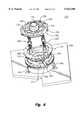
- the rotatable locking assembly 240includes a locking plate 260 to which the bottom portion of each spring pair 232 is attached and a lower ring portion 262 which can be seated and clamped within the wafer prober table 266 in a conventional fashion, using clamps 268.
- the locking assembly 240includes a ring portion 262 which, in one embodiment, has six V-shaped rollers 270, 272 (two fixed rollers 270 and four eccentric rollers 272).
- the V-shaped rollers 270, 272engage an internal V-groove in probe card holder ring 274 which fits into the wafer prober table recess 266. This arrangement permits accurate angular rotation of an affixed prober card 280 (as seen in FIG.
- FIG. 10shows a cross sectional view of the compliant wafer prober docking adapter 200 of FIG. 8.
- angular rotationif a prober card 280 contained within the locking assembly could be much higher (e.g., 180°), the 15° adjustment allows the ability for a user to accurately align the probe tips 290 of FIG. 10 to a wafer 292 (e.g., a substrate of a test board currently under evaluation).
- the combination of the fixed and eccentric rollers 270, 272 and a corresponding V-groove ring 274 within the wafer prober table 266allows for smooth and accurate angular rotation-of the locking assembly 240, which can then be locked in position by use of lock 284.
- the docking cone 220is affixed to the spider 222 of FIG. 8 and fixture board 210 in a manner previously described.
- the tapered or conical spring pairs 232(one pair can be seen in exploded view in FIG. 9) are interconnected between the fixture board arrangement 202 and locking assembly 240 of FIG. 8 in a similar manner.
- a pair of flexible electrical cables 300are electrically interconnected in a known manner between the fixture board arrangement 202 and the prober card 280, and hence to the prober tips 290.
- the use of the flexible electrical cables 300provides the necessary electrical interconnection between a test head and a test device 292.
- the present inventionprovides for a compliant wafer prober docking adapter 200 with desirable features and advantages which will now be described.
- FIG. 11shows another perspective view of the compliant wafer prober docking adapter 200 in which a pair of locking arms 310 , which when rotated by a user, serve to rotate the upper locking assembly 312 to engage and lock a test head (such as a test head 12 of FIG. 1).
- the inverted docking cone 220serves to facilitate the initial engagement of a test head 12 of FIG. 1 to the fixture board arrangement 202 of FIG. 8.
- the use of the compliant spring mechanism 230including tapered or conical spring pairs 232 provides a number of desirable features according to the present invention.
- the spring pairs 232compliantly adapt to the mass and rigidity of the test head itself
- the use of conical spring pairs 232provides a compliant adapter capability by providing both tension and compression. It is preferable to provide an adaptive compliance in all directions of approximately 1/4-5/16 inch.
- a usercould utilize a television camera 320, which when used with a prism (not shown), could provide an accurate display of the alignment process on a television monitor for greatly simplifying the docking process, as previously described above.
- the use of a television camera 320would permit viewing the alignment process from the side of the compliant adapter.
- a microscope(not shown) could be utilized with the compliant wafer prober docking adapter 200 shown in FIG. 8, or a user could simply view the alignment process directly through the aperture 218 in the inverted docking cone 220.
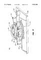
- FIG. 12shows a bottom isometric view of the compliant wafer prober docking adapter 200 according to the present invention.
- the compliant adapter 200can be seated within the recess within prober table 266.
- the fixed rollers 270 and eccentric rollers 272engage a V-groove 262 in ring 274 so as to facilitate the angular rotation of locking assembly 240, as previously described.
- a usercan view the alignment of the prober tips 290 of FIG. 10 to the test board, such as with a television camera, microscope, or by directly viewing the alignment through the viewing aperture 218.
- the handle 282can be rotated and locked by lock 284 such that the angular rotation range is within the preferred embodiment of 15° (other ranges can be provided, as necessary).
- the locked positionthus provides for a compliant adaptive capability which enables a single user to accurately and quickly align a docking system such as previously described.
- the compliant wafer prober docking adapter 200provides a compliant docking capability which permits a test head (such as test head 12 of FIG. 1) to be floated (to come down) to the top portion of the compliant adapter 200.
- the inverted docking cone 220has the top or first end which is narrower than the second or bottom end (the bottom end is wider than the top end). This arrangement facilitates the initial docking process of the test head to the fixture board arrangement 202.
- the coiled spring pairs 232compliantly support a portion of the weight of the test head and further the upper portion of the adapter 200 automatically aligns itself with the test head, as would be understood in viewing FIG. 11.
- the compliant adapter 200includes flexible cables 300 electrically interconnected in FIG. 10 between the two top and bottom surfaces and, in one embodiment, the compliance between the two surfaces is approximately 1/4-5/16 inch in all directions.
- the present inventionprovides for angular adjustment of a prober card 280 shown in FIG. 10, which allows for angular alignment of the prober tips 290 to a wafer 292 within approximately 15 degrees (in one embodiment).
- the present inventionallows for one user who can view the alignment process through a microscope 320 (or television monitor) without the complexity and awkwardness of prior art approaches.
- test headscan be easily moved from one wafer prober to another, because the alignment of the adapter 200 to a wafer 292 is not being disturbed. Hence, test heads can be moved back and forth between stations very quickly without having to go through another long and complex re-alignment process.
Landscapes
- Engineering & Computer Science (AREA)
- Computer Hardware Design (AREA)
- Microelectronics & Electronic Packaging (AREA)
- General Engineering & Computer Science (AREA)
- Physics & Mathematics (AREA)
- General Physics & Mathematics (AREA)
- Testing Or Measuring Of Semiconductors Or The Like (AREA)
- Testing Of Individual Semiconductor Devices (AREA)
- Measuring Leads Or Probes (AREA)
- Tests Of Electronic Circuits (AREA)
Abstract
Description
Claims (11)
Priority Applications (4)
| Application Number | Priority Date | Filing Date | Title |
|---|---|---|---|
| US08/794,821US5923180A (en) | 1997-02-04 | 1997-02-04 | Compliant wafer prober docking adapter |
| DE19752229ADE19752229C2 (en) | 1997-02-04 | 1997-11-25 | Compliant wafer tester coupling adapter |
| GB9801167AGB2323486B (en) | 1997-02-04 | 1998-01-20 | Compliant wafer prober docking adapter |
| JP10022456AJPH10223708A (en) | 1997-02-04 | 1998-02-04 | Obedient wafer-prober coupling adapter |
Applications Claiming Priority (1)
| Application Number | Priority Date | Filing Date | Title |
|---|---|---|---|
| US08/794,821US5923180A (en) | 1997-02-04 | 1997-02-04 | Compliant wafer prober docking adapter |
Publications (1)
| Publication Number | Publication Date |
|---|---|
| US5923180Atrue US5923180A (en) | 1999-07-13 |
Family
ID=25163780
Family Applications (1)
| Application Number | Title | Priority Date | Filing Date |
|---|---|---|---|
| US08/794,821Expired - Fee RelatedUS5923180A (en) | 1997-02-04 | 1997-02-04 | Compliant wafer prober docking adapter |
Country Status (4)
| Country | Link |
|---|---|
| US (1) | US5923180A (en) |
| JP (1) | JPH10223708A (en) |
| DE (1) | DE19752229C2 (en) |
| GB (1) | GB2323486B (en) |
Cited By (52)
| Publication number | Priority date | Publication date | Assignee | Title |
|---|---|---|---|---|
| US6114869A (en)* | 1998-05-21 | 2000-09-05 | Cerprobe Corporation | Method and apparatus for interfacing between automatic wafer probe machines, automatic testers, and probe cards |
| US6127818A (en)* | 1997-04-24 | 2000-10-03 | Sgs-Thomson Microelectronics S.A. | Tightening rings for integrated circuit tester heads |
| US6181148B1 (en)* | 1998-07-20 | 2001-01-30 | International Business Machines Corporation | Automated test head interface board locking and docking mechanism |
| US6255834B1 (en) | 1999-10-21 | 2001-07-03 | Dell Usa, L.P. | Test fixture having a floating self-centering connector |
| US6424167B1 (en)* | 2000-03-22 | 2002-07-23 | National Semiconductor Corporation | Vibration resistant test module for use with semiconductor device test apparatus |
| WO2002063315A1 (en)* | 2001-02-07 | 2002-08-15 | Teradyne, Inc. | Low profile pneumatically actuated docking module with power fault release |
| US6466044B1 (en) | 1999-10-21 | 2002-10-15 | Dell Products L.P. | Through connector circuit test apparatus |
| US20020172579A1 (en)* | 2001-05-07 | 2002-11-21 | Helmuth Heigl | Docking device, more particularly for a probe and a tester |
| US6570397B2 (en) | 2001-08-07 | 2003-05-27 | Agilent Technologies, Inc. | Timing calibration and timing calibration verification of electronic circuit testers |
| US20030102857A1 (en)* | 2001-12-03 | 2003-06-05 | Peter Hirschmann | Measuring and/or calibrating a test head |
| US20030122536A1 (en)* | 2001-12-29 | 2003-07-03 | Bin Mohamed Hassan Lokman | Docking system and method for docking in automated testing systems |
| US20040056675A1 (en)* | 2002-09-25 | 2004-03-25 | Advantest Corporation | Locking apparatus and loadboard assembly |
| US20040145383A1 (en)* | 2002-11-18 | 2004-07-29 | Matthias Brunner | Apparatus and method for contacting of test objects |
| US20040227532A1 (en)* | 2000-09-15 | 2004-11-18 | Orsillo James F. | Apparatus and method for use in testing a semiconductor wafer |
| US20040232927A1 (en)* | 2002-05-23 | 2004-11-25 | Gleason K. Reed | Probe for testing a device under test |
| US6833696B2 (en) | 2003-03-04 | 2004-12-21 | Xandex, Inc. | Methods and apparatus for creating a high speed connection between a device under test and automatic test equipment |
| US20050179452A1 (en)* | 2004-02-12 | 2005-08-18 | Applied Materials, Inc. | Configurable prober for TFT LCD array test |
| US20050179453A1 (en)* | 2004-02-12 | 2005-08-18 | Shinichi Kurita | Integrated substrate transfer module |
| US20050179451A1 (en)* | 2004-02-12 | 2005-08-18 | Applied Materials, Inc. | Configurable prober for TFT LCD array testing |
| EP1584934A1 (en)* | 2004-04-05 | 2005-10-12 | Agilent Technologies, Inc. | Device for releasable connecting an interface to a test equipment |
| US20060038554A1 (en)* | 2004-02-12 | 2006-02-23 | Applied Materials, Inc. | Electron beam test system stage |
| US20060244467A1 (en)* | 2005-04-29 | 2006-11-02 | Applied Materials, Inc. | In-line electron beam test system |
| US7233160B2 (en) | 2000-12-04 | 2007-06-19 | Cascade Microtech, Inc. | Wafer probe |
| US20070176615A1 (en)* | 2006-01-27 | 2007-08-02 | Xandex, Inc. | Active probe contact array management |
| US7271603B2 (en) | 2003-05-23 | 2007-09-18 | Cascade Microtech, Inc. | Shielded probe for testing a device under test |
| US20070216428A1 (en)* | 2006-03-14 | 2007-09-20 | Ralf Schmid | Method to reduce cross talk in a multi column e-beam test system |
| US7285969B2 (en) | 2002-11-13 | 2007-10-23 | Cascade Microtech, Inc. | Probe for combined signals |
| US20070296437A1 (en)* | 2006-05-31 | 2007-12-27 | Johnston Benjamin M | Mini-prober for tft-lcd testing |
| US20070296426A1 (en)* | 2006-05-31 | 2007-12-27 | Applied Materials, Inc. | Prober for electronic device testing on large area substrates |
| US7403028B2 (en) | 2006-06-12 | 2008-07-22 | Cascade Microtech, Inc. | Test structure and probe for differential signals |
| US7420381B2 (en) | 2004-09-13 | 2008-09-02 | Cascade Microtech, Inc. | Double sided probing structures |
| US7427868B2 (en) | 2003-12-24 | 2008-09-23 | Cascade Microtech, Inc. | Active wafer probe |
| US20080258712A1 (en)* | 2004-07-13 | 2008-10-23 | Intest Corporation | Modular interface |
| US7443186B2 (en) | 2006-06-12 | 2008-10-28 | Cascade Microtech, Inc. | On-wafer test structures for differential signals |
| US7449899B2 (en) | 2005-06-08 | 2008-11-11 | Cascade Microtech, Inc. | Probe for high frequency signals |
| US7504842B2 (en) | 1997-05-28 | 2009-03-17 | Cascade Microtech, Inc. | Probe holder for testing of a test device |
| US20090122056A1 (en)* | 2002-06-19 | 2009-05-14 | Akt Electron Beam Technology Gmbh | Drive apparatus with improved testing properties |
| US7535247B2 (en) | 2005-01-31 | 2009-05-19 | Cascade Microtech, Inc. | Interface for testing semiconductors |
| US20090237100A1 (en)* | 2005-11-15 | 2009-09-24 | Advantest Corporation | Electronic Device Test Apparatus and Method of Mounting of Performance Board in Electronic Device Test Apparatus |
| US7609077B2 (en) | 2006-06-09 | 2009-10-27 | Cascade Microtech, Inc. | Differential signal probe with integral balun |
| US20090267631A1 (en)* | 2008-04-24 | 2009-10-29 | Honeywell International Inc. | Large Component Thermal Head Adapter |
| US7619419B2 (en) | 2005-06-13 | 2009-11-17 | Cascade Microtech, Inc. | Wideband active-passive differential signal probe |
| US7656172B2 (en) | 2005-01-31 | 2010-02-02 | Cascade Microtech, Inc. | System for testing semiconductors |
| US7723999B2 (en) | 2006-06-12 | 2010-05-25 | Cascade Microtech, Inc. | Calibration structures for differential signal probing |
| US20100134134A1 (en)* | 2008-11-25 | 2010-06-03 | Verigy (Singapore) Pte. Ltd. | Test electronics to device under test interfaces, and methods and apparatus using same |
| US7764072B2 (en) | 2006-06-12 | 2010-07-27 | Cascade Microtech, Inc. | Differential signal probing system |
| US7876114B2 (en) | 2007-08-08 | 2011-01-25 | Cascade Microtech, Inc. | Differential waveguide probe |
| US9519023B2 (en) | 2012-05-03 | 2016-12-13 | Turbodynamics Gmbh | Module for exchanging an interface unit in a testing system for testing semiconductor components and testing system comprising such a module |
| CN113015913A (en)* | 2018-12-21 | 2021-06-22 | 株式会社友华 | Inspection jig support, and inspection jig |
| CN114049976A (en)* | 2021-11-18 | 2022-02-15 | 中国船舶重工集团公司第七一九研究所 | A multi-stage nuclear detection device |
| US11307112B2 (en)* | 2019-08-07 | 2022-04-19 | Qingdao university of technology | Simply-supported fixture used for circular plate in dynamics or statics experiment |
| CN115980398A (en)* | 2022-12-12 | 2023-04-18 | 北京华峰测控技术股份有限公司 | Connecting devices, setting methods, connectors and testing machines for floating interfaces |
Families Citing this family (7)
| Publication number | Priority date | Publication date | Assignee | Title |
|---|---|---|---|---|
| KR100707044B1 (en)* | 1999-05-27 | 2007-04-13 | 나노넥서스, 인코포레이티드 | Structure of integrated circuit wafer probe card assembly and its manufacturing method |
| KR100899121B1 (en)* | 2002-11-12 | 2009-05-26 | 한국항공우주산업 주식회사 | Interface Adapter for Calibration of Load Cells for Aircraft Weighing |
| DE102005057508B4 (en)* | 2005-12-01 | 2011-11-17 | Multitest Elektronische Systeme Gmbh | Docking device for coupling a handling device with a test head for electronic components |
| WO2011024295A1 (en)* | 2009-08-28 | 2011-03-03 | 株式会社アドバンテスト | Interface apparatus and semiconductor testing apparatus |
| DE102011014148B4 (en)* | 2011-03-16 | 2016-06-09 | Esmo Ag | Docking device |
| DE102013109055A1 (en) | 2013-08-21 | 2015-02-26 | Turbodynamics Gmbh | Alignment device and handling device |
| JP7138004B2 (en)* | 2018-09-28 | 2022-09-15 | 株式会社日本マイクロニクス | Probe card holder |
Citations (7)
| Publication number | Priority date | Publication date | Assignee | Title |
|---|---|---|---|---|
| US4893074A (en)* | 1988-05-13 | 1990-01-09 | Intest Corporation | Electronic device testing system |
| US5068601A (en)* | 1991-02-11 | 1991-11-26 | Credence Systems Corporation | Dual function cam-ring system for DUT board parallel electrical inter-connection and prober/handler docking |
| US5550466A (en)* | 1994-09-30 | 1996-08-27 | Hewlett-Packard Company | Hinged conduit for routing cables in an electronic circuit tester |
| US5552701A (en)* | 1995-05-15 | 1996-09-03 | Hewlett-Packard Company | Docking system for an electronic circuit tester |
| US5606262A (en)* | 1995-06-07 | 1997-02-25 | Teradyne, Inc. | Manipulator for automatic test equipment test head |
| US5663653A (en)* | 1992-06-11 | 1997-09-02 | Cascade Microtech, Inc. | Wafer probe station for low-current measurements |
| US5828225A (en)* | 1995-07-05 | 1998-10-27 | Tokyo Electron Limited | Semiconductor wafer probing apparatus |
Family Cites Families (1)
| Publication number | Priority date | Publication date | Assignee | Title |
|---|---|---|---|---|
| US4665360A (en)* | 1985-03-11 | 1987-05-12 | Eaton Corporation | Docking apparatus |
- 1997
- 1997-02-04USUS08/794,821patent/US5923180A/ennot_activeExpired - Fee Related
- 1997-11-25DEDE19752229Apatent/DE19752229C2/ennot_activeExpired - Fee Related
- 1998
- 1998-01-20GBGB9801167Apatent/GB2323486B/ennot_activeExpired - Fee Related
- 1998-02-04JPJP10022456Apatent/JPH10223708A/enactivePending
Patent Citations (7)
| Publication number | Priority date | Publication date | Assignee | Title |
|---|---|---|---|---|
| US4893074A (en)* | 1988-05-13 | 1990-01-09 | Intest Corporation | Electronic device testing system |
| US5068601A (en)* | 1991-02-11 | 1991-11-26 | Credence Systems Corporation | Dual function cam-ring system for DUT board parallel electrical inter-connection and prober/handler docking |
| US5663653A (en)* | 1992-06-11 | 1997-09-02 | Cascade Microtech, Inc. | Wafer probe station for low-current measurements |
| US5550466A (en)* | 1994-09-30 | 1996-08-27 | Hewlett-Packard Company | Hinged conduit for routing cables in an electronic circuit tester |
| US5552701A (en)* | 1995-05-15 | 1996-09-03 | Hewlett-Packard Company | Docking system for an electronic circuit tester |
| US5606262A (en)* | 1995-06-07 | 1997-02-25 | Teradyne, Inc. | Manipulator for automatic test equipment test head |
| US5828225A (en)* | 1995-07-05 | 1998-10-27 | Tokyo Electron Limited | Semiconductor wafer probing apparatus |
Cited By (114)
| Publication number | Priority date | Publication date | Assignee | Title |
|---|---|---|---|---|
| US6127818A (en)* | 1997-04-24 | 2000-10-03 | Sgs-Thomson Microelectronics S.A. | Tightening rings for integrated circuit tester heads |
| US7504842B2 (en) | 1997-05-28 | 2009-03-17 | Cascade Microtech, Inc. | Probe holder for testing of a test device |
| US6114869A (en)* | 1998-05-21 | 2000-09-05 | Cerprobe Corporation | Method and apparatus for interfacing between automatic wafer probe machines, automatic testers, and probe cards |
| US6181148B1 (en)* | 1998-07-20 | 2001-01-30 | International Business Machines Corporation | Automated test head interface board locking and docking mechanism |
| US6255834B1 (en) | 1999-10-21 | 2001-07-03 | Dell Usa, L.P. | Test fixture having a floating self-centering connector |
| US6466044B1 (en) | 1999-10-21 | 2002-10-15 | Dell Products L.P. | Through connector circuit test apparatus |
| US6424167B1 (en)* | 2000-03-22 | 2002-07-23 | National Semiconductor Corporation | Vibration resistant test module for use with semiconductor device test apparatus |
| US7053646B2 (en)* | 2000-09-15 | 2006-05-30 | Orsillo James F | Apparatus and method for use in testing a semiconductor wafer |
| US20040227532A1 (en)* | 2000-09-15 | 2004-11-18 | Orsillo James F. | Apparatus and method for use in testing a semiconductor wafer |
| US6551122B2 (en) | 2000-10-04 | 2003-04-22 | Teradyne, Inc. | Low profile pneumatically actuated docking module with power fault release |
| US7761983B2 (en) | 2000-12-04 | 2010-07-27 | Cascade Microtech, Inc. | Method of assembling a wafer probe |
| US7495461B2 (en) | 2000-12-04 | 2009-02-24 | Cascade Microtech, Inc. | Wafer probe |
| US7233160B2 (en) | 2000-12-04 | 2007-06-19 | Cascade Microtech, Inc. | Wafer probe |
| US7688097B2 (en) | 2000-12-04 | 2010-03-30 | Cascade Microtech, Inc. | Wafer probe |
| US7456646B2 (en) | 2000-12-04 | 2008-11-25 | Cascade Microtech, Inc. | Wafer probe |
| WO2002063315A1 (en)* | 2001-02-07 | 2002-08-15 | Teradyne, Inc. | Low profile pneumatically actuated docking module with power fault release |
| KR100853664B1 (en) | 2001-02-07 | 2008-08-25 | 테라다인 인코퍼레이티드 | Thin docking module operated by air pressure and released in case of power failure |
| US20020172579A1 (en)* | 2001-05-07 | 2002-11-21 | Helmuth Heigl | Docking device, more particularly for a probe and a tester |
| US6844718B2 (en)* | 2001-05-07 | 2005-01-18 | Helmuth Heigl | Docking device, more particularly for a probe and a tester |
| US6570397B2 (en) | 2001-08-07 | 2003-05-27 | Agilent Technologies, Inc. | Timing calibration and timing calibration verification of electronic circuit testers |
| US20030102857A1 (en)* | 2001-12-03 | 2003-06-05 | Peter Hirschmann | Measuring and/or calibrating a test head |
| US6756778B2 (en)* | 2001-12-03 | 2004-06-29 | Agilent Technologies, Inc. | Measuring and/or calibrating a test head |
| US6897645B2 (en)* | 2001-12-29 | 2005-05-24 | Vincent Hing Chung So | Docking system and method for docking in automated testing systems |
| US20030122536A1 (en)* | 2001-12-29 | 2003-07-03 | Bin Mohamed Hassan Lokman | Docking system and method for docking in automated testing systems |
| US7436194B2 (en) | 2002-05-23 | 2008-10-14 | Cascade Microtech, Inc. | Shielded probe with low contact resistance for testing a device under test |
| US7489149B2 (en) | 2002-05-23 | 2009-02-10 | Cascade Microtech, Inc. | Shielded probe for testing a device under test |
| US7304488B2 (en) | 2002-05-23 | 2007-12-04 | Cascade Microtech, Inc. | Shielded probe for high-frequency testing of a device under test |
| US7482823B2 (en) | 2002-05-23 | 2009-01-27 | Cascade Microtech, Inc. | Shielded probe for testing a device under test |
| US20040232927A1 (en)* | 2002-05-23 | 2004-11-25 | Gleason K. Reed | Probe for testing a device under test |
| US7518387B2 (en) | 2002-05-23 | 2009-04-14 | Cascade Microtech, Inc. | Shielded probe for testing a device under test |
| US7161363B2 (en) | 2002-05-23 | 2007-01-09 | Cascade Microtech, Inc. | Probe for testing a device under test |
| US8208114B2 (en) | 2002-06-19 | 2012-06-26 | Akt Electron Beam Technology Gmbh | Drive apparatus with improved testing properties |
| US20090122056A1 (en)* | 2002-06-19 | 2009-05-14 | Akt Electron Beam Technology Gmbh | Drive apparatus with improved testing properties |
| US6747447B2 (en)* | 2002-09-25 | 2004-06-08 | Advantest Corporation | Locking apparatus and loadboard assembly |
| US20040056675A1 (en)* | 2002-09-25 | 2004-03-25 | Advantest Corporation | Locking apparatus and loadboard assembly |
| US7285969B2 (en) | 2002-11-13 | 2007-10-23 | Cascade Microtech, Inc. | Probe for combined signals |
| US7417446B2 (en) | 2002-11-13 | 2008-08-26 | Cascade Microtech, Inc. | Probe for combined signals |
| US7453276B2 (en) | 2002-11-13 | 2008-11-18 | Cascade Microtech, Inc. | Probe for combined signals |
| US7135875B2 (en) | 2002-11-18 | 2006-11-14 | Applied Materials Gmbh | Apparatus and method for contacting of test objects |
| US20060181290A1 (en)* | 2002-11-18 | 2006-08-17 | Applied Materials, Inc. (Gmbh) | Apparatus and method for contacting of test objects |
| US20040145383A1 (en)* | 2002-11-18 | 2004-07-29 | Matthias Brunner | Apparatus and method for contacting of test objects |
| US7474108B2 (en) | 2002-11-18 | 2009-01-06 | Applied Materials, Gmbh | Apparatus and method for contacting of test objects |
| US6963211B2 (en) | 2003-03-04 | 2005-11-08 | Xandex, Inc. | Methods and apparatus for creating a high speed connection between a device under test and automatic test equipment |
| US20050264311A1 (en)* | 2003-03-04 | 2005-12-01 | Xandex, Inc. | Methods and apparatus for creating a high speed connection between a device under test and automatic test equipment |
| US20060244471A1 (en)* | 2003-03-04 | 2006-11-02 | Xandex, Inc. | Methods and apparatus for creating a high speed connection between a device under test and automatic test equipment |
| US7078890B2 (en) | 2003-03-04 | 2006-07-18 | Xandex, Inc. | Methods and apparatus for creating a high speed connection between a device under test and automatic test equipment |
| US7358754B2 (en) | 2003-03-04 | 2008-04-15 | Xandex, Inc. | Methods and apparatus for creating a high speed connection between a device under test and automatic test equipment |
| US20050046411A1 (en)* | 2003-03-04 | 2005-03-03 | Xandex, Inc. | Methods and apparatus for creating a high speed connection between a device under test and automatic test equipment |
| US20070126439A1 (en)* | 2003-03-04 | 2007-06-07 | Xandex, Inc. | Methods and apparatus for creating a high speed connection between a device under test and automatic test equipment |
| US6833696B2 (en) | 2003-03-04 | 2004-12-21 | Xandex, Inc. | Methods and apparatus for creating a high speed connection between a device under test and automatic test equipment |
| US7898273B2 (en) | 2003-05-23 | 2011-03-01 | Cascade Microtech, Inc. | Probe for testing a device under test |
| US7501842B2 (en) | 2003-05-23 | 2009-03-10 | Cascade Microtech, Inc. | Shielded probe for testing a device under test |
| US7271603B2 (en) | 2003-05-23 | 2007-09-18 | Cascade Microtech, Inc. | Shielded probe for testing a device under test |
| US7498829B2 (en) | 2003-05-23 | 2009-03-03 | Cascade Microtech, Inc. | Shielded probe for testing a device under test |
| US7427868B2 (en) | 2003-12-24 | 2008-09-23 | Cascade Microtech, Inc. | Active wafer probe |
| US7759953B2 (en) | 2003-12-24 | 2010-07-20 | Cascade Microtech, Inc. | Active wafer probe |
| US20080111577A1 (en)* | 2004-02-12 | 2008-05-15 | Shinichi Kurita | Integrated Substrate Transfer Module |
| US7919972B2 (en) | 2004-02-12 | 2011-04-05 | Applied Materials, Inc. | Integrated substrate transfer module |
| US7355418B2 (en) | 2004-02-12 | 2008-04-08 | Applied Materials, Inc. | Configurable prober for TFT LCD array test |
| US20060038554A1 (en)* | 2004-02-12 | 2006-02-23 | Applied Materials, Inc. | Electron beam test system stage |
| US20080061807A1 (en)* | 2004-02-12 | 2008-03-13 | Matthias Brunner | Configurable Prober for TFT LCD Array Test |
| US7330021B2 (en) | 2004-02-12 | 2008-02-12 | Applied Materials, Inc. | Integrated substrate transfer module |
| US20050179451A1 (en)* | 2004-02-12 | 2005-08-18 | Applied Materials, Inc. | Configurable prober for TFT LCD array testing |
| US7319335B2 (en) | 2004-02-12 | 2008-01-15 | Applied Materials, Inc. | Configurable prober for TFT LCD array testing |
| US20050179453A1 (en)* | 2004-02-12 | 2005-08-18 | Shinichi Kurita | Integrated substrate transfer module |
| US7847566B2 (en) | 2004-02-12 | 2010-12-07 | Applied Materials, Inc. | Configurable prober for TFT LCD array test |
| US20050179452A1 (en)* | 2004-02-12 | 2005-08-18 | Applied Materials, Inc. | Configurable prober for TFT LCD array test |
| EP1584934A1 (en)* | 2004-04-05 | 2005-10-12 | Agilent Technologies, Inc. | Device for releasable connecting an interface to a test equipment |
| US20050264278A1 (en)* | 2004-04-05 | 2005-12-01 | Agilent Technologies, Inc. | Device for releasable connecting an interface with a test equipment |
| US7164278B2 (en) | 2004-04-05 | 2007-01-16 | Agilent Technologies, Inc. | Device for releasable connecting an interface with a test equipment |
| US20080258712A1 (en)* | 2004-07-13 | 2008-10-23 | Intest Corporation | Modular interface |
| US20080258713A1 (en)* | 2004-07-13 | 2008-10-23 | Intest Corporation | Modular interface |
| US7605582B2 (en)* | 2004-07-13 | 2009-10-20 | Intest Corporation | Modular interface |
| US7605583B2 (en)* | 2004-07-13 | 2009-10-20 | Intest Corporation | Modular interface |
| US8013623B2 (en) | 2004-09-13 | 2011-09-06 | Cascade Microtech, Inc. | Double sided probing structures |
| US7420381B2 (en) | 2004-09-13 | 2008-09-02 | Cascade Microtech, Inc. | Double sided probing structures |
| US7656172B2 (en) | 2005-01-31 | 2010-02-02 | Cascade Microtech, Inc. | System for testing semiconductors |
| US7898281B2 (en) | 2005-01-31 | 2011-03-01 | Cascade Mircotech, Inc. | Interface for testing semiconductors |
| US7940069B2 (en) | 2005-01-31 | 2011-05-10 | Cascade Microtech, Inc. | System for testing semiconductors |
| US7535247B2 (en) | 2005-01-31 | 2009-05-19 | Cascade Microtech, Inc. | Interface for testing semiconductors |
| US20060244467A1 (en)* | 2005-04-29 | 2006-11-02 | Applied Materials, Inc. | In-line electron beam test system |
| US20090195262A1 (en)* | 2005-04-29 | 2009-08-06 | Abboud Fayez E | In-line electron beam test system |
| US7535238B2 (en) | 2005-04-29 | 2009-05-19 | Applied Materials, Inc. | In-line electron beam test system |
| US7746088B2 (en) | 2005-04-29 | 2010-06-29 | Applied Materials, Inc. | In-line electron beam test system |
| US7449899B2 (en) | 2005-06-08 | 2008-11-11 | Cascade Microtech, Inc. | Probe for high frequency signals |
| US7619419B2 (en) | 2005-06-13 | 2009-11-17 | Cascade Microtech, Inc. | Wideband active-passive differential signal probe |
| US20090237100A1 (en)* | 2005-11-15 | 2009-09-24 | Advantest Corporation | Electronic Device Test Apparatus and Method of Mounting of Performance Board in Electronic Device Test Apparatus |
| US8013624B2 (en) | 2005-11-15 | 2011-09-06 | Advantest Corporation | Electronic device test apparatus and method of mounting of performance board in electronic device test apparatus |
| US8710855B2 (en) | 2005-11-15 | 2014-04-29 | Advantest Corporation | Probe card holding apparatus with probe card engagement structure |
| US20080030211A1 (en)* | 2006-01-27 | 2008-02-07 | Xandex, Inc. | Active probe contact array management |
| US20080030213A1 (en)* | 2006-01-27 | 2008-02-07 | Xandex, Inc. | Active probe contact array management |
| US20080030212A1 (en)* | 2006-01-27 | 2008-02-07 | Xandex, Inc. | Active probe contact array management |
| US20070176615A1 (en)* | 2006-01-27 | 2007-08-02 | Xandex, Inc. | Active probe contact array management |
| US20070216428A1 (en)* | 2006-03-14 | 2007-09-20 | Ralf Schmid | Method to reduce cross talk in a multi column e-beam test system |
| US7569818B2 (en) | 2006-03-14 | 2009-08-04 | Applied Materials, Inc. | Method to reduce cross talk in a multi column e-beam test system |
| US20070296426A1 (en)* | 2006-05-31 | 2007-12-27 | Applied Materials, Inc. | Prober for electronic device testing on large area substrates |
| US7786742B2 (en) | 2006-05-31 | 2010-08-31 | Applied Materials, Inc. | Prober for electronic device testing on large area substrates |
| US20070296437A1 (en)* | 2006-05-31 | 2007-12-27 | Johnston Benjamin M | Mini-prober for tft-lcd testing |
| US7602199B2 (en) | 2006-05-31 | 2009-10-13 | Applied Materials, Inc. | Mini-prober for TFT-LCD testing |
| US7609077B2 (en) | 2006-06-09 | 2009-10-27 | Cascade Microtech, Inc. | Differential signal probe with integral balun |
| US7443186B2 (en) | 2006-06-12 | 2008-10-28 | Cascade Microtech, Inc. | On-wafer test structures for differential signals |
| US7723999B2 (en) | 2006-06-12 | 2010-05-25 | Cascade Microtech, Inc. | Calibration structures for differential signal probing |
| US7764072B2 (en) | 2006-06-12 | 2010-07-27 | Cascade Microtech, Inc. | Differential signal probing system |
| US7750652B2 (en) | 2006-06-12 | 2010-07-06 | Cascade Microtech, Inc. | Test structure and probe for differential signals |
| US7403028B2 (en) | 2006-06-12 | 2008-07-22 | Cascade Microtech, Inc. | Test structure and probe for differential signals |
| US7876114B2 (en) | 2007-08-08 | 2011-01-25 | Cascade Microtech, Inc. | Differential waveguide probe |
| US20090267631A1 (en)* | 2008-04-24 | 2009-10-29 | Honeywell International Inc. | Large Component Thermal Head Adapter |
| US8354853B2 (en)* | 2008-11-25 | 2013-01-15 | Advantest (Singapore) Pte Ltd | Test electronics to device under test interfaces, and methods and apparatus using same |
| US20100134134A1 (en)* | 2008-11-25 | 2010-06-03 | Verigy (Singapore) Pte. Ltd. | Test electronics to device under test interfaces, and methods and apparatus using same |
| US9519023B2 (en) | 2012-05-03 | 2016-12-13 | Turbodynamics Gmbh | Module for exchanging an interface unit in a testing system for testing semiconductor components and testing system comprising such a module |
| CN113015913A (en)* | 2018-12-21 | 2021-06-22 | 株式会社友华 | Inspection jig support, and inspection jig |
| US11307112B2 (en)* | 2019-08-07 | 2022-04-19 | Qingdao university of technology | Simply-supported fixture used for circular plate in dynamics or statics experiment |
| CN114049976A (en)* | 2021-11-18 | 2022-02-15 | 中国船舶重工集团公司第七一九研究所 | A multi-stage nuclear detection device |
| CN115980398A (en)* | 2022-12-12 | 2023-04-18 | 北京华峰测控技术股份有限公司 | Connecting devices, setting methods, connectors and testing machines for floating interfaces |
Also Published As
| Publication number | Publication date |
|---|---|
| DE19752229C2 (en) | 2003-11-27 |
| GB9801167D0 (en) | 1998-03-18 |
| GB2323486B (en) | 2001-07-04 |
| GB2323486A (en) | 1998-09-23 |
| DE19752229A1 (en) | 1998-08-06 |
| JPH10223708A (en) | 1998-08-21 |
Similar Documents
| Publication | Publication Date | Title |
|---|---|---|
| US5923180A (en) | Compliant wafer prober docking adapter | |
| US5552701A (en) | Docking system for an electronic circuit tester | |
| US6476628B1 (en) | Semiconductor parallel tester | |
| US5068601A (en) | Dual function cam-ring system for DUT board parallel electrical inter-connection and prober/handler docking | |
| US5966023A (en) | Rapid action engagement interface connection system | |
| US6447339B1 (en) | Adapter for a multi-channel signal probe | |
| US5539305A (en) | Calibration board for an electronic circuit tester | |
| US6781391B2 (en) | Multi-channel, low input capacitance signal probe and probe head | |
| US5688127A (en) | Universal contactor system for testing ball grid array (BGA) devices on multiple handlers and method therefor | |
| US6970006B2 (en) | Apparatus for the automated testing, calibration and characterization of test adapters | |
| US20030077932A1 (en) | Floating blind mate interface for automatic test system | |
| US7420381B2 (en) | Double sided probing structures | |
| KR100428782B1 (en) | Apparatus for measuring tension of pogo pin | |
| US6636058B2 (en) | Adapter for a multi-channel, low input capacitance signal probe | |
| US20060214679A1 (en) | Active diagnostic interface for wafer probe applications | |
| US6741072B2 (en) | Docking system for connecting a tester to a probe station using an A-type docking configuration | |
| JPH1019960A (en) | Translator fixing unit for testing printed wiring board | |
| US7145352B2 (en) | Apparatus, method, and kit for probing a pattern of points on a printed circuit board | |
| JPS62502062A (en) | Electronic unit measuring device | |
| KR19990074916A (en) | Wafer testing equipment | |
| JP2008128798A (en) | Semiconductor test equipment | |
| WO1982002286A1 (en) | Multipin coupler | |
| JPH0353176A (en) | Package checking device | |
| JPS62121377A (en) | Test head jig |
Legal Events
| Date | Code | Title | Description |
|---|---|---|---|
| AS | Assignment | Owner name:HEWLETT-PACKARD COMPANY, CALIFORNIA Free format text:ASSIGNMENT OF ASSIGNORS INTEREST;ASSIGNORS:BOTKA, JULIUS K.;VETERAN, DAVID R.;REEL/FRAME:008515/0271 Effective date:19970321 | |
| AS | Assignment | Owner name:HEWLETT-PACKARD COMPANY, A DELAWARE CORPORATION, C Free format text:MERGER;ASSIGNOR:HEWLETT-PACKARD COMPANY, A CALIFORNIA CORPORATION;REEL/FRAME:010841/0649 Effective date:19980520 | |
| AS | Assignment | Owner name:AGILENT TECHNOLOGIES INC, CALIFORNIA Free format text:ASSIGNMENT OF ASSIGNORS INTEREST;ASSIGNOR:HEWLETT-PACKARD COMPANY;REEL/FRAME:010977/0540 Effective date:19991101 | |
| FEPP | Fee payment procedure | Free format text:PAYOR NUMBER ASSIGNED (ORIGINAL EVENT CODE: ASPN); ENTITY STATUS OF PATENT OWNER: LARGE ENTITY | |
| FPAY | Fee payment | Year of fee payment:4 | |
| FPAY | Fee payment | Year of fee payment:8 | |
| REMI | Maintenance fee reminder mailed | ||
| LAPS | Lapse for failure to pay maintenance fees | ||
| STCH | Information on status: patent discontinuation | Free format text:PATENT EXPIRED DUE TO NONPAYMENT OF MAINTENANCE FEES UNDER 37 CFR 1.362 | |
| FP | Lapsed due to failure to pay maintenance fee | Effective date:20110713 |