US5923178A - Probe assembly and method for switchable multi-DUT testing of integrated circuit wafers - Google Patents
Probe assembly and method for switchable multi-DUT testing of integrated circuit wafersDownload PDFInfo
- Publication number
- US5923178A US5923178AUS08/837,399US83739997AUS5923178AUS 5923178 AUS5923178 AUS 5923178AUS 83739997 AUS83739997 AUS 83739997AUS 5923178 AUS5923178 AUS 5923178A
- Authority
- US
- United States
- Prior art keywords
- probe
- contact
- needle
- wafer
- tip
- Prior art date
- Legal status (The legal status is an assumption and is not a legal conclusion. Google has not performed a legal analysis and makes no representation as to the accuracy of the status listed.)
- Expired - Lifetime
Links
Images


Classifications
- G—PHYSICS
- G01—MEASURING; TESTING
- G01R—MEASURING ELECTRIC VARIABLES; MEASURING MAGNETIC VARIABLES
- G01R31/00—Arrangements for testing electric properties; Arrangements for locating electric faults; Arrangements for electrical testing characterised by what is being tested not provided for elsewhere
- G01R31/28—Testing of electronic circuits, e.g. by signal tracer
- G01R31/282—Testing of electronic circuits specially adapted for particular applications not provided for elsewhere
- G01R31/2831—Testing of materials or semi-finished products, e.g. semiconductor wafers or substrates
- G—PHYSICS
- G01—MEASURING; TESTING
- G01R—MEASURING ELECTRIC VARIABLES; MEASURING MAGNETIC VARIABLES
- G01R1/00—Details of instruments or arrangements of the types included in groups G01R5/00 - G01R13/00 and G01R31/00
- G01R1/02—General constructional details
- G01R1/06—Measuring leads; Measuring probes
- G01R1/067—Measuring probes
- G01R1/073—Multiple probes
- G01R1/07307—Multiple probes with individual probe elements, e.g. needles, cantilever beams or bump contacts, fixed in relation to each other, e.g. bed of nails fixture or probe card
- G01R1/07357—Multiple probes with individual probe elements, e.g. needles, cantilever beams or bump contacts, fixed in relation to each other, e.g. bed of nails fixture or probe card with flexible bodies, e.g. buckling beams
Definitions
- the inventionrelates to wafer probe assemblies and methods for reducing "scrubbing" of wafer probe needle tips on bonding pads of an integrated circuit device under test (DUT), and especially to improvements therein which avoid “interference” between probe needles to thereby facilitate simultaneous probing of multiple die on the same semiconductor wafer to thereby reduce the number of "touch downs” of the probe needles required to probe test the entire semiconductor wafer.
- DUTintegrated circuit device under test
- the wafer chuckis raised approximately 3 mils so that the typically inclined probe needles "scrub" through brittle insulative aluminum oxide on the aluminum bonding pads to allow good mechanical and electrical contact of the needle tip with the bonding pad metal and thereby ensure low probe contact resistance.
- the wafer chuckcan be stationary and the test head can be moved).
- the probe needleseach need to apply at least approximately 3-15 grams of force against the bonding pad surfaces. That is, reliable probe needle contact to the bonding pad may require the tip of each needle to contact the aluminum bonding pad with a force in the range of 3-15 grams to effectively accomplish the necessary scrubbing.
- Such scrubbingmay involve "scratching" the bonding pad surface through a distance of roughly 0.5 to 1.5 mils while maintaining the 3-15 gram force on the probe needle in order to achieve reliable low resistance electrical contact between the probe needle and the aluminum metal of the bonding pad.
- FIG. 6shows a typical prior art cantilevered probe needle 14 that is inclined relative to the surface of aluminum bonding pad 62.
- Wafer 20is supported on wafer chuck 54, which is raised as indicated by arrow 22 through a distance of approximately 3 mils to achieve contact of the needle tip with bonding pad 62.
- Probe needle 14is sufficiently elastic or “compliant" to compensate for planarity (non-flatness) of the surface of semiconductor 20 and yet allow probe needle 14 to maintain the 3-15 gram force as it slides along and thereby scrubs aside the insulative aluminum oxide on the surface of aluminum bonding pad 62.
- the "scrub distance"is indicated by numeral 63, and typically is roughly 0.5 to 1.5 mils for many state-of-the-art wafer probe test systems.
- FIG. 7illustrates several common configurations of bonding pads on various types of semiconductor die 20, identified herein as "type I", “type II", or “type III”.
- the bonding pads 62usually are in the range of roughly 2-4 mils square, with pitch (center-to-center spacing) in the range of 4 to 10 mils.
- a single column (or row) of bonding pads 62may be provided as shown, so as to "bisect" the die 20.
- This bonding pad arrangementis most suitable for "multi-DUT wafer probing", wherein a single “touch down” of probe needles on corresponding bonding pads results in testing of multiple DUTs (die) on the wafer being probe tested.
- Type II bonding pad layoutscan include opposed parallel columns of bonding pads located along opposite edges of each chip, in which case multi-DUT wafer probing can be achieved by contacting bonding pads 62-1 on die 20 and the adjacent column of bonding pads 62-2 on die 21.
- a type II bonding pad arrangementcan include two closely spaced columns of bonding pads 62-1 and 62-2 centered on die 20.
- Type III bonding pad layouts, in which bonding pads 62 are positioned along all four edges of the die,are least well suited to multi-DUT testing.
- BCFbalanced contact force
- One known technique of making a probe cardis to provide a layer of copper or gold plated copper on one surface of a thin layer of polyimide insulator and to provide a pattern of nickel alloy strips on the other face of the polyimide layer.
- the nickel alloy stripsextend beyond one edge of the polyimide layer and form the probe needles, as shown in the above mentioned Higgins and Higgins et al. patents.
- the portions of the nickel alloy strips on the surface of the polyimide layercoact with the copper plating to function as 50 ohm transmission lines. This permits very high frequency test signals to be reliably transmitted between the probe test system and the bonding pads of the DUT.
- FIG. 8 hereofillustrates a known probe system referred to as the "Cobra" system, in which the upper ends of probe needles 14 are guided through a rigid layer 67 of insulating material, whereat the upper ends of the individual probe needles 14 are electrically connected to suitable conductors of an interface assembly that is connected to an electrical test system.
- Each of the needles 14 in FIG. 8is curved as illustrated and the lower end passes through a corresponding clearance hole 70 in a lower rigid layer or template 68 of insulating material.
- the bottom ends of the needles 14contact the bonding pads 62 of the wafer 20 being tested. Any "scrubbing" of the lower tips of probe needles 14 on the bonding pads 62 occurs as a result of looseness of the end 14A in the clearance holes 70.
- scrubbingrefers to substantial sliding of a probe needle tip on a bonding pad, e.g., about 0.5 mils or more, and excludes “micro-scrubbing” in which there is some but much less than 0.5 mils of sliding, scratching, or rubbing of the probe needle tip on the bonding pad.
- ground bouncenoise can be reduced by connecting "ground bounce” capacitors to the ground conductors as close as possible to the ground probe needle.
- ground supply conductor connected to the probe needle supplying a ground voltage to the DUThas been connected to a ground plane conductor on the printed circuit board of the assembly, and the power supply conductor connected to the probe needle supplying a power supply voltage to the DUT has been connected to a bypass capacitor connected to the ground plane on the printed circuit board. The substantial length of these two conductors has resulted in undesirable levels of ground noise and power supply noise being applied to the DUT during testing.
- the inventionprovides an apparatus for testing an integrated circuit on a semiconductor wafer so as to achieve low probe needle contact resistance with low probe needle force and without substantial scrubbing, including a probe assembly supporting a plurality of probe needles electrically coupled to an electrical test system above and having contact tips in alignment with a plurality of contact pads of the integrated circuit, respectively, each needle having a curved portion, a mechanical translating device operative to mechanically displace the wafer relative to the probe needles to bring a tip of each probe needle into physical contact with a corresponding contact pad, and to further mechanically displace the wafer against the probe needles to increase the needle force of each tip against the corresponding contact pad and thereby cause flexing of a curved portion of each probe needle.
- the curved portion of each needlehas a curvature such that the flexing causes the tip of each probe needle to rock on the insulative oxide coating on the contact pad without sliding through a substantial distance on the surface of the corresponding pad.
- the rocking and the needle forcecauses lateral displacement of oxide from between the contact tip of the probe needle and metal of the contact pad to provide reliable, low resistance electrical contact between the contact tip and the corresponding contact pad.
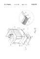
- FIG. 1Ais a perspective view of a probe contact array assembly according to a first embodiment of the present invention.
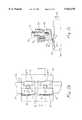
- FIG. 1Bis a top plan view diagram of a portion of a wafer probe assembly including two of the probe contact array assemblies of FIG. 1A arranged to accomplish multi-DUT testing.
- FIG. 1Cis a section view along section line 1C--1C of FIG. 1B.
- FIG. 2Ais a perspective view of a portion of a probe contact array assembly of a second embodiment of the invention.
- FIG. 2Bis a perspective view of a variation of the second embodiment of the structure shown in FIG. 2A, supporting two "probe contact arrays" and probe needles thereof.
- FIG. 2Cis a partial side section view illustrating the use of two of the embodiments of FIG. 2B to probe adjacent die on a semiconductor wafer.
- FIG. 2Dis a section view of a "probe contact array" used in the wafer probe apparatus of the invention.
- FIG. 2Eis a section view diagram illustrating connection of probe contact arrays to conductors of a printed circuit board in a probe test head by means of flex circuits.
- FIG. 2Fis a partial plan view of a probe contact array illustrating a via connecting a ground conductor to a ground plane, and also illustrating a power supply bypass capacitor connected adjacent to the edge of a ground plane of the probe contact array.
- FIG. 2Gis a partial side elevation view illustrating probe needle contact tip rotation displacing aluminum oxide due to flexing of the probe needle during a "touch down" onto an aluminum bonding pad of an integrated circuit under test.
- FIG. 3is a perspective diagram of a portion of a probe assembly of a third embodiment of the invention.
- FIG. 3Ais a modified section view across section line 3A--3A of FIG. 3 showing use of "layered" probe contact arrays to accomplish testing of integrated circuit arrays.
- FIG. 3Bis a partial perspective diagram useful in explaining how the apparatus of FIG. 3 can be extended to multi-DUT testing of die having "type III" bonding pad locations.
- FIG. 4is a top plan view diagram of a probe assembly including a printed circuit board supporting two probe contact array assemblies of FIG. 2B and a support plate for the printed circuit board.
- FIG. 4Ais a section view along section line 4A--4A of FIG. 4.
- FIG. 4Bis a section view along section 4B--4B of FIG. 4.
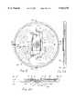
- FIG. 5is a plan view diagram of a semiconductor wafer mounted on a chuck, indicating a multi-DUT testing pattern, and also illustrating other components of a wafer probe test system.
- FIG. 6is a partial section view diagram useful in describing the prior art.
- FIG. 7is a diagram identifying different types of bonding pad arrangements on integrated circuits.
- FIG. 8is a partial section view diagram useful in describing the prior art.
- FIG. 9is a partial perspective view of an alternative embodiment of the invention.
- the term "scrubbing" as used hereinis intended to refer to a substantial lateral scraping, scratching, or rubbing movement through a distance of roughly 0.5-1.5 mils by the contact tip of a probe needle against the surface of a bonding pad or other contact pad of an integrated circuit die, to penetrate through the brittle insulative oxide on the pad metal to achieve reliable electrical contact between the probe needle contact tip and the pad metal, with low needle force against the probe.
- scrubbingas used herein is in contrast to and exclusive of "micro-scrubbing” or “rocking” movements of the contacting tip of the probe needle on the integrated circuit bonding pads wherein there is much less than 0.5 to 1.5 mils of lateral movement of the contacting tip of the probe needle against the surface of the bonding pad.
- a "test head”carries an “interface assembly” which in turn carries a probe assembly.
- Each probe assemblycarries enough probe needles to effectuate testing of one or more integrated circuit die.
- probe assemblyas used hereinafter is intended to include the combination of
- PCBprinted circuit board
- probe contact array assemblyincluding (i) one or more "probe contact arrays” of probe needles to effectuate complete testing of one or more integrated circuit die (DUT), and (ii) a "flex circuit” or “tail” interconnection for electrically coupling each probe needle of the contact array(s) to a corresponding conductor of the printed circuit board, and
- the mechanical mounting assemblyis capable of performing both a positioning function and an attachment function, so as to achieve alignment of the needle of the probe contact array with a corresponding DUT and also achieve the compliance of the probe needle contact tips necessary to account for variations in the planarity of the semiconductor wafer so that each probe needle contact tip makes electrical contact with a force in the range of roughly 1-12 grams against the intended bonding pads of the DUT or multiple DUTs.
- a typical "interface assembly”includes a number of gold plated spring loaded telescoping "POGO pins". When the interface assembly is "brought down” on a probe card assembly, the spring loaded POGO pins collapse a bit and make the needed contact between contact pads of the printed circuit board and the test head, which is connected to the test system.
- FIGS. 1A-1CA first embodiment of the invention is shown in FIGS. 1A-1C and includes a "probe contact array assembly" 10 including a plated probe contact array 40 and a mounting assembly 11.
- Plated probe contact array 40has the structure described above with reference to FIG. 2D, and includes an array of plated nickel alloy probe needles 14 extending therefrom.
- the probe contact array 40is attached to the lower surface of a cantilever-mounted leaf spring 12, which is rigidly affixed at one end to a bottom surface of mounting assembly 11.
- each of the individual probe needles 14has a bent outer contact tip 14C which, during testing of the wafer, electrically contacts a corresponding bonding or contact pad 62 of an integrated circuit die 21 of a semiconductor wafer that also includes hundreds of other such integrated circuit die.
- the contact tips of the probe needles 14are tapered from 2 to 4 mil width "shanks" on the probe contact array down to 0.5 to 2 mil width contact tips for contacting the bonding or contact pads or the solder bumps of the DUT.
- Mounting assembly 11includes a lower base section 11B to which one end of leaf spring 12 is rigidly attached.
- the precise position of lower base section 11B relative to upper section 11A of mounting assembly 11is determined by a set screw 16 extending through a threaded hole in upper section 11A to abut a horizontal upper surface of base section 11B.
- Set screws 17perform the same function.
- a shoulder bolt 15extends through a clearance hole in the upper surface of upper section 11A and is threaded into a hole in lower section 11B.
- a compression spring 23is disposed about the shaft of bolt 15 between the shoulder thereof and the upper surface of upper section 11A to maintain a suitable bias force downward on lower section 11A.
- one or more probe contact array assemblies 10can be attached to a printed circuit board by means of a continuous "bridge" 11C that constitutes an extension of the upper section 11A of FIG. 1A to incorporate multiple identical side-by-side upper sections.
- bridge 11Cincludes multiple sets of access holes by means of which set screws 16 and 17 can be adjusted to adjust the planarity of the various sets of probe needles 14 against the contact columns (or rows) of corresponding bonding pads 62-1 (which columns are represented by lines 62-1 in FIG. 1B) of integrated circuit die 20 and 21, which are supported on a wafer chuck 54.
- Bridge 11Cis rigidly attached to the metal plate 46 of the probe card assembly, as shown in FIGS. 4, 4A, and 4B.
- An identical adjacent probe contact array assemblyalso could be positioned to the right of the one shown in FIG. 1B to provide probe needles to contact column 62-2 of bonding pads of the same or a different die.
- wafer chuck 54moves upward in the direction of arrow 22 to thereby press the various contact pads of die 20 and 21 against corresponding contact tips of the probe needles 14.
- Both leaf spring 12 and the portion of nickel alloy probe needles 14 extending beyond the ground plane (see numeral 27 in FIG. 2D) of probe contact array 40are elastic to accommodate variations in the planarity of the semiconductor wafer containing integrated circuit die 20 and 21.
- the elasticity of leaf spring 12 in combination with the elasticity of the portions of probe needle 14 extending beyond the ground planeprovides "compliance" which is helpful to uniformly provide needle forces of roughly 1-12 grams on each of the probe needles despite variations in flatness of the wafer.
- flexing of the probe needle caused by the needle forcescauses "tilting” or “rocking" of the contact tip of each probe needle 14 on the surface of an aluminum bonding pad. It has been found that the rocking of the contact needle tip on the brittle aluminum oxide effectively displaces the aluminum oxide from between the contact tip of each needle probe and the aluminum of the bonding pad, as later explained in detail with reference to FIG. 2G. (Such displacement of aluminum oxide by the rocking of the probe needle contact tip and the 1-12 gram needle force results in effective electrical contact of the probe needle contact tip to the contact pad, with low probe contact resistance.)
- FIGS. 1A-Ccan provide probe tip contact either with or without "scrubbing" of the bonding pads by the probe needle contact tips. If the inclination angle of leaf spring 12 with respect to the surface of die 20 is small enough, and a suitable amount of compliance occurs in the probe needles during a "touch down", the contact tips of the probe needles will "rock” as described above as the wafer chuck moves through its 3 mil overtravel (subsequently defined with reference to FIG. 2G), to provide electrical contact between the contact tips and the bonding pads without substantial lateral scrubbing motion.
- FIGS. 2A-2Cillustrate two versions of a second preferred embodiment of the invention.
- a probe contact array assembly 10Aincludes mounting assembly 11 (similar to above-described mounting assembly 11 of FIGS. 1A-1C) supporting a probe contact array 40 including a row of nickel alloy probe needles 14.
- Probe needles 14 of FIGS. 2A-2Care of notably different design than the probe needles in the embodiment of FIGS. 1A-1C.
- the lower flex portion of each of probe needles 14 of FIG. 2Ais generally "C-shaped", and the upper or shank portion of each needle 14 is straight.
- the needed complianceis achieved by flexing of only the C-shaped portions of probe needles 14.
- the probe needles of FIGS. 2A-2Care formed by plating, and initially they are straight. Then they are bent by a suitable bending fixture to provide the "out-of-plane" C shape portions 14A referred to above.
- FIG. 2DA cross sectional view of one embodiment of "probe contact array” 40 now will be described in detail with reference to FIG. 2D, wherein the shank portions 14B of each probe needle 14 are embedded as shown in an adhesive layer 24 on the upper surface of a polyimide insulator layer 25.
- the thickness of probe needle shanks 14Bis approximately 2 mils, and the thickness of the adhesive layer 24 is roughly 3 mils.
- the polyimide layer 25is approximately 2 mils thick.
- a copper ground plane 27is attached by adhesive 26 to the bottom surface of polyimide insulator 25.
- a very thin (approximately 100 micro inches) nickel barrier layer 8is plated on the bottom side of copper ground plane 27, and an approximately 10 micro inch gold layer 29 is plated on the bottom surface of nickel barrier layer 28.
- the probe contact array 40is clamped to or adhesively attached to the front face of lower section 31 of mounting assembly 10A as shown in FIG. 2A.
- the upper end of probe contact array 40extends upward beyond the upper surface of upper section 11A.
- Upper section 11A of mounting assembly 11is similar to upper section 11A of mounting assembly 11 in FIG. 1A, to allow adjustment of the planarity of the probe needles 14 before their contact tips touch the corresponding contact pads 62 of die 20.
- mounting assembly 11 of FIG. 2Acan be extended to incorporate additional side-by-side mounts for separate contact arrays of probe needles 14. More than one of the embodiments shown in FIG. 2A can be attached by a bridge 11A as in FIG. 1B to a plate 46 as in FIG. 4 supplying a printed circuit board of the probe card assembly.
- FIG. 2Bshows a variation 10B of the probe contact array assembly 10A shown in FIG. 2A.
- assembly 10Bincludes two probe contact array assemblies 10B-1 and 10B-2 that are similar to the probe contact array assembly 10A in FIG. 2A, except that the base element 31-1 in FIGS. 2B and 2C is taller than base element 31-2, and base elements 31-1 and 31-2 and both have sloped bottom surfaces supporting two separate probe contact arrays 35 and 36, respectively.
- probe contact arrays 35 and 36are adhesively affixed to opposite faces of an insulative layer 34, which can be composed of polyimide.
- the lower surface of upper probe contact array 36is adhesively attached to the upper surface of the lower left portion of insulative layer 34, and extends upwardly along the right side of assembly 10B-1.
- the upper surface of upper probe contact array 36is attached to the lower surface of base element 31-1.
- Probe contact array 35is adhesively attached to the bottom surface of insulative layer 34 and either extends upward along the right side of probe contact array assembly 10B-2 or upward as indicated by dotted line 35' along the right side of probe contact array assembly 10B-1, in which case probe contact array assembly 10B-2 is omitted.
- a row of C-shaped flex portions 14A-1 of nickel alloy probe needlesextend downward from the lower edge of probe contact array 36.
- a second row of generally C-shaped nickel alloy probe needle flex sections 14A-2extends downward.
- the contact tips of probe needles 14Blie in the same horizontal "contact” plane as the contact tips of probe needles 14A.
- the two rows of C-shaped probe needle flex portions 14A-1 and 14B-2are precisely aligned to contact two rows (or columns) of bonding pads 62-1 and 62-2, respectively, on integrated circuit die 20 of a semiconductor wafer. As shown in FIG.
- bonding pads of an adjacent die 21can be contacted by identical but mirror imaged probe contact array assembly 32 with base elements 31-1, 31-2, and 32 being attached to a printed circuit board to accomplish multi-DUT testing of the wafer including die 20 and die 21.
- the needle force applied to the bonding pads by the contact ends of C-shaped probe needle flex portions 14A and 14Bcan be adjusted by means of set screws 16 and 17 of probe contact array assemblies 10B-1 and 10B-2.
- FIG. 2Eillustrates how several probe contact array assemblies are electrically connected to conductive traces on a printed circuit board 48 (which is supported on a metal plate such as 46 in FIG. 4, to which a bridge 11C constituting the upper portion of mounting assemblies 11 is rigidly attached.
- Mounting assemblies 11support probe contact arrays 40, the upper ends of which extend above the upper surfaces of mounting assemblies 11.
- the upper end portion of each probe contact array 40is attached by a clamp 72 to a flex circuit 73.
- Each clamp 72holds plated conductor contact areas of the probe contact array 40 against corresponding plated conductor contact areas of a flex circuit 73, so that each of probe needles 14 is connected to a corresponding conductor of flex circuit 73.
- each flex circuit 73contact areas of each flex circuit conductor are held by a clamp 74 against corresponding conductors on printed circuit board 48. Since the insulator of probe contact array 40 has a back plane conductor, as does flex circuit 73, the entire signal path through flex circuit 73 and probe contact array 40 constitutes a 50 ohm transmission line, except for the roughly 100 mil portion of probe needles 14 extending beyond the edge of the ground plane. Therefore, signal reflections are avoided and very high probe signal frequencies can be achieved.
- FIG. 2Fshows how a probe needle having a shank portion 14B-2 and carrying a ground supply voltage has an enlarged portion 79.
- a conductive via or feedthrough 80extends through a hole in enlarged portion 79 and electrically contacts ground plane conductor 27 of FIG. 2D. This connection is very effective in eliminating the ground "bounce" or ground noise voltages referred to above.
- FIG. 2Fshows the shank portion 14B-1 of a probe needle that conducts a power supply voltage and includes an extending tab portion 76.
- a ground plane conductor 27 on the upper surface of probe contact array 40is connected to ground plane conductor 27 by a conductive feedthrough 78.
- a bypass capacitor chip 82has its opposite terminals connected to ground plane conductor 27 and power supply probe needle 76, respectively. This configuration helps reduce both power supply noise and ground noise very close to the probe needle contact tips which apply a ground voltage and a power supply voltage to the DUT under test. The low ground noise and low power supply noise is especially advantageous in testing of low voltage integrated circuits
- FIG. 2Gillustrates how the flex portion 14A of a C-shaped probe needle 14 results in the above mentioned rocking of the probe needle contact tip 14C on the oxide coating of a bonding pad during a "touch down", wherein a semiconductor wafer containing the die under test 20 is raised approximately 3 mils as indicated by arrow 22 to produce the flexed probe needle configuration 14C' indicated in dotted lines in FIG. 2G.
- the aluminum bonding pad 62 on integrated circuit die 20has a thin layer 71 of brittle insulative aluminum oxide thereon, preventing probe contact tip 14C from making reliable electrical contact to the metal of aluminum bonding pad 62 unless the needle force of needle tip 14C on oxide layer 71 exceeds roughly 20 grams.
- dashed line 84passes through the tip 14C of the unflexed probe needle portion 14A.
- dashed line 83is parallel to the longitudinal axis of probe needle shank 14B.
- Distance 85indicates an initial offset of "unflexed" contact tip 14C from axis 83. We have discovered that this offset distance 85 is necessary to prevent lateral force of contact tip 14C on bonding pad 62 as die 20 and probe needle portion 14A are moved upward as indicated by arrow 22 to provide the flexed configuration indicated by numeral 14C'. Thus, scrubbing of contact tip 14C against bonding pad 62 is avoided without use of an expensive, space-consuming lower guide template such as 68 in prior art FIG. 8.
- the offset distance 85could be changed to accomplish that purpose.
- FIG. 3shows a third embodiment of the invention, in which a plurality of probe needles 14, each having a generally C-shaped lower flex portion 14A extending downward from the edge of the ground plane 27 (FIG. 2D) of the probe contact array 40 and a probe needle contact tip 14C.
- Each probe needle 14also has a straight vertical upper shank portion 14B.
- the front surfaces of both the upper portions 14B and the C-shaped lower portions 14Aare "in-plane", i.e., they lie in a common plane.
- the probe contact array 40is clamped or adhesively attached to a mounting assembly 11 as shown, except that the probe contact array 40 actually extends above the upper surface of mounting assembly 11 as shown in FIG. 2E to allow connection to a flex circuit 73 (see FIG. 2E).
- FIG. 3Ashows a section view of a variation of the embodiment of FIG. 3, wherein multiple probe contact arrays 40 with "in-plane” probe needle flex portions 14A are “stacked” in parallel, each attached to and separated from the others by an insulative layer 87 to provide probe tip contact with an array of contact pads in an integrated circuit such as a programmable logic array (PLA).
- PLAprogrammable logic array
- FIG. 3Bshows how multiple "plated in-line" probe contact arrays 40 of the type shown in FIG. 3, including 40-1 and 40-2 in FIG. 3B, can be mounted on the four sides of a suitable mounting assembly 11 to probe test a "type III" integrated circuit die 20 with bonding pads located along all four edges. This structure could be repeated on a single bridge such as 11C of FIG. 4 to accomplish simultaneous multi-DUT testing of type III die.
- FIG. 3Bshows the probe needle flex portions 14A-2 curved in the opposite direction to probe needle flex portions 14A-1, preferably all of the probe needle flex sections are curved in the same direction (i.e., all are either "C-shaped" or "reverse-C-shaped”) to avoid interference at one corner of the mounting assembly 11.
- FIGS. 4, 4A, and 4Bdisclose top and sectional views of a circular steel metal support plate 46 including a flat bottom 46B having a rectangular opening 53 therein.
- Support plate 46has a cylindrical side 46A having an annular shoulder 46C used to support plate 46 in a mating collar of a "prober" machine (not shown), which can be any of a number of commercially available machines, for example, a model 4080 from Electroglass Inc.
- the proberincludes the wafer chuck 54 (see FIG. 1C) and also provides precise horizontal xy motion control thereof.
- Probe contact array assemblies 10B-1 and 10B-2are part of a bridge such as 11C (see FIG. 1B) that is bolted onto support plate 46.
- Circular printed circuit board 48rests on and is attached by screws to the upper surface of bottom 46B of plate 46.
- Bridge 11Cextends over rectangular opening 53 of plate 46, and the probe contact array assemblies 10B-1 and 10B-2 extend downward through opening 53 in bottom plate 46B to the wafer including die 20 and 21 supported on a conventional wafer chuck (not shown).
- a conventional interface assembly (not shown) containing spring loaded "POGO pins"is precisely positioned above printed circuit board 48.
- the POGO pinsare located in predetermined guide holes in an insulative template to provide electrical contact to conductors which fan out from a cable (not shown) connected to the test system 59 (See FIG. 5) to contact pads 49 and conductive traces on printed circuit board 48 which are connected to the flex circuit 73 (see FIG. 2E).
- the direct rigid connection of the probe contact array assemblies 10B and 32 to the plate 46substantially eliminates the above mentioned thermal instability of probe needle contact tip positions.
- FIG. 5schematically shows a number of basic components of a wafer probe test system, including a wafer chuck 54 that supports a semiconductor wafer 20 that typically includes hundreds of semiconductor die.
- a test headincluding the above mentioned interface assembly and probe card assembly is used.
- wafer chuck 54 and wafer 20are raised by an xyz translator 57 of the above mentioned prober to bring the bonding pads of the DUT into contact with the corresponding probe needle contact tips, applying needle forces in the range of about 1-12 grams to press each needle against a corresponding bonding pad aligned therewith.
- Movement of xyz translator 57 in the directions of the x, y, and z Cartesian coordinate axesis controlled by the prober to position wafer chuck 54 in alignment with selected die (or groups of die) on wafer 20.
- Integrated circuit test system 59coordinates movement of xyz translator 57 with generation of power supply and test signals on multiconductor bus 60 connected to the above mentioned test head, interface adapter, and "probe card assembly" as defined above, and also receives response signals from the single DUT or multiple DUTs being probed.
- the multi-DUT probe patternmay be different for each wafer type to be probed.
- the multi-DUT probe pattern which will result in fewest touch downs to probe an entire waferis generally rectangular, but the best configuration usually is determined in part by the height-to-width ratio of the DUT to be probed.
- FIG. 8several embodiments of the invention provide a probe card assembly and technique which can be used for individual DUT or multi-DUT testing, characterized by rocking of the needle tips so as to displace aluminum oxide and achieve good electrical contact and low probe contact resistance without the scraping or scratching movement commonly known as scrubbing, with individually compliant nickel alloy probe needles, without provision of a lower "guide template” as in the prior art Cobra structures (FIG. 8) which provide guides for the probe needle tips.
- the amount of offset distance 85can be designed so as to provide a small desired amount of lateral force on the probe needle contact tips along the bonding pads to achieve a small desired amount of scrubbing.
- the probe contact arrays of the present inventioncan be made by "batch processing" to provide very uniform probe needle properties and dimensions and planarity of contact tip locations.
- the described structuresresult in balanced contact force (BCF) of all of the probe needles and hence in uniform probe needle life.
- BCFbalanced contact force
- the ability to connect the probe needles supplying a ground voltage or power supply voltage to the DUT to a ground plane conductor or a bypass capacitor very close to the probe needle contact tipsresults in very low ground noise and power supply noise on the DUT. This avoids the need for adjustment of individual probe needles.
- the entire signal path between the printed circuit board POGO pin contact pads and the probe needle contact padsconsists of 50 ohm transmission line, except for the 50 to 150 mils of probe needle extension beyond the ground planes of the probe contact arrays, eliminating signal reflections and allowing very high test signal frequencies or data rates. Thermal instability of probe needle positions is avoided by the use of plate 46 and direct attachment of bridge lIC thereto.
- probe needleis intended to encompass any short, conductive protrusion for electrically contacting the contact pads or conductors of an integrated circuit under test.
- probe contact array structuresthan the one shown in FIG. 2D can be provided.
- the probe needle shanks of pre-formed probe needles 14 in FIG. 9could be inserted into pre-drilled holes in an insulative ceramic layer of a multi-layer ceramic structure 90 and soldered to conductive traces (not shown) plated on a ceramic layer.
Landscapes
- Physics & Mathematics (AREA)
- General Physics & Mathematics (AREA)
- Engineering & Computer Science (AREA)
- General Engineering & Computer Science (AREA)
- Measuring Leads Or Probes (AREA)
- Testing Or Measuring Of Semiconductors Or The Like (AREA)
- Testing Of Individual Semiconductor Devices (AREA)
Abstract
Description
Claims (8)
Priority Applications (5)
| Application Number | Priority Date | Filing Date | Title |
|---|---|---|---|
| US08/837,399US5923178A (en) | 1997-04-17 | 1997-04-17 | Probe assembly and method for switchable multi-DUT testing of integrated circuit wafers |
| PCT/US1998/007930WO1998047010A1 (en) | 1997-04-17 | 1998-04-16 | Probe assembly and method for switchable multi-dut testing of integrated circuit wafers |
| AU69772/98AAU6977298A (en) | 1997-04-17 | 1998-04-16 | Probe assembly and method for switchable multi-dut testing of integrated circuitwafers |
| EP98915638AEP0975985A4 (en) | 1997-04-17 | 1998-04-16 | Probe assembly and method for switchable multi-dut testing of integrated circuit wafers |
| KR10-1999-7009594AKR100500766B1 (en) | 1997-04-17 | 1998-04-16 | Probe assembly and method for switchable multi-dut testing of integrated circuit wafers |
Applications Claiming Priority (1)
| Application Number | Priority Date | Filing Date | Title |
|---|---|---|---|
| US08/837,399US5923178A (en) | 1997-04-17 | 1997-04-17 | Probe assembly and method for switchable multi-DUT testing of integrated circuit wafers |
Publications (1)
| Publication Number | Publication Date |
|---|---|
| US5923178Atrue US5923178A (en) | 1999-07-13 |
Family
ID=25274337
Family Applications (1)
| Application Number | Title | Priority Date | Filing Date |
|---|---|---|---|
| US08/837,399Expired - LifetimeUS5923178A (en) | 1997-04-17 | 1997-04-17 | Probe assembly and method for switchable multi-DUT testing of integrated circuit wafers |
Country Status (5)
| Country | Link |
|---|---|
| US (1) | US5923178A (en) |
| EP (1) | EP0975985A4 (en) |
| KR (1) | KR100500766B1 (en) |
| AU (1) | AU6977298A (en) |
| WO (1) | WO1998047010A1 (en) |
Cited By (69)
| Publication number | Priority date | Publication date | Assignee | Title |
|---|---|---|---|---|
| US6259260B1 (en)* | 1998-07-30 | 2001-07-10 | Intest Ip Corporation | Apparatus for coupling a test head and probe card in a wafer testing system |
| US6271676B1 (en) | 1999-03-02 | 2001-08-07 | Tsk America, Inc. | Spiral chuck |
| US20010020747A1 (en)* | 1998-12-31 | 2001-09-13 | Formfactor, Inc. | Special contact points for accessing internal circuitry of an integrated circuit |
| US20010054905A1 (en)* | 1993-11-16 | 2001-12-27 | Igor Y. Khandros | Probe card assembly and kit |
| EP1179734A1 (en)* | 2000-08-04 | 2002-02-13 | Technoprobe S.r.l | Testing head having vertical probes |
| US6409521B1 (en) | 1997-05-06 | 2002-06-25 | Gryphics, Inc. | Multi-mode compliant connector and replaceable chip module utilizing the same |
| US6411112B1 (en)* | 1998-02-19 | 2002-06-25 | International Business Machines Corporation | Off-axis contact tip and dense packing design for a fine pitch probe |
| US6424164B1 (en)* | 2000-06-13 | 2002-07-23 | Kulicke & Soffa Investment, Inc. | Probe apparatus having removable beam probes |
| US6426637B1 (en)* | 1999-12-21 | 2002-07-30 | Cerprobe Corporation | Alignment guide and signal transmission apparatus and method for spring contact probe needles |
| US6452411B1 (en) | 1999-03-01 | 2002-09-17 | Formfactor, Inc. | Efficient parallel testing of integrated circuit devices using a known good device to generate expected responses |
| US6480978B1 (en)* | 1999-03-01 | 2002-11-12 | Formfactor, Inc. | Parallel testing of integrated circuit devices using cross-DUT and within-DUT comparisons |
| US6486689B1 (en)* | 1999-05-26 | 2002-11-26 | Nidec-Read Corporation | Printed circuit board testing apparatus and probe device for use in the same |
| US6499121B1 (en)* | 1999-03-01 | 2002-12-24 | Formfactor, Inc. | Distributed interface for parallel testing of multiple devices using a single tester channel |
| US20030003779A1 (en)* | 2000-01-20 | 2003-01-02 | Rathburn James J | Flexible compliant interconnect assembly |
| US6572396B1 (en) | 1999-02-02 | 2003-06-03 | Gryphics, Inc. | Low or zero insertion force connector for printed circuit boards and electrical devices |
| US6628133B2 (en) | 1998-12-23 | 2003-09-30 | Micron Technology, Inc. | Methods of testing integrated circuitry |
| US6639420B1 (en)* | 2002-10-08 | 2003-10-28 | Taiwan Semiconductor Manufacturing Company | Common probe card for flip-chip devices |
| US6640415B2 (en) | 1999-06-07 | 2003-11-04 | Formfactor, Inc. | Segmented contactor |
| US20040002236A1 (en)* | 2002-06-27 | 2004-01-01 | Richard Norman | Flexible connecting device for interfacing with a wafer |
| WO2004011953A1 (en)* | 2000-03-15 | 2004-02-05 | Tsk America, Inc. | Spiral chuck |
| US20040020284A1 (en)* | 2002-07-23 | 2004-02-05 | Shiva Prakash | Atomic force microscopy measurements of contact resistance and current-dependent stiction |
| US6690185B1 (en) | 1997-01-15 | 2004-02-10 | Formfactor, Inc. | Large contactor with multiple, aligned contactor units |
| US20040029411A1 (en)* | 2000-01-20 | 2004-02-12 | Rathburn James J. | Compliant interconnect assembly |
| US20040036490A1 (en)* | 2002-08-26 | 2004-02-26 | Ralph Schaeffer | Selectively configurable probe structures, e.g., for testing microelectronic components |
| US6741085B1 (en) | 1993-11-16 | 2004-05-25 | Formfactor, Inc. | Contact carriers (tiles) for populating larger substrates with spring contacts |
| US6764866B1 (en) | 2003-02-21 | 2004-07-20 | Taiwan Semiconductor Manufacturing Co., Ltd. | System and method for qualifying multiple device under test (DUT) test head |
| US6791344B2 (en) | 2000-12-28 | 2004-09-14 | International Business Machines Corporation | System for and method of testing a microelectronic device using a dual probe technique |
| US6830460B1 (en) | 1999-08-02 | 2004-12-14 | Gryphics, Inc. | Controlled compliance fine pitch interconnect |
| US6847221B2 (en)* | 2001-03-29 | 2005-01-25 | Gunsei Kimoto | Probe pin assembly |
| WO2005091000A1 (en)* | 2004-03-24 | 2005-09-29 | Technoprobe, S.P.A. | Contact probe for a testing head |
| US20060006887A1 (en)* | 2004-07-09 | 2006-01-12 | January Kister | Cantilever probe with dual plane fixture and probe apparatus therewith |
| US20060170440A1 (en)* | 2005-02-02 | 2006-08-03 | Mjc Probe Incorporation | Vertical probe card, probes for vertical probe card and method of making the same |
| WO2006091454A1 (en)* | 2005-02-24 | 2006-08-31 | Sv Probe Pte Ltd. | Probes for a wafer test apparatus |
| US7148709B2 (en) | 2004-05-21 | 2006-12-12 | Microprobe, Inc. | Freely deflecting knee probe with controlled scrub motion |
| US20070045535A1 (en)* | 2005-08-29 | 2007-03-01 | Mjc Probe Incorporation | Electrical contact device of probe card |
| US20070075717A1 (en)* | 2005-09-14 | 2007-04-05 | Touchdown Technologies, Inc. | Lateral interposer contact design and probe card assembly |
| US7214069B2 (en) | 2003-07-07 | 2007-05-08 | Gryphics, Inc. | Normally closed zero insertion force connector |
| US20070152686A1 (en)* | 2004-05-21 | 2007-07-05 | January Kister | Knee probe having increased scrub motion |
| US20080012594A1 (en)* | 2006-07-12 | 2008-01-17 | Shaoning Lu | Probe Card with Balanced Lateral Force |
| US20080068035A1 (en)* | 2006-09-14 | 2008-03-20 | Microprobe, Inc. | Knee probe having reduced thickness section for control of scrub motion |
| US20080088327A1 (en)* | 2006-10-11 | 2008-04-17 | January Kister | Probe cards employing probes having retaining portions for potting in a potting region |
| US20080122469A1 (en)* | 2006-11-28 | 2008-05-29 | Visera Technologies, Company Ltd. | Probe card for testing image-sensing chips |
| US20080143366A1 (en)* | 2004-12-14 | 2008-06-19 | Fumio Kurotori | Contact Pin Probe Card and Electronic Device Test Apparatus Using Same |
| US20080174326A1 (en)* | 2007-01-23 | 2008-07-24 | Nictech Co., Ltd. | Probe, probe assembly and probe card for electrical testing |
| KR100851088B1 (en) | 2004-03-24 | 2008-08-08 | 테크노프로브 에스.피.에이. | Contact probe for a testing head |
| US20080309362A1 (en)* | 2007-06-15 | 2008-12-18 | Nictech Co., Ltd. | Probe assembly with probes for electrical testing |
| US20080309363A1 (en)* | 2007-06-15 | 2008-12-18 | Nictech Co., Ltd. | Probe assembly with wire probes |
| KR100876940B1 (en) | 2007-06-19 | 2009-01-07 | 주식회사 새한마이크로텍 | Probe Card with Contour Needle |
| US20090051377A1 (en)* | 2007-08-23 | 2009-02-26 | Cheng-Yi Wang | Probe card and method for assembling the same |
| US20090102495A1 (en)* | 2007-10-19 | 2009-04-23 | January Kister | Vertical guided probe array providing sideways scrub motion |
| US20090146675A1 (en)* | 2007-12-10 | 2009-06-11 | Touchdown Technologies, Inc. | Planarizing probe card |
| US20100176832A1 (en)* | 2007-10-19 | 2010-07-15 | Microprobe, Inc. | Vertical Guided Layered Probe |
| US7759949B2 (en) | 2004-05-21 | 2010-07-20 | Microprobe, Inc. | Probes with self-cleaning blunt skates for contacting conductive pads |
| US7944224B2 (en) | 2005-12-07 | 2011-05-17 | Microprobe, Inc. | Low profile probe having improved mechanical scrub and reduced contact inductance |
| US7952377B2 (en) | 2007-04-10 | 2011-05-31 | Microprobe, Inc. | Vertical probe array arranged to provide space transformation |
| US8134377B1 (en) | 2005-08-31 | 2012-03-13 | Lecroy Corporation | Adherable holder and locater tool |
| USRE43503E1 (en) | 2006-06-29 | 2012-07-10 | Microprobe, Inc. | Probe skates for electrical testing of convex pad topologies |
| US8230593B2 (en) | 2008-05-29 | 2012-07-31 | Microprobe, Inc. | Probe bonding method having improved control of bonding material |
| US8248091B2 (en) | 2006-10-20 | 2012-08-21 | Taiwan Semiconductor Manufacturing Co., Ltd. | Universal array type probe card design for semiconductor device testing |
| US20130169302A1 (en)* | 2011-12-30 | 2013-07-04 | Stmicroelectronics S.R.L. | System and adapter for testing packaged integrated circuit chips |
| USRE44407E1 (en) | 2006-03-20 | 2013-08-06 | Formfactor, Inc. | Space transformers employing wire bonds for interconnections with fine pitch contacts |
| US8907689B2 (en) | 2006-10-11 | 2014-12-09 | Microprobe, Inc. | Probe retention arrangement |
| US8988091B2 (en) | 2004-05-21 | 2015-03-24 | Microprobe, Inc. | Multiple contact probes |
| US9097740B2 (en) | 2004-05-21 | 2015-08-04 | Formfactor, Inc. | Layered probes with core |
| US20160169964A1 (en)* | 2014-12-16 | 2016-06-16 | Tektronix, Inc. | Magnetic probe cable anchor with metal marker bands |
| US9476911B2 (en) | 2004-05-21 | 2016-10-25 | Microprobe, Inc. | Probes with high current carrying capability and laser machining methods |
| US20180052190A1 (en)* | 2015-05-07 | 2018-02-22 | Technoprobe S.P.A. | Testing head comprising vertical probes for reduced pitch applications |
| US10514392B2 (en) | 2017-08-22 | 2019-12-24 | Samsung Electronics Co., Ltd. | Probe card, test apparatus including the probe card, and related methods of manufacturing |
| US11460485B2 (en) | 2017-10-20 | 2022-10-04 | Formfactor, Inc. | Direct metalized guide plate |
Families Citing this family (8)
| Publication number | Priority date | Publication date | Assignee | Title |
|---|---|---|---|---|
| DE20114544U1 (en)* | 2000-12-04 | 2002-02-21 | Cascade Microtech, Inc., Beaverton, Oreg. | wafer probe |
| KR100697040B1 (en)* | 2005-08-03 | 2007-03-20 | 주식회사 코디에스 | Blade Type Probe Block |
| GB2477358A (en)* | 2010-02-02 | 2011-08-03 | Thales Holdings Uk Plc | RF testing an integrated circuit assembly during manufacture using a interposed adaptor layer which is removed after test to attach the IC to a BGA |
| DE102015114129A1 (en)* | 2015-08-26 | 2017-03-02 | Pac Tech - Packaging Technologies Gmbh | Device for removing a test contact of a test contact arrangement |
| US10514391B2 (en)* | 2016-08-22 | 2019-12-24 | Kla-Tencor Corporation | Resistivity probe having movable needle bodies |
| KR102331204B1 (en)* | 2020-06-12 | 2021-11-25 | 가오 티엔-싱 | Electrical conducting device for electrical testing |
| KR102386462B1 (en)* | 2020-09-02 | 2022-04-15 | (주)티에스이 | Probe card and apparatus for aligning thereof |
| CN112731116B (en)* | 2021-01-06 | 2024-04-05 | 上海华岭集成电路技术股份有限公司 | Method for controlling needle card online multiplexing to increase and decrease needles |
Citations (11)
| Publication number | Priority date | Publication date | Assignee | Title |
|---|---|---|---|---|
| US3702439A (en)* | 1970-08-12 | 1972-11-07 | Bell Telephone Labor Inc | Low impedance fixed point test probe |
| US4177425A (en)* | 1977-09-06 | 1979-12-04 | Seymour Lenz | Multiple contact electrical test probe assembly |
| US4554506A (en)* | 1981-06-30 | 1985-11-19 | International Business Machines Corporation | Modular test probe |
| US4636722A (en)* | 1984-05-21 | 1987-01-13 | Probe-Rite, Inc. | High density probe-head with isolated and shielded transmission lines |
| US4843315A (en)* | 1987-03-27 | 1989-06-27 | International Business Machines Corporation | Contact probe arrangement for electrically connecting a test system to the contact pads of a device to be tested |
| US5416429A (en)* | 1994-05-23 | 1995-05-16 | Wentworth Laboratories, Inc. | Probe assembly for testing integrated circuits |
| US5521518A (en)* | 1990-09-20 | 1996-05-28 | Higgins; H. Dan | Probe card apparatus |
| US5534784A (en)* | 1994-05-02 | 1996-07-09 | Motorola, Inc. | Method for probing a semiconductor wafer |
| US5589781A (en)* | 1990-09-20 | 1996-12-31 | Higgins; H. Dan | Die carrier apparatus |
| US5742174A (en)* | 1995-11-03 | 1998-04-21 | Probe Technology | Membrane for holding a probe tip in proper location |
| US5773987A (en)* | 1996-02-26 | 1998-06-30 | Motorola, Inc. | Method for probing a semiconductor wafer using a motor controlled scrub process |
Family Cites Families (6)
| Publication number | Priority date | Publication date | Assignee | Title |
|---|---|---|---|---|
| US4599559A (en)* | 1983-05-03 | 1986-07-08 | Wentworth Laboratories, Inc. | Test probe assembly for IC chips |
| US4837622A (en)* | 1985-05-10 | 1989-06-06 | Micro-Probe, Inc. | High density probe card |
| KR0138754B1 (en)* | 1990-08-06 | 1998-06-15 | 이노우에 아키라 | Touch sensor unit of probe for testing electric circuit and electric circuit testing apparatus using the touch sensor unit |
| US5225777A (en)* | 1992-02-04 | 1993-07-06 | International Business Machines Corporation | High density probe |
| EP1610375A3 (en)* | 1995-05-26 | 2008-11-05 | FormFactor, Inc. | Contact carriers for populating substrates with spring contacts |
| US5613861A (en)* | 1995-06-07 | 1997-03-25 | Xerox Corporation | Photolithographically patterned spring contact |
- 1997
- 1997-04-17USUS08/837,399patent/US5923178A/ennot_activeExpired - Lifetime
- 1998
- 1998-04-16AUAU69772/98Apatent/AU6977298A/ennot_activeAbandoned
- 1998-04-16KRKR10-1999-7009594Apatent/KR100500766B1/ennot_activeExpired - Fee Related
- 1998-04-16WOPCT/US1998/007930patent/WO1998047010A1/enactiveIP Right Grant
- 1998-04-16EPEP98915638Apatent/EP0975985A4/ennot_activeWithdrawn
Patent Citations (11)
| Publication number | Priority date | Publication date | Assignee | Title |
|---|---|---|---|---|
| US3702439A (en)* | 1970-08-12 | 1972-11-07 | Bell Telephone Labor Inc | Low impedance fixed point test probe |
| US4177425A (en)* | 1977-09-06 | 1979-12-04 | Seymour Lenz | Multiple contact electrical test probe assembly |
| US4554506A (en)* | 1981-06-30 | 1985-11-19 | International Business Machines Corporation | Modular test probe |
| US4636722A (en)* | 1984-05-21 | 1987-01-13 | Probe-Rite, Inc. | High density probe-head with isolated and shielded transmission lines |
| US4843315A (en)* | 1987-03-27 | 1989-06-27 | International Business Machines Corporation | Contact probe arrangement for electrically connecting a test system to the contact pads of a device to be tested |
| US5521518A (en)* | 1990-09-20 | 1996-05-28 | Higgins; H. Dan | Probe card apparatus |
| US5589781A (en)* | 1990-09-20 | 1996-12-31 | Higgins; H. Dan | Die carrier apparatus |
| US5534784A (en)* | 1994-05-02 | 1996-07-09 | Motorola, Inc. | Method for probing a semiconductor wafer |
| US5416429A (en)* | 1994-05-23 | 1995-05-16 | Wentworth Laboratories, Inc. | Probe assembly for testing integrated circuits |
| US5742174A (en)* | 1995-11-03 | 1998-04-21 | Probe Technology | Membrane for holding a probe tip in proper location |
| US5773987A (en)* | 1996-02-26 | 1998-06-30 | Motorola, Inc. | Method for probing a semiconductor wafer using a motor controlled scrub process |
Cited By (144)
| Publication number | Priority date | Publication date | Assignee | Title |
|---|---|---|---|---|
| US7616016B2 (en) | 1993-11-16 | 2009-11-10 | Formfactor, Inc. | Probe card assembly and kit |
| US6741085B1 (en) | 1993-11-16 | 2004-05-25 | Formfactor, Inc. | Contact carriers (tiles) for populating larger substrates with spring contacts |
| US20040163252A1 (en)* | 1993-11-16 | 2004-08-26 | Formfactor, Inc. | Contact carriers (tiles) for populating larger substrates with spring contacts |
| US20010054905A1 (en)* | 1993-11-16 | 2001-12-27 | Igor Y. Khandros | Probe card assembly and kit |
| US7061257B2 (en) | 1993-11-16 | 2006-06-13 | Formfactor, Inc. | Probe card assembly |
| US20030222667A1 (en)* | 1993-11-16 | 2003-12-04 | Formfactor, Inc. | Probe card assembly |
| US20080231305A1 (en)* | 1993-11-16 | 2008-09-25 | Formfactor, Inc. | Contact carriers (tiles) for populating larger substrates with spring contacts |
| US7714598B2 (en) | 1993-11-16 | 2010-05-11 | Formfactor, Inc. | Contact carriers (tiles) for populating larger substrates with spring contacts |
| US7064566B2 (en) | 1993-11-16 | 2006-06-20 | Formfactor, Inc. | Probe card assembly and kit |
| US6838893B2 (en) | 1993-11-16 | 2005-01-04 | Formfactor, Inc. | Probe card assembly |
| US7352196B2 (en) | 1993-11-16 | 2008-04-01 | Formfactor, Inc. | Probe card assembly and kit |
| US20080180121A1 (en)* | 1993-11-16 | 2008-07-31 | Formfactor, Inc. | Probe card assembly and kit |
| US7140883B2 (en) | 1993-11-16 | 2006-11-28 | Formfactor, Inc. | Contact carriers (tiles) for populating larger substrates with spring contacts |
| US20060279300A1 (en)* | 1993-11-16 | 2006-12-14 | Formfactor, Inc. | Probe Card Assembly And Kit |
| US20050035347A1 (en)* | 1993-11-16 | 2005-02-17 | Khandros Igor Y. | Probe card assembly |
| US7347702B2 (en) | 1993-11-16 | 2008-03-25 | Formfactor, Inc. | Contact carriers (tiles) for populating larger substrates with spring contacts |
| US20070075715A1 (en)* | 1993-11-16 | 2007-04-05 | Formfactor, Inc. | Contact Carriers (Tiles) For Populating Larger Substrates With Spring Contacts |
| US6690185B1 (en) | 1997-01-15 | 2004-02-10 | Formfactor, Inc. | Large contactor with multiple, aligned contactor units |
| US6409521B1 (en) | 1997-05-06 | 2002-06-25 | Gryphics, Inc. | Multi-mode compliant connector and replaceable chip module utilizing the same |
| US6411112B1 (en)* | 1998-02-19 | 2002-06-25 | International Business Machines Corporation | Off-axis contact tip and dense packing design for a fine pitch probe |
| US6259260B1 (en)* | 1998-07-30 | 2001-07-10 | Intest Ip Corporation | Apparatus for coupling a test head and probe card in a wafer testing system |
| US6628133B2 (en) | 1998-12-23 | 2003-09-30 | Micron Technology, Inc. | Methods of testing integrated circuitry |
| US6687978B2 (en) | 1998-12-23 | 2004-02-10 | Micron Technology, Inc. | Method of forming tester substrates |
| US6621260B2 (en) | 1998-12-31 | 2003-09-16 | Formfactor, Inc. | Special contact points for accessing internal circuitry of an integrated circuit |
| US6603324B2 (en) | 1998-12-31 | 2003-08-05 | Formfactor, Inc. | Special contact points for accessing internal circuitry of an integrated circuit |
| US6597187B2 (en) | 1998-12-31 | 2003-07-22 | Formfactor, Inc. | Special contact points for accessing internal circuitry of an integrated circuit |
| US6940093B2 (en) | 1998-12-31 | 2005-09-06 | Formfactor, Inc. | Special contact points for accessing internal circuitry of an integrated circuit |
| US6456099B1 (en) | 1998-12-31 | 2002-09-24 | Formfactor, Inc. | Special contact points for accessing internal circuitry of an integrated circuit |
| US20010020747A1 (en)* | 1998-12-31 | 2001-09-13 | Formfactor, Inc. | Special contact points for accessing internal circuitry of an integrated circuit |
| US6572396B1 (en) | 1999-02-02 | 2003-06-03 | Gryphics, Inc. | Low or zero insertion force connector for printed circuit boards and electrical devices |
| US6480978B1 (en)* | 1999-03-01 | 2002-11-12 | Formfactor, Inc. | Parallel testing of integrated circuit devices using cross-DUT and within-DUT comparisons |
| US6499121B1 (en)* | 1999-03-01 | 2002-12-24 | Formfactor, Inc. | Distributed interface for parallel testing of multiple devices using a single tester channel |
| US6678850B2 (en) | 1999-03-01 | 2004-01-13 | Formfactor, Inc. | Distributed interface for parallel testing of multiple devices using a single tester channel |
| US6452411B1 (en) | 1999-03-01 | 2002-09-17 | Formfactor, Inc. | Efficient parallel testing of integrated circuit devices using a known good device to generate expected responses |
| US6559671B2 (en) | 1999-03-01 | 2003-05-06 | Formfactor, Inc. | Efficient parallel testing of semiconductor devices using a known good device to generate expected responses |
| US6271676B1 (en) | 1999-03-02 | 2001-08-07 | Tsk America, Inc. | Spiral chuck |
| US6486689B1 (en)* | 1999-05-26 | 2002-11-26 | Nidec-Read Corporation | Printed circuit board testing apparatus and probe device for use in the same |
| US6640415B2 (en) | 1999-06-07 | 2003-11-04 | Formfactor, Inc. | Segmented contactor |
| US7578057B2 (en) | 1999-06-07 | 2009-08-25 | Formfactor, Inc. | Method of fabricating segmented contactor |
| US7215131B1 (en) | 1999-06-07 | 2007-05-08 | Formfactor, Inc. | Segmented contactor |
| US7065870B2 (en) | 1999-06-07 | 2006-06-27 | Formfactor, Inc. | Segmented contactor |
| US20100043226A1 (en)* | 1999-06-07 | 2010-02-25 | Formfactor, Inc. | Segmented contactor |
| US8011089B2 (en) | 1999-06-07 | 2011-09-06 | Formfactor, Inc. | Method of repairing segmented contactor |
| US20040058487A1 (en)* | 1999-06-07 | 2004-03-25 | Formfactor, Inc. | Segmented contactor |
| US7160119B2 (en) | 1999-08-02 | 2007-01-09 | Gryphics, Inc. | Controlled compliance fine pitch electrical interconnect |
| US6830460B1 (en) | 1999-08-02 | 2004-12-14 | Gryphics, Inc. | Controlled compliance fine pitch interconnect |
| US20050099763A1 (en)* | 1999-08-02 | 2005-05-12 | Gryphics, Inc. | Controlled compliance fine pitch electrical interconnect |
| US6426637B1 (en)* | 1999-12-21 | 2002-07-30 | Cerprobe Corporation | Alignment guide and signal transmission apparatus and method for spring contact probe needles |
| US7900347B2 (en) | 2000-01-20 | 2011-03-08 | Cascade Microtech, Inc. | Method of making a compliant interconnect assembly |
| US6957963B2 (en) | 2000-01-20 | 2005-10-25 | Gryphics, Inc. | Compliant interconnect assembly |
| US7121839B2 (en) | 2000-01-20 | 2006-10-17 | Gryphics, Inc. | Compliant interconnect assembly |
| US20040029411A1 (en)* | 2000-01-20 | 2004-02-12 | Rathburn James J. | Compliant interconnect assembly |
| US20030003779A1 (en)* | 2000-01-20 | 2003-01-02 | Rathburn James J | Flexible compliant interconnect assembly |
| US20050101164A1 (en)* | 2000-01-20 | 2005-05-12 | Gryphics, Inc. | Compliant interconnect assembly |
| US20050233609A1 (en)* | 2000-01-20 | 2005-10-20 | Gryphics, Inc. | Compliant interconnect assembly |
| US6939143B2 (en) | 2000-01-20 | 2005-09-06 | Gryphics, Inc. | Flexible compliant interconnect assembly |
| US7114960B2 (en) | 2000-01-20 | 2006-10-03 | Gryhics, Inc. | Compliant interconnect assembly |
| WO2004011953A1 (en)* | 2000-03-15 | 2004-02-05 | Tsk America, Inc. | Spiral chuck |
| US6424164B1 (en)* | 2000-06-13 | 2002-07-23 | Kulicke & Soffa Investment, Inc. | Probe apparatus having removable beam probes |
| EP1179734A1 (en)* | 2000-08-04 | 2002-02-13 | Technoprobe S.r.l | Testing head having vertical probes |
| US6791344B2 (en) | 2000-12-28 | 2004-09-14 | International Business Machines Corporation | System for and method of testing a microelectronic device using a dual probe technique |
| US6847221B2 (en)* | 2001-03-29 | 2005-01-25 | Gunsei Kimoto | Probe pin assembly |
| US6879170B2 (en)* | 2002-06-27 | 2005-04-12 | Richard S. Norman | Flexible connecting device for interfacing with a wafer |
| US20040002236A1 (en)* | 2002-06-27 | 2004-01-01 | Richard Norman | Flexible connecting device for interfacing with a wafer |
| US20040069052A1 (en)* | 2002-07-23 | 2004-04-15 | Shiva Prakash | Atomic force microscopy measurements of contact resistance and current-dependent stiction |
| US20040020284A1 (en)* | 2002-07-23 | 2004-02-05 | Shiva Prakash | Atomic force microscopy measurements of contact resistance and current-dependent stiction |
| US6912894B2 (en)* | 2002-07-23 | 2005-07-05 | Fidelica Microsystems, Inc. | Atomic force microscopy measurements of contact resistance and current-dependent stiction |
| US20050024071A1 (en)* | 2002-08-26 | 2005-02-03 | Ralph Schaeffer | Selectively configurable probe structures, e.g., for testing microelectronic components |
| US20050258848A1 (en)* | 2002-08-26 | 2005-11-24 | Ralph Schaeffer | Selectively configurable probe strucutres, e.g., for testing microelectronic components |
| US7145355B2 (en) | 2002-08-26 | 2006-12-05 | Micron Technology, Inc. | Selectively configurable probe structures, e.g., for testing microelectronic components |
| US6924653B2 (en) | 2002-08-26 | 2005-08-02 | Micron Technology, Inc. | Selectively configurable microelectronic probes |
| US20050206399A1 (en)* | 2002-08-26 | 2005-09-22 | Micron Technology, Inc. | Selectively configurable probe structures, e.g., for testing microelectronic components |
| US6972580B2 (en)* | 2002-08-26 | 2005-12-06 | Micron Technology, Inc. | Selectively configurable probe structures, e.g., for testing microelectronic components |
| US7170304B2 (en) | 2002-08-26 | 2007-01-30 | Micron Technology, Inc. | Selectively configurable probe structures, e.g., selectively configurable probe cards for testing microelectronic components |
| US20050024072A1 (en)* | 2002-08-26 | 2005-02-03 | Ralph Schaeffer | Selectively configurable probe structures, e.g., for testing microelectronic components |
| US20040036490A1 (en)* | 2002-08-26 | 2004-02-26 | Ralph Schaeffer | Selectively configurable probe structures, e.g., for testing microelectronic components |
| US6952109B2 (en)* | 2002-08-26 | 2005-10-04 | Micron Technology, Inc. | Selectively configurable probe structures, e.g., for testing microelectronic components |
| US6639420B1 (en)* | 2002-10-08 | 2003-10-28 | Taiwan Semiconductor Manufacturing Company | Common probe card for flip-chip devices |
| US6764866B1 (en) | 2003-02-21 | 2004-07-20 | Taiwan Semiconductor Manufacturing Co., Ltd. | System and method for qualifying multiple device under test (DUT) test head |
| US7214069B2 (en) | 2003-07-07 | 2007-05-08 | Gryphics, Inc. | Normally closed zero insertion force connector |
| US7227368B2 (en) | 2004-03-24 | 2007-06-05 | Technoprobe S.P.A. | Testing head contact probe with an eccentric contact tip |
| WO2005091000A1 (en)* | 2004-03-24 | 2005-09-29 | Technoprobe, S.P.A. | Contact probe for a testing head |
| US20050270044A1 (en)* | 2004-03-24 | 2005-12-08 | Technoprobe S.P.A. | Contact probe for a testing head |
| KR100851088B1 (en) | 2004-03-24 | 2008-08-08 | 테크노프로브 에스.피.에이. | Contact probe for a testing head |
| US8988091B2 (en) | 2004-05-21 | 2015-03-24 | Microprobe, Inc. | Multiple contact probes |
| US9476911B2 (en) | 2004-05-21 | 2016-10-25 | Microprobe, Inc. | Probes with high current carrying capability and laser machining methods |
| US7148709B2 (en) | 2004-05-21 | 2006-12-12 | Microprobe, Inc. | Freely deflecting knee probe with controlled scrub motion |
| US7733101B2 (en) | 2004-05-21 | 2010-06-08 | Microprobe, Inc. | Knee probe having increased scrub motion |
| US9097740B2 (en) | 2004-05-21 | 2015-08-04 | Formfactor, Inc. | Layered probes with core |
| US9316670B2 (en) | 2004-05-21 | 2016-04-19 | Formfactor, Inc. | Multiple contact probes |
| US7759949B2 (en) | 2004-05-21 | 2010-07-20 | Microprobe, Inc. | Probes with self-cleaning blunt skates for contacting conductive pads |
| US20070152686A1 (en)* | 2004-05-21 | 2007-07-05 | January Kister | Knee probe having increased scrub motion |
| US8111080B2 (en) | 2004-05-21 | 2012-02-07 | Microprobe, Inc. | Knee probe having reduced thickness section for control of scrub motion |
| US7091729B2 (en)* | 2004-07-09 | 2006-08-15 | Micro Probe | Cantilever probe with dual plane fixture and probe apparatus therewith |
| US20060006887A1 (en)* | 2004-07-09 | 2006-01-12 | January Kister | Cantilever probe with dual plane fixture and probe apparatus therewith |
| US8203353B2 (en) | 2004-07-09 | 2012-06-19 | Microprobe, Inc. | Probes with offset arm and suspension structure |
| US7667471B2 (en)* | 2004-12-14 | 2010-02-23 | Advantest Corporation | Contact pin probe card and electronic device test apparatus using same |
| US20080143366A1 (en)* | 2004-12-14 | 2008-06-19 | Fumio Kurotori | Contact Pin Probe Card and Electronic Device Test Apparatus Using Same |
| US20060170440A1 (en)* | 2005-02-02 | 2006-08-03 | Mjc Probe Incorporation | Vertical probe card, probes for vertical probe card and method of making the same |
| WO2006091454A1 (en)* | 2005-02-24 | 2006-08-31 | Sv Probe Pte Ltd. | Probes for a wafer test apparatus |
| US7579857B2 (en)* | 2005-08-29 | 2009-08-25 | Mpi Corporation | Electrical contact device of probe card |
| US20070045535A1 (en)* | 2005-08-29 | 2007-03-01 | Mjc Probe Incorporation | Electrical contact device of probe card |
| US8134377B1 (en) | 2005-08-31 | 2012-03-13 | Lecroy Corporation | Adherable holder and locater tool |
| US8421488B1 (en) | 2005-08-31 | 2013-04-16 | Teledyne Lecroy, Inc. | Adherable holder and locater tool |
| US8786299B1 (en) | 2005-08-31 | 2014-07-22 | Teledyne Lecroy, Inc. | Adherable holder and locater tool |
| US20070075717A1 (en)* | 2005-09-14 | 2007-04-05 | Touchdown Technologies, Inc. | Lateral interposer contact design and probe card assembly |
| US7944224B2 (en) | 2005-12-07 | 2011-05-17 | Microprobe, Inc. | Low profile probe having improved mechanical scrub and reduced contact inductance |
| US8415963B2 (en) | 2005-12-07 | 2013-04-09 | Microprobe, Inc. | Low profile probe having improved mechanical scrub and reduced contact inductance |
| USRE44407E1 (en) | 2006-03-20 | 2013-08-06 | Formfactor, Inc. | Space transformers employing wire bonds for interconnections with fine pitch contacts |
| USRE43503E1 (en) | 2006-06-29 | 2012-07-10 | Microprobe, Inc. | Probe skates for electrical testing of convex pad topologies |
| US7538567B2 (en) | 2006-07-12 | 2009-05-26 | Touchdown Technologies, Inc. | Probe card with balanced lateral force |
| US20080012594A1 (en)* | 2006-07-12 | 2008-01-17 | Shaoning Lu | Probe Card with Balanced Lateral Force |
| US20080068035A1 (en)* | 2006-09-14 | 2008-03-20 | Microprobe, Inc. | Knee probe having reduced thickness section for control of scrub motion |
| US7659739B2 (en)* | 2006-09-14 | 2010-02-09 | Micro Porbe, Inc. | Knee probe having reduced thickness section for control of scrub motion |
| US20080088327A1 (en)* | 2006-10-11 | 2008-04-17 | January Kister | Probe cards employing probes having retaining portions for potting in a potting region |
| US9310428B2 (en) | 2006-10-11 | 2016-04-12 | Formfactor, Inc. | Probe retention arrangement |
| US8907689B2 (en) | 2006-10-11 | 2014-12-09 | Microprobe, Inc. | Probe retention arrangement |
| US7786740B2 (en)* | 2006-10-11 | 2010-08-31 | Astria Semiconductor Holdings, Inc. | Probe cards employing probes having retaining portions for potting in a potting region |
| US8248091B2 (en) | 2006-10-20 | 2012-08-21 | Taiwan Semiconductor Manufacturing Co., Ltd. | Universal array type probe card design for semiconductor device testing |
| US20080122469A1 (en)* | 2006-11-28 | 2008-05-29 | Visera Technologies, Company Ltd. | Probe card for testing image-sensing chips |
| US20080174326A1 (en)* | 2007-01-23 | 2008-07-24 | Nictech Co., Ltd. | Probe, probe assembly and probe card for electrical testing |
| US9274143B2 (en) | 2007-04-10 | 2016-03-01 | Formfactor, Inc. | Vertical probe array arranged to provide space transformation |
| US7952377B2 (en) | 2007-04-10 | 2011-05-31 | Microprobe, Inc. | Vertical probe array arranged to provide space transformation |
| US8324923B2 (en) | 2007-04-10 | 2012-12-04 | Microprobe, Inc. | Vertical probe array arranged to provide space transformation |
| US20080309363A1 (en)* | 2007-06-15 | 2008-12-18 | Nictech Co., Ltd. | Probe assembly with wire probes |
| US7619430B2 (en)* | 2007-06-15 | 2009-11-17 | Nictech Co., Ltd. | Electrical testing probe assembly having nonparallel facing surfaces and slots formed thereon for receiving probes |
| US20080309362A1 (en)* | 2007-06-15 | 2008-12-18 | Nictech Co., Ltd. | Probe assembly with probes for electrical testing |
| US20090224790A1 (en)* | 2007-06-15 | 2009-09-10 | Nictech Co., Ltd. | Electrical testing probe assembly having nonparallel facing surfaces and slots formed thereon for receiving probes |
| KR100876940B1 (en) | 2007-06-19 | 2009-01-07 | 주식회사 새한마이크로텍 | Probe Card with Contour Needle |
| US7579850B2 (en)* | 2007-08-23 | 2009-08-25 | Allstron Inc. | Probe card and method for assembling the same |
| US20090051377A1 (en)* | 2007-08-23 | 2009-02-26 | Cheng-Yi Wang | Probe card and method for assembling the same |
| US8723546B2 (en) | 2007-10-19 | 2014-05-13 | Microprobe, Inc. | Vertical guided layered probe |
| US20090102495A1 (en)* | 2007-10-19 | 2009-04-23 | January Kister | Vertical guided probe array providing sideways scrub motion |
| US20100176832A1 (en)* | 2007-10-19 | 2010-07-15 | Microprobe, Inc. | Vertical Guided Layered Probe |
| US7671610B2 (en) | 2007-10-19 | 2010-03-02 | Microprobe, Inc. | Vertical guided probe array providing sideways scrub motion |
| US7791361B2 (en) | 2007-12-10 | 2010-09-07 | Touchdown Technologies, Inc. | Planarizing probe card |
| US20090146675A1 (en)* | 2007-12-10 | 2009-06-11 | Touchdown Technologies, Inc. | Planarizing probe card |
| US8230593B2 (en) | 2008-05-29 | 2012-07-31 | Microprobe, Inc. | Probe bonding method having improved control of bonding material |
| US20130169302A1 (en)* | 2011-12-30 | 2013-07-04 | Stmicroelectronics S.R.L. | System and adapter for testing packaged integrated circuit chips |
| US20160169964A1 (en)* | 2014-12-16 | 2016-06-16 | Tektronix, Inc. | Magnetic probe cable anchor with metal marker bands |
| US20180052190A1 (en)* | 2015-05-07 | 2018-02-22 | Technoprobe S.P.A. | Testing head comprising vertical probes for reduced pitch applications |
| US10698003B2 (en)* | 2015-05-07 | 2020-06-30 | Technoprobe S.P.A. | Testing head comprising vertical probes for reduced pitch applications |
| US10514392B2 (en) | 2017-08-22 | 2019-12-24 | Samsung Electronics Co., Ltd. | Probe card, test apparatus including the probe card, and related methods of manufacturing |
| US11460485B2 (en) | 2017-10-20 | 2022-10-04 | Formfactor, Inc. | Direct metalized guide plate |
Also Published As
| Publication number | Publication date |
|---|---|
| AU6977298A (en) | 1998-11-11 |
| WO1998047010A1 (en) | 1998-10-22 |
| EP0975985A4 (en) | 2000-07-12 |
| EP0975985A1 (en) | 2000-02-02 |
| KR100500766B1 (en) | 2005-07-12 |
| KR20010006504A (en) | 2001-01-26 |
Similar Documents
| Publication | Publication Date | Title |
|---|---|---|
| US5923178A (en) | Probe assembly and method for switchable multi-DUT testing of integrated circuit wafers | |
| US6091256A (en) | Contact device for making connection to an electronic circuit device | |
| US7616016B2 (en) | Probe card assembly and kit | |
| US6046599A (en) | Method and device for making connection | |
| US6771084B2 (en) | Single-sided compliant probe apparatus | |
| US7382143B2 (en) | Wafer probe interconnect system | |
| US5828226A (en) | Probe card assembly for high density integrated circuits | |
| US6476626B2 (en) | Probe contact system having planarity adjustment mechanism | |
| JP3343549B2 (en) | Contact structure having silicon finger contactor and integrated assembly structure using the same | |
| US7956627B2 (en) | Probe card, semiconductor inspecting apparatus, and manufacturing method of semiconductor device | |
| US6496026B1 (en) | Method of manufacturing and testing an electronic device using a contact device having fingers and a mechanical ground | |
| US11255878B2 (en) | Electrical contactor and electrical connecting apparatus | |
| EP0962776A2 (en) | Probe card suitable for inspection of multi-pin devices | |
| US20060033516A1 (en) | Multiple-chip probe and universal tester contact assemblage | |
| KR20010012353A (en) | Connector and probing system | |
| JP2008122403A (en) | Assembly method of wafer probe | |
| US6084420A (en) | Probe assembly for testing | |
| US3781681A (en) | Test probe apparatus | |
| US6255832B1 (en) | Flexible wafer level probe | |
| US6426637B1 (en) | Alignment guide and signal transmission apparatus and method for spring contact probe needles | |
| US20050024073A1 (en) | Micro-cantilever type probe card | |
| US4973256A (en) | Device under test interface board and test electronic card interconnection in semiconductor test system | |
| JP7393873B2 (en) | Electrical contacts and probe cards | |
| US20020052129A1 (en) | Wafer probe assemblage with spring enhanced needles |
Legal Events
| Date | Code | Title | Description |
|---|---|---|---|
| AS | Assignment | Owner name:CERPROBE CORPORATION, ARIZONA Free format text:ASSIGNMENT OF ASSIGNORS INTEREST;ASSIGNORS:HIGGINS, H. DAN;MARTINEZ, MARTIN A.;BATES, R. DENNIS;REEL/FRAME:008763/0819 Effective date:19970923 | |
| STCF | Information on status: patent grant | Free format text:PATENTED CASE | |
| AS | Assignment | Owner name:BANK OF AMERICA, N.A., CALIFORNIA Free format text:SECURITY AGREEMENT;ASSIGNORS:CERPROBE CORPORATION;CERPROBE INTERCONNECT SOLUTIONS, INC.;REEL/FRAME:010514/0523 Effective date:19991203 | |
| FPAY | Fee payment | Year of fee payment:4 | |
| AS | Assignment | Owner name:CERPROBE CORPORATION, ARIZONA Free format text:RELEASE BY SECURED PARTY;ASSIGNOR:BANK OF AMERICA, N. A.;REEL/FRAME:017073/0302 Effective date:20050127 | |
| AS | Assignment | Owner name:K&S INTERCONNECT, INC., DELAWARE Free format text:MERGER;ASSIGNOR:CERPROBE CORPORATION;REEL/FRAME:017198/0487 Effective date:20020415 | |
| AS | Assignment | Owner name:SV PROBE PTE LTD., SINGAPORE Free format text:ASSIGNMENT OF ASSIGNORS INTEREST;ASSIGNORS:KULICKE AND SOFFA INDUSTRIES, INC.;K&S INTERCONNECT, INC.;REEL/FRAME:017519/0082 Effective date:20060303 | |
| FPAY | Fee payment | Year of fee payment:8 | |
| FPAY | Fee payment | Year of fee payment:12 |