US5922624A - Method for semiconductor processing using mixtures of HF and carboxylic acid - Google Patents
Method for semiconductor processing using mixtures of HF and carboxylic acidDownload PDFInfo
- Publication number
- US5922624A US5922624AUS08/772,338US77233896AUS5922624AUS 5922624 AUS5922624 AUS 5922624AUS 77233896 AUS77233896 AUS 77233896AUS 5922624 AUS5922624 AUS 5922624A
- Authority
- US
- United States
- Prior art keywords
- recited
- reactor
- mixture
- substrate
- temperature
- Prior art date
- Legal status (The legal status is an assumption and is not a legal conclusion. Google has not performed a legal analysis and makes no representation as to the accuracy of the status listed.)
- Expired - Lifetime
Links
- 238000000034methodMethods0.000titleclaimsabstractdescription67
- 239000000203mixtureSubstances0.000titleclaimsabstractdescription45
- 238000012545processingMethods0.000titleabstractdescription6
- 239000004065semiconductorSubstances0.000titleabstractdescription6
- 150000001732carboxylic acid derivativesChemical class0.000title1
- 238000005530etchingMethods0.000claimsabstractdescription45
- VYPSYNLAJGMNEJ-UHFFFAOYSA-NSilicium dioxideChemical compoundO=[Si]=OVYPSYNLAJGMNEJ-UHFFFAOYSA-N0.000claimsabstractdescription34
- 239000007789gasSubstances0.000claimsabstractdescription30
- XLYOFNOQVPJJNP-UHFFFAOYSA-NwaterSubstancesOXLYOFNOQVPJJNP-UHFFFAOYSA-N0.000claimsabstractdescription21
- 150000001735carboxylic acidsChemical class0.000claimsabstractdescription19
- KRHYYFGTRYWZRS-UHFFFAOYSA-NFluoraneChemical compoundFKRHYYFGTRYWZRS-UHFFFAOYSA-N0.000claimsabstractdescription3
- 229910000040hydrogen fluorideInorganic materials0.000claimsabstractdescription3
- QTBSBXVTEAMEQO-UHFFFAOYSA-NAcetic acidChemical compoundCC(O)=OQTBSBXVTEAMEQO-UHFFFAOYSA-N0.000claimsdescription60
- 229910052814silicon oxideInorganic materials0.000claimsdescription11
- XUIMIQQOPSSXEZ-UHFFFAOYSA-NSiliconChemical compound[Si]XUIMIQQOPSSXEZ-UHFFFAOYSA-N0.000claimsdescription9
- 229910052710siliconInorganic materials0.000claimsdescription9
- 239000010703siliconSubstances0.000claimsdescription9
- 230000003068static effectEffects0.000claimsdescription6
- 150000001298alcoholsChemical class0.000claimsdescription3
- 239000003960organic solventSubstances0.000claimsdescription3
- 150000001299aldehydesChemical class0.000claimsdescription2
- 150000002148estersChemical class0.000claimsdescription2
- 230000008020evaporationEffects0.000claimsdescription2
- 238000001704evaporationMethods0.000claimsdescription2
- 150000002576ketonesChemical class0.000claimsdescription2
- 239000000758substrateSubstances0.000claims10
- 239000000377silicon dioxideSubstances0.000abstractdescription11
- 229910052681coesiteInorganic materials0.000abstractdescription10
- 229910052906cristobaliteInorganic materials0.000abstractdescription10
- 229910052682stishoviteInorganic materials0.000abstractdescription10
- 229910052905tridymiteInorganic materials0.000abstractdescription10
- 238000004140cleaningMethods0.000abstractdescription8
- 235000012239silicon dioxideNutrition0.000abstractdescription3
- 235000012431wafersNutrition0.000description32
- 239000007788liquidSubstances0.000description18
- 239000012071phaseSubstances0.000description8
- BOTDANWDWHJENH-UHFFFAOYSA-NTetraethyl orthosilicateChemical groupCCO[Si](OCC)(OCC)OCCBOTDANWDWHJENH-UHFFFAOYSA-N0.000description7
- 238000006243chemical reactionMethods0.000description6
- MHAJPDPJQMAIIY-UHFFFAOYSA-NHydrogen peroxideChemical compoundOOMHAJPDPJQMAIIY-UHFFFAOYSA-N0.000description4
- 238000011109contaminationMethods0.000description4
- 239000007791liquid phaseSubstances0.000description4
- 238000010587phase diagramMethods0.000description4
- LFQSCWFLJHTTHZ-UHFFFAOYSA-NEthanolChemical compoundCCOLFQSCWFLJHTTHZ-UHFFFAOYSA-N0.000description3
- OKKJLVBELUTLKV-UHFFFAOYSA-NMethanolChemical compoundOCOKKJLVBELUTLKV-UHFFFAOYSA-N0.000description3
- 230000001419dependent effectEffects0.000description3
- 238000001035dryingMethods0.000description3
- 238000011534incubationMethods0.000description3
- 230000003647oxidationEffects0.000description3
- 238000007254oxidation reactionMethods0.000description3
- 239000002245particleSubstances0.000description3
- 238000001179sorption measurementMethods0.000description3
- 239000012808vapor phaseSubstances0.000description3
- CSCPPACGZOOCGX-UHFFFAOYSA-NAcetoneChemical compoundCC(C)=OCSCPPACGZOOCGX-UHFFFAOYSA-N0.000description2
- IJGRMHOSHXDMSA-UHFFFAOYSA-NAtomic nitrogenChemical compoundN#NIJGRMHOSHXDMSA-UHFFFAOYSA-N0.000description2
- 239000003054catalystSubstances0.000description2
- 238000010586diagramMethods0.000description2
- 230000000694effectsEffects0.000description2
- 238000002474experimental methodMethods0.000description2
- 239000000463materialSubstances0.000description2
- 239000011159matrix materialSubstances0.000description2
- 239000002184metalSubstances0.000description2
- 229910052751metalInorganic materials0.000description2
- BDERNNFJNOPAEC-UHFFFAOYSA-Npropan-1-olChemical compoundCCCOBDERNNFJNOPAEC-UHFFFAOYSA-N0.000description2
- LIVNPJMFVYWSIS-UHFFFAOYSA-Nsilicon monoxideChemical compound[Si-]#[O+]LIVNPJMFVYWSIS-UHFFFAOYSA-N0.000description2
- 229910001220stainless steelInorganic materials0.000description2
- 239000010935stainless steelSubstances0.000description2
- 239000000126substanceSubstances0.000description2
- ZQDPJFUHLCOCRG-UHFFFAOYSA-N3-hexeneChemical compoundCCC=CCCZQDPJFUHLCOCRG-UHFFFAOYSA-N0.000description1
- 229920001780ECTFEPolymers0.000description1
- UFHFLCQGNIYNRP-UHFFFAOYSA-NHydrogenChemical compound[H][H]UFHFLCQGNIYNRP-UHFFFAOYSA-N0.000description1
- 229910000792MonelInorganic materials0.000description1
- 229910017900NH4 FInorganic materials0.000description1
- 229910004014SiF4Inorganic materials0.000description1
- 230000002378acidificating effectEffects0.000description1
- 239000003570airSubstances0.000description1
- QVGXLLKOCUKJST-UHFFFAOYSA-Natomic oxygenChemical compound[O]QVGXLLKOCUKJST-UHFFFAOYSA-N0.000description1
- 230000015572biosynthetic processEffects0.000description1
- 238000009835boilingMethods0.000description1
- 239000012159carrier gasSubstances0.000description1
- 230000003197catalytic effectEffects0.000description1
- 238000005229chemical vapour depositionMethods0.000description1
- 230000000536complexating effectEffects0.000description1
- 230000007547defectEffects0.000description1
- 238000000280densificationMethods0.000description1
- 238000000151depositionMethods0.000description1
- 230000008021depositionEffects0.000description1
- 125000000524functional groupChemical group0.000description1
- 239000007792gaseous phaseSubstances0.000description1
- 239000001257hydrogenSubstances0.000description1
- 229910052739hydrogenInorganic materials0.000description1
- 125000002887hydroxy groupChemical group[H]O*0.000description1
- 230000005764inhibitory processEffects0.000description1
- 239000004816latexSubstances0.000description1
- 229920000126latexPolymers0.000description1
- 230000008018meltingEffects0.000description1
- 238000002844meltingMethods0.000description1
- 150000002739metalsChemical class0.000description1
- 125000000896monocarboxylic acid groupChemical group0.000description1
- 229910052757nitrogenInorganic materials0.000description1
- 239000011368organic materialSubstances0.000description1
- 230000001590oxidative effectEffects0.000description1
- 239000001301oxygenSubstances0.000description1
- 229910052760oxygenInorganic materials0.000description1
- 238000010926purgeMethods0.000description1
- 239000010453quartzSubstances0.000description1
- 238000012552reviewMethods0.000description1
- 239000008237rinsing waterSubstances0.000description1
- 230000035945sensitivityEffects0.000description1
- ABTOQLMXBSRXSM-UHFFFAOYSA-Nsilicon tetrafluorideChemical compoundF[Si](F)(F)FABTOQLMXBSRXSM-UHFFFAOYSA-N0.000description1
- 239000002352surface waterSubstances0.000description1
- 238000012360testing methodMethods0.000description1
- 238000005979thermal decomposition reactionMethods0.000description1
Images


Classifications
- H—ELECTRICITY
- H01—ELECTRIC ELEMENTS
- H01L—SEMICONDUCTOR DEVICES NOT COVERED BY CLASS H10
- H01L21/00—Processes or apparatus adapted for the manufacture or treatment of semiconductor or solid state devices or of parts thereof
- H01L21/02—Manufacture or treatment of semiconductor devices or of parts thereof
- H01L21/02041—Cleaning
- H01L21/02043—Cleaning before device manufacture, i.e. Begin-Of-Line process
- H01L21/02046—Dry cleaning only
- H01L21/02049—Dry cleaning only with gaseous HF
- H—ELECTRICITY
- H01—ELECTRIC ELEMENTS
- H01L—SEMICONDUCTOR DEVICES NOT COVERED BY CLASS H10
- H01L21/00—Processes or apparatus adapted for the manufacture or treatment of semiconductor or solid state devices or of parts thereof
- H01L21/02—Manufacture or treatment of semiconductor devices or of parts thereof
- H01L21/04—Manufacture or treatment of semiconductor devices or of parts thereof the devices having potential barriers, e.g. a PN junction, depletion layer or carrier concentration layer
- H01L21/18—Manufacture or treatment of semiconductor devices or of parts thereof the devices having potential barriers, e.g. a PN junction, depletion layer or carrier concentration layer the devices having semiconductor bodies comprising elements of Group IV of the Periodic Table or AIIIBV compounds with or without impurities, e.g. doping materials
- H01L21/30—Treatment of semiconductor bodies using processes or apparatus not provided for in groups H01L21/20 - H01L21/26
- H01L21/31—Treatment of semiconductor bodies using processes or apparatus not provided for in groups H01L21/20 - H01L21/26 to form insulating layers thereon, e.g. for masking or by using photolithographic techniques; After treatment of these layers; Selection of materials for these layers
- H01L21/3105—After-treatment
- H01L21/311—Etching the insulating layers by chemical or physical means
- H01L21/31105—Etching inorganic layers
- H01L21/31111—Etching inorganic layers by chemical means
- H01L21/31116—Etching inorganic layers by chemical means by dry-etching
Definitions
- the present inventionis related to improvements in semiconductor processing using HF formulated mixtures.
- the inventionis more specifically related to methods making use of these mixtures in gas phase etching techniques of oxide layers, especially etching SiO 2 layers and in the so-called last step in the cleaning process.
- liquid HF mixturesare often used for etching thick SiO 2 layers or for etching chemical or native oxide layers.
- buffered HFwhich is a mixture of NH 4 F and HF, in the liquid phase, generally as a solution in water.
- a diluted HF stepis used as a last step in the cleaning process.
- Etching of bare silicon wafers in HF solution and/or a final etch in HF solution generally in combination with the RCA-processhave been the object of many experimentation and publications.
- the RCA-cleaning process for bare or oxidized silicon wafersis based on a two-step oxidizing and complexing treatment with hydrogen peroxide solutions: an alkaline mixture at high pH and followed by an acidic mixture at low pH (W. Kern and D. Puotinen, "Cleaning Solutions Based on Hydrogen Peroxide for Use in Silicon Semiconductor Technology", RCA Review, 31, 187-206 (1970)).
- etch bath, chemicals, rinsing water and air ambientneed to be very clean to achieve good results. Otherwise, severe contamination of the wafers with particles, metals and organic material can occur during the etching rinsing or drying process. "HF-last" processing with liquid mixtures before gate oxidation is, therefore, still a point of controversy.
- the etchingcan be performed with HF mixtures in the vapor phase to prevent recontamination from the liquid and during rinsing and drying of the wafers.
- etching in the gas phaseBy etching in the gas phase, recontamination from the liquid is omitted and the high susceptibility of the wafer for contamination during the drying stage is avoided.
- the etching of small featuresis facilitated while surface tension effects hamper this in the liquid phase.
- the main aims of the present inventionare to provide HF formulated mixtures operating in the gas phase which are more reliable than previous mixtures and which have an etching behavior which is very reproducible, which achieve good electrical results with respect to the oxides grown on oxide stripped silicon surfaces and which provide a reproducible and uniform process for etching of thick oxide layers.
- the present inventionproposes the use in the gaseous phase of mixtures of hydrogen fluoride and one or more carboxylic acids, possibly in admixture with water vapor, gases such as Ar, N 2 , H 2 , HCl or organic solvents such as alcohols, ketones, aldehydes and esters.
- gasessuch as Ar, N 2 , H 2 , HCl
- organic solventssuch as alcohols, ketones, aldehydes and esters.
- the carboxylic acid which is usedis generally acetic acid (HAc). However, other carboxylic acids having one or more carboxylic functional groups (--COOH) may be used.
- the pressures of HF and carboxylic acid in the gas phasemay vary between 1 Pa and 10 4 Pa.
- the specific partial pressures of respectively the HF vapor and the carboxylic acid vaporare 300 Pa and 600 Pa in etching techniques of SiO 2 and last step cleaning operations. Water can be added to enhance the etch rate or influence the selectivity of the etch rate for different types of oxides. When water vapor is present, the partial pressure of water may vary between 1 Pa and 10 4 Pa.
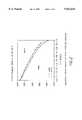
- FIG. 1is a diagram of the etch depth as a function of the etching time in HF/H 2 O vapors.
- FIG. 2is a liquid/vapor phase diagram of HAc/H 2 O mixtures.
- FIG. 3is a diagram of the etch depth as a function of the etching time in HF/HAc vapors.
- FIG. 4is the interpretation of empirical model graphs.
- the HF vapor etchingis performed with a mixture of HF and H 2 O vapors.
- HF vaporcan be generated by feeding a carrier gas like N 2 through a container with a mixture of liquid HF/H 2 O.
- a bottle with anhydrous HFcan be used as the source for HF vapor.
- anhydrous HF alonehardly etches SiO 2 at room temperature.
- the presence of H 2 Ois therefore preferred to initiate the reaction according to the overall equation:
- the processcan be performed in the static mode and in the dynamic mode.
- the reactorIn the static mode, the reactor is filled with a process gas up to a certain pressure and then the reactor is isolated for some time. Subsequently, the reactor is evacuated and the etch cycle can be repeated for a number of times. In the dynamic mode, a continuous flow of process gas is fed into the reactor which is maintained at a constant pressure.
- the processis inflicted with an incubation time: under the chosen conditions, the first 10 minutes very limited etching occurs, see FIG. 1.
- the incubation timeis found to depend on the pretreatment of the wafers.
- An RCA-cleaning just prior to the HF vapor etchingreduces the inhibition time. This is related to the concentration of adsorbed H 2 O molecules on the oxide surface.
- the onset of the etching processcritically depends on the amount of molecules adsorbed on the silicon oxide surface. Water adsorption on the silicon oxide surface in its turn is dependent on the number of OH centers already present on the surface and in this way is dependent on the quality of the oxide.
- Uniform etchingis another important criterion that determines the usefulness of the process.
- the uniformity within the wafer and from wafer to wafer for a process using a batch of 6 wafersis represented in table 1.
- column 5 of said table 1the standard deviation within the wafer is shown. As can be seen from these values, the standard deviation within the wafer is not very good (32%). Also there is quite a standard deviation from the wafer to wafer on the mean etch depth. In the presented case it is 27%. All these values show that the vapor HF/H 2 O mixture does etch the SiO 2 but has not a good performance regarding reproducibility, within wafer uniformity and wafer to wafer uniformity.
- the present inventionis based on the consideration that the good reproducibility of the etching operation may be obtained by use in the gas phase of the new mixtures of the present invention comprising carboxylic acid mixed with HF and possibly in admixture with H 2 O.
- Anhydrous HFhardly etches silicon oxide at room temperature.
- a catalystis necessary to start the reaction.
- H 2 Ocan fulfil this role, the adsorption of H 2 O on the silicon oxide surface is dependent on the number of OH centers already present and in this way on the quality of the oxide.
- the adsorption of organic moleculesshows a strongly reduced sensitivity for the amount of OH groups on the surface.
- the maximum density of adsorbed moleculesstrongly depends on the type of molecule. In table 2, the surface area occupied per adsorbed molecule is given for a number of different molecules. Obviously, acetic acid occupies the smallest surface area.
- acetic acidis a good choice regarding melting point (17° C.), boiling point (118° C.) and the shape of the carboxylic acid/H 2 O liquid/vapor phase diagram.
- other carboxylic acids having similar propertiesmight be equally good or better choices.
- the reactioninvolves the formation of SiF 4 and H 2 O which are both gases at the used pressures:
- the acetic acidonly serves as catalyst
- the etching of SiO 2 by HFgenerates water on the wafer surface.
- This wateris, together with the acetic acid and the HF, assumed to be present in the form of a thin liquid film on the surface of the wafer and must be transported away from the wafer surface by evaporation.
- the acetic acid/H 2 O phase diagram for liquid/vapor equilibriais determining.
- This phase diagramis shown in FIG. 2.
- the vapor and liquid curvesare close together. This means that the composition of the vapor leaving the surface is close to the composition of the liquid on the surface.
- the shape of the curveimplies that the vapor is even somewhat more water rich than the liquid. Consequently, the water generated on the surface can easily be transported away.
- the liquid and vapor curvesare far apart resulting in a large difference between composition of the liquid and the vapor.
- the shape of the curvesis such that the vapor is substantially less water rich than the liquid. Hence the water is not easily removed from the surface, giving rise to a strong increase in surface water concentration in the course of the etching process. This results in a fundamental controllability problem of the etching process which is not present with carboxylic acids and especially acetic acid.
- FIG. 3illustrates as an example the etching behavior of a mixture in accordance with the invention.
- the etch depth as a function of timeis shown when SiO 2 is etched in an HF/acetic acid gas phase mixture.
- the reproducibilityis very good since the time evolution is very smooth. It must be noted that the processes which were run to generate this graph were run over different days and still the measured etch depths fall on a smooth curve showing the high degree of reproducibility.
- Acetic acidappears to have a similar catalytic effect on the HF etch process as H 2 O because substantial etch rates are achieved.
- etch timeFor the static etch mode, a perfectly proportional relation between etch time and etch depth is found until for large times the curve flattens out because of depletion effects. No incubation time can be observed.
- the HF/acetic acid parameter spacewas investigated according to the matrix given in table 4. Modelling the results gave the graphs as presented in FIG. 4. The influence of acetic acid on the etching process is substantial.
- the acetic acid partial pressureprovides a means to reduce the variation in etch depth over the wafer and over the batch and improves the controllability of the process.
- Densification of the TEOS oxide after depositionsubstantially reduces the etch rate but the etch rate still remains higher than that of thermal oxide.
- the selectivityis close to 1 to allow a controlled removal of different types of oxides that can simultaneously be present.
- the performance of the HF/acetic acid mixtureis in this respect approximately equivalent to the liquid mixture.
- Tests for particle contaminationshowed in the HF/acetic acid vapor etch process an average increase of 46 light point defects (0.12 ⁇ m Latex Sphere Equivalent) per 125 mm wafer, which is very low.
- the method according to the subject inventionwas realized in a reaction chamber equipped with three inlets: one for anhydrous HF, one for acetic acid and one for a dry N 2 purge.
- the gas lines for HF and acetic acidare heated to approximately 50° C.
- a metal bottle with anhydrous HF at room temperatureis used as source for the HF vapor.
- Acetic acidis supplied from a quartz bottle which is maintained at 45° C.
- the flows of the vaporsare controlled by Mass Flow Controllers.
- the inlet lineswere combined at a distance of about 50 cm above the reactor.
- the reactor and associated equipment according to the inventionwas made from materials chemically resistant to the reactive HF/carboxylic acid/water mixtures.
- the reactor and some other partswere made of stainless steel and coated with Halar®.
- the wafer boat and the part of the gas lines that is exposed to the vapor mixtureswere made of Monel.
- the gas lines that are exposed to only one of the individual vaporsis made of electropolished stainless steel. A proper choice is of great importance as the entire purpose of the etch is defeated if the removal of the native oxide would lead to an excessive generation of particles from either the reactor walls, the wafer support structure, the gas feed lines, etc.
- the reactoris loaded with a batch comprising 4-25 silicon wafers, being kept at ambient temperature. Subsequently, the reactor chamber loaded with wafers is evacuated. After evacuation, the valve to the pump is closed. After this the inlet of HAc vapor is opened and HAc vapor is injected into the reactor up to a pressure of 600 Pa. Then the HAc inlet is closed. After this, the HF inlet is opened, HF vapor is injected into the reactor up to a total pressure of 900 Pa (partial HF pressure is 300 Pa) and the HF inlet is closed. The wafers are subsequently kept isolated in the system for some time, in this case 200 seconds. After said time interval has elapsed, the pump valve is opened and the process gases are pumped away. Then the reactor is purged with dry N 2 to atmospheric pressure.
Landscapes
- Engineering & Computer Science (AREA)
- Computer Hardware Design (AREA)
- Physics & Mathematics (AREA)
- Condensed Matter Physics & Semiconductors (AREA)
- General Physics & Mathematics (AREA)
- Manufacturing & Machinery (AREA)
- Chemical & Material Sciences (AREA)
- Microelectronics & Electronic Packaging (AREA)
- Power Engineering (AREA)
- General Chemical & Material Sciences (AREA)
- Inorganic Chemistry (AREA)
- Chemical Kinetics & Catalysis (AREA)
- Drying Of Semiconductors (AREA)
Abstract
Description
(H.sub.2 O)SiO.sub.2 +4HF→SiF.sub.4 +2H.sub.2 O
(HAc)SiO.sub.2 +HF→SiF.sub.4 +2H.sub.2 O
TABLE 1______________________________________Etching results in HF/H.sub.2 O vapor Minimal etch Maximal etch Mean etch depth StandardWafer depth (Å) depth (Å) (Å) deviation______________________________________1 38 150 85 382 26 106 50 323 38 104 61 264 38 113 65 265 18 97 43 376 22 89 45 34______________________________________
TABLE 2______________________________________Surface area occupied by different molecules adsorbed onsilicon dioxide Surface area/moleculeMolecule Formula (Å**2)______________________________________Acetic Acid CH.sub.3 COOH 9.1Water H.sub.2 O 12.5Nitrogen N.sub.2 16.4Methanol CH.sub.3 OH 18.0Ethanol C.sub.2 H.sub.5 OH 18.0n-Propanol C.sub.3 H.sub.7 OH 21.3Hexene C.sub.6 H.sub.6 55.0______________________________________
TABLE 3______________________________________Etching results in HF/HAc vapor Minimal etch Maximal etch Mean etch depth StandardWafer depth (Å) depth (Å) (Å) deviation______________________________________1 71 97 84 5.82 75 100 89 7.73 72 97 86 6.24 71 91 82 4.6______________________________________
TABLE 4______________________________________Experimental matrix to investigate the HAc/HF parameter space w-wP.sub.HF P.sub.HAc Etch depth p-p deviation deviation contact anglePa Pa Å % % °______________________________________200 200 83.5 15.9 2.4 59.8400 200 200.5 13.4 7.6 62.0200 800 181.6 7.7 4.9 61.1400 800 395.3 6.7 1.6 62.9300 500 216.1 11.6 1.7 58.1300 200 155.9 14.5 4.4 58.9200 500 148.1 12.6 1.4 58.8300 800 288.7 10.2 2.6 62.8400 500 299.7 12.1 2.9 62.5______________________________________
TABLE 5______________________________________Etch rate selectivity for TEOS oxide/thermal oxideMixture As-deposited Half densified Densified______________________________________liquid, 8.5 5.0 1.40.5 vol % HF in H2Ovapor, 12.0 4.1 1.4300 Pa HF,600 Pa HAcAs-deposited TEOS oxide 725 ° C., low pressureHalf densified TEOS oxide 850° C. for 0.5 h in N.sub.2Densified TEOS oxide 1050° C. for 1 h in N.sub.2______________________________________
Claims (18)
Applications Claiming Priority (4)
| Application Number | Priority Date | Filing Date | Title |
|---|---|---|---|
| EP93870080 | 1993-05-13 | ||
| EP93870080 | 1993-05-13 | ||
| PCT/EP1994/001534WO1994027315A1 (en) | 1993-05-13 | 1994-05-10 | Method for semiconductor processing using mixtures of hf and carboxylic acid |
| WOPCT/EP94/01534 | 1994-05-10 |
Related Parent Applications (1)
| Application Number | Title | Priority Date | Filing Date |
|---|---|---|---|
| US08557065Continuation | 1995-11-13 |
Publications (1)
| Publication Number | Publication Date |
|---|---|
| US5922624Atrue US5922624A (en) | 1999-07-13 |
Family
ID=26070104
Family Applications (1)
| Application Number | Title | Priority Date | Filing Date |
|---|---|---|---|
| US08/772,338Expired - LifetimeUS5922624A (en) | 1993-05-13 | 1996-12-23 | Method for semiconductor processing using mixtures of HF and carboxylic acid |
Country Status (1)
| Country | Link |
|---|---|
| US (1) | US5922624A (en) |
Cited By (28)
| Publication number | Priority date | Publication date | Assignee | Title |
|---|---|---|---|---|
| US6140247A (en)* | 1995-03-10 | 2000-10-31 | Kabushiki Kaisha Toshiba | Semiconductor device manufacturing method |
| US20020157686A1 (en)* | 1997-05-09 | 2002-10-31 | Semitool, Inc. | Process and apparatus for treating a workpiece such as a semiconductor wafer |
| US20030188765A1 (en)* | 2002-04-03 | 2003-10-09 | Christenson Kurt Karl | Transition flow treatment process and apparatus |
| US20040020513A1 (en)* | 1997-05-09 | 2004-02-05 | Semitool, Inc. | Methods of thinning a silicon wafer using HF and ozone |
| US20040221877A1 (en)* | 1997-05-09 | 2004-11-11 | Semitool, Inc. | Process and apparatus for treating a workpiece with gases |
| US20050034745A1 (en)* | 1997-05-09 | 2005-02-17 | Semitool, Inc. | Processing a workpiece with ozone and a halogenated additive |
| US20050053964A1 (en)* | 2000-11-15 | 2005-03-10 | Minerva Biotechnologies Corporation | Oligonucleotide identifiers |
| US20050072446A1 (en)* | 1997-05-09 | 2005-04-07 | Bergman Eric J. | Process and apparatus for treating a workpiece |
| US20050133067A1 (en)* | 1997-05-09 | 2005-06-23 | Bergman Eric J. | Processing a workpiece using water, a base, and ozone |
| US20050189575A1 (en)* | 2004-02-27 | 2005-09-01 | Kevin Torek | Semiconductor fabrication that includes surface tension control |
| US20050215063A1 (en)* | 1997-05-09 | 2005-09-29 | Bergman Eric J | System and methods for etching a silicon wafer using HF and ozone |
| US20050236363A1 (en)* | 1997-05-09 | 2005-10-27 | Bergman Eric J | System and methods for polishing a wafer |
| US20060040467A1 (en)* | 2004-08-20 | 2006-02-23 | Dolechek Kert L | Process and apparatus for thinning a semiconductor workpiece |
| US20060040111A1 (en)* | 2004-08-20 | 2006-02-23 | Dolechek Kert L | Process chamber and system for thinning a semiconductor workpiece |
| US20060046499A1 (en)* | 2004-08-20 | 2006-03-02 | Dolechek Kert L | Apparatus for use in thinning a semiconductor workpiece |
| US20060118515A1 (en)* | 2004-08-20 | 2006-06-08 | Semitool, Inc. | Process For Thinning A Semiconductor Workpiece |
| US20070240826A1 (en)* | 2006-04-18 | 2007-10-18 | Taiwan Semiconductor Manufacturing Co., Ltd. | Gas supply device and apparatus for gas etching or cleaning substrates |
| US7354649B2 (en) | 2004-08-20 | 2008-04-08 | Semitool, Inc. | Semiconductor workpiece |
| US20100252070A1 (en)* | 2007-12-07 | 2010-10-07 | Sumco Corporation | Method for cleaning silicon wafer and apparatus for cleaning the silicon wafer |
| US20160056054A1 (en)* | 2013-05-02 | 2016-02-25 | Fujifilm Corporation | Etching method, etching liquid and etching liquid kit to be used in said method, and semiconductor substrate product manufacturing method |
| EP3041034A1 (en)* | 2015-01-05 | 2016-07-06 | LAM Research Corporation | Isotropic atomic layer etch for silicon and germanium oxides |
| US20190244828A1 (en)* | 2016-10-08 | 2019-08-08 | Beijing Naura Microelectronics Equipment Co., Ltd. | Method for removing silicon oxide and integrated circuit manufacturing process |
| US10679868B2 (en) | 2015-01-06 | 2020-06-09 | Lam Research Corporation | Isotropic atomic layer etch for silicon oxides using no activation |
| US11024512B1 (en) | 2020-03-06 | 2021-06-01 | International Business Machines Corporation | Selective etch formulation for silicon oxide |
| US11289340B2 (en) | 2017-11-14 | 2022-03-29 | Central Glass Company, Limited | Dry etching method |
| US11380556B2 (en) | 2018-05-25 | 2022-07-05 | Lam Research Corporation | Thermal atomic layer etch with rapid temperature cycling |
| US11637022B2 (en) | 2018-07-09 | 2023-04-25 | Lam Research Corporation | Electron excitation atomic layer etch |
| US12280091B2 (en) | 2021-02-03 | 2025-04-22 | Lam Research Corporation | Etch selectivity control in atomic layer etching |
Citations (8)
| Publication number | Priority date | Publication date | Assignee | Title |
|---|---|---|---|---|
| DE1302175B (en)* | 1963-09-25 | 1970-07-23 | ||
| US4749440A (en)* | 1985-08-28 | 1988-06-07 | Fsi Corporation | Gaseous process and apparatus for removing films from substrates |
| EP0272799A1 (en)* | 1986-11-26 | 1988-06-29 | Quick Technologies Ltd. | Ablative etch resistant coating for laser personalization of integrated circuits |
| US5022961A (en)* | 1989-07-26 | 1991-06-11 | Dainippon Screen Mfg. Co., Ltd. | Method for removing a film on a silicon layer surface |
| EP0488198A1 (en)* | 1990-11-28 | 1992-06-03 | Dainippon Screen Mfg. Co., Ltd. | Gaseous process for selectively removing silicon nitride film |
| US5167761A (en)* | 1989-11-03 | 1992-12-01 | Asm International N.V. | Method for halide etching in the presence of water of semi-conductor substrates |
| EP0536752A2 (en)* | 1991-10-11 | 1993-04-14 | Air Products And Chemicals, Inc. | Process for cleaning integrated circuits during the fabrication |
| EP0536747A2 (en)* | 1991-10-11 | 1993-04-14 | Air Products And Chemicals, Inc. | Halogenated carboxylic acid cleaning agents for fabricating integrated circuits and a process for using the same |
- 1996
- 1996-12-23USUS08/772,338patent/US5922624A/ennot_activeExpired - Lifetime
Patent Citations (10)
| Publication number | Priority date | Publication date | Assignee | Title |
|---|---|---|---|---|
| DE1302175B (en)* | 1963-09-25 | 1970-07-23 | ||
| US4749440A (en)* | 1985-08-28 | 1988-06-07 | Fsi Corporation | Gaseous process and apparatus for removing films from substrates |
| EP0272799A1 (en)* | 1986-11-26 | 1988-06-29 | Quick Technologies Ltd. | Ablative etch resistant coating for laser personalization of integrated circuits |
| US5022961A (en)* | 1989-07-26 | 1991-06-11 | Dainippon Screen Mfg. Co., Ltd. | Method for removing a film on a silicon layer surface |
| US5022961B1 (en)* | 1989-07-26 | 1997-05-27 | Dainippon Screen Mfg | Method for removing a film on a silicon layer surface |
| US5167761A (en)* | 1989-11-03 | 1992-12-01 | Asm International N.V. | Method for halide etching in the presence of water of semi-conductor substrates |
| EP0488198A1 (en)* | 1990-11-28 | 1992-06-03 | Dainippon Screen Mfg. Co., Ltd. | Gaseous process for selectively removing silicon nitride film |
| EP0536752A2 (en)* | 1991-10-11 | 1993-04-14 | Air Products And Chemicals, Inc. | Process for cleaning integrated circuits during the fabrication |
| EP0536747A2 (en)* | 1991-10-11 | 1993-04-14 | Air Products And Chemicals, Inc. | Halogenated carboxylic acid cleaning agents for fabricating integrated circuits and a process for using the same |
| US5213622A (en)* | 1991-10-11 | 1993-05-25 | Air Products And Chemicals, Inc. | Cleaning agents for fabricating integrated circuits and a process for using the same |
Non-Patent Citations (10)
| Title |
|---|
| Iler et al., "The Colloid Chemistry of Silica and Silicates," Cornell University Press, Ithaca, NY (1955), Contents and pp. 252-255. |
| Iler et al., The Colloid Chemistry of Silica and Silicates, Cornell University Press, Ithaca, NY (1955), Contents and pp. 252 255.* |
| Kern, W., et al. (1970) Cleaning solutions based on hydrogen peroxide for use in silicon semiconductor technology. RCA Review 187 206.* |
| Kern, W., et al. (1970) Cleaning solutions based on hydrogen peroxide for use in silicon semiconductor technology. RCA Review 187-206. |
| Robbins et al., "Chemical Etching of Silicon," J. Electrochem. Soc. 107:108-111 (1960). |
| Robbins et al., Chemical Etching of Silicon, J. Electrochem. Soc. 107:108 111 (1960).* |
| Winters et al., "Gaseous Products from the Reaction of XeF2 with Silicon," J. Appl. Phys. 54:1218-1223 (1983). |
| Winters et al., Gaseous Products from the Reaction of XeF 2 with Silicon, J. Appl. Phys. 54:1218 1223 (1983).* |
| Wong, M., et al. (1991) Characterization of wafer cleaning and oxide etching using vapor phase hydrogen fluoride. Journal of the Electorchemical Society 138(6):1799 1802.* |
| Wong, M., et al. (1991) Characterization of wafer cleaning and oxide etching using vapor-phase hydrogen fluoride. Journal of the Electorchemical Society 138(6):1799-1802. |
Cited By (46)
| Publication number | Priority date | Publication date | Assignee | Title |
|---|---|---|---|---|
| US6140247A (en)* | 1995-03-10 | 2000-10-31 | Kabushiki Kaisha Toshiba | Semiconductor device manufacturing method |
| US20050215063A1 (en)* | 1997-05-09 | 2005-09-29 | Bergman Eric J | System and methods for etching a silicon wafer using HF and ozone |
| US20050133067A1 (en)* | 1997-05-09 | 2005-06-23 | Bergman Eric J. | Processing a workpiece using water, a base, and ozone |
| US20040020513A1 (en)* | 1997-05-09 | 2004-02-05 | Semitool, Inc. | Methods of thinning a silicon wafer using HF and ozone |
| US20040103919A1 (en)* | 1997-05-09 | 2004-06-03 | Michael Kenny | Single wafer cleaning with ozone |
| US20040221877A1 (en)* | 1997-05-09 | 2004-11-11 | Semitool, Inc. | Process and apparatus for treating a workpiece with gases |
| US20050034745A1 (en)* | 1997-05-09 | 2005-02-17 | Semitool, Inc. | Processing a workpiece with ozone and a halogenated additive |
| US7163588B2 (en) | 1997-05-09 | 2007-01-16 | Semitool, Inc. | Processing a workpiece using water, a base, and ozone |
| US7378355B2 (en) | 1997-05-09 | 2008-05-27 | Semitool, Inc. | System and methods for polishing a wafer |
| US7404863B2 (en)* | 1997-05-09 | 2008-07-29 | Semitool, Inc. | Methods of thinning a silicon wafer using HF and ozone |
| US20020157686A1 (en)* | 1997-05-09 | 2002-10-31 | Semitool, Inc. | Process and apparatus for treating a workpiece such as a semiconductor wafer |
| US20050072446A1 (en)* | 1997-05-09 | 2005-04-07 | Bergman Eric J. | Process and apparatus for treating a workpiece |
| US7416611B2 (en) | 1997-05-09 | 2008-08-26 | Semitool, Inc. | Process and apparatus for treating a workpiece with gases |
| US20050236363A1 (en)* | 1997-05-09 | 2005-10-27 | Bergman Eric J | System and methods for polishing a wafer |
| US20050053964A1 (en)* | 2000-11-15 | 2005-03-10 | Minerva Biotechnologies Corporation | Oligonucleotide identifiers |
| US7156927B2 (en) | 2002-04-03 | 2007-01-02 | Fsi International, Inc. | Transition flow treatment process and apparatus |
| US20030188765A1 (en)* | 2002-04-03 | 2003-10-09 | Christenson Kurt Karl | Transition flow treatment process and apparatus |
| WO2005016563A1 (en)* | 2003-07-30 | 2005-02-24 | Semitool, Inc. | Methods of thinning a silicon wafer using hf and ozone |
| US20050189575A1 (en)* | 2004-02-27 | 2005-09-01 | Kevin Torek | Semiconductor fabrication that includes surface tension control |
| US20060007764A1 (en)* | 2004-02-27 | 2006-01-12 | Micron Technology, Inc. | Semiconductor fabrication that includes surface tension control |
| US20060008926A1 (en)* | 2004-02-27 | 2006-01-12 | Micron Technology, Inc. | Semiconductor fabrication that includes surface tension control |
| US20070173013A1 (en)* | 2004-02-27 | 2007-07-26 | Micron Technology, Inc. | Semiconductor fabrication that includes surface tension control |
| US7214978B2 (en)* | 2004-02-27 | 2007-05-08 | Micron Technology, Inc. | Semiconductor fabrication that includes surface tension control |
| US7193295B2 (en) | 2004-08-20 | 2007-03-20 | Semitool, Inc. | Process and apparatus for thinning a semiconductor workpiece |
| US20060040111A1 (en)* | 2004-08-20 | 2006-02-23 | Dolechek Kert L | Process chamber and system for thinning a semiconductor workpiece |
| US20060046499A1 (en)* | 2004-08-20 | 2006-03-02 | Dolechek Kert L | Apparatus for use in thinning a semiconductor workpiece |
| US7288489B2 (en) | 2004-08-20 | 2007-10-30 | Semitool, Inc. | Process for thinning a semiconductor workpiece |
| US7354649B2 (en) | 2004-08-20 | 2008-04-08 | Semitool, Inc. | Semiconductor workpiece |
| US20060040467A1 (en)* | 2004-08-20 | 2006-02-23 | Dolechek Kert L | Process and apparatus for thinning a semiconductor workpiece |
| US20060203419A1 (en)* | 2004-08-20 | 2006-09-14 | Semitool, Inc. | Process and apparatus for thinning a semiconductor workpiece |
| US20060118515A1 (en)* | 2004-08-20 | 2006-06-08 | Semitool, Inc. | Process For Thinning A Semiconductor Workpiece |
| US7625821B2 (en) | 2004-08-20 | 2009-12-01 | Semitool, Inc. | Process and apparatus for thinning a semiconductor workpiece |
| US20070240826A1 (en)* | 2006-04-18 | 2007-10-18 | Taiwan Semiconductor Manufacturing Co., Ltd. | Gas supply device and apparatus for gas etching or cleaning substrates |
| US20100252070A1 (en)* | 2007-12-07 | 2010-10-07 | Sumco Corporation | Method for cleaning silicon wafer and apparatus for cleaning the silicon wafer |
| US7955440B2 (en)* | 2007-12-07 | 2011-06-07 | Sumco Corporation | Method for cleaning silicon wafer and apparatus for cleaning the silicon wafer |
| US20160056054A1 (en)* | 2013-05-02 | 2016-02-25 | Fujifilm Corporation | Etching method, etching liquid and etching liquid kit to be used in said method, and semiconductor substrate product manufacturing method |
| EP3041034A1 (en)* | 2015-01-05 | 2016-07-06 | LAM Research Corporation | Isotropic atomic layer etch for silicon and germanium oxides |
| US10679868B2 (en) | 2015-01-06 | 2020-06-09 | Lam Research Corporation | Isotropic atomic layer etch for silicon oxides using no activation |
| US20190244828A1 (en)* | 2016-10-08 | 2019-08-08 | Beijing Naura Microelectronics Equipment Co., Ltd. | Method for removing silicon oxide and integrated circuit manufacturing process |
| US10937661B2 (en)* | 2016-10-08 | 2021-03-02 | Beijing Naura Microelectronics Equipment Co., Ltd. | Method for removing silicon oxide and integrated circuit manufacturing process |
| US11289340B2 (en) | 2017-11-14 | 2022-03-29 | Central Glass Company, Limited | Dry etching method |
| US12387940B2 (en) | 2017-11-14 | 2025-08-12 | Central Glass Company, Limited | Dry etching method |
| US11380556B2 (en) | 2018-05-25 | 2022-07-05 | Lam Research Corporation | Thermal atomic layer etch with rapid temperature cycling |
| US11637022B2 (en) | 2018-07-09 | 2023-04-25 | Lam Research Corporation | Electron excitation atomic layer etch |
| US11024512B1 (en) | 2020-03-06 | 2021-06-01 | International Business Machines Corporation | Selective etch formulation for silicon oxide |
| US12280091B2 (en) | 2021-02-03 | 2025-04-22 | Lam Research Corporation | Etch selectivity control in atomic layer etching |
Similar Documents
| Publication | Publication Date | Title |
|---|---|---|
| US5922624A (en) | Method for semiconductor processing using mixtures of HF and carboxylic acid | |
| EP0698282B1 (en) | Method for etching silicon oxide layers using mixtures of HF and carboxylic acid | |
| EP0500670B1 (en) | Method for halide etching in the presence of water of semi-conductor substrates | |
| US5620559A (en) | Hydrogen radical processing | |
| EP0235256B1 (en) | Gaseous process and apparatus for removing films from substrates | |
| KR100257302B1 (en) | Film Formation Method | |
| US5294568A (en) | Method of selective etching native oxide | |
| US4749440A (en) | Gaseous process and apparatus for removing films from substrates | |
| US5571375A (en) | Method of removing native oxide film from a contact hole on silicon wafer | |
| US6492283B2 (en) | Method of forming ultrathin oxide layer | |
| US20060177987A1 (en) | Methods for forming thin oxide layers on semiconductor wafers | |
| JPH05326480A (en) | Surface treatment apparatus for semiconductor substrate and control method therefor | |
| US20050215063A1 (en) | System and methods for etching a silicon wafer using HF and ozone | |
| JP3101975B2 (en) | Gas phase removal of SiO2 / metal from silicon | |
| US5567332A (en) | Micro-machine manufacturing process | |
| KR100232664B1 (en) | Method and appartus for manufacturing a semiconductor device | |
| US5922219A (en) | UV/halogen treatment for dry oxide etching | |
| US5023206A (en) | Semiconductor device with adjacent non-oxide layers and the fabrication thereof | |
| KR20030083730A (en) | Cleaning method for substrate treatment device and substrate treatment device | |
| JP2632293B2 (en) | Selective removal method of silicon native oxide film | |
| JPH03204932A (en) | Removal of coating film on silicon layer and selective removal of silicon natural oxide film | |
| JPH09102490A (en) | Semiconductor device manufacturing method and semiconductor manufacturing apparatus | |
| JP3401585B2 (en) | Substrate cleaning method | |
| US20070240826A1 (en) | Gas supply device and apparatus for gas etching or cleaning substrates | |
| JP2598524B2 (en) | Dry etching method |
Legal Events
| Date | Code | Title | Description |
|---|---|---|---|
| AS | Assignment | Owner name:INTERUNIVERSITAIR MICRO-ELEKTRONICA CENTRUM (IMEC Free format text:ASSIGNMENT OF ASSIGNORS INTEREST;ASSIGNOR:HEYNS, MARK;REEL/FRAME:008377/0293 Effective date:19961125 Owner name:ADVANCED SEMICONDUCTOR MATERIALS NAAMLOZE VENNOOTS Free format text:ASSIGNMENT OF ASSIGNORS INTEREST;ASSIGNORS:HENDRIKS, MENSO;DE BLANK, RENE;REEL/FRAME:008377/0316 Effective date:19961125 | |
| AS | Assignment | Owner name:INTERUNIVERSITAIRE MICROELEKTRONICA CENTRUM (IMEC Free format text:ASSIGNMENT OF ASSIGNORS INTEREST;ASSIGNOR:VERHAVERBEKE, STEVEN;REEL/FRAME:009567/0361 Effective date:19980921 | |
| STCF | Information on status: patent grant | Free format text:PATENTED CASE | |
| CC | Certificate of correction | ||
| FPAY | Fee payment | Year of fee payment:4 | |
| REMI | Maintenance fee reminder mailed | ||
| FEPP | Fee payment procedure | Free format text:PAYOR NUMBER ASSIGNED (ORIGINAL EVENT CODE: ASPN); ENTITY STATUS OF PATENT OWNER: LARGE ENTITY | |
| FPAY | Fee payment | Year of fee payment:8 | |
| FEPP | Fee payment procedure | Free format text:PAYOR NUMBER ASSIGNED (ORIGINAL EVENT CODE: ASPN); ENTITY STATUS OF PATENT OWNER: LARGE ENTITY Free format text:PAYER NUMBER DE-ASSIGNED (ORIGINAL EVENT CODE: RMPN); ENTITY STATUS OF PATENT OWNER: LARGE ENTITY | |
| FPAY | Fee payment | Year of fee payment:12 |