US5920513A - Partial replacement of partially defective memory devices - Google Patents
Partial replacement of partially defective memory devicesDownload PDFInfo
- Publication number
- US5920513A US5920513AUS08/916,846US91684697AUS5920513AUS 5920513 AUS5920513 AUS 5920513AUS 91684697 AUS91684697 AUS 91684697AUS 5920513 AUS5920513 AUS 5920513A
- Authority
- US
- United States
- Prior art keywords
- memory
- coupled
- memory device
- link
- data line
- Prior art date
- Legal status (The legal status is an assumption and is not a legal conclusion. Google has not performed a legal analysis and makes no representation as to the accuracy of the status listed.)
- Expired - Lifetime
Links
Images


Classifications
- G—PHYSICS
- G11—INFORMATION STORAGE
- G11C—STATIC STORES
- G11C29/00—Checking stores for correct operation ; Subsequent repair; Testing stores during standby or offline operation
- G11C29/70—Masking faults in memories by using spares or by reconfiguring
- G11C29/88—Masking faults in memories by using spares or by reconfiguring with partially good memories
- G—PHYSICS
- G11—INFORMATION STORAGE
- G11C—STATIC STORES
- G11C29/00—Checking stores for correct operation ; Subsequent repair; Testing stores during standby or offline operation
- G11C29/70—Masking faults in memories by using spares or by reconfiguring
- G11C29/78—Masking faults in memories by using spares or by reconfiguring using programmable devices
- G11C29/83—Masking faults in memories by using spares or by reconfiguring using programmable devices with reduced power consumption
- G11C29/832—Masking faults in memories by using spares or by reconfiguring using programmable devices with reduced power consumption with disconnection of faulty elements
Definitions
- the present inventionrelates generally to integrated circuit devices and more particularly to the partial replacement of partially defective integrated circuit memory devices.
- redundant circuit elementsare provided on the devices to reduce the number of scrapped devices. If a primary circuit element of a device is determined to be defective, a redundant circuit element is substituted for the defective primary circuit element. Substantial reductions in scrap are achieved by using redundant circuit elements without substantially increasing the cost of the device.
- the present inventionrelates to the partial replacement of partially defective integrated circuit memory devices.
- a memory devicewhich has one or more links having an initial closed configuration, wherein each link is coupled to a data line coupled to a section of the memory array.
- Each linkis configured to open to permit replacement of just the section of the memory array coupled to the data line to which the link is coupled.
- a multi-chip moduleincludes a plurality of memory devices mounted on a substrate and a plurality of data lines, each coupled to a memory device.
- a normally closed linkis coupled to each data line. If one of the memory devices is partially defective, the appropriate link is opened. This is the link that is coupled to the data line which is coupled to the defective section of the memory device.
- a partially or completely operating memory deviceis coupled to the module at a repair site to replace only the defective section.
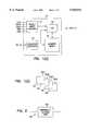
- FIG. 1(a)is a block diagram of a typical memory device in conjunction with which an embodiment of the invention may be implemented;
- FIG. 1(b)is a block diagram showing in more logical detail the memory array of the memory device of FIG. 1(a), according to an embodiment of the invention
- FIG. 2is a block diagram of a normally closed link for a data line of a section of the memory of a memory device, according to one embodiment of the invention
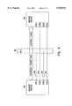
- FIG. 3is a diagram of a multi-chip module according to an embodiment of the invention.
- FIG. 4is a diagram of another multi-chip module according to an embodiment of the invention.
- FIG. 5is a diagram showing in more detail the partially defective device and the repair device shown in FIG. 4;
- FIG. 6is a method illustrating the partial replacement of a partially defective device in one embodiment of the invention.
- Memory device 10includes memory array 12, control circuit 14, input/output buffers 16, and address decoder 18.
- Memory array 12includes a plurality of memory cells organized into rows and columns. The memory cells are accessed in response to an address signal provided on the address lines A0 . . . AN running to address decoder 18, which includes both row and column decoder circuitry.
- Input/output buffers 16are provided for bidirectional communication via the data communications lines DQ1 . . . DQN running out of buffers 16.
- Control circuit 14regulates the memory device operations in response to controls signals including, but not limited to, a Clock (CLK), a Row Access Strobe (RAS*), a Column Access Strobe (CAS*), a Write Enable (WE*), and a Clock Enable (CKE).
- CLKClock
- RAS*Row Access Strobe
- CAS*Column Access Strobe
- WE*Write Enable
- CKEClock Enable
- Memory array 12is shown in more logical detail in FIG. 1(b).
- the memory arrayis divided into planes 20, 22, 24 and 26.
- Each of the planescorresponds to a particular data line (i.e., DQ1, DQ2, DQ3 or DQ4).
- Each of the planesis a separate section of the memory array.
- the separate sectionsare shown as different planes to better illustrate the organization of the memory cells of the array. This does not, however, necessarily correspond to the actual physical construction of the array.
- Each data linecan access only those memory cells within the plane of the array to which it corresponds. Where one or more memory cells within a particular plane or section are defective, the section is said to be defective.
- the present inventionprovides for replacement of only those sections of the memory array of a memory device that are defective with a repair memory device.
- the present inventionis not limited to any particular type of memory device or repair memory device.
- the devicesare dynamic random-access-memories (DRAMs), including those available from Micron Technology, Inc., of Boise, Id., as part numbers MT4LC4M4D42TC2-6TC (for the memory device) and MT4C4D42SC2-6TRA (for the repair device).
- DRAMsdynamic random-access-memories
- the devicesare static random-access-memories (SRAMs), flash memories, synchronous dynamic random-access-memories (SDRAMs), extended-data-out random-access-memories (EDO RAMs), and burst-extended-data-out random-access-memories (BEDO RAMs), as those skilled in the art will appreciate.
- SRAMsstatic random-access-memories
- SDRAMssynchronous dynamic random-access-memories
- EEO RAMsextended-data-out random-access-memories
- BEDO RAMsburst-extended-data-out random-access-memories
- FIG. 2A block diagram of a normally closed link for a data line of a section of the memory array of a memory device is shown in FIG. 2.
- Data line 28is representative of each of the data lines shown in FIG. 1(a) and FIG. 1(b).
- Data line 28has inserted in series therein normally closed link 30.
- Link 30is normally closed in that it has an initial closed configuration such that it permits electrical current to travel through data line 28.
- Link 30is configured to open such that when link 30 is open (that is, link 30 is in an opened configuration), no electrical current can travel through data line 28. Therefore, the section of the memory array to which a data line is coupled may be disabled by opening the normally closed link for the data line. This opens the data line and does not permit electrical current to travel to or from that section of the array.
- the linkis a standard polysilicon fuse or resistor link.
- the fusecomprises a polysilicon conductor approximately 1 ⁇ thick, which is fabricated such that in its normal state there is a complete electrical path through the fuse.
- a high power laseris used to open the electrical path by evaporating a portion of the polysilicon.
- a burst of high currentis asserted to the data line to open the path by blowing the fuse.
- Multi-chip module 32may be a single in-line memory module (SIMM), or any other type of multi-chip module.
- Multi-chip moduleincludes substrate 34, with bus 36 and memory devices 38, 40, 42, 44, 46, 48, 50 and 52 mounted thereon.
- Bus 36permits coupling of module 32 to a computer or other device receptive to the module.
- Substrate 34also includes space for a maximum of two repair devices to be mounted thereon. These are shown as repair sites 54 and 56.
- the control linese.g., CLK, RAS*, CAS*, WE*, and CKE
- the address linese.g., A0 . . . AN
- the data linese.g., DQ1 . . . DQN
- Each data lineincludes a normally closed link inserted in series therein.
- memory device 38has data lines with normally closed links 58, 60, 62 and 64.
- each of the normally closed linkspermits the individual enablement of a section of the memory array of a memory device. As shown in FIG. 3, none of the links are opened. All the sections of the memory arrays of all the memory devices are enabled.
- FIG. 4is a block diagram of a multi-chip module according to an embodiment of the invention. As compared to FIG. 3, the data lines for all the memory devices except device 38 are not shown for sake of clarity.
- Multi-chip module 32 in FIG. 4has repair device 66 mounted to substrate 34, at the location specified as repair site 54 in FIG. 3. While links 58 and 62 of memory device 38 remain closed in FIG. 4, links 60 and 64 are open, as shown by dotted lines. This means that the sections of the memory array of device 38 to which links 60 and 64 are coupled via data lines cannot receive communications to or from bus 36. They are effectively disabled, even though the remainder of memory device 38 is operable (i.e., the sections of the memory array to which links 58 and 62 are coupled via data lines).
- the control lines (e.g., CLK, RAS*, CAS*, WE*, and CKE) and the address lines (e.g., A0 . . . AN) of repair device 66are each coupled to the corresponding control and address lines of memory device 38 (not shown in FIG. 4). Furthermore, one data line of repair device 66 is coupled to each data line of memory device 38 having a link that is open. Thus, one data line of device 66 couples the data line of device 38 having link 60, and another data line of device 66 couples the data line of device 38 having link 64. Insofar as repair device 66 has other data lines, they are not used (i.e., not connected). The data lines of memory device 38 having links that are open--i.e., the line with link 58 and the line with link 62--do not have a data line of memory device 66 coupled thereto.
- FIG. 5a block diagram illustrating memory device 38 and repair device 66 in more detail is shown.
- the DQ1 pin of device 38has closed link 58; therefore, the DQ1 pin of device 66 remains uncoupled.
- the DQ3 pin of device 38has closed link 62; therefore, the DQ3 pin of device 66 remains uncoupled.
- the DQ2 pin of device 38has opened link 60; therefore, the DQ2 pin of device 66 is coupled to the DQ2 port of bus 36.
- the DQ4 pin of device 38has opened link 64; therefore, the DQ4 pin of device 66 is coupled to the DQ4 port of bus 36. All other pins of the devices are coupled to the bus (not shown in FIG. 5), such that corresponding address and control lines of the devices are coupled to one another.
- repair device 66only replaces those sections of device 38 that are defective.
- the section of the memory array of repair device 66 corresponding to data line DQ2 of device 66replaces the section of the memory array of device 38 corresponding to data line DQ2 of device 38.
- the section of the array of device 66 corresponding to data line DQ4 of device 66replaces the section of the memory array of device 38 corresponding to data line DQ4 of device 38.
- the functionality of data lines DQ2 and DQ4is performed by device 66, while the functionality of data lines DQ1 and DQ3 is performed by device 38.
- both device 38 and repair device 66process the command. If the command corresponds to a section of the memory related to DQ1 or DQ3, device 38 provides the output, since its DQ1 and DQ3 lines are coupled to bus 36, while the DQ1 and DQ3 lines of device 66 are not. Conversely, if the command corresponds to a section of the memory related to DQ2 or DQ4, device 66 provides the output, since its DQ2 and DQ4 lines are coupled to bus 36, while the DQ2 and DQ4 lines of device 38 are not due to links 60 and 64 having been opened.
- repair device 66Because the sections of the memory array of repair device 66 that correspond to data lines DQ1 and DQ3 of repair device 66 are not coupled at all, these sections do not have to be operable for device 66 to successfully partially replace device 38. That is, repair device 66 may itself be a partially defective device. So long as it has two operable sections within the memory array to replace the two defective sections of the memory array of device 38, repair device 66 is adequate. This means that otherwise scrap memory devices may still be used as repair devices in conjunction with the present invention, providing for a great economical advantage.
- step 68a defective section of the memory array of a memory device is identified.
- the present inventionis not limited to any particular manner in which the defective section is identified. However, in one embodiment, a logic one is written to each memory cell within the section, and then the memory cell is read. If at least one memory cell does not return a logic one when read, the section is defective.
- step 70the normally closed link coupled to the data line for that section is opened.
- the linkis opened by exposure to a high power laser (i.e., an external heat source).
- the linkis opened by assertion of a high current to the data line to which the link is coupled in series.
- a repair deviceis connected to the memory device such that just the defective section of the memory device is replaced.
- the pins of the repair device corresponding to the address and control linesare coupled to their counterpart pins of the memory device.
- the data line of an operative section of the memory array of the repair deviceis coupled to the data line of the defective section of the memory array of the memory device.
- the data lines for the other sections of the memory array of the repair deviceare not coupled at all. These sections do not have to be operable.
Landscapes
- For Increasing The Reliability Of Semiconductor Memories (AREA)
- Techniques For Improving Reliability Of Storages (AREA)
Abstract
Description
Claims (4)
Priority Applications (3)
| Application Number | Priority Date | Filing Date | Title |
|---|---|---|---|
| US08/916,846US5920513A (en) | 1997-08-22 | 1997-08-22 | Partial replacement of partially defective memory devices |
| US09/326,211US6009025A (en) | 1997-08-22 | 1999-06-04 | Partial replacement of partially defective memory devices |
| US09/451,406US6208578B1 (en) | 1997-08-22 | 1999-11-30 | Partial replacement of partially defective memory devices |
Applications Claiming Priority (1)
| Application Number | Priority Date | Filing Date | Title |
|---|---|---|---|
| US08/916,846US5920513A (en) | 1997-08-22 | 1997-08-22 | Partial replacement of partially defective memory devices |
Related Child Applications (1)
| Application Number | Title | Priority Date | Filing Date |
|---|---|---|---|
| US09/326,211ContinuationUS6009025A (en) | 1997-08-22 | 1999-06-04 | Partial replacement of partially defective memory devices |
Publications (1)
| Publication Number | Publication Date |
|---|---|
| US5920513Atrue US5920513A (en) | 1999-07-06 |
Family
ID=25437922
Family Applications (3)
| Application Number | Title | Priority Date | Filing Date |
|---|---|---|---|
| US08/916,846Expired - LifetimeUS5920513A (en) | 1997-08-22 | 1997-08-22 | Partial replacement of partially defective memory devices |
| US09/326,211Expired - LifetimeUS6009025A (en) | 1997-08-22 | 1999-06-04 | Partial replacement of partially defective memory devices |
| US09/451,406Expired - LifetimeUS6208578B1 (en) | 1997-08-22 | 1999-11-30 | Partial replacement of partially defective memory devices |
Family Applications After (2)
| Application Number | Title | Priority Date | Filing Date |
|---|---|---|---|
| US09/326,211Expired - LifetimeUS6009025A (en) | 1997-08-22 | 1999-06-04 | Partial replacement of partially defective memory devices |
| US09/451,406Expired - LifetimeUS6208578B1 (en) | 1997-08-22 | 1999-11-30 | Partial replacement of partially defective memory devices |
Country Status (1)
| Country | Link |
|---|---|
| US (3) | US5920513A (en) |
Cited By (9)
| Publication number | Priority date | Publication date | Assignee | Title |
|---|---|---|---|---|
| US6314527B1 (en) | 1998-03-05 | 2001-11-06 | Micron Technology, Inc. | Recovery of useful areas of partially defective synchronous memory components |
| US6332183B1 (en)* | 1998-03-05 | 2001-12-18 | Micron Technology, Inc. | Method for recovery of useful areas of partially defective synchronous memory components |
| US6381708B1 (en) | 1998-04-28 | 2002-04-30 | Micron Technology, Inc. | Method for decoding addresses for a defective memory array |
| US6381707B1 (en) | 1998-04-28 | 2002-04-30 | Micron Technology, Inc. | System for decoding addresses for a defective memory array |
| US6496876B1 (en) | 1998-12-21 | 2002-12-17 | Micron Technology, Inc. | System and method for storing a tag to identify a functional storage location in a memory device |
| US6578157B1 (en) | 2000-03-06 | 2003-06-10 | Micron Technology, Inc. | Method and apparatus for recovery of useful areas of partially defective direct rambus rimm components |
| US20050135180A1 (en)* | 2000-06-30 | 2005-06-23 | Micron Technology, Inc. | Interface command architecture for synchronous flash memory |
| US7269765B1 (en) | 2000-04-13 | 2007-09-11 | Micron Technology, Inc. | Method and apparatus for storing failing part locations in a module |
| US20080016391A1 (en)* | 2004-09-29 | 2008-01-17 | Peter Ossimitz | Semiconductor Memory Component Having A Diverting Circuit |
Families Citing this family (3)
| Publication number | Priority date | Publication date | Assignee | Title |
|---|---|---|---|---|
| US20060182187A1 (en)* | 2005-02-11 | 2006-08-17 | Likovich Robert B Jr | Automatic reconfiguration of an I/O bus to correct for an error bit |
| US20120168531A1 (en) | 2011-01-03 | 2012-07-05 | Global Agricultural Technology And Engineering Llc | Liquid delivery system |
| KR102483476B1 (en)* | 2018-04-03 | 2023-01-03 | 에스케이하이닉스 주식회사 | Semiconductor memory apparatus supporting repair with data I/O terminal as a unit and method of repairing the semiconductor memory apparatus |
Citations (7)
| Publication number | Priority date | Publication date | Assignee | Title |
|---|---|---|---|---|
| US4791319A (en)* | 1986-06-20 | 1988-12-13 | Sharp Kabushiki Kaisha | Semiconductor device with redundancy circuit and means for activating same |
| US5107464A (en)* | 1987-11-02 | 1992-04-21 | Kabushiki Kaisha Toshiba | Semiconductor memory system |
| US5200652A (en)* | 1991-11-13 | 1993-04-06 | Micron Technology, Inc. | Programmable/reprogrammable structure combining both antifuse and fuse elements |
| US5265054A (en)* | 1990-12-14 | 1993-11-23 | Sgs-Thomson Microelectronics, Inc. | Semiconductor memory with precharged redundancy multiplexing |
| US5276834A (en)* | 1990-12-04 | 1994-01-04 | Micron Technology, Inc. | Spare memory arrangement |
| US5703817A (en)* | 1995-11-17 | 1997-12-30 | Kabushiki Kaisha Toshiba | Semiconductor memory device |
| US5706231A (en)* | 1996-06-27 | 1998-01-06 | Mitsubishi Denki Kabushiki Kaisha | Semiconductor memory device having a redundant memory cell |
- 1997
- 1997-08-22USUS08/916,846patent/US5920513A/ennot_activeExpired - Lifetime
- 1999
- 1999-06-04USUS09/326,211patent/US6009025A/ennot_activeExpired - Lifetime
- 1999-11-30USUS09/451,406patent/US6208578B1/ennot_activeExpired - Lifetime
Patent Citations (7)
| Publication number | Priority date | Publication date | Assignee | Title |
|---|---|---|---|---|
| US4791319A (en)* | 1986-06-20 | 1988-12-13 | Sharp Kabushiki Kaisha | Semiconductor device with redundancy circuit and means for activating same |
| US5107464A (en)* | 1987-11-02 | 1992-04-21 | Kabushiki Kaisha Toshiba | Semiconductor memory system |
| US5276834A (en)* | 1990-12-04 | 1994-01-04 | Micron Technology, Inc. | Spare memory arrangement |
| US5265054A (en)* | 1990-12-14 | 1993-11-23 | Sgs-Thomson Microelectronics, Inc. | Semiconductor memory with precharged redundancy multiplexing |
| US5200652A (en)* | 1991-11-13 | 1993-04-06 | Micron Technology, Inc. | Programmable/reprogrammable structure combining both antifuse and fuse elements |
| US5703817A (en)* | 1995-11-17 | 1997-12-30 | Kabushiki Kaisha Toshiba | Semiconductor memory device |
| US5706231A (en)* | 1996-06-27 | 1998-01-06 | Mitsubishi Denki Kabushiki Kaisha | Semiconductor memory device having a redundant memory cell |
Non-Patent Citations (2)
| Title |
|---|
| "Micron Technology, Inc.4 MEG x 4 DRAM catalog pages", 3-33 to 3-48, (1995). |
| Micron Technology, Inc.4 MEG x 4 DRAM catalog pages , 3 33 to 3 48, (1995).* |
Cited By (14)
| Publication number | Priority date | Publication date | Assignee | Title |
|---|---|---|---|---|
| US6314527B1 (en) | 1998-03-05 | 2001-11-06 | Micron Technology, Inc. | Recovery of useful areas of partially defective synchronous memory components |
| US6332183B1 (en)* | 1998-03-05 | 2001-12-18 | Micron Technology, Inc. | Method for recovery of useful areas of partially defective synchronous memory components |
| US6621748B2 (en) | 1998-03-05 | 2003-09-16 | Micron Technology, Inc. | Recovery of useful areas of partially defective synchronous memory components |
| US6381707B1 (en) | 1998-04-28 | 2002-04-30 | Micron Technology, Inc. | System for decoding addresses for a defective memory array |
| US6381708B1 (en) | 1998-04-28 | 2002-04-30 | Micron Technology, Inc. | Method for decoding addresses for a defective memory array |
| US6496876B1 (en) | 1998-12-21 | 2002-12-17 | Micron Technology, Inc. | System and method for storing a tag to identify a functional storage location in a memory device |
| US6578157B1 (en) | 2000-03-06 | 2003-06-10 | Micron Technology, Inc. | Method and apparatus for recovery of useful areas of partially defective direct rambus rimm components |
| US6810492B2 (en) | 2000-03-06 | 2004-10-26 | Micron Technology, Inc. | Apparatus and system for recovery of useful areas of partially defective direct rambus RIMM components |
| US7269765B1 (en) | 2000-04-13 | 2007-09-11 | Micron Technology, Inc. | Method and apparatus for storing failing part locations in a module |
| US20070288805A1 (en)* | 2000-04-13 | 2007-12-13 | Charlton David E | Method and apparatus for storing failing part locations in a module |
| US7890819B2 (en) | 2000-04-13 | 2011-02-15 | Micron Technology, Inc. | Method and apparatus for storing failing part locations in a module |
| US20050135180A1 (en)* | 2000-06-30 | 2005-06-23 | Micron Technology, Inc. | Interface command architecture for synchronous flash memory |
| US20080016391A1 (en)* | 2004-09-29 | 2008-01-17 | Peter Ossimitz | Semiconductor Memory Component Having A Diverting Circuit |
| US8799704B2 (en)* | 2004-09-29 | 2014-08-05 | Infineon Technologies Ag | Semiconductor memory component having a diverting circuit |
Also Published As
| Publication number | Publication date |
|---|---|
| US6009025A (en) | 1999-12-28 |
| US6208578B1 (en) | 2001-03-27 |
Similar Documents
| Publication | Publication Date | Title |
|---|---|---|
| US5747869A (en) | Reduced pitch laser redundancy fuse bank structure | |
| US7577882B2 (en) | Semiconductor integrated circuit including memory macro | |
| JP3848004B2 (en) | Semiconductor memory device and semiconductor memory device mounting system | |
| KR100441817B1 (en) | Circuits and methods for enabling functionality in a memory device module | |
| US6163490A (en) | Semiconductor memory remapping | |
| KR100689011B1 (en) | Semiconductor integrated circuit | |
| US5920513A (en) | Partial replacement of partially defective memory devices | |
| KR20040027450A (en) | A method of self-repairing dynamic random access memory | |
| US6819608B2 (en) | Method of recovering memory module, memory module and volatile memory | |
| EP0881571B1 (en) | Semiconductor memory device with redundancy | |
| JPH01224999A (en) | semiconductor storage device | |
| US6937536B2 (en) | Antifuse option for row repair | |
| US6597054B1 (en) | Reduced pitch laser redundancy fuse bank structure | |
| US6366509B2 (en) | Method and apparatus for repairing defective columns of memory cells | |
| US6608783B2 (en) | Twisted bit-line compensation | |
| US6570794B1 (en) | Twisted bit-line compensation for DRAM having redundancy | |
| JP3253462B2 (en) | Semiconductor storage device | |
| US6185136B1 (en) | Method and apparatus for repairing defective columns of memory cells | |
| KR100228522B1 (en) | Semiconductor memory device | |
| KR100192588B1 (en) | Semiconductor memory device with partial chip | |
| US6831870B2 (en) | Semiconductor memory | |
| JPH04241299A (en) | Defect relief method for semiconductor memory device, defect relief circuit, and semiconductor memory device equipped with the same |
Legal Events
| Date | Code | Title | Description |
|---|---|---|---|
| AS | Assignment | Owner name:MICRON TECHNOLOGY, INC., IDAHO Free format text:ASSIGNMENT OF ASSIGNORS INTEREST;ASSIGNOR:JACOBSON, JOHN O.;REEL/FRAME:008691/0874 Effective date:19970821 | |
| STCF | Information on status: patent grant | Free format text:PATENTED CASE | |
| FEPP | Fee payment procedure | Free format text:PAYOR NUMBER ASSIGNED (ORIGINAL EVENT CODE: ASPN); ENTITY STATUS OF PATENT OWNER: LARGE ENTITY | |
| FPAY | Fee payment | Year of fee payment:4 | |
| FPAY | Fee payment | Year of fee payment:8 | |
| FPAY | Fee payment | Year of fee payment:12 | |
| AS | Assignment | Owner name:U.S. BANK NATIONAL ASSOCIATION, AS COLLATERAL AGENT, CALIFORNIA Free format text:SECURITY INTEREST;ASSIGNOR:MICRON TECHNOLOGY, INC.;REEL/FRAME:038669/0001 Effective date:20160426 Owner name:U.S. BANK NATIONAL ASSOCIATION, AS COLLATERAL AGEN Free format text:SECURITY INTEREST;ASSIGNOR:MICRON TECHNOLOGY, INC.;REEL/FRAME:038669/0001 Effective date:20160426 | |
| AS | Assignment | Owner name:MORGAN STANLEY SENIOR FUNDING, INC., AS COLLATERAL AGENT, MARYLAND Free format text:PATENT SECURITY AGREEMENT;ASSIGNOR:MICRON TECHNOLOGY, INC.;REEL/FRAME:038954/0001 Effective date:20160426 Owner name:MORGAN STANLEY SENIOR FUNDING, INC., AS COLLATERAL Free format text:PATENT SECURITY AGREEMENT;ASSIGNOR:MICRON TECHNOLOGY, INC.;REEL/FRAME:038954/0001 Effective date:20160426 | |
| AS | Assignment | Owner name:U.S. BANK NATIONAL ASSOCIATION, AS COLLATERAL AGENT, CALIFORNIA Free format text:CORRECTIVE ASSIGNMENT TO CORRECT THE REPLACE ERRONEOUSLY FILED PATENT #7358718 WITH THE CORRECT PATENT #7358178 PREVIOUSLY RECORDED ON REEL 038669 FRAME 0001. ASSIGNOR(S) HEREBY CONFIRMS THE SECURITY INTEREST;ASSIGNOR:MICRON TECHNOLOGY, INC.;REEL/FRAME:043079/0001 Effective date:20160426 Owner name:U.S. BANK NATIONAL ASSOCIATION, AS COLLATERAL AGEN Free format text:CORRECTIVE ASSIGNMENT TO CORRECT THE REPLACE ERRONEOUSLY FILED PATENT #7358718 WITH THE CORRECT PATENT #7358178 PREVIOUSLY RECORDED ON REEL 038669 FRAME 0001. ASSIGNOR(S) HEREBY CONFIRMS THE SECURITY INTEREST;ASSIGNOR:MICRON TECHNOLOGY, INC.;REEL/FRAME:043079/0001 Effective date:20160426 | |
| AS | Assignment | Owner name:MICRON TECHNOLOGY, INC., IDAHO Free format text:RELEASE BY SECURED PARTY;ASSIGNOR:U.S. BANK NATIONAL ASSOCIATION, AS COLLATERAL AGENT;REEL/FRAME:047243/0001 Effective date:20180629 | |
| AS | Assignment | Owner name:MICRON TECHNOLOGY, INC., IDAHO Free format text:RELEASE BY SECURED PARTY;ASSIGNOR:MORGAN STANLEY SENIOR FUNDING, INC., AS COLLATERAL AGENT;REEL/FRAME:050937/0001 Effective date:20190731 |