US5920230A - HEMT-HBT cascode distributed amplifier - Google Patents
HEMT-HBT cascode distributed amplifierDownload PDFInfo
- Publication number
- US5920230A US5920230AUS08/955,379US95537997AUS5920230AUS 5920230 AUS5920230 AUS 5920230AUS 95537997 AUS95537997 AUS 95537997AUS 5920230 AUS5920230 AUS 5920230A
- Authority
- US
- United States
- Prior art keywords
- amplifier
- recited
- distributed amplifier
- transmission line
- transistor
- Prior art date
- Legal status (The legal status is an assumption and is not a legal conclusion. Google has not performed a legal analysis and makes no representation as to the accuracy of the status listed.)
- Expired - Lifetime
Links
- 230000005540biological transmissionEffects0.000claimsdescription22
- 230000005669field effectEffects0.000claimsdescription11
- 230000001965increasing effectEffects0.000abstractdescription7
- 230000015556catabolic processEffects0.000description8
- 239000003990capacitorSubstances0.000description6
- 238000000034methodMethods0.000description4
- 238000010586diagramMethods0.000description3
- 230000000694effectsEffects0.000description2
- 230000004044responseEffects0.000description2
- 230000003321amplificationEffects0.000description1
- 230000009286beneficial effectEffects0.000description1
- 230000000593degrading effectEffects0.000description1
- 230000001939inductive effectEffects0.000description1
- 230000010354integrationEffects0.000description1
- 238000002955isolationMethods0.000description1
- 238000012986modificationMethods0.000description1
- 230000004048modificationEffects0.000description1
- 238000003199nucleic acid amplification methodMethods0.000description1
- 230000003071parasitic effectEffects0.000description1
- 230000008569processEffects0.000description1
- 239000000758substrateSubstances0.000description1
- 230000001629suppressionEffects0.000description1
Images

Classifications
- H—ELECTRICITY
- H03—ELECTRONIC CIRCUITRY
- H03F—AMPLIFIERS
- H03F3/00—Amplifiers with only discharge tubes or only semiconductor devices as amplifying elements
- H03F3/60—Amplifiers in which coupling networks have distributed constants, e.g. with waveguide resonators
- H03F3/605—Distributed amplifiers
- H03F3/607—Distributed amplifiers using FET's
- H—ELECTRICITY
- H03—ELECTRONIC CIRCUITRY
- H03F—AMPLIFIERS
- H03F1/00—Details of amplifiers with only discharge tubes, only semiconductor devices or only unspecified devices as amplifying elements
- H03F1/08—Modifications of amplifiers to reduce detrimental influences of internal impedances of amplifying elements
- H03F1/22—Modifications of amplifiers to reduce detrimental influences of internal impedances of amplifying elements by use of cascode coupling, i.e. earthed cathode or emitter stage followed by earthed grid or base stage respectively
- H03F1/223—Modifications of amplifiers to reduce detrimental influences of internal impedances of amplifying elements by use of cascode coupling, i.e. earthed cathode or emitter stage followed by earthed grid or base stage respectively with MOSFET's
Definitions
- the present inventionrelates to a distributed amplifier and, more particularly, to a distributed amplifier formed from a high electron mobility transistor (HEMT) and a heterojunction bipolar transistor (HBT) configured in a cascode arrangement which, by virtue of the HBT's high breakdown voltage, provides relatively higher output power relative to known distributed amplifiers; the HEMT/HBT cascode being suitable to being formed as a monolithic microwave integrated circuit (MMIC).
- HEMThigh electron mobility transistor
- HBTheterojunction bipolar transistor
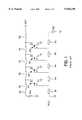
- Distributed amplifiersare known to be used for wide bandwidth applications. Examples of early distributed amplifiers formed with vacuum tubes are disclosed in: “Distributed Amplification”, by F. L. Ginzton, W. R. Hewlett, J. H. Jasberg, and J. D. Noe, PROC. IRE, Vol. 36, pp. 956-969, August 1948; “Principles and Design of Linear Active Circuits”, by M. S. Ghausi, Ch. 13, McGraw-Hill 1965; and British Patent No. 460,562, January 1937. With the development of the transistor, the vacuum tubes in the distributed amplifier circuits were replaced with common source field effect transistors (FET), for example, as disclosed in: “MESFET Distributed Amplifier Design Guidelines", by J. P.
- FETcommon source field effect transistors
- a plurality of FETs, 4 for example, 22, 24, 26 and 28,are connected in a common source configuration.
- input and output capacitances for each of the FETs 22, 24, 26 and 28,are combined with inductances 34-52 to form artificial transmission lines, generally identified with the reference numerals 30 and 32.
- the drain terminals of all the FETs 22, 24, 26 and 28are coupled together by way of the lumped or distributed inductances or transmission lines 34, 38, 42, and 46 and connected to an AC ground by way of a drain line termination impedance represented as the resistor R DT , which is generally chosen to match the characteristic impedance of the output line.
- each of the FETs 22, 24, 26 and 28are coupled together by way of the inductances 40, 44, 48 and 52 and terminated to an AC ground by way of a gate line termination resistance, illustrated as R gt , selected to be relatively equal to the characteristic impedance of the input transmission line.
- R gtgate line termination resistance
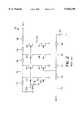
- a cascode configured deviceas generally illustrated in FIG. 2, and generally identified with the reference numeral 54 was developed.
- the known distributed amplifier 54shown without bias voltage and capacitors for grounding the line termination resistors for simplicity as discussed above, is shown with four stages, for example.
- Each stageincludes a pair of FETs 56, 58, 60, 62, 64, 66, 68, and 70, connected in a cascode configuration.
- the FETs 58, 62, 66 and 70are connected in a common source configuration and are used to drive the FETs 56, 60, 64 and 68, which, in turn, are connected in a common gate configuration.
- the drain terminals of the FETs 56, 60, 64 and 68are coupled together by way of the lumped inductances 72, 76, 80 and 84 and connected to an AC ground by way of a drain line termination resistance R DT .
- the gate terminals of the FETs 58, 62, 66 and 70are coupled together by way of the inductances 78, 82, 86 and 90 and connected to an AC ground by way of a gate line termination resistance R gt .
- the gate terminals each of the FETs 56, 60, 64 and 68are coupled together and connected to an AC ground by way of a capacitor 92.
- the cascode configuration illustrated in FIG. 2has an output resistance as a result of the common gate configuration that is much higher than a comparable common source device as illustrated in FIG. 1, which allows for a higher transconductance g m without degrading the output line by way of a large output conductance g o .
- some FETsespecially HEMTs
- have relatively low gate-to-drain breakdown voltagesi.e., 3-7 v.
- the output voltage swingto be relatively small, which limits the RF output power which can be achieved across a 50 W load.
- the present inventionrelates to a distributed amplifier formed from a high electron mobility transistor (HEMT) and a heterojunction bipolar transistor (HBT) configured in a cascode arrangement in which a common source FET, such as HEMT is used to drive an HBT in a common base configuration in order to provide increased RF output power relative to known distributed amplifiers.
- HEMThigh electron mobility transistor
- HBTheterojunction bipolar transistor
- FIG. 1is a simplified schematic diagram of a known common source FET distributed amplifier.
- FIG. 2is a simplified schematic diagram of a known FET cascode distributed amplifier.
- FIG. 3is a simplified schematic diagram of a HEMT-HBT cascode distributed amplifier in accordance with the present invention.
- the distributed amplifier in accordance with the present inventionis illustrated in FIG. 3 and generally identified with the reference numeral 94.
- the distributed amplifier 94is shown with AC grounding capacitors C 1 and C 2 as well as gate and drain bias voltages V DD and V GG .
- the distributed amplifier 94is formed with a plurality of stages, for example, four stages 96, 97, 99 and 101.
- Each stage 96, 97, 99 and 101includes a field effect transistor (FET), preferably, a high electron mobility transistor (HEMT) 102, 104, 106 and 108, having gate, drain and source terminals.
- Each stage 96, 97, 99 and 101further includes a heterojunction bipolar transistor (HBT) 110, 112, 114, 116 having base collector and emitter terminals.
- FETfield effect transistor
- HBTheterojunction bipolar transistor
- the HBTs 110, 112, 114 and 116are configured in a common base configuration.
- the base terminals of the HBTs 110, 112, 114 and 116are coupled to an AC ground by way of a bypass capacitor 118.
- the collector terminalsare coupled to inductances 120, 122, 124, 126 and 128 which, in conjunction with the capacitances of the HBTs 110, 112, 114 and 116 simulate what is known as a "constant k" transmission line 98.
- the collector terminals of the HBTs 110, 112, 114 and 116are connected to AC ground by way of a termination resistor R DT , selected to have a value generally equal to the characteristic impedance of the simulated transmission line 98.
- the collector terminalsare also coupled through the output transmission line to the output terminal OUT.
- each of the HBTs 110, 112, 114 and 116are connected to the drain terminals of each of the HEMTs 102, 104, 106 and 108.
- the source terminals of the HEMTs 102, 104, 106 and 108are all connected to ground, defining a common source configuration for the HEMTs.
- the gate terminals for each of the HEMTs 102, 104, 106 and 108are coupled together by way of a plurality of inductances or inductive transmission lines 130, 132, 134, 136 and 138 which, in conjunction with the gate capacitance of the HEMTs 102, 104, 106 and 108 form the simulated "constant k" transmission line 100.
- the gate terminals of the HEMTs 102, 104, 106 and 108are coupled together through the transmission line elements and terminated on one end in gate termination resistor, R gt , which is AC coupled to ground.
- the gate termination resistor R gtis selected to have a value nominally equal to the characteristic impedance of the transmission line 100.
- Each of the stages 96, 97, 99 and 101forms a cascode configuration with a common source HEMT 102, 104, 106 and 108 driving a common gate HBT 110, 112, 114 and 116. More or less stages can be used.
- the cascode configuration illustrated in FIG. 3has the potential for providing improved results over other known configurations in many respects.
- the input impedance of the common base HBT illustrated in FIG. 3is relatively smaller than that of the common gate FET illustrated in FIG. 2, due to the relatively higher transconductance of the HBT for a given bias current, the circuit in FIG. 3 provides for relatively better suppression of the Miller effect thus enabling independent design of the input and output lines.
- Another aspect of the distributed amplifier in accordance with the present inventionis that HBTs have high output resistance, due to the lack of any significant base width modulation. This is brought about by the high doped base region generally found in HBTS.
- the output resistanceis even higher still, allowing the device to form a near perfect "constant-k" transmission line at the output.
- the configurationprovides the potential for an increase in the number of distributed stages and thus provides the potential for higher gain.
- An important aspect of the present inventionis the relatively higher breakdown voltage of the HBT, which provides for increased RF output power.
- the overall breakdown voltageis not that of the HEMT, with a breakdown voltage BV GDO of approximately 3 V (for this particular process), but rather that of the common base HBT with a breakdown voltage BV CBO of approximately 22 v. Since by far the majority of the output voltage swing is across the common base HBT in a cascode, the small breakdown voltage of the HEMT is of no great consequence.
- the distributed amplifier 94is able to provide much larger voltage swings at the output and, thus, allows the circuit to be used in relatively broad band power applications. For example, if the voltage swing is twice as large at the output, an ⁇ 4 increase in RF power can be achieved.
- the HBTs in the distributed amplifier 94provide relatively broad band performance due to their common base connections.
- the, common base HBTeffectively functions as an impedance transformer and as a unity gain current amplifier, merely taking the current delivered by the HEMT and providing it to the load.
- the common base current gain cut off frequency f.sub. ⁇becomes the dominant high frequency figure of merit.
- the alpha cut-off frequency f.sub. ⁇is closely related to the common emitter short-circuit unity current gain frequency, f T and is affected in the same manner by the same geometric, doping and biasing parameters.
- the distributed amplifier 94includes HEMTs and HBTS.
- the HEMTis the best design choice for reducing input line losses due to its nearly perfect capacitive input, while the HBT is superior at the output because of its high output impedance dominated by a small capacitance.
- MMICmicrowave integrated circuit
Landscapes
- Engineering & Computer Science (AREA)
- Power Engineering (AREA)
- Microwave Amplifiers (AREA)
- Amplifiers (AREA)
Abstract
Description
Claims (15)
Priority Applications (2)
| Application Number | Priority Date | Filing Date | Title |
|---|---|---|---|
| US08/955,379US5920230A (en) | 1997-10-21 | 1997-10-21 | HEMT-HBT cascode distributed amplifier |
| JP10293723AJPH11195939A (en) | 1997-10-21 | 1998-10-15 | Hemt-hbt cascode distributed amplifier |
Applications Claiming Priority (1)
| Application Number | Priority Date | Filing Date | Title |
|---|---|---|---|
| US08/955,379US5920230A (en) | 1997-10-21 | 1997-10-21 | HEMT-HBT cascode distributed amplifier |
Publications (1)
| Publication Number | Publication Date |
|---|---|
| US5920230Atrue US5920230A (en) | 1999-07-06 |
Family
ID=25496745
Family Applications (1)
| Application Number | Title | Priority Date | Filing Date |
|---|---|---|---|
| US08/955,379Expired - LifetimeUS5920230A (en) | 1997-10-21 | 1997-10-21 | HEMT-HBT cascode distributed amplifier |
Country Status (2)
| Country | Link |
|---|---|
| US (1) | US5920230A (en) |
| JP (1) | JPH11195939A (en) |
Cited By (25)
| Publication number | Priority date | Publication date | Assignee | Title |
|---|---|---|---|---|
| US6377125B1 (en) | 2001-03-15 | 2002-04-23 | Motorola.Inc. | Distributed amplifier having separately biased sections |
| US6400227B1 (en)* | 2001-05-31 | 2002-06-04 | Analog Devices, Inc. | Stepped gain controlled RF driver amplifier in CMOS |
| US6433640B1 (en) | 2001-05-25 | 2002-08-13 | Motorola, Inc. | Methods and apparatus for amplifying a telecommunication signal |
| GB2373937A (en)* | 2001-03-27 | 2002-10-02 | Secr Defence | Improvements in travelling wave amplifiers |
| US6472941B2 (en)* | 2000-07-19 | 2002-10-29 | Fujitsu Limited | Distributed amplifier with terminating circuit capable of improving gain flatness at low frequencies |
| US6597243B1 (en)* | 2001-12-31 | 2003-07-22 | Agere Systems, Inc. | Distributed amplifier having a tapered transconductance architecture |
| WO2003084063A1 (en)* | 2002-03-28 | 2003-10-09 | Hrl Laboratories, Llc | High-efficiency, high output drive current switch with application to digital to analog conversion |
| US6747511B1 (en) | 2001-05-21 | 2004-06-08 | Euvis, Inc. | Distributed amplifier with pi-configuration analysis and synthesis lines |
| US20040124924A1 (en)* | 2002-07-23 | 2004-07-01 | Regis Claveau | Active load device that enables biasing of a very wide band distributed amplifier circuit with gain control |
| US20040130398A1 (en)* | 2003-01-02 | 2004-07-08 | Intel Corporation | Ultra wide band low noise amplifier and method |
| US20060108664A1 (en)* | 2004-11-03 | 2006-05-25 | Apostolos Samelis | Pre-matching of distributed and push-pull power transistors |
| US20060238269A1 (en)* | 2001-04-06 | 2006-10-26 | Nec Corporation | Reflection loss suppression circuit |
| US20070090879A1 (en)* | 2005-10-21 | 2007-04-26 | Northrop Grumman Corporation | Active input load wide bandwidth low noise hemt amplifier |
| EP1801968A1 (en)* | 2005-12-21 | 2007-06-27 | Thales | Broadband balun structure |
| US20070216485A1 (en)* | 2006-03-17 | 2007-09-20 | Kohei Fujii | Linear variable gain traveling wave amplifier |
| US20080238541A1 (en)* | 2007-03-31 | 2008-10-02 | Fasoli Luca G | Spatially distributed amplifier circuit |
| US7558140B2 (en) | 2007-03-31 | 2009-07-07 | Sandisk 3D Llc | Method for using a spatially distributed amplifier circuit |
| US20100052809A1 (en)* | 2008-08-29 | 2010-03-04 | Motorola, Inc. | Method and apparatus for adjusting load impedance of a distributed amplifier |
| FR2959077A1 (en)* | 2010-04-19 | 2011-10-21 | Alcatel Lucent | AMPLIFIER WITH LOW NOISE FACTOR, VARIABLE GAIN AND POWER |
| CN103199851A (en)* | 2013-03-19 | 2013-07-10 | 苏州朗宽电子技术有限公司 | Mixing common-source common-base circuit of metallic oxide field-effect tubes and bipolar transistors |
| US20140320211A1 (en)* | 2011-03-09 | 2014-10-30 | Hittite Microwave Corporation | Distributed amplifier with improved stabilization |
| US9524872B1 (en)* | 2009-02-03 | 2016-12-20 | Hrl Laboratories, Llc | Heterogeneous integrated circuits and devices thereof with a surrogate substrate and transferred semiconductor devices |
| US10778159B2 (en) | 2017-11-20 | 2020-09-15 | Murata Manufacturing Co., Ltd. | Power amplifier and compound semiconductor device |
| US11309852B2 (en) | 2017-11-20 | 2022-04-19 | Murata Manufacturing Co., Ltd. | Power amplifier and compound semiconductor device |
| US11515841B2 (en)* | 2019-05-31 | 2022-11-29 | Macom Technology Solutions Holdings, Inc. | DC coupled amplifier having pre-driver and bias control |
Families Citing this family (2)
| Publication number | Priority date | Publication date | Assignee | Title |
|---|---|---|---|---|
| JP5437506B2 (en)* | 2010-03-05 | 2014-03-12 | エプコス アクチエンゲゼルシャフト | Bias circuit having circuit unit, and differential amplifier circuit having first and second circuit units |
| JP7491378B2 (en)* | 2020-06-26 | 2024-05-28 | 日本電信電話株式会社 | Distributed Amplifier |
Citations (17)
| Publication number | Priority date | Publication date | Assignee | Title |
|---|---|---|---|---|
| GB460562A (en)* | 1935-07-24 | 1937-01-25 | William Spencer Percival | Improvements in and relating to thermionic valve circuits |
| US4276515A (en)* | 1978-03-01 | 1981-06-30 | Nippon Gakki Seizo Kabushiki Kaisha | Differential amplifier circuit arrangement with stabilized input impedance |
| US4550291A (en)* | 1983-10-03 | 1985-10-29 | Burr-Brown Corporation | Noise-free, die area efficient cascode circuit |
| US4586004A (en)* | 1983-06-27 | 1986-04-29 | Saber Technology Corp. | Logic and amplifier cells |
| US4688267A (en)* | 1984-11-21 | 1987-08-18 | Chown David P M | Optical fibre receiver |
| US4757276A (en)* | 1985-08-28 | 1988-07-12 | Kabushiki Kaisha Toshiba | Signal-processing circuit having a field-effect MOSFET and bipolar transistors |
| US4839609A (en)* | 1987-03-27 | 1989-06-13 | Kabushiki Kaisha Toshiba | Differential amplifier |
| US4901031A (en)* | 1989-01-17 | 1990-02-13 | Burr-Brown Corporation | Common-base, source-driven differential amplifier |
| US4992752A (en)* | 1989-06-09 | 1991-02-12 | Rockwell International | Method and apparatus for broadband impedance matching |
| US5032799A (en)* | 1989-10-04 | 1991-07-16 | Westinghouse Electric Corp. | Multistage cascode radio frequency amplifier |
| US5061903A (en)* | 1990-02-27 | 1991-10-29 | Grumman Aerospace Corporation | High voltage modified cascode circuit |
| US5066926A (en)* | 1990-06-26 | 1991-11-19 | Pacific Monolithics | Segmented cascode HBT for microwave-frequency power amplifiers |
| US5144266A (en)* | 1991-02-04 | 1992-09-01 | Motorola, Inc. | Broadband high frequency active MMIC circulator |
| US5227734A (en)* | 1991-08-26 | 1993-07-13 | Raytheon Company | Broadband bipolar transistor distributed amplifier |
| US5274342A (en)* | 1992-02-28 | 1993-12-28 | Hughes Aircraft Company | Microwave monolithic integrated circuit (MMIC) including distributed cascode bipolar transistor amplifier unit |
| US5304869A (en)* | 1992-04-17 | 1994-04-19 | Intel Corporation | BiCMOS digital amplifier |
| US5459433A (en)* | 1993-12-06 | 1995-10-17 | Siemens Aktiengesellschaft | Low-noise amplifier with reversible amplification in a cascode circuit |
- 1997
- 1997-10-21USUS08/955,379patent/US5920230A/ennot_activeExpired - Lifetime
- 1998
- 1998-10-15JPJP10293723Apatent/JPH11195939A/enactivePending
Patent Citations (17)
| Publication number | Priority date | Publication date | Assignee | Title |
|---|---|---|---|---|
| GB460562A (en)* | 1935-07-24 | 1937-01-25 | William Spencer Percival | Improvements in and relating to thermionic valve circuits |
| US4276515A (en)* | 1978-03-01 | 1981-06-30 | Nippon Gakki Seizo Kabushiki Kaisha | Differential amplifier circuit arrangement with stabilized input impedance |
| US4586004A (en)* | 1983-06-27 | 1986-04-29 | Saber Technology Corp. | Logic and amplifier cells |
| US4550291A (en)* | 1983-10-03 | 1985-10-29 | Burr-Brown Corporation | Noise-free, die area efficient cascode circuit |
| US4688267A (en)* | 1984-11-21 | 1987-08-18 | Chown David P M | Optical fibre receiver |
| US4757276A (en)* | 1985-08-28 | 1988-07-12 | Kabushiki Kaisha Toshiba | Signal-processing circuit having a field-effect MOSFET and bipolar transistors |
| US4839609A (en)* | 1987-03-27 | 1989-06-13 | Kabushiki Kaisha Toshiba | Differential amplifier |
| US4901031A (en)* | 1989-01-17 | 1990-02-13 | Burr-Brown Corporation | Common-base, source-driven differential amplifier |
| US4992752A (en)* | 1989-06-09 | 1991-02-12 | Rockwell International | Method and apparatus for broadband impedance matching |
| US5032799A (en)* | 1989-10-04 | 1991-07-16 | Westinghouse Electric Corp. | Multistage cascode radio frequency amplifier |
| US5061903A (en)* | 1990-02-27 | 1991-10-29 | Grumman Aerospace Corporation | High voltage modified cascode circuit |
| US5066926A (en)* | 1990-06-26 | 1991-11-19 | Pacific Monolithics | Segmented cascode HBT for microwave-frequency power amplifiers |
| US5144266A (en)* | 1991-02-04 | 1992-09-01 | Motorola, Inc. | Broadband high frequency active MMIC circulator |
| US5227734A (en)* | 1991-08-26 | 1993-07-13 | Raytheon Company | Broadband bipolar transistor distributed amplifier |
| US5274342A (en)* | 1992-02-28 | 1993-12-28 | Hughes Aircraft Company | Microwave monolithic integrated circuit (MMIC) including distributed cascode bipolar transistor amplifier unit |
| US5304869A (en)* | 1992-04-17 | 1994-04-19 | Intel Corporation | BiCMOS digital amplifier |
| US5459433A (en)* | 1993-12-06 | 1995-10-17 | Siemens Aktiengesellschaft | Low-noise amplifier with reversible amplification in a cascode circuit |
Non-Patent Citations (18)
| Title |
|---|
| "A Cascode Video Amplifier", Integrated Electronics, Sec. 16-10, pp. 565-567. |
| "Distributed Amplication", by E.L. Ginzton, W.R.Hewlett, J.H.Jasberg and J.D. Noe. |
| "Integrated Circuit Tuned Amplifier", Integrated Electronics, Sec. 16-9, pp. 558-564. |
| "MESFET Distributed Amplifier Design Guidelines", by J.B. Beyer, S.N. Prasad, R.C. Becker, J. E. Nordmann, and G,K, Hohenwarter, |
| "On Gain-Bainwidth Product for Distributed Amplifiers", by R.C. Becker and J.B. Beyer. |
| "Wideband Additive Amplifiers", Pentode Distributed Amplifiers, Chap. 13, pp. 334-358. |
| A Cascode Video Amplifier , Integrated Electronics, Sec. 16 10, pp. 565 567.* |
| Distributed Amplication , by E.L. Ginzton, W.R.Hewlett, J.H.Jasberg and J.D. Noe.* |
| IEEE Transactions on Microwave Theory and Techniques, vol. MTT 32, No. 2, Mar. 1984, pp. 268 275.* |
| IEEE Transactions on Microwave Theory and Techniques, vol. MTT 34, No. 6, Jun. 1986, pp. 736 738.* |
| IEEE Transactions on Microwave Theory and Techniques, vol. MTT-32, No. 2, Mar. 1984, pp. 268-275. |
| IEEE Transactions on Microwave Theory and Techniques, vol. MTT-34, No. 6, Jun. 1986, pp. 736-738. |
| Integrated Circuit Tuned Amplifier , Integrated Electronics, Sec. 16 9, pp. 558 564.* |
| MESFET Distributed Amplifier Design Guidelines , by J.B. Beyer, S.N. Prasad, R.C. Becker, J. E. Nordmann, and G,K, Hohenwarter,* |
| On Gain Bainwidth Product for Distributed Amplifiers , by R.C. Becker and J.B. Beyer.* |
| Proceedings of the I.R.E., Aug. 1948, pp. 956 969.* |
| Proceedings of the I.R.E., Aug. 1948, pp. 956-969. |
| Wideband Additive Amplifiers , Pentode Distributed Amplifiers, Chap. 13, pp. 334 358.* |
Cited By (46)
| Publication number | Priority date | Publication date | Assignee | Title |
|---|---|---|---|---|
| US6472941B2 (en)* | 2000-07-19 | 2002-10-29 | Fujitsu Limited | Distributed amplifier with terminating circuit capable of improving gain flatness at low frequencies |
| US6377125B1 (en) | 2001-03-15 | 2002-04-23 | Motorola.Inc. | Distributed amplifier having separately biased sections |
| US20040130390A1 (en)* | 2001-03-27 | 2004-07-08 | Zelley Christopher Andrew | Travelling wave amplifiers |
| US7142052B2 (en) | 2001-03-27 | 2006-11-28 | Qinetiq Limited | Travelling wave amplifiers |
| GB2373937A (en)* | 2001-03-27 | 2002-10-02 | Secr Defence | Improvements in travelling wave amplifiers |
| US7129804B2 (en) | 2001-04-06 | 2006-10-31 | Nec Corporation | Reflection loss suppression circuit |
| US20060238269A1 (en)* | 2001-04-06 | 2006-10-26 | Nec Corporation | Reflection loss suppression circuit |
| US7173502B2 (en) | 2001-04-06 | 2007-02-06 | Nec Corporation | Reflection loss suppression circuit |
| US6747511B1 (en) | 2001-05-21 | 2004-06-08 | Euvis, Inc. | Distributed amplifier with pi-configuration analysis and synthesis lines |
| US6433640B1 (en) | 2001-05-25 | 2002-08-13 | Motorola, Inc. | Methods and apparatus for amplifying a telecommunication signal |
| US6400227B1 (en)* | 2001-05-31 | 2002-06-04 | Analog Devices, Inc. | Stepped gain controlled RF driver amplifier in CMOS |
| US6597243B1 (en)* | 2001-12-31 | 2003-07-22 | Agere Systems, Inc. | Distributed amplifier having a tapered transconductance architecture |
| WO2003084063A1 (en)* | 2002-03-28 | 2003-10-09 | Hrl Laboratories, Llc | High-efficiency, high output drive current switch with application to digital to analog conversion |
| US6894566B2 (en)* | 2002-07-23 | 2005-05-17 | Da-Lightcom | Active load device that enables biasing of a very wide band distributed amplifier circuit with gain control |
| US20040124924A1 (en)* | 2002-07-23 | 2004-07-01 | Regis Claveau | Active load device that enables biasing of a very wide band distributed amplifier circuit with gain control |
| US6806777B2 (en)* | 2003-01-02 | 2004-10-19 | Intel Corporation | Ultra wide band low noise amplifier and method |
| US20040130398A1 (en)* | 2003-01-02 | 2004-07-08 | Intel Corporation | Ultra wide band low noise amplifier and method |
| US20060108664A1 (en)* | 2004-11-03 | 2006-05-25 | Apostolos Samelis | Pre-matching of distributed and push-pull power transistors |
| US7268627B2 (en)* | 2004-11-03 | 2007-09-11 | Theta Microelectronics, Inc. | Pre-matching of distributed and push-pull power transistors |
| DE112006002920T5 (en) | 2005-10-21 | 2008-10-30 | Northrop Grumman Corp., Los Angeles | Low-noise HEMT amplifier with high bandwidth and active input load |
| US20070090879A1 (en)* | 2005-10-21 | 2007-04-26 | Northrop Grumman Corporation | Active input load wide bandwidth low noise hemt amplifier |
| US7612610B2 (en) | 2005-10-21 | 2009-11-03 | Northrop Grumman Corporation | Active input load wide bandwidth low noise HEMT amplifier |
| EP1801968A1 (en)* | 2005-12-21 | 2007-06-27 | Thales | Broadband balun structure |
| US7400200B2 (en)* | 2006-03-17 | 2008-07-15 | Avago Technologies Wireless Ip Pte Ltd | Linear variable gain traveling wave amplifier |
| US20070216485A1 (en)* | 2006-03-17 | 2007-09-20 | Kohei Fujii | Linear variable gain traveling wave amplifier |
| GB2436179B (en)* | 2006-03-17 | 2010-10-20 | Avago Technologies Wireless Ip | Amplifier circuits |
| US20080238541A1 (en)* | 2007-03-31 | 2008-10-02 | Fasoli Luca G | Spatially distributed amplifier circuit |
| US7554406B2 (en)* | 2007-03-31 | 2009-06-30 | Sandisk 3D Llc | Spatially distributed amplifier circuit |
| US7558140B2 (en) | 2007-03-31 | 2009-07-07 | Sandisk 3D Llc | Method for using a spatially distributed amplifier circuit |
| US20100052809A1 (en)* | 2008-08-29 | 2010-03-04 | Motorola, Inc. | Method and apparatus for adjusting load impedance of a distributed amplifier |
| WO2010025027A3 (en)* | 2008-08-29 | 2010-05-14 | Motorola, Inc. | Method and apparatus for adjusting load impedance of a distributed amplifier |
| US7880558B2 (en) | 2008-08-29 | 2011-02-01 | Motorola, Inc. | Method and apparatus for adjusting load impedance of a distributed amplifier |
| US9524872B1 (en)* | 2009-02-03 | 2016-12-20 | Hrl Laboratories, Llc | Heterogeneous integrated circuits and devices thereof with a surrogate substrate and transferred semiconductor devices |
| US8928414B2 (en)* | 2010-04-19 | 2015-01-06 | Alcatel Lucent | Power amplifier with low noise figure and voltage variable gain |
| US20130093520A1 (en)* | 2010-04-19 | 2013-04-18 | Alcatel Lucent | Power amplifier with low noise figure and voltage variable gain |
| FR2959077A1 (en)* | 2010-04-19 | 2011-10-21 | Alcatel Lucent | AMPLIFIER WITH LOW NOISE FACTOR, VARIABLE GAIN AND POWER |
| WO2011131625A1 (en)* | 2010-04-19 | 2011-10-27 | Alcatel Lucent | Power amplifier with low noise figure and voltage variable gain |
| US20140320211A1 (en)* | 2011-03-09 | 2014-10-30 | Hittite Microwave Corporation | Distributed amplifier with improved stabilization |
| US9425752B2 (en)* | 2011-03-09 | 2016-08-23 | Hittite Microwave Llc | Distributed amplifier with improved stabilization |
| US10122325B2 (en) | 2011-03-09 | 2018-11-06 | Hittite Microwave Llc | Distributed amplifier with improved stabilization |
| US10164579B2 (en) | 2011-03-09 | 2018-12-25 | Hittite Microwave Llc | Distributed amplifier |
| CN103199851A (en)* | 2013-03-19 | 2013-07-10 | 苏州朗宽电子技术有限公司 | Mixing common-source common-base circuit of metallic oxide field-effect tubes and bipolar transistors |
| US10778159B2 (en) | 2017-11-20 | 2020-09-15 | Murata Manufacturing Co., Ltd. | Power amplifier and compound semiconductor device |
| US11309852B2 (en) | 2017-11-20 | 2022-04-19 | Murata Manufacturing Co., Ltd. | Power amplifier and compound semiconductor device |
| US11515841B2 (en)* | 2019-05-31 | 2022-11-29 | Macom Technology Solutions Holdings, Inc. | DC coupled amplifier having pre-driver and bias control |
| US12113483B2 (en) | 2019-05-31 | 2024-10-08 | Macom Technologies Solutions Holdings, Inc. | DC coupled amplifier having pre-driver and bias control |
Also Published As
| Publication number | Publication date |
|---|---|
| JPH11195939A (en) | 1999-07-21 |
Similar Documents
| Publication | Publication Date | Title |
|---|---|---|
| US5920230A (en) | HEMT-HBT cascode distributed amplifier | |
| US6400226B2 (en) | Distributed amplifier with improved flatness of frequency characteristic | |
| Ezzeddine et al. | The high voltage/high power FET (HiVP) | |
| JP5296181B2 (en) | Transistor amplifier with reduced parasitic oscillation | |
| US5486787A (en) | Monolithic microwave integrated circuit apparatus | |
| US5227734A (en) | Broadband bipolar transistor distributed amplifier | |
| KR970060674A (en) | Low Noise Amplifiers and Monolithic Microwave Integrated Circuits | |
| US5028879A (en) | Compensation of the gate loading loss for travelling wave power amplifiers | |
| US5838031A (en) | Low noise-high linearity HEMT-HBT composite | |
| US7482874B2 (en) | Non-uniform distributed multi-stage circuits | |
| JP3131931B2 (en) | High frequency high power amplifier | |
| JPH11136111A5 (en) | ||
| JP3175823B2 (en) | High frequency amplifier | |
| US5349306A (en) | Apparatus and method for high performance wide-band power amplifier monolithic microwave integrated circuits | |
| CN111262534B (en) | Self-adaptive bias circuit for power amplifier chip | |
| US5559472A (en) | Loss compensated gain cell for distributed amplifiers | |
| Brown et al. | Broadband GaN DHFET traveling wave amplifiers with up to 120 GHz bandwidth | |
| CA1210093A (en) | High frequency amplifier | |
| CN1159841C (en) | RF amplifier with gain control | |
| US8633771B2 (en) | Power amplifier | |
| CN117375544A (en) | Ultra-wideband distributed low-noise amplifier with triple cascade structure | |
| US20030048138A1 (en) | High frequency power amplifier circuit | |
| US6664842B1 (en) | FET active load and current source | |
| US7368971B2 (en) | High power, high frequency switch circuits using strings of power transistors | |
| JP2021090168A (en) | Power amplifier circuit |
Legal Events
| Date | Code | Title | Description |
|---|---|---|---|
| AS | Assignment | Owner name:TRW INC., CALIFORNIA Free format text:ASSIGNMENT OF ASSIGNORS INTEREST;ASSIGNOR:BEALL, WENDELL G.;REEL/FRAME:008860/0549 Effective date:19971017 | |
| STCF | Information on status: patent grant | Free format text:PATENTED CASE | |
| FPAY | Fee payment | Year of fee payment:4 | |
| AS | Assignment | Owner name:NORTHROP GRUMMAN CORPORATION, CALIFORNIA Free format text:ASSIGNMENT OF ASSIGNORS INTEREST;ASSIGNOR:TRW, INC. N/K/A NORTHROP GRUMMAN SPACE AND MISSION SYSTEMS CORPORATION, AN OHIO CORPORATION;REEL/FRAME:013751/0849 Effective date:20030122 Owner name:NORTHROP GRUMMAN CORPORATION,CALIFORNIA Free format text:ASSIGNMENT OF ASSIGNORS INTEREST;ASSIGNOR:TRW, INC. N/K/A NORTHROP GRUMMAN SPACE AND MISSION SYSTEMS CORPORATION, AN OHIO CORPORATION;REEL/FRAME:013751/0849 Effective date:20030122 | |
| FPAY | Fee payment | Year of fee payment:8 | |
| FEPP | Fee payment procedure | Free format text:PAYOR NUMBER ASSIGNED (ORIGINAL EVENT CODE: ASPN); ENTITY STATUS OF PATENT OWNER: LARGE ENTITY | |
| AS | Assignment | Owner name:NORTHROP GRUMMAN SPACE & MISSION SYSTEMS CORP.,CAL Free format text:ASSIGNMENT OF ASSIGNORS INTEREST;ASSIGNOR:NORTHROP GRUMMAN CORPORTION;REEL/FRAME:023699/0551 Effective date:20091125 Owner name:NORTHROP GRUMMAN SPACE & MISSION SYSTEMS CORP., CA Free format text:ASSIGNMENT OF ASSIGNORS INTEREST;ASSIGNOR:NORTHROP GRUMMAN CORPORTION;REEL/FRAME:023699/0551 Effective date:20091125 | |
| AS | Assignment | Owner name:NORTHROP GRUMMAN SYSTEMS CORPORATION,CALIFORNIA Free format text:ASSIGNMENT OF ASSIGNORS INTEREST;ASSIGNOR:NORTHROP GRUMMAN SPACE & MISSION SYSTEMS CORP.;REEL/FRAME:023915/0446 Effective date:20091210 Owner name:NORTHROP GRUMMAN SYSTEMS CORPORATION, CALIFORNIA Free format text:ASSIGNMENT OF ASSIGNORS INTEREST;ASSIGNOR:NORTHROP GRUMMAN SPACE & MISSION SYSTEMS CORP.;REEL/FRAME:023915/0446 Effective date:20091210 | |
| FPAY | Fee payment | Year of fee payment:12 |