US5920126A - Semiconductor device including a flip-chip substrate - Google Patents
Semiconductor device including a flip-chip substrateDownload PDFInfo
- Publication number
- US5920126A US5920126AUS09/162,770US16277098AUS5920126AUS 5920126 AUS5920126 AUS 5920126AUS 16277098 AUS16277098 AUS 16277098AUS 5920126 AUS5920126 AUS 5920126A
- Authority
- US
- United States
- Prior art keywords
- flip
- cutout
- conductor pattern
- chip
- chip substrate
- Prior art date
- Legal status (The legal status is an assumption and is not a legal conclusion. Google has not performed a legal analysis and makes no representation as to the accuracy of the status listed.)
- Expired - Lifetime
Links
Images


Classifications
- H—ELECTRICITY
- H01—ELECTRIC ELEMENTS
- H01L—SEMICONDUCTOR DEVICES NOT COVERED BY CLASS H10
- H01L24/00—Arrangements for connecting or disconnecting semiconductor or solid-state bodies; Methods or apparatus related thereto
- H01L24/01—Means for bonding being attached to, or being formed on, the surface to be connected, e.g. chip-to-package, die-attach, "first-level" interconnects; Manufacturing methods related thereto
- H01L24/26—Layer connectors, e.g. plate connectors, solder or adhesive layers; Manufacturing methods related thereto
- H01L24/31—Structure, shape, material or disposition of the layer connectors after the connecting process
- H01L24/32—Structure, shape, material or disposition of the layer connectors after the connecting process of an individual layer connector
- H—ELECTRICITY
- H01—ELECTRIC ELEMENTS
- H01L—SEMICONDUCTOR DEVICES NOT COVERED BY CLASS H10
- H01L21/00—Processes or apparatus adapted for the manufacture or treatment of semiconductor or solid state devices or of parts thereof
- H01L21/02—Manufacture or treatment of semiconductor devices or of parts thereof
- H01L21/04—Manufacture or treatment of semiconductor devices or of parts thereof the devices having potential barriers, e.g. a PN junction, depletion layer or carrier concentration layer
- H01L21/50—Assembly of semiconductor devices using processes or apparatus not provided for in a single one of the groups H01L21/18 - H01L21/326 or H10D48/04 - H10D48/07 e.g. sealing of a cap to a base of a container
- H01L21/56—Encapsulations, e.g. encapsulation layers, coatings
- H01L21/563—Encapsulation of active face of flip-chip device, e.g. underfilling or underencapsulation of flip-chip, encapsulation preform on chip or mounting substrate
- H—ELECTRICITY
- H01—ELECTRIC ELEMENTS
- H01L—SEMICONDUCTOR DEVICES NOT COVERED BY CLASS H10
- H01L24/00—Arrangements for connecting or disconnecting semiconductor or solid-state bodies; Methods or apparatus related thereto
- H01L24/01—Means for bonding being attached to, or being formed on, the surface to be connected, e.g. chip-to-package, die-attach, "first-level" interconnects; Manufacturing methods related thereto
- H01L24/10—Bump connectors ; Manufacturing methods related thereto
- H01L24/15—Structure, shape, material or disposition of the bump connectors after the connecting process
- H01L24/16—Structure, shape, material or disposition of the bump connectors after the connecting process of an individual bump connector
- H—ELECTRICITY
- H01—ELECTRIC ELEMENTS
- H01L—SEMICONDUCTOR DEVICES NOT COVERED BY CLASS H10
- H01L24/00—Arrangements for connecting or disconnecting semiconductor or solid-state bodies; Methods or apparatus related thereto
- H01L24/01—Means for bonding being attached to, or being formed on, the surface to be connected, e.g. chip-to-package, die-attach, "first-level" interconnects; Manufacturing methods related thereto
- H01L24/26—Layer connectors, e.g. plate connectors, solder or adhesive layers; Manufacturing methods related thereto
- H01L24/28—Structure, shape, material or disposition of the layer connectors prior to the connecting process
- H01L24/29—Structure, shape, material or disposition of the layer connectors prior to the connecting process of an individual layer connector
- H—ELECTRICITY
- H01—ELECTRIC ELEMENTS
- H01L—SEMICONDUCTOR DEVICES NOT COVERED BY CLASS H10
- H01L2224/00—Indexing scheme for arrangements for connecting or disconnecting semiconductor or solid-state bodies and methods related thereto as covered by H01L24/00
- H01L2224/01—Means for bonding being attached to, or being formed on, the surface to be connected, e.g. chip-to-package, die-attach, "first-level" interconnects; Manufacturing methods related thereto
- H01L2224/10—Bump connectors; Manufacturing methods related thereto
- H01L2224/11—Manufacturing methods
- H01L2224/113—Manufacturing methods by local deposition of the material of the bump connector
- H01L2224/1133—Manufacturing methods by local deposition of the material of the bump connector in solid form
- H01L2224/1134—Stud bumping, i.e. using a wire-bonding apparatus
- H—ELECTRICITY
- H01—ELECTRIC ELEMENTS
- H01L—SEMICONDUCTOR DEVICES NOT COVERED BY CLASS H10
- H01L2224/00—Indexing scheme for arrangements for connecting or disconnecting semiconductor or solid-state bodies and methods related thereto as covered by H01L24/00
- H01L2224/01—Means for bonding being attached to, or being formed on, the surface to be connected, e.g. chip-to-package, die-attach, "first-level" interconnects; Manufacturing methods related thereto
- H01L2224/10—Bump connectors; Manufacturing methods related thereto
- H01L2224/12—Structure, shape, material or disposition of the bump connectors prior to the connecting process
- H01L2224/13—Structure, shape, material or disposition of the bump connectors prior to the connecting process of an individual bump connector
- H01L2224/13001—Core members of the bump connector
- H01L2224/13099—Material
- H01L2224/131—Material with a principal constituent of the material being a metal or a metalloid, e.g. boron [B], silicon [Si], germanium [Ge], arsenic [As], antimony [Sb], tellurium [Te] and polonium [Po], and alloys thereof
- H01L2224/13101—Material with a principal constituent of the material being a metal or a metalloid, e.g. boron [B], silicon [Si], germanium [Ge], arsenic [As], antimony [Sb], tellurium [Te] and polonium [Po], and alloys thereof the principal constituent melting at a temperature of less than 400°C
- H01L2224/13111—Tin [Sn] as principal constituent
- H—ELECTRICITY
- H01—ELECTRIC ELEMENTS
- H01L—SEMICONDUCTOR DEVICES NOT COVERED BY CLASS H10
- H01L2224/00—Indexing scheme for arrangements for connecting or disconnecting semiconductor or solid-state bodies and methods related thereto as covered by H01L24/00
- H01L2224/01—Means for bonding being attached to, or being formed on, the surface to be connected, e.g. chip-to-package, die-attach, "first-level" interconnects; Manufacturing methods related thereto
- H01L2224/10—Bump connectors; Manufacturing methods related thereto
- H01L2224/12—Structure, shape, material or disposition of the bump connectors prior to the connecting process
- H01L2224/13—Structure, shape, material or disposition of the bump connectors prior to the connecting process of an individual bump connector
- H01L2224/13001—Core members of the bump connector
- H01L2224/13099—Material
- H01L2224/131—Material with a principal constituent of the material being a metal or a metalloid, e.g. boron [B], silicon [Si], germanium [Ge], arsenic [As], antimony [Sb], tellurium [Te] and polonium [Po], and alloys thereof
- H01L2224/13138—Material with a principal constituent of the material being a metal or a metalloid, e.g. boron [B], silicon [Si], germanium [Ge], arsenic [As], antimony [Sb], tellurium [Te] and polonium [Po], and alloys thereof the principal constituent melting at a temperature of greater than or equal to 950°C and less than 1550°C
- H01L2224/13144—Gold [Au] as principal constituent
- H—ELECTRICITY
- H01—ELECTRIC ELEMENTS
- H01L—SEMICONDUCTOR DEVICES NOT COVERED BY CLASS H10
- H01L2224/00—Indexing scheme for arrangements for connecting or disconnecting semiconductor or solid-state bodies and methods related thereto as covered by H01L24/00
- H01L2224/01—Means for bonding being attached to, or being formed on, the surface to be connected, e.g. chip-to-package, die-attach, "first-level" interconnects; Manufacturing methods related thereto
- H01L2224/10—Bump connectors; Manufacturing methods related thereto
- H01L2224/15—Structure, shape, material or disposition of the bump connectors after the connecting process
- H01L2224/16—Structure, shape, material or disposition of the bump connectors after the connecting process of an individual bump connector
- H01L2224/161—Disposition
- H01L2224/16151—Disposition the bump connector connecting between a semiconductor or solid-state body and an item not being a semiconductor or solid-state body, e.g. chip-to-substrate, chip-to-passive
- H01L2224/16221—Disposition the bump connector connecting between a semiconductor or solid-state body and an item not being a semiconductor or solid-state body, e.g. chip-to-substrate, chip-to-passive the body and the item being stacked
- H01L2224/16225—Disposition the bump connector connecting between a semiconductor or solid-state body and an item not being a semiconductor or solid-state body, e.g. chip-to-substrate, chip-to-passive the body and the item being stacked the item being non-metallic, e.g. insulating substrate with or without metallisation
- H—ELECTRICITY
- H01—ELECTRIC ELEMENTS
- H01L—SEMICONDUCTOR DEVICES NOT COVERED BY CLASS H10
- H01L2224/00—Indexing scheme for arrangements for connecting or disconnecting semiconductor or solid-state bodies and methods related thereto as covered by H01L24/00
- H01L2224/01—Means for bonding being attached to, or being formed on, the surface to be connected, e.g. chip-to-package, die-attach, "first-level" interconnects; Manufacturing methods related thereto
- H01L2224/26—Layer connectors, e.g. plate connectors, solder or adhesive layers; Manufacturing methods related thereto
- H01L2224/27—Manufacturing methods
- H01L2224/27011—Involving a permanent auxiliary member, i.e. a member which is left at least partly in the finished device, e.g. coating, dummy feature
- H01L2224/27013—Involving a permanent auxiliary member, i.e. a member which is left at least partly in the finished device, e.g. coating, dummy feature for holding or confining the layer connector, e.g. solder flow barrier
- H—ELECTRICITY
- H01—ELECTRIC ELEMENTS
- H01L—SEMICONDUCTOR DEVICES NOT COVERED BY CLASS H10
- H01L2224/00—Indexing scheme for arrangements for connecting or disconnecting semiconductor or solid-state bodies and methods related thereto as covered by H01L24/00
- H01L2224/01—Means for bonding being attached to, or being formed on, the surface to be connected, e.g. chip-to-package, die-attach, "first-level" interconnects; Manufacturing methods related thereto
- H01L2224/26—Layer connectors, e.g. plate connectors, solder or adhesive layers; Manufacturing methods related thereto
- H01L2224/28—Structure, shape, material or disposition of the layer connectors prior to the connecting process
- H01L2224/29—Structure, shape, material or disposition of the layer connectors prior to the connecting process of an individual layer connector
- H01L2224/29001—Core members of the layer connector
- H01L2224/29099—Material
- H01L2224/291—Material with a principal constituent of the material being a metal or a metalloid, e.g. boron [B], silicon [Si], germanium [Ge], arsenic [As], antimony [Sb], tellurium [Te] and polonium [Po], and alloys thereof
- H01L2224/29101—Material with a principal constituent of the material being a metal or a metalloid, e.g. boron [B], silicon [Si], germanium [Ge], arsenic [As], antimony [Sb], tellurium [Te] and polonium [Po], and alloys thereof the principal constituent melting at a temperature of less than 400°C
- H01L2224/29111—Tin [Sn] as principal constituent
- H—ELECTRICITY
- H01—ELECTRIC ELEMENTS
- H01L—SEMICONDUCTOR DEVICES NOT COVERED BY CLASS H10
- H01L2224/00—Indexing scheme for arrangements for connecting or disconnecting semiconductor or solid-state bodies and methods related thereto as covered by H01L24/00
- H01L2224/01—Means for bonding being attached to, or being formed on, the surface to be connected, e.g. chip-to-package, die-attach, "first-level" interconnects; Manufacturing methods related thereto
- H01L2224/26—Layer connectors, e.g. plate connectors, solder or adhesive layers; Manufacturing methods related thereto
- H01L2224/28—Structure, shape, material or disposition of the layer connectors prior to the connecting process
- H01L2224/29—Structure, shape, material or disposition of the layer connectors prior to the connecting process of an individual layer connector
- H01L2224/29001—Core members of the layer connector
- H01L2224/29099—Material
- H01L2224/2919—Material with a principal constituent of the material being a polymer, e.g. polyester, phenolic based polymer, epoxy
- H—ELECTRICITY
- H01—ELECTRIC ELEMENTS
- H01L—SEMICONDUCTOR DEVICES NOT COVERED BY CLASS H10
- H01L2224/00—Indexing scheme for arrangements for connecting or disconnecting semiconductor or solid-state bodies and methods related thereto as covered by H01L24/00
- H01L2224/01—Means for bonding being attached to, or being formed on, the surface to be connected, e.g. chip-to-package, die-attach, "first-level" interconnects; Manufacturing methods related thereto
- H01L2224/26—Layer connectors, e.g. plate connectors, solder or adhesive layers; Manufacturing methods related thereto
- H01L2224/31—Structure, shape, material or disposition of the layer connectors after the connecting process
- H01L2224/32—Structure, shape, material or disposition of the layer connectors after the connecting process of an individual layer connector
- H01L2224/321—Disposition
- H01L2224/32151—Disposition the layer connector connecting between a semiconductor or solid-state body and an item not being a semiconductor or solid-state body, e.g. chip-to-substrate, chip-to-passive
- H01L2224/32221—Disposition the layer connector connecting between a semiconductor or solid-state body and an item not being a semiconductor or solid-state body, e.g. chip-to-substrate, chip-to-passive the body and the item being stacked
- H01L2224/32225—Disposition the layer connector connecting between a semiconductor or solid-state body and an item not being a semiconductor or solid-state body, e.g. chip-to-substrate, chip-to-passive the body and the item being stacked the item being non-metallic, e.g. insulating substrate with or without metallisation
- H—ELECTRICITY
- H01—ELECTRIC ELEMENTS
- H01L—SEMICONDUCTOR DEVICES NOT COVERED BY CLASS H10
- H01L2224/00—Indexing scheme for arrangements for connecting or disconnecting semiconductor or solid-state bodies and methods related thereto as covered by H01L24/00
- H01L2224/73—Means for bonding being of different types provided for in two or more of groups H01L2224/10, H01L2224/18, H01L2224/26, H01L2224/34, H01L2224/42, H01L2224/50, H01L2224/63, H01L2224/71
- H01L2224/732—Location after the connecting process
- H01L2224/73201—Location after the connecting process on the same surface
- H01L2224/73203—Bump and layer connectors
- H01L2224/73204—Bump and layer connectors the bump connector being embedded into the layer connector
- H—ELECTRICITY
- H01—ELECTRIC ELEMENTS
- H01L—SEMICONDUCTOR DEVICES NOT COVERED BY CLASS H10
- H01L2224/00—Indexing scheme for arrangements for connecting or disconnecting semiconductor or solid-state bodies and methods related thereto as covered by H01L24/00
- H01L2224/80—Methods for connecting semiconductor or other solid state bodies using means for bonding being attached to, or being formed on, the surface to be connected
- H01L2224/83—Methods for connecting semiconductor or other solid state bodies using means for bonding being attached to, or being formed on, the surface to be connected using a layer connector
- H01L2224/83009—Pre-treatment of the layer connector or the bonding area
- H01L2224/83051—Forming additional members, e.g. dam structures
- H—ELECTRICITY
- H01—ELECTRIC ELEMENTS
- H01L—SEMICONDUCTOR DEVICES NOT COVERED BY CLASS H10
- H01L2224/00—Indexing scheme for arrangements for connecting or disconnecting semiconductor or solid-state bodies and methods related thereto as covered by H01L24/00
- H01L2224/80—Methods for connecting semiconductor or other solid state bodies using means for bonding being attached to, or being formed on, the surface to be connected
- H01L2224/83—Methods for connecting semiconductor or other solid state bodies using means for bonding being attached to, or being formed on, the surface to be connected using a layer connector
- H01L2224/831—Methods for connecting semiconductor or other solid state bodies using means for bonding being attached to, or being formed on, the surface to be connected using a layer connector the layer connector being supplied to the parts to be connected in the bonding apparatus
- H01L2224/83102—Methods for connecting semiconductor or other solid state bodies using means for bonding being attached to, or being formed on, the surface to be connected using a layer connector the layer connector being supplied to the parts to be connected in the bonding apparatus using surface energy, e.g. capillary forces
- H—ELECTRICITY
- H01—ELECTRIC ELEMENTS
- H01L—SEMICONDUCTOR DEVICES NOT COVERED BY CLASS H10
- H01L2224/00—Indexing scheme for arrangements for connecting or disconnecting semiconductor or solid-state bodies and methods related thereto as covered by H01L24/00
- H01L2224/91—Methods for connecting semiconductor or solid state bodies including different methods provided for in two or more of groups H01L2224/80 - H01L2224/90
- H01L2224/92—Specific sequence of method steps
- H01L2224/921—Connecting a surface with connectors of different types
- H01L2224/9212—Sequential connecting processes
- H01L2224/92122—Sequential connecting processes the first connecting process involving a bump connector
- H01L2224/92125—Sequential connecting processes the first connecting process involving a bump connector the second connecting process involving a layer connector
- H—ELECTRICITY
- H01—ELECTRIC ELEMENTS
- H01L—SEMICONDUCTOR DEVICES NOT COVERED BY CLASS H10
- H01L2924/00—Indexing scheme for arrangements or methods for connecting or disconnecting semiconductor or solid-state bodies as covered by H01L24/00
- H01L2924/0001—Technical content checked by a classifier
- H01L2924/00013—Fully indexed content
- H—ELECTRICITY
- H01—ELECTRIC ELEMENTS
- H01L—SEMICONDUCTOR DEVICES NOT COVERED BY CLASS H10
- H01L2924/00—Indexing scheme for arrangements or methods for connecting or disconnecting semiconductor or solid-state bodies as covered by H01L24/00
- H01L2924/01—Chemical elements
- H01L2924/01029—Copper [Cu]
- H—ELECTRICITY
- H01—ELECTRIC ELEMENTS
- H01L—SEMICONDUCTOR DEVICES NOT COVERED BY CLASS H10
- H01L2924/00—Indexing scheme for arrangements or methods for connecting or disconnecting semiconductor or solid-state bodies as covered by H01L24/00
- H01L2924/01—Chemical elements
- H01L2924/01033—Arsenic [As]
- H—ELECTRICITY
- H01—ELECTRIC ELEMENTS
- H01L—SEMICONDUCTOR DEVICES NOT COVERED BY CLASS H10
- H01L2924/00—Indexing scheme for arrangements or methods for connecting or disconnecting semiconductor or solid-state bodies as covered by H01L24/00
- H01L2924/01—Chemical elements
- H01L2924/01039—Yttrium [Y]
- H—ELECTRICITY
- H01—ELECTRIC ELEMENTS
- H01L—SEMICONDUCTOR DEVICES NOT COVERED BY CLASS H10
- H01L2924/00—Indexing scheme for arrangements or methods for connecting or disconnecting semiconductor or solid-state bodies as covered by H01L24/00
- H01L2924/01—Chemical elements
- H01L2924/01047—Silver [Ag]
- H—ELECTRICITY
- H01—ELECTRIC ELEMENTS
- H01L—SEMICONDUCTOR DEVICES NOT COVERED BY CLASS H10
- H01L2924/00—Indexing scheme for arrangements or methods for connecting or disconnecting semiconductor or solid-state bodies as covered by H01L24/00
- H01L2924/01—Chemical elements
- H01L2924/0105—Tin [Sn]
- H—ELECTRICITY
- H01—ELECTRIC ELEMENTS
- H01L—SEMICONDUCTOR DEVICES NOT COVERED BY CLASS H10
- H01L2924/00—Indexing scheme for arrangements or methods for connecting or disconnecting semiconductor or solid-state bodies as covered by H01L24/00
- H01L2924/01—Chemical elements
- H01L2924/01079—Gold [Au]
- H—ELECTRICITY
- H01—ELECTRIC ELEMENTS
- H01L—SEMICONDUCTOR DEVICES NOT COVERED BY CLASS H10
- H01L2924/00—Indexing scheme for arrangements or methods for connecting or disconnecting semiconductor or solid-state bodies as covered by H01L24/00
- H01L2924/013—Alloys
- H01L2924/0132—Binary Alloys
- H—ELECTRICITY
- H01—ELECTRIC ELEMENTS
- H01L—SEMICONDUCTOR DEVICES NOT COVERED BY CLASS H10
- H01L2924/00—Indexing scheme for arrangements or methods for connecting or disconnecting semiconductor or solid-state bodies as covered by H01L24/00
- H01L2924/013—Alloys
- H01L2924/014—Solder alloys
- H—ELECTRICITY
- H01—ELECTRIC ELEMENTS
- H01L—SEMICONDUCTOR DEVICES NOT COVERED BY CLASS H10
- H01L2924/00—Indexing scheme for arrangements or methods for connecting or disconnecting semiconductor or solid-state bodies as covered by H01L24/00
- H01L2924/15—Details of package parts other than the semiconductor or other solid state devices to be connected
- H01L2924/151—Die mounting substrate
- H01L2924/1517—Multilayer substrate
- H—ELECTRICITY
- H01—ELECTRIC ELEMENTS
- H01L—SEMICONDUCTOR DEVICES NOT COVERED BY CLASS H10
- H01L2924/00—Indexing scheme for arrangements or methods for connecting or disconnecting semiconductor or solid-state bodies as covered by H01L24/00
- H01L2924/15—Details of package parts other than the semiconductor or other solid state devices to be connected
- H01L2924/151—Die mounting substrate
- H01L2924/153—Connection portion
- H01L2924/1531—Connection portion the connection portion being formed only on the surface of the substrate opposite to the die mounting surface
- H01L2924/15311—Connection portion the connection portion being formed only on the surface of the substrate opposite to the die mounting surface being a ball array, e.g. BGA
- H—ELECTRICITY
- H01—ELECTRIC ELEMENTS
- H01L—SEMICONDUCTOR DEVICES NOT COVERED BY CLASS H10
- H01L2924/00—Indexing scheme for arrangements or methods for connecting or disconnecting semiconductor or solid-state bodies as covered by H01L24/00
- H01L2924/15—Details of package parts other than the semiconductor or other solid state devices to be connected
- H01L2924/151—Die mounting substrate
- H01L2924/156—Material
- H01L2924/1579—Material with a principal constituent of the material being a polymer, e.g. polyester, phenolic based polymer, epoxy
Definitions
- the present inventiongenerally relates to semiconductor devices and more particularly to a semiconductor device including a semiconductor chip mounted on a flip-chip substrate.
- Semiconductor devices for use in electronic apparatusesare provided generally in the form of an interconnection substrate carrying thereon one or more semiconductor chips.
- the semiconductor devicesWith increasing demand for high performance operation of the semiconductor devices, recent semiconductor devices use a so-called flip-chip substrate for the interconnection substrate wherein the flip-chip substrate carries thereon one or more bare semiconductor chips in a face-down state by using a flip-chip mounting process.
- the density of mounting the semiconductor chips on the interconnection substrateis increased substantially. Further, the number of interconnections in each of the semiconductor chip is increased without increasing the outer size of the semiconductor chip.
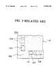
- FIGS. 1 and 2show the construction of a related semiconductor device having a flip-chip substrate 100 on which a semiconductor chip 102 is mounted in a face-down state respectively in an oblique view before the mounting of the semiconductor chip 102 and in a cross-sectional view after the mounting of the semiconductor chip 102.
- the substrate 100includes a base substrate 106 and a solder resist layer 110, wherein the base substrate 106 is formed of a commonly used printed circuit board and may include a plurality of interconnection layers. As indicated in the cross-sectional view of FIG. 2, the base substrate 106 carries a plurality of solder bumps 114 on a bottom surface thereof for external interconnection. Further, the base substrate 106 carries on a top surface thereof a conductor pattern 108, wherein the conductor pattern 108 is connected to a solder bump 114 by way of an interconnection pattern provided inside the base substrate 106.
- the solder resist layer 110is formed of an insulating resin and is provided on the base substrate 106 for preventing a short-circuit between the mounted semiconductor chip 102 and the conductor pattern 108.
- the solder resist layer 110is formed with four mutually isolated elongating slits 112 each exposing a part of the conductor pattern 108, wherein the elongating slits 112 are formed in correspondence to stud bumps 104 that are provided on a bottom surface of the semiconductor chip 102 along a peripheral edge thereof for external connection. It should be noted that the elongating slits 112 are isolated from each other by a corner part 122 of the solder resist layer 110.
- the stud bumps 104 protruding from the semiconductor chip 102are soldered upon the corresponding conductor pattern 108 by a solder alloy 116. Further, the space between the semiconductor chip 102 and the flip-chip substrate 100 is filled by an under-fill resin layer 118.
- the under-fill resin layer 118as such, the stress induced in the part where the stud bump 104 is soldered to the conductor pattern 108 as a result of the difference in the thermal expansion coefficient between the semiconductor chip 102 and the base substrate 106, is successfully relaxed and the interconnection between the stud bump 104 and the conductor pattern 108 is protected from a mechanical as well as electrical failure.
- the under-fill resin 118is introduced into the foregoing space between the semiconductor chip 102 and the flip-chip substrate 100 after the semiconductor chip 102 is soldered upon the conductor pattern 108 on the base substrate 106 by the solder alloy 116 as indicated in FIG. 3, wherein it can be seen that the under-fill resin 118 is caused to flow over the surface of the flip-chip substrate 100 in a molten state.
- the under-fill resin 118thus introduced is cured subsequently by applying a heat treatment process.
- the opening corresponding to the slit 112is formed for each of the stud bumps 104.
- the formation of such minute openings in the solder resist layer 122is difficult in view of the reduced pitch of 85-100 ⁇ m for the stud bumps 104.
- a void 120is tend to be formed in the under-fill resin layer 118 generally at the end part of the elongating slit 112 as indicated in FIG. 4.
- the voidmay be filled by the molten solder alloy 116 as a reflowing process of the solder alloy is conducted, while the solder alloy thus filling the void 120 may cause an unwanted short-circuit in the stud bump 104.
- the heating process applied for curing the under-fill resin layer 118may induce an expansion of the air filling the void 120.
- the under-fill resin layer 118is cracked in the vicinity of the void 120.
- the stud bump 104 and the conductor pattern 108may be disconnected due to the mechanical deformation associated with the expansion of the void 120.
- the formation of the void 120occurs primarily due to the difference in the flowing speed of the molten resin 118 over the solder resist layer 110 and over the base substrate 106 exposed by the elongating slit 112 including the conductor pattern 108.
- the flowing speed of the molten resin 118 over the solder resist layer 110is substantially larger than the flowing speed of the molten resin over the exposed surface of the slit 112 indicated in FIG. 3 by an arrow V 2 .
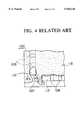
- FIG. 4shows the mechanism of formation of the void 120.
- the molten under-fill resin 118is supplied from the upper part in the plan view of FIG. 4 wherein the molten resin 118 thus introduced is caused to flow in the downward direction of the drawing.
- the molten resin 118flows over the flat solder resist layer 110 covering the surface of the base substrate 106 at the speed V 1 larger than the speed V 2 for the case the same molten resin flows over the exposed surface of the elongating slit 112.
- the direction of flow of the molten resin 118is bent at the edge part or end part of the slit 112 as indicated by arrows A in FIG.
- the molten resin 118goes around the edge part of the elongating slit 112.
- the isolated voids 120are formed at the edge part of the slits 112 as indicated in FIG. 5.
- the reason that the foregoing difference in the flowing speed arisesis considered as follows.
- the solder resist layer 110which is also formed of a resin
- an excellent wettingis guaranteed due to the affinity of the materials forming the molten under-fill resin layer 118 and the solder resist layer 110.
- the solder resist layer 110has a flat smooth surface that facilitates the smooth flow of the molten resin layer 118 over the solder resist layer 110.
- the molten resin 118When the molten under-fill resin layer 118 flows over the exposed surface of the elongating slit 112, on the other hand, the molten resin 118 encounters irregular projections formed by the conductor patterns 108, wherein the irregular projections act as an obstacle to the flow of the molten resin 108. Further, the elongating slit 112 defines a groove characterized by a stepped edge, while the existence of such a stepped edge increases the surface area and hence the friction against the flow of molten under-fill resin layer 118.
- void 120becomes conspicuous when the semiconductor chip 102 used in the semiconductor device has a size of 10 mm or more fore each edge.
- Another and more specific object of the present inventionis to provide a semiconductor device including a flip-chip substrate carrying thereon a semiconductor chip, wherein a resin layer fills a space between said flip-chip substrate and said semiconductor chip without forming a void.
- Another object of the present inventionis to provide a semiconductor device, comprising:
- said flip-chip substrateincluding a conductor pattern and an insulation film, such that said insulation film covers said conductor pattern;
- cutoutis provided in correspondence to said electrodes and extends continuously to form a closed loop.
- the resin layer filing the foregoing space between the semiconductor chip and the flip-chip substrateis formed without a substantial void by merely causing a molten resin from one side of the space to the opposite side.
- the cutoutis now formed in the continuous form without interruption, the flow of the molten resin going around the edge part of the cutout as explained with reference to FIG. 4 does not occur anymore, and the problem of the void remaining in the cured resist layer is successfully eliminated.
- FIG. 1is a diagram showing the construction of a conventional semiconductor device using a flip-chip substrate
- FIG. 2is a diagram showing the semiconductor device of FIG. 1 in a cross-sectional view
- FIGS. 3-5are diagrams showing a flow of a molten resin when forming the semiconductor device of FIG. 1;
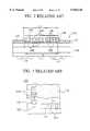
- FIG. 6is a diagram showing the construction of a semiconductor device using a flip-chip substrate according to a first embodiment of the present invention
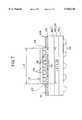
- FIG. 7is a diagram showing the semiconductor device of FIG. 6 in a cross-sectional view
- FIGS. 8-11are diagrams showing a flow of a molten resin when forming the semiconductor device of FIG. 6;
- FIG. 12is a diagram showing the construction of a semiconductor device using a flip-chip substrate according to a second embodiment of the present invention.
- FIG. 13is a diagram showing the construction of a semiconductor device using a flip-chip substrate according to a third embodiment of the present invention.
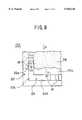
- FIG. 6shows the construction of the semiconductor device according to a first embodiment of the present invention in an exploded state while FIG. 7 shows the same semiconductor device in a cross-sectional view.
- the semiconductor deviceincludes a flip-chip substrate 10A and a semiconductor chip 12, wherein the flip-chip substrate 10A includes a base substrate 16 of a glass-epoxy or polycarbonate and a solder resist layer 20 is provided on the base substrate 16.
- the base substrate 16may have a multilayer structure including a plurality of layers 16a-16c each carrying a corresponding conductor pattern.
- a conductor pattern 18is formed on the top surface of the base substrate 16.
- bump electrodes 24are formed on a bottom surface of the base substrate 16 for external interconnection.
- the conductor pattern 18is connected to the solder bumps 24 by the conductor patterns formed inside the base layer 16.
- the conductor pattern 18 as well as the conductor patterns inside the base layer 16 including the layers 16a-16cmay be formed by a screen printing of a Cu pattern.
- the solder resist layer 20is typically formed of an insulation film of an epoxy resin and covers the top surface of the base substrate 16 with a generally uniform thickness, wherein the solder resist layer 20 is provided for avoiding a short-circuit between the semiconductor chip 12 and the conductor pattern 18.
- the solder resist layer 20is formed with a continuous cutout 22 extending along a periphery of the semiconductor chip 12 to be mounted on the base substrate 16.
- the semiconductor chip 12carries stud bumps 14 on a bottom surface thereof for electrical interconnection along the periphery thereof.
- the stud bumps 14achieve an electrical contact with corresponding parts of the conductor pattern 18.
- the continuous cutout 22 in the solder resist layer 20there is formed a central island 20a of the material identical in composition and thickness to the solder resist layer 20. The details and functions of the continuous cutout 22 will be described later in more detail.
- the stud bumps 14are formed of Au and provided conveniently by using the art of wire bonding process.
- solder alloy 26By soldering the stud bumps 14 to the corresponding conductor patterns 18 by a solder alloy 26 as indicated in the cross-sectional view of FIG. 7, the semiconductor chip 12 is mounted on the flip-chip substrate 10A electrically as well as mechanically in a face-down state.
- a solder alloy of the Sn--Ag system typically having a composition of Sn 96.5 wt % and Ag 3.5 wt %may be used for the solder alloy 26.
- the solder alloy 26may be pre-coated on the conductor pattern 18.
- FIG. 7shows an under-fill resin layer 28 provided between the semiconductor chip 12 and the flip-chip substrate 10A.
- the under-fill resin layer 28fills a space formed between the bottom surface of the chip 12 and the exposed top surface of the base substrate 16.
- the under-fill resin layer 28is applied in the low-viscosity molten state.
- a low viscosity epoxy resinis selected for the under-fill resin layer 28.
- the semiconductor deviceshows an improved reliability.
- the sameis cured by applying a heat treatment process.
- the continuous cutout 22is a region in which the solder resist layer 20 is selectively removed generally in a rectangular form along the peripheral edge of the semiconductor chip 12. Thereby, the surface of the base substrate 16 and the conductor pattern 18 are exposed at the bottom of the cutout 22.
- the four cutouts 112 of FIG. 1are interconnected with each other by removing the solder resist layer 20 at the four corners.
- the part of the cutout 22 extending in an X-direction, in which direction the molten resin forming the under-fill resin layer 28 is caused to flowis designated as a longitudinal part 22a, while the part extending in a Y-direction perpendicularly to the X-direction is designated as a lateral part 22b. Further, the part where a longitudinal part 22a continues to a lateral part 22b is designated as a corner part 22c. See FIG. 6.
- the rectangular cutout 22defines a rectangular central island 20a of the same material as the solder resist layer 20, wherein it should be noted that the central island 20a covers the conductor pattern 18 underneath, and the problem of the conductor pattern 18 contacting the bottom surface of the semiconductor chip 12, on which the semiconductor device patterns are formed, is successfully avoided.
- the central island 20ais not to be formed, it is therefore necessary to design the conductor pattern 18 so as to avoid the foregoing central part of the cutout 22.
- the degree of freedom of designing the conductor pattern 18is increased substantially.
- FIGS. 8-11show the result of the experiments conducted by the inventor, wherein those parts corresponding to the parts described heretofore are designated by the same reference numerals and the description thereof will be omitted.
- a molten resinis supplied to the space formed between the semiconductor chip 12 and the flip-chip substrate 10A and is caused to flow in the X-direction.
- the molten resin 28By continuously causing the molten resin 28 to flow in the X-direction further, the molten resin 28 covers the surface of the flip-chip substrate 10A as indicated in FIG. 11, without forming a void.
- the forgoing corner part 22c of the cutout 22functions to reduce the speed of the molten resin flowing over the island region 20a of the solder resin 20.
- FIG. 12shows the construction of a flip-chip substrate 10B according to a second embodiment of the present invention in an oblique view, wherein those parts corresponding to the parts described previously are designated by the same reference numerals and the description thereof will be omitted.
- the flip-chip substrate 10Bis used as a mother board of a multiple-chip module (MCM), wherein it should be noted that the flip-chip substrate 10B carries thereon a plurality of semiconductor chips 12. Thereby, the part of the solder resist layer 20 on which the semiconductor chip 12 is to be mounted is formed with the continuous cutout 22 that is formed along the periphery of the semiconductor chip 12.
- MCMmultiple-chip module
- the cutout 22defines the central island 20a, wherein the central island 20a of the present embodiment has a rough surface 30, which may typically be formed by a sand-blasting or an etching process.
- the molten resin flowing over the central island 20aexperiences an increased friction and the speed V 1 of the molten resist over the rough surface 30 is reduced.
- the rough surface 30thereby functions as a mechanism for matching the flow speed V 1 of the molten resin over the central island 20a and the flow speed V 2 of the molten resin over the longitudinal part 22a of the cutout 22.
- the present embodimentis also effective in avoiding the going-around of the molten resin when forming the under-fill resin layer 28, and the formation of the void or cavity therein is effectively avoided. It should be noted that the roughness of the foregoing surface 30 is controlled as desired by controlling the duration of the sandblasting process or an etching process.
- FIG. 13shows the construction of a flip-chip substrate 10C according to a third embodiment of the present invention, wherein those parts corresponding to the parts described previously are designated by the same reference numerals and the description thereof will be omitted.
- the flip-chip substrate 10Cforms an IC card 32 and carries a card-edge connector 34 on an edge part thereof.
- the semiconductor chip 12 mounted on the flip-chip substrate 10Cis fitted into the continuous cutout 22 formed in the solder resist layer 20 covering the base substrate 16.
- the gap formed between the semiconductor chip 12 and the flip-chip substrate 10Cis filled by the under-fill resin 28.
- the semiconductor chips 12are more or less buried in the solder resist layer 20, and the thickness of the IC card 32 is reduced successfully, without increasing the risk of short-circuit between the semiconductor chip 12 and the conductor pattern 18 formed on the base substrate 16 of the flip-chip substrate 10C.
Landscapes
- Engineering & Computer Science (AREA)
- Computer Hardware Design (AREA)
- Microelectronics & Electronic Packaging (AREA)
- Power Engineering (AREA)
- Physics & Mathematics (AREA)
- Condensed Matter Physics & Semiconductors (AREA)
- General Physics & Mathematics (AREA)
- Manufacturing & Machinery (AREA)
- Wire Bonding (AREA)
Abstract
Description
Claims (6)
Priority Applications (1)
| Application Number | Priority Date | Filing Date | Title |
|---|---|---|---|
| US09/162,770US5920126A (en) | 1997-10-02 | 1998-09-30 | Semiconductor device including a flip-chip substrate |
Applications Claiming Priority (4)
| Application Number | Priority Date | Filing Date | Title |
|---|---|---|---|
| JP9-270174 | 1997-10-02 | ||
| JP27017497AJPH11111894A (en) | 1997-10-02 | 1997-10-02 | Substrate for flip chip mounting |
| US3479998A | 1998-03-04 | 1998-03-04 | |
| US09/162,770US5920126A (en) | 1997-10-02 | 1998-09-30 | Semiconductor device including a flip-chip substrate |
Related Parent Applications (1)
| Application Number | Title | Priority Date | Filing Date |
|---|---|---|---|
| US3479998AContinuation-In-Part | 1997-10-02 | 1998-03-04 |
Publications (1)
| Publication Number | Publication Date |
|---|---|
| US5920126Atrue US5920126A (en) | 1999-07-06 |
Family
ID=26549098
Family Applications (1)
| Application Number | Title | Priority Date | Filing Date |
|---|---|---|---|
| US09/162,770Expired - LifetimeUS5920126A (en) | 1997-10-02 | 1998-09-30 | Semiconductor device including a flip-chip substrate |
Country Status (1)
| Country | Link |
|---|---|
| US (1) | US5920126A (en) |
Cited By (20)
| Publication number | Priority date | Publication date | Assignee | Title |
|---|---|---|---|---|
| US6133064A (en)* | 1999-05-27 | 2000-10-17 | Lsi Logic Corporation | Flip chip ball grid array package with laminated substrate |
| US6153939A (en)* | 1999-05-24 | 2000-11-28 | Advanced Semiconductor Engineering, Inc. | Flip-chip semiconductor device with enhanced reliability and manufacturing efficiency, and the method for under filling the same |
| US6217990B1 (en)* | 1997-05-07 | 2001-04-17 | Denso Corporation | Multilayer circuit board having no local warp on mounting surface thereof |
| US6597070B2 (en)* | 2000-02-01 | 2003-07-22 | Nec Electronics Corporation | Semiconductor device and method of manufacturing the same |
| US20050131509A1 (en)* | 2003-12-16 | 2005-06-16 | Liliana Atanassoska | Coatings for implantable electrodes |
| US20080029297A1 (en)* | 2006-08-01 | 2008-02-07 | Shinko Electric Industries Co., Ltd. | Wiring substrate and manufacturing method thereof, and semiconductor device |
| US20090097220A1 (en)* | 2007-10-16 | 2009-04-16 | Samsung Electro-Mechanics Co., Ltd. | Printed circuit board |
| US20100155965A1 (en)* | 2008-12-24 | 2010-06-24 | Shinko Electric Industries Co., Ltd. | Semiconductor device |
| US20110316162A1 (en)* | 2010-06-24 | 2011-12-29 | Ko Wonjun | Integrated circuit packaging system with trenches and method of manufacture thereof |
| US8089148B1 (en) | 2009-08-11 | 2012-01-03 | Amkor Technology, Inc. | Circuit board and semiconductor device having the same |
| US20130093072A1 (en)* | 2011-10-13 | 2013-04-18 | Stmicroelectronics Pte Ltd. | Leadframe pad design with enhanced robustness to die crack failure |
| CN103180943A (en)* | 2010-11-04 | 2013-06-26 | 阿尔卑斯电气株式会社 | Electronic component module |
| US8492893B1 (en) | 2011-03-16 | 2013-07-23 | Amkor Technology, Inc. | Semiconductor device capable of preventing dielectric layer from cracking |
| US8536458B1 (en) | 2009-03-30 | 2013-09-17 | Amkor Technology, Inc. | Fine pitch copper pillar package and method |
| US20150347893A1 (en)* | 2014-05-27 | 2015-12-03 | Kabushiki Kaisha Toshiba | Ic card substrate and fitted ic card |
| US20160056119A1 (en)* | 2014-08-20 | 2016-02-25 | Samsung Electro-Mechanics Co., Ltd. | Flip chip package and manufacturing method thereof |
| US9775992B2 (en) | 2015-02-13 | 2017-10-03 | Cardiac Pacemakers, Inc. | Implantable electrode |
| US11211300B2 (en) | 2017-01-31 | 2021-12-28 | Sony Semiconductor Solutions Corporation | Electronic component and camera module |
| US11282717B2 (en)* | 2018-03-30 | 2022-03-22 | Intel Corporation | Micro-electronic package with substrate protrusion to facilitate dispense of underfill between a narrow die-to-die gap |
| US11626336B2 (en)* | 2019-10-01 | 2023-04-11 | Qualcomm Incorporated | Package comprising a solder resist layer configured as a seating plane for a device |
Citations (5)
| Publication number | Priority date | Publication date | Assignee | Title |
|---|---|---|---|---|
| US5394490A (en)* | 1992-08-11 | 1995-02-28 | Hitachi, Ltd. | Semiconductor device having an optical waveguide interposed in the space between electrode members |
| JPH08181239A (en)* | 1994-12-22 | 1996-07-12 | Matsushita Electric Ind Co Ltd | Circuit board for flip chip mounting |
| US5751060A (en)* | 1995-01-25 | 1998-05-12 | International Business Machines Corporation | Electronic package |
| US5786230A (en)* | 1995-05-01 | 1998-07-28 | Motorola, Inc. | Method of fabricating multi-chip packages |
| US5844319A (en)* | 1997-03-03 | 1998-12-01 | Motorola Corporation | Microelectronic assembly with collar surrounding integrated circuit component on a substrate |
- 1998
- 1998-09-30USUS09/162,770patent/US5920126A/ennot_activeExpired - Lifetime
Patent Citations (5)
| Publication number | Priority date | Publication date | Assignee | Title |
|---|---|---|---|---|
| US5394490A (en)* | 1992-08-11 | 1995-02-28 | Hitachi, Ltd. | Semiconductor device having an optical waveguide interposed in the space between electrode members |
| JPH08181239A (en)* | 1994-12-22 | 1996-07-12 | Matsushita Electric Ind Co Ltd | Circuit board for flip chip mounting |
| US5751060A (en)* | 1995-01-25 | 1998-05-12 | International Business Machines Corporation | Electronic package |
| US5786230A (en)* | 1995-05-01 | 1998-07-28 | Motorola, Inc. | Method of fabricating multi-chip packages |
| US5844319A (en)* | 1997-03-03 | 1998-12-01 | Motorola Corporation | Microelectronic assembly with collar surrounding integrated circuit component on a substrate |
Cited By (35)
| Publication number | Priority date | Publication date | Assignee | Title |
|---|---|---|---|---|
| US6217990B1 (en)* | 1997-05-07 | 2001-04-17 | Denso Corporation | Multilayer circuit board having no local warp on mounting surface thereof |
| US6153939A (en)* | 1999-05-24 | 2000-11-28 | Advanced Semiconductor Engineering, Inc. | Flip-chip semiconductor device with enhanced reliability and manufacturing efficiency, and the method for under filling the same |
| US6133064A (en)* | 1999-05-27 | 2000-10-17 | Lsi Logic Corporation | Flip chip ball grid array package with laminated substrate |
| US6597070B2 (en)* | 2000-02-01 | 2003-07-22 | Nec Electronics Corporation | Semiconductor device and method of manufacturing the same |
| US8017178B2 (en)* | 2003-12-16 | 2011-09-13 | Cardiac Pacemakers, Inc. | Coatings for implantable electrodes |
| US20060035026A1 (en)* | 2003-12-16 | 2006-02-16 | Cardiac Pacemakers, Inc. | Coatings for implantable electrodes |
| US8017179B2 (en) | 2003-12-16 | 2011-09-13 | Cardiac Pacemakers, Inc. | Coatings for implantable electrodes |
| US20050131509A1 (en)* | 2003-12-16 | 2005-06-16 | Liliana Atanassoska | Coatings for implantable electrodes |
| US20080029297A1 (en)* | 2006-08-01 | 2008-02-07 | Shinko Electric Industries Co., Ltd. | Wiring substrate and manufacturing method thereof, and semiconductor device |
| US7943863B2 (en) | 2006-08-01 | 2011-05-17 | Shinko Electric Industries Co., Ltd. | Wiring substrate and manufacturing method thereof, and semiconductor device |
| US20090097220A1 (en)* | 2007-10-16 | 2009-04-16 | Samsung Electro-Mechanics Co., Ltd. | Printed circuit board |
| US8169083B2 (en)* | 2008-12-24 | 2012-05-01 | Shinko Electric Industries Co., Ltd. | Semiconductor device |
| US20100155965A1 (en)* | 2008-12-24 | 2010-06-24 | Shinko Electric Industries Co., Ltd. | Semiconductor device |
| US11088064B2 (en) | 2009-03-30 | 2021-08-10 | Amkor Technology Singapore Holding Pte. Ltd. | Fine pitch copper pillar package and method |
| US12191241B2 (en) | 2009-03-30 | 2025-01-07 | Amkor Technology Singapore Holding Pte. Ltd. | Fine pitch copper pillar package and method |
| US9462690B1 (en) | 2009-03-30 | 2016-10-04 | Amkor Technologies, Inc. | Fine pitch copper pillar package and method |
| US8536458B1 (en) | 2009-03-30 | 2013-09-17 | Amkor Technology, Inc. | Fine pitch copper pillar package and method |
| US10418318B1 (en) | 2009-03-30 | 2019-09-17 | Amkor Technology, Inc. | Fine pitch copper pillar package and method |
| US10224270B1 (en) | 2009-03-30 | 2019-03-05 | Amkor Technology, Inc. | Fine pitch copper pillar package and method |
| US8089148B1 (en) | 2009-08-11 | 2012-01-03 | Amkor Technology, Inc. | Circuit board and semiconductor device having the same |
| US20110316162A1 (en)* | 2010-06-24 | 2011-12-29 | Ko Wonjun | Integrated circuit packaging system with trenches and method of manufacture thereof |
| US8536718B2 (en)* | 2010-06-24 | 2013-09-17 | Stats Chippac Ltd. | Integrated circuit packaging system with trenches and method of manufacture thereof |
| CN103180943A (en)* | 2010-11-04 | 2013-06-26 | 阿尔卑斯电气株式会社 | Electronic component module |
| CN103180943B (en)* | 2010-11-04 | 2016-04-13 | 阿尔卑斯电气株式会社 | Electronic component module |
| US8492893B1 (en) | 2011-03-16 | 2013-07-23 | Amkor Technology, Inc. | Semiconductor device capable of preventing dielectric layer from cracking |
| US20130093072A1 (en)* | 2011-10-13 | 2013-04-18 | Stmicroelectronics Pte Ltd. | Leadframe pad design with enhanced robustness to die crack failure |
| US9600757B2 (en)* | 2014-05-27 | 2017-03-21 | Kabushiki Kaisha Toshiba | IC card substrate and fitted IC card |
| US20150347893A1 (en)* | 2014-05-27 | 2015-12-03 | Kabushiki Kaisha Toshiba | Ic card substrate and fitted ic card |
| US9583368B2 (en) | 2014-08-20 | 2017-02-28 | Samsung Electro-Mechanics Co., Ltd. | Flip chip package and manufacturing method thereof |
| US20160056119A1 (en)* | 2014-08-20 | 2016-02-25 | Samsung Electro-Mechanics Co., Ltd. | Flip chip package and manufacturing method thereof |
| US9775992B2 (en) | 2015-02-13 | 2017-10-03 | Cardiac Pacemakers, Inc. | Implantable electrode |
| US11211300B2 (en) | 2017-01-31 | 2021-12-28 | Sony Semiconductor Solutions Corporation | Electronic component and camera module |
| US11282717B2 (en)* | 2018-03-30 | 2022-03-22 | Intel Corporation | Micro-electronic package with substrate protrusion to facilitate dispense of underfill between a narrow die-to-die gap |
| US11776821B2 (en) | 2018-03-30 | 2023-10-03 | Intel Corporation | Micro-electronic package with substrate protrusion to facilitate dispense of underfill between a narrow die-to-die gap |
| US11626336B2 (en)* | 2019-10-01 | 2023-04-11 | Qualcomm Incorporated | Package comprising a solder resist layer configured as a seating plane for a device |
Similar Documents
| Publication | Publication Date | Title |
|---|---|---|
| US5920126A (en) | Semiconductor device including a flip-chip substrate | |
| KR100448952B1 (en) | Semiconductor module | |
| US6525414B2 (en) | Semiconductor device including a wiring board and semiconductor elements mounted thereon | |
| US6049122A (en) | Flip chip mounting substrate with resin filled between substrate and semiconductor chip | |
| JP3973340B2 (en) | Semiconductor device, wiring board, and manufacturing method thereof | |
| US6252298B1 (en) | Semiconductor chip package using flexible circuit board with central opening | |
| KR100694739B1 (en) | Ball grid array package with multiple power / ground planes | |
| US6229711B1 (en) | Flip-chip mount board and flip-chip mount structure with improved mounting reliability | |
| US5578525A (en) | Semiconductor device and a fabrication process thereof | |
| US6518666B1 (en) | Circuit board reducing a warp and a method of mounting an integrated circuit chip | |
| US5760469A (en) | Semiconductor device and semiconductor device mounting board | |
| US8378482B2 (en) | Wiring board | |
| KR100449307B1 (en) | Semiconductor device and method for manufacturing the same | |
| US9318460B2 (en) | Substrate and assembly thereof with dielectric removal for increased post height | |
| KR20090126762A (en) | Printed circuit board mounted with semiconductor chip and manufacturing method | |
| JPH10233463A (en) | Semiconductor device and manufacturing method thereof | |
| US20250125269A1 (en) | Circuit board | |
| US20240381530A1 (en) | Circuit board and semiconductor package comprising same | |
| US20040164429A1 (en) | Chip carrier film, method of manufacturing the chip carrier film and liquid crystal display using the chip carrier film | |
| US6492715B1 (en) | Integrated semiconductor package | |
| US11862608B2 (en) | Semiconductor package | |
| JPH11111894A (en) | Substrate for flip chip mounting | |
| JP2002208657A (en) | Semiconductor device and semiconductor device mounting substrate | |
| US20250192021A1 (en) | Semiconductor package | |
| KR100197877B1 (en) | PCB Board Structure of BGA Semiconductor Package |
Legal Events
| Date | Code | Title | Description |
|---|---|---|---|
| AS | Assignment | Owner name:FUJITSU LIMITED, JAPAN Free format text:ASSIGNMENT OF ASSIGNORS INTEREST;ASSIGNOR:SOHARA, TSUYOSHI;REEL/FRAME:009826/0103 Effective date:19980924 | |
| STCF | Information on status: patent grant | Free format text:PATENTED CASE | |
| FEPP | Fee payment procedure | Free format text:PAYOR NUMBER ASSIGNED (ORIGINAL EVENT CODE: ASPN); ENTITY STATUS OF PATENT OWNER: LARGE ENTITY | |
| AS | Assignment | Owner name:FUJITSU LIMITED, JAPAN Free format text:(ASSIGNMENT OF ASSIGNOR'S INTEREST) RECORD TO CORRECT THE EXECUTION DATE ON A DOCUMENT PREVIOUSLY RECORDED AT REEL/9826, FRAME/0103;ASSIGNOR:SOHARA, TSUYOSHI;REEL/FRAME:010418/0553 Effective date:19990225 | |
| AS | Assignment | Owner name:SHINKO ELECTRIC INDUSTRIES, CO., LTD., JAPAN Free format text:ASSIGNMENT OF ASSIGNORS INTEREST;ASSIGNOR:FUJITSU LIMITED;REEL/FRAME:010949/0078 Effective date:20000628 | |
| FPAY | Fee payment | Year of fee payment:4 | |
| FPAY | Fee payment | Year of fee payment:8 | |
| FPAY | Fee payment | Year of fee payment:12 |