US5920123A - Multichip module assembly having via contacts and method of making the same - Google Patents
Multichip module assembly having via contacts and method of making the sameDownload PDFInfo
- Publication number
- US5920123A US5920123AUS08/788,004US78800497AUS5920123AUS 5920123 AUS5920123 AUS 5920123AUS 78800497 AUS78800497 AUS 78800497AUS 5920123 AUS5920123 AUS 5920123A
- Authority
- US
- United States
- Prior art keywords
- integrated circuit
- vias
- conductive
- group
- circuit board
- Prior art date
- Legal status (The legal status is an assumption and is not a legal conclusion. Google has not performed a legal analysis and makes no representation as to the accuracy of the status listed.)
- Expired - Lifetime
Links
- 238000004519manufacturing processMethods0.000titledescription2
- 239000004020conductorSubstances0.000claimsabstractdescription25
- 239000000463materialSubstances0.000claimsabstractdescription17
- 239000000853adhesiveSubstances0.000claimsabstractdescription10
- 230000001070adhesive effectEffects0.000claimsabstractdescription10
- 238000000034methodMethods0.000claimsdescription26
- 239000000758substrateSubstances0.000claimsdescription13
- 239000012790adhesive layerSubstances0.000claimsdescription12
- 239000004593EpoxySubstances0.000claimsdescription8
- 239000010410layerSubstances0.000claimsdescription8
- 229910000679solderInorganic materials0.000claimsdescription7
- 238000004891communicationMethods0.000claimsdescription6
- 238000007747platingMethods0.000description3
- 230000000712assemblyEffects0.000description2
- 238000000429assemblyMethods0.000description2
- 238000005476solderingMethods0.000description2
- 230000008646thermal stressEffects0.000description2
- RYGMFSIKBFXOCR-UHFFFAOYSA-NCopperChemical compound[Cu]RYGMFSIKBFXOCR-UHFFFAOYSA-N0.000description1
- 239000004642PolyimideSubstances0.000description1
- XAGFODPZIPBFFR-UHFFFAOYSA-NaluminiumChemical compound[Al]XAGFODPZIPBFFR-UHFFFAOYSA-N0.000description1
- 229910052782aluminiumInorganic materials0.000description1
- 230000005540biological transmissionEffects0.000description1
- 239000000969carrierSubstances0.000description1
- 229910010293ceramic materialInorganic materials0.000description1
- 238000010276constructionMethods0.000description1
- 229910052802copperInorganic materials0.000description1
- 239000010949copperSubstances0.000description1
- 230000001419dependent effectEffects0.000description1
- 238000000151depositionMethods0.000description1
- 238000005553drillingMethods0.000description1
- -1e.g.Substances0.000description1
- 238000009713electroplatingMethods0.000description1
- 230000007613environmental effectEffects0.000description1
- 238000005530etchingMethods0.000description1
- 238000005429filling processMethods0.000description1
- 238000002844meltingMethods0.000description1
- 230000008018meltingEffects0.000description1
- 238000004806packaging method and processMethods0.000description1
- 238000003909pattern recognitionMethods0.000description1
- 229920001721polyimidePolymers0.000description1
- 230000035882stressEffects0.000description1
- 238000005382thermal cyclingMethods0.000description1
- 229920001169thermoplasticPolymers0.000description1
- 229920001187thermosetting polymerPolymers0.000description1
- 239000004416thermosoftening plasticSubstances0.000description1
Images

Classifications
- H—ELECTRICITY
- H01—ELECTRIC ELEMENTS
- H01L—SEMICONDUCTOR DEVICES NOT COVERED BY CLASS H10
- H01L24/00—Arrangements for connecting or disconnecting semiconductor or solid-state bodies; Methods or apparatus related thereto
- H01L24/80—Methods for connecting semiconductor or other solid state bodies using means for bonding being attached to, or being formed on, the surface to be connected
- H01L24/83—Methods for connecting semiconductor or other solid state bodies using means for bonding being attached to, or being formed on, the surface to be connected using a layer connector
- H—ELECTRICITY
- H01—ELECTRIC ELEMENTS
- H01L—SEMICONDUCTOR DEVICES NOT COVERED BY CLASS H10
- H01L23/00—Details of semiconductor or other solid state devices
- H01L23/48—Arrangements for conducting electric current to or from the solid state body in operation, e.g. leads, terminal arrangements ; Selection of materials therefor
- H01L23/481—Internal lead connections, e.g. via connections, feedthrough structures
- H—ELECTRICITY
- H01—ELECTRIC ELEMENTS
- H01L—SEMICONDUCTOR DEVICES NOT COVERED BY CLASS H10
- H01L24/00—Arrangements for connecting or disconnecting semiconductor or solid-state bodies; Methods or apparatus related thereto
- H01L24/01—Means for bonding being attached to, or being formed on, the surface to be connected, e.g. chip-to-package, die-attach, "first-level" interconnects; Manufacturing methods related thereto
- H01L24/26—Layer connectors, e.g. plate connectors, solder or adhesive layers; Manufacturing methods related thereto
- H01L24/28—Structure, shape, material or disposition of the layer connectors prior to the connecting process
- H01L24/29—Structure, shape, material or disposition of the layer connectors prior to the connecting process of an individual layer connector
- H—ELECTRICITY
- H01—ELECTRIC ELEMENTS
- H01L—SEMICONDUCTOR DEVICES NOT COVERED BY CLASS H10
- H01L24/00—Arrangements for connecting or disconnecting semiconductor or solid-state bodies; Methods or apparatus related thereto
- H01L24/80—Methods for connecting semiconductor or other solid state bodies using means for bonding being attached to, or being formed on, the surface to be connected
- H01L24/81—Methods for connecting semiconductor or other solid state bodies using means for bonding being attached to, or being formed on, the surface to be connected using a bump connector
- H—ELECTRICITY
- H01—ELECTRIC ELEMENTS
- H01L—SEMICONDUCTOR DEVICES NOT COVERED BY CLASS H10
- H01L2224/00—Indexing scheme for arrangements for connecting or disconnecting semiconductor or solid-state bodies and methods related thereto as covered by H01L24/00
- H01L2224/01—Means for bonding being attached to, or being formed on, the surface to be connected, e.g. chip-to-package, die-attach, "first-level" interconnects; Manufacturing methods related thereto
- H01L2224/26—Layer connectors, e.g. plate connectors, solder or adhesive layers; Manufacturing methods related thereto
- H01L2224/28—Structure, shape, material or disposition of the layer connectors prior to the connecting process
- H01L2224/29—Structure, shape, material or disposition of the layer connectors prior to the connecting process of an individual layer connector
- H01L2224/29001—Core members of the layer connector
- H01L2224/29099—Material
- H01L2224/2919—Material with a principal constituent of the material being a polymer, e.g. polyester, phenolic based polymer, epoxy
- H—ELECTRICITY
- H01—ELECTRIC ELEMENTS
- H01L—SEMICONDUCTOR DEVICES NOT COVERED BY CLASS H10
- H01L2224/00—Indexing scheme for arrangements for connecting or disconnecting semiconductor or solid-state bodies and methods related thereto as covered by H01L24/00
- H01L2224/80—Methods for connecting semiconductor or other solid state bodies using means for bonding being attached to, or being formed on, the surface to be connected
- H01L2224/81—Methods for connecting semiconductor or other solid state bodies using means for bonding being attached to, or being formed on, the surface to be connected using a bump connector
- H01L2224/818—Bonding techniques
- H01L2224/81801—Soldering or alloying
- H—ELECTRICITY
- H01—ELECTRIC ELEMENTS
- H01L—SEMICONDUCTOR DEVICES NOT COVERED BY CLASS H10
- H01L2224/00—Indexing scheme for arrangements for connecting or disconnecting semiconductor or solid-state bodies and methods related thereto as covered by H01L24/00
- H01L2224/80—Methods for connecting semiconductor or other solid state bodies using means for bonding being attached to, or being formed on, the surface to be connected
- H01L2224/83—Methods for connecting semiconductor or other solid state bodies using means for bonding being attached to, or being formed on, the surface to be connected using a layer connector
- H01L2224/8319—Arrangement of the layer connectors prior to mounting
- H—ELECTRICITY
- H01—ELECTRIC ELEMENTS
- H01L—SEMICONDUCTOR DEVICES NOT COVERED BY CLASS H10
- H01L2224/00—Indexing scheme for arrangements for connecting or disconnecting semiconductor or solid-state bodies and methods related thereto as covered by H01L24/00
- H01L2224/80—Methods for connecting semiconductor or other solid state bodies using means for bonding being attached to, or being formed on, the surface to be connected
- H01L2224/83—Methods for connecting semiconductor or other solid state bodies using means for bonding being attached to, or being formed on, the surface to be connected using a layer connector
- H01L2224/838—Bonding techniques
- H01L2224/8385—Bonding techniques using a polymer adhesive, e.g. an adhesive based on silicone, epoxy, polyimide, polyester
- H—ELECTRICITY
- H01—ELECTRIC ELEMENTS
- H01L—SEMICONDUCTOR DEVICES NOT COVERED BY CLASS H10
- H01L2924/00—Indexing scheme for arrangements or methods for connecting or disconnecting semiconductor or solid-state bodies as covered by H01L24/00
- H01L2924/01—Chemical elements
- H01L2924/01005—Boron [B]
- H—ELECTRICITY
- H01—ELECTRIC ELEMENTS
- H01L—SEMICONDUCTOR DEVICES NOT COVERED BY CLASS H10
- H01L2924/00—Indexing scheme for arrangements or methods for connecting or disconnecting semiconductor or solid-state bodies as covered by H01L24/00
- H01L2924/01—Chemical elements
- H01L2924/01006—Carbon [C]
- H—ELECTRICITY
- H01—ELECTRIC ELEMENTS
- H01L—SEMICONDUCTOR DEVICES NOT COVERED BY CLASS H10
- H01L2924/00—Indexing scheme for arrangements or methods for connecting or disconnecting semiconductor or solid-state bodies as covered by H01L24/00
- H01L2924/01—Chemical elements
- H01L2924/01013—Aluminum [Al]
- H—ELECTRICITY
- H01—ELECTRIC ELEMENTS
- H01L—SEMICONDUCTOR DEVICES NOT COVERED BY CLASS H10
- H01L2924/00—Indexing scheme for arrangements or methods for connecting or disconnecting semiconductor or solid-state bodies as covered by H01L24/00
- H01L2924/01—Chemical elements
- H01L2924/01023—Vanadium [V]
- H—ELECTRICITY
- H01—ELECTRIC ELEMENTS
- H01L—SEMICONDUCTOR DEVICES NOT COVERED BY CLASS H10
- H01L2924/00—Indexing scheme for arrangements or methods for connecting or disconnecting semiconductor or solid-state bodies as covered by H01L24/00
- H01L2924/01—Chemical elements
- H01L2924/01027—Cobalt [Co]
- H—ELECTRICITY
- H01—ELECTRIC ELEMENTS
- H01L—SEMICONDUCTOR DEVICES NOT COVERED BY CLASS H10
- H01L2924/00—Indexing scheme for arrangements or methods for connecting or disconnecting semiconductor or solid-state bodies as covered by H01L24/00
- H01L2924/01—Chemical elements
- H01L2924/01029—Copper [Cu]
- H—ELECTRICITY
- H01—ELECTRIC ELEMENTS
- H01L—SEMICONDUCTOR DEVICES NOT COVERED BY CLASS H10
- H01L2924/00—Indexing scheme for arrangements or methods for connecting or disconnecting semiconductor or solid-state bodies as covered by H01L24/00
- H01L2924/01—Chemical elements
- H01L2924/01033—Arsenic [As]
- H—ELECTRICITY
- H01—ELECTRIC ELEMENTS
- H01L—SEMICONDUCTOR DEVICES NOT COVERED BY CLASS H10
- H01L2924/00—Indexing scheme for arrangements or methods for connecting or disconnecting semiconductor or solid-state bodies as covered by H01L24/00
- H01L2924/01—Chemical elements
- H01L2924/01078—Platinum [Pt]
- H—ELECTRICITY
- H01—ELECTRIC ELEMENTS
- H01L—SEMICONDUCTOR DEVICES NOT COVERED BY CLASS H10
- H01L2924/00—Indexing scheme for arrangements or methods for connecting or disconnecting semiconductor or solid-state bodies as covered by H01L24/00
- H01L2924/01—Chemical elements
- H01L2924/01082—Lead [Pb]
- H—ELECTRICITY
- H01—ELECTRIC ELEMENTS
- H01L—SEMICONDUCTOR DEVICES NOT COVERED BY CLASS H10
- H01L2924/00—Indexing scheme for arrangements or methods for connecting or disconnecting semiconductor or solid-state bodies as covered by H01L24/00
- H01L2924/013—Alloys
- H01L2924/014—Solder alloys
- H—ELECTRICITY
- H01—ELECTRIC ELEMENTS
- H01L—SEMICONDUCTOR DEVICES NOT COVERED BY CLASS H10
- H01L2924/00—Indexing scheme for arrangements or methods for connecting or disconnecting semiconductor or solid-state bodies as covered by H01L24/00
- H01L2924/06—Polymers
- H01L2924/0665—Epoxy resin
- H—ELECTRICITY
- H01—ELECTRIC ELEMENTS
- H01L—SEMICONDUCTOR DEVICES NOT COVERED BY CLASS H10
- H01L2924/00—Indexing scheme for arrangements or methods for connecting or disconnecting semiconductor or solid-state bodies as covered by H01L24/00
- H01L2924/06—Polymers
- H01L2924/078—Adhesive characteristics other than chemical
- H01L2924/07802—Adhesive characteristics other than chemical not being an ohmic electrical conductor
- H—ELECTRICITY
- H01—ELECTRIC ELEMENTS
- H01L—SEMICONDUCTOR DEVICES NOT COVERED BY CLASS H10
- H01L2924/00—Indexing scheme for arrangements or methods for connecting or disconnecting semiconductor or solid-state bodies as covered by H01L24/00
- H01L2924/10—Details of semiconductor or other solid state devices to be connected
- H01L2924/11—Device type
- H01L2924/12—Passive devices, e.g. 2 terminal devices
- H01L2924/1204—Optical Diode
- H01L2924/12042—LASER
- H—ELECTRICITY
- H01—ELECTRIC ELEMENTS
- H01L—SEMICONDUCTOR DEVICES NOT COVERED BY CLASS H10
- H01L2924/00—Indexing scheme for arrangements or methods for connecting or disconnecting semiconductor or solid-state bodies as covered by H01L24/00
- H01L2924/10—Details of semiconductor or other solid state devices to be connected
- H01L2924/11—Device type
- H01L2924/14—Integrated circuits
- H—ELECTRICITY
- H01—ELECTRIC ELEMENTS
- H01L—SEMICONDUCTOR DEVICES NOT COVERED BY CLASS H10
- H01L2924/00—Indexing scheme for arrangements or methods for connecting or disconnecting semiconductor or solid-state bodies as covered by H01L24/00
- H01L2924/30—Technical effects
- H01L2924/35—Mechanical effects
- H01L2924/351—Thermal stress
- Y—GENERAL TAGGING OF NEW TECHNOLOGICAL DEVELOPMENTS; GENERAL TAGGING OF CROSS-SECTIONAL TECHNOLOGIES SPANNING OVER SEVERAL SECTIONS OF THE IPC; TECHNICAL SUBJECTS COVERED BY FORMER USPC CROSS-REFERENCE ART COLLECTIONS [XRACs] AND DIGESTS
- Y10—TECHNICAL SUBJECTS COVERED BY FORMER USPC
- Y10T—TECHNICAL SUBJECTS COVERED BY FORMER US CLASSIFICATION
- Y10T29/00—Metal working
- Y10T29/49—Method of mechanical manufacture
- Y10T29/49002—Electrical device making
- Y10T29/49117—Conductor or circuit manufacturing
- Y10T29/49124—On flat or curved insulated base, e.g., printed circuit, etc.
- Y10T29/4913—Assembling to base an electrical component, e.g., capacitor, etc.
Definitions
- the present inventionrelates in general to the field of integrated circuits and in particular to an assembly on which multiple integrated circuits may be mounted.
- COBchip-on-board
- PCBprinted circuit board
- C4control-collapse-chip-connection
- the chipis connected to the PCB by interposing a plurality of interconnect bumps between the bond pads on the chip and a series of corresponding bump pads on the upper surface of the PCB.
- the PCBincludes plated through holes that connect the bottom bump pads to the top bump pads.
- an integrated circuit carrier assemblyfor holding an integrated circuit having a bond pad.
- the assemblyincludes a substrate that has a first side and a second opposing side.
- the substratehas a conductive trace coupled thereto and an opening formed therein.
- a conductive plateis disposed in the opening and is in electrical communication with the trace.
- a conductive contactis disposed in the opening and is in electrical communication with the conductive plate.
- An insulative adhesive layeris coupled to the substrate and an integrated circuit coupled to the insulative adhesive layer such that said bond pad is in electrical communication with the conductive contact.
- a multichip module assemblyincludes a printed circuit board onto which traces of electrically conductive material are formed and into which groups of plated vias are formed. Each group of vias being is associated with an integrated circuit to be mounted in the assembly and has a spacing pattern identical to the spacing pattern of the bond pads of the integrated circuit with which it is associated.
- a layer of insulative adhesive materialis provided, one side of which is attached to the printed circuit board.
- a plurality of integrated circuitsare attached to the other side of the adhesive material. Each integrated circuit has a plurality of bond pads in a spacing pattern.
- a conductive contactis disposed in each via to connect a bond pad to that via.
- a method of forming an assembly containing plurality of integrated circuitsincludes the steps of forming a plurality of groups of plated vias in a printed circuit board wherein each group of vias is associated with one of the integrated circuits in the assembly and the spacing pattern of the vias in each group corresponds to the spacing pattern of the bond pads on the integrated circuit with which said group of vias is associated.
- a plurality of traces of electrically conductive materialare formed on the printed circuit board.
- a layer of insulative adhesive materialis attached to one side of the printed circuit board.
- Each integrated circuitis attached to said insulative material such that the bond pads of the integrated circuit are aligned with the group of vias for that integrated circuit.
- Each viais filled with a conductive contact.
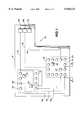
- FIG. 1is a top view of a multichip module assembly in accordance with the present invention.
- FIG. 2is a cross-sectional view of a portion of the multichip module assembly of FIG. 1 taken at section 2--2.
- the module assembly 10includes a substrate 12 which may be in the form of a printed circuit board 12.
- the material from which the printed circuit board 12 is fabricatedis a matter of design choice, depending on cost and environmental factors, and the printed circuit board 12 may for example be fabricated of FR4, polyimide or ceramic material.
- FIG. 1While the multichip module assembly 10 as illustrated in FIG. 1 is designed to accommodate two integrated circuits or "chips" 16 and 18, it will be apparent that an assembly in accordance with the present invention may be designed to accommodate any number of integrated circuits.
- the dotted line that is used to designate the integrated circuits 16, 18indicates that the integrated circuits are mounted on the underside of the printed circuit board 12.
- two groups of openings or vias 24 and 25are formed in printed circuit board 12.
- the group of vias designated 24is associated with integrated circuit 16, while the group of vias designated 25 is associated with integrated circuit 18.
- the spacing and pattern of vias 24correspond to the spacing and pattern of the bond pads on integrated circuit 16, while the spacing and pattern of vias 25 correspond to the spacing and pattern of the bond pads on integrated circuit 18.
- alignment holes 20, 22are formed in printed circuit board 12 for proper registering of integrated circuits 16 and 18, respectively, when the integrated circuits are installed as described below.
- the groups of vias 24 and 25 and the alignment holes 20 and 22may be formed by conventional mechanical or laser drilling techniques.
- printed circuit board 12initially has a layer of electrically conductive material, e.g., copper or aluminum, disposed on it. Circuitization of this electrically conductive material will be dependent on the functions to be performed by the integrated circuits in assembly 10. Unwanted conductive material is removed by well-known processes, e.g., etching, to produce the desired circuitization. In FIG. 1, for example, the result of this circuitization process produces a plurality of traces of conductive material 14a-14f and output pads 15a-15c. The traces 14a, 14c, 14d and 14f are formed on the top side of printed circuit board 12, while the traces 14b and 14e are formed on the underside of printed circuit board 12.
- electrically conductive materiale.g., copper or aluminum
- the printed circuit board 12may initially not contain any layer of conductive material and that the traces may be formed by plating or otherwise depositing conductor lines onto printed circuit board 12.
- all vias 24 and 25are thru-plated with an electrically conductive material to form plates 26 that have exterior surfaces that conform to the interior surfaces of the vias 24 and 25.
- a plating mask(not shown) is first placed over the printed circuit board 12, leaving the vias 24 and 25 exposed.
- the vias 24 and 25are then plated using a conventional plating process, such as, for example, dip electroplating.
- the conductive material that is used to form the plates 26 in the vias 24 and 25is preferably the same electrically conductive material used to form the traces 14a-f.
- the area of the plated vias 24, 25should be less than or equal to the size of the bond pads on their respective associated integrated circuits.
- An insulative adhesive layer 27is then applied to the underside of printed circuit board 12 in those areas where the integrated circuits 16 and 18 will be mounted as shown in FIG. 2.
- a stencil(not shown) is applied to the printed circuit board 12 to cover the vias 24 and 25 and the alignment holes 20 and 22 and leave exposed those areas on the printed circuit board 12 where the integrated circuits 16 and 18 will be mounted.
- the stencilis removed.
- the adhesive layer 27may be made of a thermoplastic, thermoset or pressure sensitive material suitable for multichip module packaging applications and should be 2 mils or more in thickness to compensate for warping and wet out of the integrated circuit.
- the adhesive layer 27is the primary mechanism by which each integrated circuit 16 and 18 is mechanically connected to the assembly. Because the adhesive layer 27 is applied before the integrated circuits 16 and 18 are mounted, traces may be applied to both the upper and lower surfaces of the printed circuit board 12 as shown in FIG. 2, without risk of short circuits.
- Each integrated circuit 16, 18is mounted to the insulative adhesive layer 27.
- the following description of the mounting and via filling processes for the integrated circuit 16applies to all such integrated circuits.
- the bonding pads 28 of the integrated circuit 16are first aligned with the corresponding vias 24 on the printed circuit board 12 using the alignment holes 20 as guides.
- the integrated circuit 16is then laid on the adhesive layer 27 as shown in FIG. 2.
- the entire alignment and mounting operationmay be carried out on a conventional single-camera die attachment machine equipped with a pattern recognition system.
- the alignment and mounting operation in accordance with the present inventionrequires a single camera alignment system.
- the vias 24are then filled with conductive contacts 30 to provide an electrical connection between the bond pads 28 of the integrated circuit 16, the plated vias 24 the traces 14f and 14b as shown in FIG. 2.
- the contacts 30are formed from a conductive material, such as a conductive epoxy or a low melting temperature solder. If composed of conductive epoxy, the conductive contacts 30 are formed by conventional stencil printing or syringe dispensing techniques, and cured using the curing protocol recommended by the epoxy manufacturer. If solder is used, the conductive contacts 30 are formed by inverting the assembly shown in FIG. 2 and passing it through a wave soldering machine, such as those manufactured by Hollis Co. Prior to application of the conductive contacts 30, a stencil (not shown) is applied to the assembly 10 to expose the vias 24 and 25 while covering the remainder of the assembly 10. The stencil is removed after the soldering process.
- a conductive materialsuch as a conductive epoxy or a low melting temperature solder. If composed of conductive epoxy, the conductive contacts 30 are formed by conventional
- the interface between the generally cylindrical exterior surface of the contacts 30, the interior surface areas of the plates 26, and the interior surfaces of the vias 24 and 25provide a greater surface area for the transport of heat away from and for the transmission of current to and from the integrated circuits 16 and 18 than is possible with conventional bump pads.
Landscapes
- Engineering & Computer Science (AREA)
- Computer Hardware Design (AREA)
- Microelectronics & Electronic Packaging (AREA)
- Power Engineering (AREA)
- Physics & Mathematics (AREA)
- Condensed Matter Physics & Semiconductors (AREA)
- General Physics & Mathematics (AREA)
- Wire Bonding (AREA)
Abstract
Description
Claims (17)
Priority Applications (1)
| Application Number | Priority Date | Filing Date | Title |
|---|---|---|---|
| US08/788,004US5920123A (en) | 1997-01-24 | 1997-01-24 | Multichip module assembly having via contacts and method of making the same |
Applications Claiming Priority (1)
| Application Number | Priority Date | Filing Date | Title |
|---|---|---|---|
| US08/788,004US5920123A (en) | 1997-01-24 | 1997-01-24 | Multichip module assembly having via contacts and method of making the same |
Publications (1)
| Publication Number | Publication Date |
|---|---|
| US5920123Atrue US5920123A (en) | 1999-07-06 |
Family
ID=25143147
Family Applications (1)
| Application Number | Title | Priority Date | Filing Date |
|---|---|---|---|
| US08/788,004Expired - LifetimeUS5920123A (en) | 1997-01-24 | 1997-01-24 | Multichip module assembly having via contacts and method of making the same |
Country Status (1)
| Country | Link |
|---|---|
| US (1) | US5920123A (en) |
Cited By (26)
| Publication number | Priority date | Publication date | Assignee | Title |
|---|---|---|---|---|
| US6195883B1 (en)* | 1998-03-25 | 2001-03-06 | International Business Machines Corporation | Full additive process with filled plated through holes |
| US6242799B1 (en)* | 1997-11-18 | 2001-06-05 | Shinko Electric Industries Co., Ltd. | Anisotropic stress buffer and semiconductor device using the same |
| EP1111662A2 (en) | 1999-12-22 | 2001-06-27 | General Electric Company | Apparatus and method for aligning semiconductor die to interconnect metal on flex substrate and product therefrom |
| US6264862B1 (en)* | 1998-12-31 | 2001-07-24 | World Wiser Electronics Inc. | Method for manufacturing a plug |
| US6271483B1 (en)* | 1997-04-16 | 2001-08-07 | Shinko Electric Industries Co., Ltd | Wiring board having vias |
| US6281450B1 (en)* | 1997-06-26 | 2001-08-28 | Hitachi Chemical Company, Ltd. | Substrate for mounting semiconductor chips |
| US6429527B1 (en) | 2001-01-17 | 2002-08-06 | International Business Corporation | Method and article for filling apertures in a high performance electronic substrate |
| US6431432B1 (en)* | 2000-06-15 | 2002-08-13 | Lsi Logic Corporation | Method for attaching solderballs by selectively oxidizing traces |
| US20020127772A1 (en)* | 1998-12-17 | 2002-09-12 | Charles W.C. Lin. | Bumpless flip chip assembly with solder via |
| US6465084B1 (en)* | 2001-04-12 | 2002-10-15 | International Business Machines Corporation | Method and structure for producing Z-axis interconnection assembly of printed wiring board elements |
| US20030066188A1 (en)* | 2000-03-23 | 2003-04-10 | Christian Hauser | Method and apparatus for connecting at least one chip to an external wiring configuration |
| US6586841B1 (en)* | 2000-02-23 | 2003-07-01 | Onix Microsystems, Inc. | Mechanical landing pad formed on the underside of a MEMS device |
| US20030184970A1 (en)* | 2002-03-30 | 2003-10-02 | Volker Bosch | Cooling arrangement and electrical apparatus with cooling arrangement |
| US20030193786A1 (en)* | 2002-04-15 | 2003-10-16 | Ralf Greiner | Compact circuit carrier package |
| US20040118605A1 (en)* | 2002-12-20 | 2004-06-24 | Van Der Laan Ruud | Circuit board having a multi-functional hole |
| US20050257953A1 (en)* | 2004-05-19 | 2005-11-24 | Aries Electronics, Inc. | Method of creating gold contacts directly on printed circuit boards and product thereof |
| US6982387B2 (en)* | 2001-06-19 | 2006-01-03 | International Business Machines Corporation | Method and apparatus to establish circuit layers interconnections |
| US20080057691A1 (en)* | 2006-08-29 | 2008-03-06 | Dando Ross S | Methods and systems for selectively filling apertures in a substrate to form conductive vias with a liquid using a vacuum |
| US7371973B1 (en)* | 1998-12-08 | 2008-05-13 | Taran Alexander Ivanovich | Contact node |
| US20080151522A1 (en)* | 2000-09-25 | 2008-06-26 | Ibiden Co., Ltd. | Semiconductor element, method of manufacturing semiconductor element, multi-layer printed circuit board, and method of manufacturing multi-layer printed circuit board |
| US20080201944A1 (en)* | 2000-02-25 | 2008-08-28 | Ibiden Co., Ltd. | Multilayer printed circuit board and multilayer printed circuit board manufacturing method |
| US20080300438A1 (en)* | 2007-06-04 | 2008-12-04 | Keusenkothen Paul F | Conversion of co-fed methane and hydrocarbon feedstocks into higher value hydrocarbons |
| US20100295168A1 (en)* | 2009-05-21 | 2010-11-25 | Chien-Te Feng | Semiconductor package using conductive plug to replace solder ball |
| US20110226515A1 (en)* | 2010-03-16 | 2011-09-22 | Electronics And Telecommunications Research Institute | Textile-type electronic component package, method for manufacturing the same, and method for mounting the same on textile |
| US20110261539A1 (en)* | 2010-04-21 | 2011-10-27 | Rolston Kevin C | Adhesive reinforced open hole interconnect |
| US10455707B1 (en) | 2018-08-10 | 2019-10-22 | Apple Inc. | Connection pad for embedded components in PCB packaging |
Citations (15)
| Publication number | Priority date | Publication date | Assignee | Title |
|---|---|---|---|---|
| US3888639A (en)* | 1974-01-02 | 1975-06-10 | Teledyne Electro Mechanisms | Method for connecting printed circuits |
| US4574331A (en)* | 1983-05-31 | 1986-03-04 | Trw Inc. | Multi-element circuit construction |
| US5023994A (en)* | 1988-09-29 | 1991-06-18 | Microwave Power, Inc. | Method of manufacturing a microwave intergrated circuit substrate including metal lined via holes |
| US5111278A (en)* | 1991-03-27 | 1992-05-05 | Eichelberger Charles W | Three-dimensional multichip module systems |
| US5119272A (en)* | 1986-07-21 | 1992-06-02 | Mitsumi Electric Co., Ltd. | Circuit board and method of producing circuit board |
| US5128831A (en)* | 1991-10-31 | 1992-07-07 | Micron Technology, Inc. | High-density electronic package comprising stacked sub-modules which are electrically interconnected by solder-filled vias |
| US5239448A (en)* | 1991-10-28 | 1993-08-24 | International Business Machines Corporation | Formulation of multichip modules |
| US5353194A (en)* | 1991-04-30 | 1994-10-04 | Sgs-Thomson Microelectronics S.R.L. | Modular power circuit assembly |
| US5394298A (en)* | 1993-03-26 | 1995-02-28 | Ibiden Co., Ltd. | Semiconductor devices |
| US5450290A (en)* | 1993-02-01 | 1995-09-12 | International Business Machines Corporation | Printed circuit board with aligned connections and method of making same |
| US5483421A (en)* | 1992-03-09 | 1996-01-09 | International Business Machines Corporation | IC chip attachment |
| US5487218A (en)* | 1994-11-21 | 1996-01-30 | International Business Machines Corporation | Method for making printed circuit boards with selectivity filled plated through holes |
| US5527741A (en)* | 1994-10-11 | 1996-06-18 | Martin Marietta Corporation | Fabrication and structures of circuit modules with flexible interconnect layers |
| US5535101A (en)* | 1992-11-03 | 1996-07-09 | Motorola, Inc. | Leadless integrated circuit package |
| US5615477A (en)* | 1994-09-06 | 1997-04-01 | Sheldahl, Inc. | Method for interconnecting a flip chip to a printed circuit substrate |
- 1997
- 1997-01-24USUS08/788,004patent/US5920123A/ennot_activeExpired - Lifetime
Patent Citations (15)
| Publication number | Priority date | Publication date | Assignee | Title |
|---|---|---|---|---|
| US3888639A (en)* | 1974-01-02 | 1975-06-10 | Teledyne Electro Mechanisms | Method for connecting printed circuits |
| US4574331A (en)* | 1983-05-31 | 1986-03-04 | Trw Inc. | Multi-element circuit construction |
| US5119272A (en)* | 1986-07-21 | 1992-06-02 | Mitsumi Electric Co., Ltd. | Circuit board and method of producing circuit board |
| US5023994A (en)* | 1988-09-29 | 1991-06-18 | Microwave Power, Inc. | Method of manufacturing a microwave intergrated circuit substrate including metal lined via holes |
| US5111278A (en)* | 1991-03-27 | 1992-05-05 | Eichelberger Charles W | Three-dimensional multichip module systems |
| US5353194A (en)* | 1991-04-30 | 1994-10-04 | Sgs-Thomson Microelectronics S.R.L. | Modular power circuit assembly |
| US5239448A (en)* | 1991-10-28 | 1993-08-24 | International Business Machines Corporation | Formulation of multichip modules |
| US5128831A (en)* | 1991-10-31 | 1992-07-07 | Micron Technology, Inc. | High-density electronic package comprising stacked sub-modules which are electrically interconnected by solder-filled vias |
| US5483421A (en)* | 1992-03-09 | 1996-01-09 | International Business Machines Corporation | IC chip attachment |
| US5535101A (en)* | 1992-11-03 | 1996-07-09 | Motorola, Inc. | Leadless integrated circuit package |
| US5450290A (en)* | 1993-02-01 | 1995-09-12 | International Business Machines Corporation | Printed circuit board with aligned connections and method of making same |
| US5394298A (en)* | 1993-03-26 | 1995-02-28 | Ibiden Co., Ltd. | Semiconductor devices |
| US5615477A (en)* | 1994-09-06 | 1997-04-01 | Sheldahl, Inc. | Method for interconnecting a flip chip to a printed circuit substrate |
| US5527741A (en)* | 1994-10-11 | 1996-06-18 | Martin Marietta Corporation | Fabrication and structures of circuit modules with flexible interconnect layers |
| US5487218A (en)* | 1994-11-21 | 1996-01-30 | International Business Machines Corporation | Method for making printed circuit boards with selectivity filled plated through holes |
Cited By (54)
| Publication number | Priority date | Publication date | Assignee | Title |
|---|---|---|---|---|
| US6271483B1 (en)* | 1997-04-16 | 2001-08-07 | Shinko Electric Industries Co., Ltd | Wiring board having vias |
| US6281450B1 (en)* | 1997-06-26 | 2001-08-28 | Hitachi Chemical Company, Ltd. | Substrate for mounting semiconductor chips |
| US6242799B1 (en)* | 1997-11-18 | 2001-06-05 | Shinko Electric Industries Co., Ltd. | Anisotropic stress buffer and semiconductor device using the same |
| US6195883B1 (en)* | 1998-03-25 | 2001-03-06 | International Business Machines Corporation | Full additive process with filled plated through holes |
| US7371973B1 (en)* | 1998-12-08 | 2008-05-13 | Taran Alexander Ivanovich | Contact node |
| US20020127772A1 (en)* | 1998-12-17 | 2002-09-12 | Charles W.C. Lin. | Bumpless flip chip assembly with solder via |
| US6264862B1 (en)* | 1998-12-31 | 2001-07-24 | World Wiser Electronics Inc. | Method for manufacturing a plug |
| EP1111662A2 (en) | 1999-12-22 | 2001-06-27 | General Electric Company | Apparatus and method for aligning semiconductor die to interconnect metal on flex substrate and product therefrom |
| EP1111662A3 (en)* | 1999-12-22 | 2003-10-01 | General Electric Company | Apparatus and method for aligning semiconductor die to interconnect metal on flex substrate and product therefrom |
| US6586841B1 (en)* | 2000-02-23 | 2003-07-01 | Onix Microsystems, Inc. | Mechanical landing pad formed on the underside of a MEMS device |
| US8453323B2 (en) | 2000-02-25 | 2013-06-04 | Ibiden Co., Ltd. | Printed circuit board manufacturing method |
| US20080201944A1 (en)* | 2000-02-25 | 2008-08-28 | Ibiden Co., Ltd. | Multilayer printed circuit board and multilayer printed circuit board manufacturing method |
| US20100031503A1 (en)* | 2000-02-25 | 2010-02-11 | Ibiden Co., Ltd. | Multilayer printed circuit board and multilayer printed circuit board manufacturing method |
| US20090070996A1 (en)* | 2000-02-25 | 2009-03-19 | Ibiden Co., Ltd. | Printed circuit board manufacturing method |
| US8046914B2 (en) | 2000-02-25 | 2011-11-01 | Ibiden Co., Ltd. | Method for manufacturing multilayer printed circuit board |
| US8079142B2 (en) | 2000-02-25 | 2011-12-20 | Ibiden Co., Ltd. | Printed circuit board manufacturing method |
| US20100018049A1 (en)* | 2000-02-25 | 2010-01-28 | Ibiden Co., Ltd. | Multilayer printed circuit board and multilayer printed circuit board manufacturing method |
| US8438727B2 (en)* | 2000-02-25 | 2013-05-14 | Ibiden Co., Ltd. | Multilayer printed circuit board and multilayer printed circuit board manufacturing method |
| US8186045B2 (en) | 2000-02-25 | 2012-05-29 | Ibiden Co., Ltd. | Multilayer printed circuit board and multilayer printed circuit board manufacturing method |
| US20030066188A1 (en)* | 2000-03-23 | 2003-04-10 | Christian Hauser | Method and apparatus for connecting at least one chip to an external wiring configuration |
| US7036216B2 (en)* | 2000-03-23 | 2006-05-02 | Infineon Technologies Ag | Method and apparatus for connecting at least one chip to an external wiring configuration |
| US6431432B1 (en)* | 2000-06-15 | 2002-08-13 | Lsi Logic Corporation | Method for attaching solderballs by selectively oxidizing traces |
| US8822323B2 (en) | 2000-09-25 | 2014-09-02 | Ibiden Co., Ltd. | Semiconductor element, method of manufacturing semiconductor element, multi-layer printed circuit board, and method of manufacturing multi-layer printed circuit board |
| US9245838B2 (en) | 2000-09-25 | 2016-01-26 | Ibiden Co., Ltd. | Semiconductor element |
| US20080151522A1 (en)* | 2000-09-25 | 2008-06-26 | Ibiden Co., Ltd. | Semiconductor element, method of manufacturing semiconductor element, multi-layer printed circuit board, and method of manufacturing multi-layer printed circuit board |
| US8293579B2 (en) | 2000-09-25 | 2012-10-23 | Ibiden Co., Ltd. | Semiconductor element, method of manufacturing semiconductor element, multi-layer printed circuit board, and method of manufacturing multi-layer printed circuit board |
| US8067699B2 (en) | 2000-09-25 | 2011-11-29 | Ibiden Co., Ltd. | Semiconductor element, method of manufacturing semiconductor element, multi-layer printed circuit board, and method of manufacturing multi-layer printed circuit board |
| US20080206926A1 (en)* | 2000-09-25 | 2008-08-28 | Ibiden Co., Ltd. | Semiconductor element, method of manufacturing semiconductor element, multi-layer printed circuit board, and method of manufacturing multi-layer printed circuit board |
| US20100140803A1 (en)* | 2000-09-25 | 2010-06-10 | Ibiden Co., Ltd. | Semiconductor element, method of manufacturing semiconductor element, multi-layer printed circuit board, and method of manufacturing multi-layer printed circuit board |
| US8524535B2 (en) | 2000-09-25 | 2013-09-03 | Ibiden Co., Ltd. | Semiconductor element, method of manufacturing semiconductor element, multi-layer printed circuit board, and method of manufacturing multi-layer printed circuit board |
| US20090077796A1 (en)* | 2000-09-25 | 2009-03-26 | Ibiden Co., Ltd. | Semiconductor element, method of manufacturing semiconductor element, multi-layer printed circuit board, and method of manufacturing multi-layer printed circuit board |
| US8959756B2 (en) | 2000-09-25 | 2015-02-24 | Ibiden Co., Ltd. | Method of manufacturing a printed circuit board having an embedded electronic component |
| US20090263939A1 (en)* | 2000-09-25 | 2009-10-22 | Ibiden Co., Ltd. | Semiconductor element, method of manufacturing semiconductor element, multi-layer printed circuit board, and method of manufacturing multi-layer printed circuit board |
| US6599833B2 (en) | 2001-01-17 | 2003-07-29 | International Business Machines Corporation | Method and article for filling apertures in a high performance electronic substrate |
| US6429527B1 (en) | 2001-01-17 | 2002-08-06 | International Business Corporation | Method and article for filling apertures in a high performance electronic substrate |
| US6645607B2 (en)* | 2001-04-12 | 2003-11-11 | International Business Machines Corporation | Method and structure for producing Z-axis interconnection assembly of printed wiring board elements |
| US6465084B1 (en)* | 2001-04-12 | 2002-10-15 | International Business Machines Corporation | Method and structure for producing Z-axis interconnection assembly of printed wiring board elements |
| US7402254B2 (en)* | 2001-04-12 | 2008-07-22 | International Business Machines Corporation | Method and structure for producing Z-axis interconnection assembly of printed wiring board elements |
| US20040052945A1 (en)* | 2001-04-12 | 2004-03-18 | International Business Machines Corporation | Method and structure for producing Z-axis interconnection assembly of printed wiring board elements |
| US6982387B2 (en)* | 2001-06-19 | 2006-01-03 | International Business Machines Corporation | Method and apparatus to establish circuit layers interconnections |
| US20030184970A1 (en)* | 2002-03-30 | 2003-10-02 | Volker Bosch | Cooling arrangement and electrical apparatus with cooling arrangement |
| US20030193786A1 (en)* | 2002-04-15 | 2003-10-16 | Ralf Greiner | Compact circuit carrier package |
| US7754976B2 (en)* | 2002-04-15 | 2010-07-13 | Hamilton Sundstrand Corporation | Compact circuit carrier package |
| US20040118605A1 (en)* | 2002-12-20 | 2004-06-24 | Van Der Laan Ruud | Circuit board having a multi-functional hole |
| US20050257953A1 (en)* | 2004-05-19 | 2005-11-24 | Aries Electronics, Inc. | Method of creating gold contacts directly on printed circuit boards and product thereof |
| US7560371B2 (en) | 2006-08-29 | 2009-07-14 | Micron Technology, Inc. | Methods for selectively filling apertures in a substrate to form conductive vias with a liquid using a vacuum |
| US20080057691A1 (en)* | 2006-08-29 | 2008-03-06 | Dando Ross S | Methods and systems for selectively filling apertures in a substrate to form conductive vias with a liquid using a vacuum |
| US20080300438A1 (en)* | 2007-06-04 | 2008-12-04 | Keusenkothen Paul F | Conversion of co-fed methane and hydrocarbon feedstocks into higher value hydrocarbons |
| US20100295168A1 (en)* | 2009-05-21 | 2010-11-25 | Chien-Te Feng | Semiconductor package using conductive plug to replace solder ball |
| US8752285B2 (en)* | 2010-03-16 | 2014-06-17 | Electronics And Telecommunications Research Institute | Method for manufacturing a textile-type electronic component package |
| US20110226515A1 (en)* | 2010-03-16 | 2011-09-22 | Electronics And Telecommunications Research Institute | Textile-type electronic component package, method for manufacturing the same, and method for mounting the same on textile |
| US8354595B2 (en)* | 2010-04-21 | 2013-01-15 | Raytheon Company | Adhesive reinforced open hole interconnect |
| US20110261539A1 (en)* | 2010-04-21 | 2011-10-27 | Rolston Kevin C | Adhesive reinforced open hole interconnect |
| US10455707B1 (en) | 2018-08-10 | 2019-10-22 | Apple Inc. | Connection pad for embedded components in PCB packaging |
Similar Documents
| Publication | Publication Date | Title |
|---|---|---|
| US5920123A (en) | Multichip module assembly having via contacts and method of making the same | |
| US6519161B1 (en) | Molded electronic package, method of preparation and method of shielding-II | |
| US6504104B2 (en) | Flexible wiring for the transformation of a substrate with edge contacts into a ball grid array | |
| US6219253B1 (en) | Molded electronic package, method of preparation using build up technology and method of shielding | |
| US5796589A (en) | Ball grid array integrated circuit package that has vias located within the solder pads of a package | |
| US5412539A (en) | Multichip module with a mandrel-produced interconnecting decal | |
| KR100224133B1 (en) | Semiconductor chip mounting method connected to circuit board through bump | |
| US5875102A (en) | Eclipse via in pad structure | |
| US5780776A (en) | Multilayer circuit board unit | |
| KR100537972B1 (en) | Chip scale ball grid array for integrated circuit package | |
| US6889429B2 (en) | Method of making a lead-free integrated circuit package | |
| EP0632685A2 (en) | Flexible circuit board assembly with common heat spreader and method of manufacture | |
| US20010045611A1 (en) | Via plug adapter | |
| US6717264B2 (en) | High density integrated circuit package | |
| US6104088A (en) | Complementary wiring package and method for mounting a semi-conductive IC package in a high-density board | |
| EP0139431B1 (en) | Method of mounting a carrier for a microelectronic silicon chip | |
| US6756662B2 (en) | Semiconductor chip module and method of manufacture of same | |
| US20040012097A1 (en) | Structure and method for fine pitch flip chip substrate | |
| US6034437A (en) | Semiconductor device having a matrix of bonding pads | |
| JPH06120670A (en) | Multilayer wiring board | |
| US6101098A (en) | Structure and method for mounting an electric part | |
| US6207354B1 (en) | Method of making an organic chip carrier package | |
| EP0731506A2 (en) | Package for semiconductor device | |
| JPH01230289A (en) | Electronic circuit unit | |
| US5880935A (en) | Device for using in an electronic controller |
Legal Events
| Date | Code | Title | Description |
|---|---|---|---|
| AS | Assignment | Owner name:MICRON TECHNOLOGY, INC., IDAHO Free format text:ASSIGNMENT OF ASSIGNORS INTEREST;ASSIGNOR:MODEN, WALTER L.;REEL/FRAME:008369/0186 Effective date:19961219 | |
| FEPP | Fee payment procedure | Free format text:PAYOR NUMBER ASSIGNED (ORIGINAL EVENT CODE: ASPN); ENTITY STATUS OF PATENT OWNER: LARGE ENTITY | |
| STCF | Information on status: patent grant | Free format text:PATENTED CASE | |
| FPAY | Fee payment | Year of fee payment:4 | |
| FPAY | Fee payment | Year of fee payment:8 | |
| FPAY | Fee payment | Year of fee payment:12 | |
| AS | Assignment | Owner name:U.S. BANK NATIONAL ASSOCIATION, AS COLLATERAL AGENT, CALIFORNIA Free format text:SECURITY INTEREST;ASSIGNOR:MICRON TECHNOLOGY, INC.;REEL/FRAME:038669/0001 Effective date:20160426 Owner name:U.S. BANK NATIONAL ASSOCIATION, AS COLLATERAL AGEN Free format text:SECURITY INTEREST;ASSIGNOR:MICRON TECHNOLOGY, INC.;REEL/FRAME:038669/0001 Effective date:20160426 | |
| AS | Assignment | Owner name:MORGAN STANLEY SENIOR FUNDING, INC., AS COLLATERAL AGENT, MARYLAND Free format text:PATENT SECURITY AGREEMENT;ASSIGNOR:MICRON TECHNOLOGY, INC.;REEL/FRAME:038954/0001 Effective date:20160426 Owner name:MORGAN STANLEY SENIOR FUNDING, INC., AS COLLATERAL Free format text:PATENT SECURITY AGREEMENT;ASSIGNOR:MICRON TECHNOLOGY, INC.;REEL/FRAME:038954/0001 Effective date:20160426 | |
| AS | Assignment | Owner name:U.S. BANK NATIONAL ASSOCIATION, AS COLLATERAL AGENT, CALIFORNIA Free format text:CORRECTIVE ASSIGNMENT TO CORRECT THE REPLACE ERRONEOUSLY FILED PATENT #7358718 WITH THE CORRECT PATENT #7358178 PREVIOUSLY RECORDED ON REEL 038669 FRAME 0001. ASSIGNOR(S) HEREBY CONFIRMS THE SECURITY INTEREST;ASSIGNOR:MICRON TECHNOLOGY, INC.;REEL/FRAME:043079/0001 Effective date:20160426 Owner name:U.S. BANK NATIONAL ASSOCIATION, AS COLLATERAL AGEN Free format text:CORRECTIVE ASSIGNMENT TO CORRECT THE REPLACE ERRONEOUSLY FILED PATENT #7358718 WITH THE CORRECT PATENT #7358178 PREVIOUSLY RECORDED ON REEL 038669 FRAME 0001. ASSIGNOR(S) HEREBY CONFIRMS THE SECURITY INTEREST;ASSIGNOR:MICRON TECHNOLOGY, INC.;REEL/FRAME:043079/0001 Effective date:20160426 | |
| AS | Assignment | Owner name:MICRON TECHNOLOGY, INC., IDAHO Free format text:RELEASE BY SECURED PARTY;ASSIGNOR:U.S. BANK NATIONAL ASSOCIATION, AS COLLATERAL AGENT;REEL/FRAME:047243/0001 Effective date:20180629 | |
| AS | Assignment | Owner name:MICRON TECHNOLOGY, INC., IDAHO Free format text:RELEASE BY SECURED PARTY;ASSIGNOR:MORGAN STANLEY SENIOR FUNDING, INC., AS COLLATERAL AGENT;REEL/FRAME:050937/0001 Effective date:20190731 |