US5920093A - SOI FET having gate sub-regions conforming to t-shape - Google Patents
SOI FET having gate sub-regions conforming to t-shapeDownload PDFInfo
- Publication number
- US5920093A US5920093AUS08/834,964US83496497AUS5920093AUS 5920093 AUS5920093 AUS 5920093AUS 83496497 AUS83496497 AUS 83496497AUS 5920093 AUS5920093 AUS 5920093A
- Authority
- US
- United States
- Prior art keywords
- region
- doped region
- gate structure
- semiconductor device
- doping concentration
- Prior art date
- Legal status (The legal status is an assumption and is not a legal conclusion. Google has not performed a legal analysis and makes no representation as to the accuracy of the status listed.)
- Expired - Lifetime
Links
Images


Classifications
- H—ELECTRICITY
- H10—SEMICONDUCTOR DEVICES; ELECTRIC SOLID-STATE DEVICES NOT OTHERWISE PROVIDED FOR
- H10D—INORGANIC ELECTRIC SEMICONDUCTOR DEVICES
- H10D30/00—Field-effect transistors [FET]
- H10D30/01—Manufacture or treatment
- H10D30/021—Manufacture or treatment of FETs having insulated gates [IGFET]
- H10D30/031—Manufacture or treatment of FETs having insulated gates [IGFET] of thin-film transistors [TFT]
- H10D30/0321—Manufacture or treatment of FETs having insulated gates [IGFET] of thin-film transistors [TFT] comprising silicon, e.g. amorphous silicon or polysilicon
- H10D30/0323—Manufacture or treatment of FETs having insulated gates [IGFET] of thin-film transistors [TFT] comprising silicon, e.g. amorphous silicon or polysilicon comprising monocrystalline silicon
- H—ELECTRICITY
- H10—SEMICONDUCTOR DEVICES; ELECTRIC SOLID-STATE DEVICES NOT OTHERWISE PROVIDED FOR
- H10D—INORGANIC ELECTRIC SEMICONDUCTOR DEVICES
- H10D30/00—Field-effect transistors [FET]
- H10D30/60—Insulated-gate field-effect transistors [IGFET]
- H10D30/67—Thin-film transistors [TFT]
- H10D30/6704—Thin-film transistors [TFT] having supplementary regions or layers in the thin films or in the insulated bulk substrates for controlling properties of the device
- H10D30/6708—Thin-film transistors [TFT] having supplementary regions or layers in the thin films or in the insulated bulk substrates for controlling properties of the device for preventing the kink effect or the snapback effect, e.g. discharging the minority carriers of the channel region for preventing bipolar effect
- H10D30/6711—Thin-film transistors [TFT] having supplementary regions or layers in the thin films or in the insulated bulk substrates for controlling properties of the device for preventing the kink effect or the snapback effect, e.g. discharging the minority carriers of the channel region for preventing bipolar effect by using electrodes contacting the supplementary regions or layers
- H—ELECTRICITY
- H10—SEMICONDUCTOR DEVICES; ELECTRIC SOLID-STATE DEVICES NOT OTHERWISE PROVIDED FOR
- H10D—INORGANIC ELECTRIC SEMICONDUCTOR DEVICES
- H10D30/00—Field-effect transistors [FET]
- H10D30/60—Insulated-gate field-effect transistors [IGFET]
- H10D30/67—Thin-film transistors [TFT]
- H10D30/6729—Thin-film transistors [TFT] characterised by the electrodes
- H10D30/673—Thin-film transistors [TFT] characterised by the electrodes characterised by the shapes, relative sizes or dispositions of the gate electrodes
- H—ELECTRICITY
- H10—SEMICONDUCTOR DEVICES; ELECTRIC SOLID-STATE DEVICES NOT OTHERWISE PROVIDED FOR
- H10D—INORGANIC ELECTRIC SEMICONDUCTOR DEVICES
- H10D30/00—Field-effect transistors [FET]
- H10D30/60—Insulated-gate field-effect transistors [IGFET]
- H10D30/67—Thin-film transistors [TFT]
- H10D30/674—Thin-film transistors [TFT] characterised by the active materials
- H10D30/6741—Group IV materials, e.g. germanium or silicon carbide
- H10D30/6743—Silicon
- H10D30/6744—Monocrystalline silicon
- H—ELECTRICITY
- H10—SEMICONDUCTOR DEVICES; ELECTRIC SOLID-STATE DEVICES NOT OTHERWISE PROVIDED FOR
- H10D—INORGANIC ELECTRIC SEMICONDUCTOR DEVICES
- H10D86/00—Integrated devices formed in or on insulating or conducting substrates, e.g. formed in silicon-on-insulator [SOI] substrates or on stainless steel or glass substrates
- H10D86/201—Integrated devices formed in or on insulating or conducting substrates, e.g. formed in silicon-on-insulator [SOI] substrates or on stainless steel or glass substrates the substrates comprising an insulating layer on a semiconductor body, e.g. SOI
Definitions
- the present inventionrelates, in general, to semiconductor devices, and more particularly, to semiconductor devices that have non-linear parasitic affects.
- FIG. 1is a graph 10 illustrating the performance of a conventional body-tied, partially depleted field effect transistor (FET) that is formed in a silicon-on-insulator (SOI) substrate.
- a line 11is used to represent the amount of current in amps (A), indicated by a y-axis 14, that the FET produces as the voltage potential on the gate of the FET (V g ) is varied.
- the voltage potentialis indicated in graph 10 along an x-axis 15 in volts.
- FIG. 1is a graph illustrating the performance of a conventional body-tied FET device in an SOI substrate
- FIGS. 2-5are enlarged top views of a body-tied, T-gate FET at various states of a conventional manufacturing process
- FIG. 6is an enlarged cross-sectional view of the conventional body-tied FET device formed from the process illustrated in FIGS. 2-5;
- FIGS. 7-10are enlarged top views of a semiconductor device at various states of a manufacturing process in accordance with the present invention.
- FIG. 11is an enlarged cross-sectional view of the semiconductor device formed from the process illustrated in FIGS. 7-10 in accordance with the present invention.
- FIG. 12is a graph illustrating the performance of a semiconductor device manufactured in accordance with the present invention.
- FIGS. 13-15are enlarged top views of semiconductor devices formed in accordance with alternate embodiments of the present invention.
- FIGS. 2-6are enlarged top views of the steps that are used to form a conventional body-tied FET 20 (FET 20) in an SOI substrate.
- FIGS. 2-6are provided to illustrate the problem in the manufacturing process of conventional body-tied FETs that results in the "kink” effect in their output performance.
- FET 20is described in an n-channel configuration. It should be understood that the "kink" problem applies to a p-channel device as well, and a p-channel device is formed by making n-type regions p-type regions and vice versa.
- the process of forming FET 20begins by providing an SOI substrate 35 that has an active area 22, which is insulated and surrounded by a field oxide region 21.
- Active area 22is the portion of an SOI substrate that is semi-conducting and is where the electrically active portions of FET 20 are formed.
- active area 22is lightly doped as a consequence of the process that is commonly used to form SOI substrates. Accordingly, the symbol ⁇ P-- ⁇ is shown in FIG. 2 to indicate the light doping nature of active area 22.
- a threshold adjust implant processis used to enhance the electrical properties of FET 20.
- This stepinvolves forming an implant mask on the SOI substrate so only the portions of active area 22 to be implanted remain exposed through the mask.
- the implant maskis formed by patterning a layer of photosensitive material (i.e. photoresist) using a reticle.
- photosensitive materiali.e. photoresist
- the cost of a reticleis quite significant, and where ever possible, the same reticle is used in several different processing steps. Such is the case with the formation of conventional FETs.
- a dashed line 23is used in FIG. 2 to indicate the portion of active area 22 that is implanted to provide the threshold adjust implant.
- the reticle that is used to define the threshold adjust implant(dashed line 23) is subsequently used to form source and drain regions in FET 20.
- a portion 24 of active area 22has a higher doping concentration as indicated in FIG. 2 with the symbol "P-".
- P-the symbol
- One skilled in the artcan determine the exact doping concentration which will depend on several factors such as the desired threshold voltage.
- a gate structure 29is formed over active area 22 using conventional techniques. Gate structure 29 is used to partition active area 22 into a source region 27 and a drain region 28. A portion of gate structure 29 is also used to control a channel region 26 that is under a portion of gate structure 29 and between source region 27 and drain region 28. A dashed line 25 is used to indicate which portions of active area 22 under gate structure 29 have a P-- doping concentration or a P- doping concentration as a result of the implantation process described above.
- source region 27 and drain region 28are formed by doping portions of active area 22 so that they are heavily n-type (indicated in FIG. 4 with the symbol "N+").
- another implant maskis formed over active area 22.
- the same reticle used to define the implant mask for the threshold adjust implant(see FIG. 2) is used again to define the portions of active area 22 that are doped to an N+ conductivity.
- the portion of FET 20 that is doped with an n-type dopantis shown in FIG. 4 with a dashed line 23 (same as FIG. 2).
- a channel contact region 31is formed in active area 22 to provide a way of electrically connecting to channel region 26.
- Another implant maskis formed over active area 22 using an entirely different reticle from the one that is used to define the threshold adjust implant.
- the portion of FET 20 that is implanted to form channel contact region 31is shown in FIG. 5 as a dashed line 30.
- a p-type dopantis implanted into the exposed portion of FET 20 to dope channel contact region 31 so that it has a P+ doping concentration.
- a relatively heavy doseof about 3 ⁇ 10 15 atoms/centimeter 2 (cm 2 ) to 6 ⁇ 10 15 atoms/cm 2 at a relatively low energy of about 10 keV to 50 keV can be used.
- FIG. 6is an enlarged cross-sectional view of body-tied FET 20 upon completion of the manufacturing process described above.
- the cross-section shown in FIG. 6is indicated in FIG. 5 with sectional lines 6--6.
- gate structure 29is used to modulate channel region 26 (see FIG. 5) to control a current flow between source region 27 and drain region 28.
- the doping concentration under gate structure 29is not uniform.
- a channel region 26represents a majority of active area 22 under gate structure 29, there is still a portion 32 of active area 22 under gate structure 29 that is only doped to a P-- concentration level. It has been discovered that this lightly doped region (portion 32) under gate structure 29 is the cause of the "kink" problem (see FIG. 1, bracket 13) of conventional field effect transistors formed in SOI substrates.
- the portion 32 of active area 22has a P-- concentration level that is typically 1 ⁇ 10 15 atoms/cm 3 or less. This is significantly less than the P- channel region 26 that typically as a doping concentration on the order of about 1 ⁇ 10 17 atoms/cm 3 . Consequently, as the voltage potential on gate structure 29 is increased, (see FIG. 1, bracket 12) portion 32 is the first to conduct between source region 27 and drain region 28 because this region conducts at a lower threshold voltage potential than channel region 26 due to the lower doping concentration in this portion 32 of active area 22. This results in the "kink" region indicated in FIG. 1 with bracket 13.
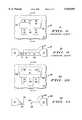
- FIG. 7is an enlarged top view of a semiconductor device 120 at an early stage in the manufacturing process.
- Semiconductor device 120is preferably formed in an SOI substrate 135, but it should be understood that the present invention may have application to devices formed in other semiconductor substrates such as a silicon substrate or a compound semiconductor substrate.
- Semiconductor device 120is formed in an active area 122 that is insulated by a field oxide region 121.
- active area 122is lightly doped, P--, and has a doping concentration less than about 1 ⁇ 10 16 atoms/cm 3 .
- At least a portion of active area 122is doped with a p-type dopant such a boron to enhance the electrical characteristics of semiconductor device 120.
- a photolithographic processis used to form an implant mask that exposes a portion of active area 122.
- the portion of active area 122 that is exposedis indicted in FIG. 7 with a dashed line 123. This pattern is defined by exposing a photosensitive material to light through a reticle.
- a conventional implant processis then used to doped at least a portion 124 of active area 122 so that it has a doping concentration of less than about 1 ⁇ 10 19 atoms/cm 3 and greater than about 1 ⁇ 10 16 atoms/cm 3 .
- This portion 124 of active area 122is indicated in FIG. 7 with the symbol "P-". It should also be understood that it is may be desirable to implant all of active area 122 with a threshold adjust implant, in which case, dashed line 123 would border or be outside active area 122.
- gate structure 129is partitioned with dashed lines into sub-regions 160-163 to explain the relative purpose of each section of gate structure 129 and how gate structure 129 effective divides active area 122,
- sub-regions 160 and 161are used to modulate a channel region 126 in active area 122 that is between a source region 127 and a drain region 128.
- Sub-regions 162 and 163are used to physically isolate a portion of active area 122 that will be a channel contact region 131 from source region 127 and drain region 128, respectively. If desired, it should also be understood that it is possible to perform the threshold adjust implant step shown in FIG. 7 after the formation of gate structure 129.
- semiconductor device 120continues with the doping of source region 127 and drain region 128 with an n-type dopant such as phosphorus.
- This doping processinvolves the formation of an implant mask to select the portions of active area 122 that are to be doped with the n-type dopant.
- Another reticleis used in combination with a photolithographic process to provide the implant mask.
- the portion of active area 122 to be implantedis indicated in FIG. 9 with a dashed line 150.
- the reticle used to define this pattern(dashed line 150) is different than the reticle used to define portion 124 of FIG. 7 (dashed line 123).
- the process of forming semiconductor device 120 in accordance with the present inventioncontinues as shown in FIG. 10.
- the portion of active area 122 that provides channel contact region 131is doped with a p-type dopant such as boron using an implant process.
- Another reticleis used in combination with a photolithographic process to define an implant mask as indicated in FIG. 10 with a dashed line 130.
- a conventional implant processis used to dope channel contact region 131 so that it preferably has a P+ doping concentration that is equal to or greater than about 1 ⁇ 10 19 atoms/cm 3 .
- Semiconductor device 120is operated by placing a voltage potential on gate structure 129, thereby allowing a current to flow from source region 127 to drain region 128.
- semiconductor device 120is formed in an SOI substrate.
- Channel contact region 131is used to place a voltage potential on or near channel region 126 to remove holes that collect in channel region 126 when semiconductor device 120 is in operation.
- FIG. 11is an enlarged cross-sectional view of semiconductor device 120 after completion of the steps shown in FIGS. 7-10.
- the cross-section shown in FIG. 11is taken along sectional lines 11--11 shown in FIG. 10.
- sub-regions 160 and 161overlie channel region 126, which has an essentially constant doping concentration in all portions of channel region 126 that are under gate structure 129.
- This profileresults from the fact that the entire channel region 126 is doped to a P- concentration level.
- the doping concentration across channel region 126is not exactly constant as slight variations due to non-uniform diffusion of dopant are expected by one skilled in the art.
- the structure of the present inventiondiffers from conventional FETs in that the lightly doped portion 32 (see FIG. 6) common to conventional FETs has been eliminated.
- semiconductor device 120transitions from a non-conductive to a conductive state in a more uniform manner and without the parasitic affects of a "kink" region.
- This improvementis illustrated in graph 110 of FIG. 12.
- Graph 110represents the output of a semiconductor device formed in accordance with the present invention.
- a y-axis 114is used to show the output current of the semiconductor device in amps (A) as the gate voltage, V g , is varied along an x-axis 115.
- Line 111represents the output of the semiconductor device, and as shown, is devoid of the "kink" region (see FIG. 1, bracket 13) that is common to conventional FETs formed in SOI substrates.
- transition region from a non-conductive state to a conductive state of the semiconductor deviceis also significantly narrower.
- the transition regionis indicated in graph 110 with a bracket 112. Consequently, a semiconductor device formed in accordance with the present invention is more linear and more tolerant to noise.
- the output current of the semiconductor deviceincreases monotonically during the transition from a non-conductive to a conductive state (bracket 112).
- the removal of the parasitic channel region that occurs in conventional devicesresults in a device that has less leakage current.
- the output currentis on the order of about 1 ⁇ 10 11 A. This is in contrast to a value of about 1 ⁇ 10 -7 A with comparable FET devices formed in SOI substrates using the conventional processing techniques (see FIG. 1).
- FIGS. 13-15illustrate enlarged top views of semiconductor devices 170, 180, and 190, respectively, that are formed in accordance with alternate embodiments of the present invention.
- semiconductor device 170 in FIG. 13is formed such that its gate structure 173 is arranged in an "I" configuration instead of the ⁇ T ⁇ configuration as shown in FIG. 10.
- This arrangementmay be desirable if semiconductor device 170 is formed without the use of a silicidation process to form electrical connection to a source region 174 and a drain region 175.
- a channel contact region 172is in direct contact with source region 174 and drain region 175. This results in the formation of a PN junction between channel contact region 172 and source region 174 and between channel contact region 172 and drain region 175.
- a semiconductor device 180as shown in FIG. 14 so that its gate structure 181 is in an ⁇ H ⁇ configuration. This may be desirable to enhance the removal of holes through channel contact regions 182 as a current flows from a source region 183 to a drain region 184.
- the present inventioncan also be used to form a semiconductor device 190 as shown in FIG. 15 such that channel contact regions 191 are on the same side of a gate structure 192 as a source region 193. Therefore, channel contact regions 191 would be on the opposite side of gate structure 192 as a drain region 194.
- the present inventionprovides a method of forming a semiconductor device that does not have a parasitic channel region and which does not suffer from the "kink” problem.
Landscapes
- Thin Film Transistor (AREA)
Abstract
Description
Claims (17)
Priority Applications (2)
| Application Number | Priority Date | Filing Date | Title |
|---|---|---|---|
| US08/834,964US5920093A (en) | 1997-04-07 | 1997-04-07 | SOI FET having gate sub-regions conforming to t-shape |
| JP10111455AJPH10284736A (en) | 1997-04-07 | 1998-04-07 | Semiconductor device and manufacturing method thereof |
Applications Claiming Priority (1)
| Application Number | Priority Date | Filing Date | Title |
|---|---|---|---|
| US08/834,964US5920093A (en) | 1997-04-07 | 1997-04-07 | SOI FET having gate sub-regions conforming to t-shape |
Publications (1)
| Publication Number | Publication Date |
|---|---|
| US5920093Atrue US5920093A (en) | 1999-07-06 |
Family
ID=25268231
Family Applications (1)
| Application Number | Title | Priority Date | Filing Date |
|---|---|---|---|
| US08/834,964Expired - LifetimeUS5920093A (en) | 1997-04-07 | 1997-04-07 | SOI FET having gate sub-regions conforming to t-shape |
Country Status (2)
| Country | Link |
|---|---|
| US (1) | US5920093A (en) |
| JP (1) | JPH10284736A (en) |
Cited By (30)
| Publication number | Priority date | Publication date | Assignee | Title |
|---|---|---|---|---|
| US6166786A (en)* | 1997-05-08 | 2000-12-26 | Hitachi, Ltd. | Semiconductor element with N channel and P region connected only to the channel and liquid crystal display device using the same |
| WO2001048828A1 (en)* | 1999-12-28 | 2001-07-05 | Honeywell Inc. | L- and u-gate devices for soi/sos applications |
| EP1143527A1 (en)* | 2000-04-04 | 2001-10-10 | Sharp Kabushiki Kaisha | Semiconductor device of soi structure |
| SG85660A1 (en)* | 1998-08-07 | 2002-01-15 | Ibm | Method and improved soi body contact structure for transistors |
| WO2002003468A3 (en)* | 2000-06-28 | 2002-04-11 | Advanced Micro Devices Inc | A novel capacitively coupled dtmos on soi |
| US6609214B1 (en) | 1999-08-23 | 2003-08-19 | International Business Machines Corporation | Method, system and program products for copying coupling facility structures |
| US6642579B2 (en)* | 2001-08-28 | 2003-11-04 | International Business Machines Corporation | Method of reducing the extrinsic body resistance in a silicon-on-insulator body contacted MOSFET |
| US20030222313A1 (en)* | 2002-05-30 | 2003-12-04 | Honeywell International Inc. | Self-aligned body tie for a partially depleted SOI device structure |
| US20040241969A1 (en)* | 2003-05-28 | 2004-12-02 | Advanced Micro Devices, Inc. | Body-tied SOI transistor and method for fabrication thereof |
| US20050072975A1 (en)* | 2003-10-02 | 2005-04-07 | Shiao-Shien Chen | Partially depleted soi mosfet device |
| EP1642339A1 (en)* | 2003-07-08 | 2006-04-05 | Seiko Epson Corporation | Semiconductor device |
| CN100416839C (en)* | 2003-10-13 | 2008-09-03 | 联华电子股份有限公司 | Partially depleted SOI MOS device |
| US20090283832A1 (en)* | 2008-05-16 | 2009-11-19 | Kabushiki Kaisha Toshiba | Semiconductor device |
| US7940706B2 (en) | 2001-10-01 | 2011-05-10 | International Business Machines Corporation | Controlling the state of duplexing of coupling facility structures |
| CN102117834A (en)* | 2011-01-19 | 2011-07-06 | 北京大学 | Multiple source MOS transistor with impurity segregation and production method thereof |
| US20110227637A1 (en)* | 2005-07-11 | 2011-09-22 | Stuber Michael A | Method and Apparatus Improving Gate Oxide Reliability by Controlling Accumulated Charge |
| US8742502B2 (en) | 2005-07-11 | 2014-06-03 | Peregrine Semiconductor Corporation | Method and apparatus for use in improving linearity of MOSFETs using an accumulated charge sink-harmonic wrinkle reduction |
| US9130564B2 (en) | 2005-07-11 | 2015-09-08 | Peregrine Semiconductor Corporation | Method and apparatus for use in improving linearity of MOSFETs using an accumulated charge sink |
| US9225378B2 (en) | 2001-10-10 | 2015-12-29 | Peregrine Semiconductor Corpopration | Switch circuit and method of switching radio frequency signals |
| US9419565B2 (en) | 2013-03-14 | 2016-08-16 | Peregrine Semiconductor Corporation | Hot carrier injection compensation |
| US9590674B2 (en) | 2012-12-14 | 2017-03-07 | Peregrine Semiconductor Corporation | Semiconductor devices with switchable ground-body connection |
| US9831857B2 (en) | 2015-03-11 | 2017-11-28 | Peregrine Semiconductor Corporation | Power splitter with programmable output phase shift |
| US10236872B1 (en) | 2018-03-28 | 2019-03-19 | Psemi Corporation | AC coupling modules for bias ladders |
| US10505530B2 (en) | 2018-03-28 | 2019-12-10 | Psemi Corporation | Positive logic switch with selectable DC blocking circuit |
| US10804892B2 (en) | 2005-07-11 | 2020-10-13 | Psemi Corporation | Circuit and method for controlling charge injection in radio frequency switches |
| WO2020237717A1 (en)* | 2019-05-31 | 2020-12-03 | 苏州大学 | Kink current calculation method and apparatus for soi device |
| US10886911B2 (en) | 2018-03-28 | 2021-01-05 | Psemi Corporation | Stacked FET switch bias ladders |
| US11011633B2 (en) | 2005-07-11 | 2021-05-18 | Psemi Corporation | Method and apparatus for use in improving linearity of MOSFETs using an accumulated charge sink-harmonic wrinkle reduction |
| USRE48965E1 (en) | 2005-07-11 | 2022-03-08 | Psemi Corporation | Method and apparatus improving gate oxide reliability by controlling accumulated charge |
| US11476849B2 (en) | 2020-01-06 | 2022-10-18 | Psemi Corporation | High power positive logic switch |
Citations (3)
| Publication number | Priority date | Publication date | Assignee | Title |
|---|---|---|---|---|
| US5001528A (en)* | 1989-01-31 | 1991-03-19 | The United States Of America As Represented By The Secretary Of The Air Force | Radiation hardened CMOS on SOI or SOS devices |
| US5604360A (en)* | 1992-12-04 | 1997-02-18 | Semiconductor Energy Laboratory Co., Ltd. | Semiconductor device including a plurality of thin film transistors at least some of which have a crystalline silicon film crystal-grown substantially in parallel to the surface of a substrate for the transistor |
| US5656844A (en)* | 1995-07-27 | 1997-08-12 | Motorola, Inc. | Semiconductor-on-insulator transistor having a doping profile for fully-depleted operation |
- 1997
- 1997-04-07USUS08/834,964patent/US5920093A/ennot_activeExpired - Lifetime
- 1998
- 1998-04-07JPJP10111455Apatent/JPH10284736A/enactivePending
Patent Citations (3)
| Publication number | Priority date | Publication date | Assignee | Title |
|---|---|---|---|---|
| US5001528A (en)* | 1989-01-31 | 1991-03-19 | The United States Of America As Represented By The Secretary Of The Air Force | Radiation hardened CMOS on SOI or SOS devices |
| US5604360A (en)* | 1992-12-04 | 1997-02-18 | Semiconductor Energy Laboratory Co., Ltd. | Semiconductor device including a plurality of thin film transistors at least some of which have a crystalline silicon film crystal-grown substantially in parallel to the surface of a substrate for the transistor |
| US5656844A (en)* | 1995-07-27 | 1997-08-12 | Motorola, Inc. | Semiconductor-on-insulator transistor having a doping profile for fully-depleted operation |
Cited By (62)
| Publication number | Priority date | Publication date | Assignee | Title |
|---|---|---|---|---|
| US6611300B1 (en) | 1997-05-08 | 2003-08-26 | Hitachi, Ltd. | Semiconductor element and liquid crystal display device using the same |
| US7002212B2 (en) | 1997-05-08 | 2006-02-21 | Hitachi, Ltd. | Static RAM having a TFT with n-type source and drain regions and a p-type region in contact with only the intrinsic channel of the same |
| US6166786A (en)* | 1997-05-08 | 2000-12-26 | Hitachi, Ltd. | Semiconductor element with N channel and P region connected only to the channel and liquid crystal display device using the same |
| US20040212752A1 (en)* | 1997-05-08 | 2004-10-28 | Tatsuya Ohkubo | Semiconductor element and liquid crystal display device using the same |
| SG85660A1 (en)* | 1998-08-07 | 2002-01-15 | Ibm | Method and improved soi body contact structure for transistors |
| US9565013B2 (en) | 1998-09-10 | 2017-02-07 | International Business Machines Corporation | Controlling the state of duplexing of coupling facility structures |
| US9253046B2 (en) | 1998-09-10 | 2016-02-02 | International Business Machines Corporation | Controlling the state of duplexing of coupling facility structures |
| US9860315B2 (en) | 1998-09-10 | 2018-01-02 | International Business Machines Corporation | Controlling the state of duplexing of coupling facility structures |
| US6609214B1 (en) | 1999-08-23 | 2003-08-19 | International Business Machines Corporation | Method, system and program products for copying coupling facility structures |
| EP1783836A3 (en)* | 1999-12-28 | 2008-02-27 | Honeywell, Inc. | L- and U-gate devices for SOI/SOS applications |
| US6307237B1 (en) | 1999-12-28 | 2001-10-23 | Honeywell International Inc. | L-and U-gate devices for SOI/SOS applications |
| WO2001048828A1 (en)* | 1999-12-28 | 2001-07-05 | Honeywell Inc. | L- and u-gate devices for soi/sos applications |
| US6693326B2 (en) | 2000-04-04 | 2004-02-17 | Sharp Kabushiki Kaisha | Semiconductor device of SOI structure |
| EP1143527A1 (en)* | 2000-04-04 | 2001-10-10 | Sharp Kabushiki Kaisha | Semiconductor device of soi structure |
| US6420767B1 (en) | 2000-06-28 | 2002-07-16 | Advanced Micro Devices, Inc. | Capacitively coupled DTMOS on SOI |
| WO2002003468A3 (en)* | 2000-06-28 | 2002-04-11 | Advanced Micro Devices Inc | A novel capacitively coupled dtmos on soi |
| US6642579B2 (en)* | 2001-08-28 | 2003-11-04 | International Business Machines Corporation | Method of reducing the extrinsic body resistance in a silicon-on-insulator body contacted MOSFET |
| US8341188B2 (en) | 2001-10-01 | 2012-12-25 | International Business Machines Corporation | Controlling the state of duplexing of coupling facility structures |
| US10491675B2 (en) | 2001-10-01 | 2019-11-26 | International Business Machines Corporation | Controlling the state of duplexing of coupling facility structures |
| US7940706B2 (en) | 2001-10-01 | 2011-05-10 | International Business Machines Corporation | Controlling the state of duplexing of coupling facility structures |
| US10812068B2 (en) | 2001-10-10 | 2020-10-20 | Psemi Corporation | Switch circuit and method of switching radio frequency signals |
| US9225378B2 (en) | 2001-10-10 | 2015-12-29 | Peregrine Semiconductor Corpopration | Switch circuit and method of switching radio frequency signals |
| US10797694B2 (en) | 2001-10-10 | 2020-10-06 | Psemi Corporation | Switch circuit and method of switching radio frequency signals |
| US7192816B2 (en) | 2002-05-30 | 2007-03-20 | Honeywell International Inc. | Self-aligned body tie for a partially depleted SOI device structure |
| US6960810B2 (en) | 2002-05-30 | 2005-11-01 | Honeywell International Inc. | Self-aligned body tie for a partially depleted SOI device structure |
| US20050173764A1 (en)* | 2002-05-30 | 2005-08-11 | Honeywell International Inc. | Self-aligned body tie for a partially depletion SOI device structure |
| US20030222313A1 (en)* | 2002-05-30 | 2003-12-04 | Honeywell International Inc. | Self-aligned body tie for a partially depleted SOI device structure |
| US7138318B2 (en)* | 2003-05-28 | 2006-11-21 | Advanced Micro Devices, Inc. | Method of fabricating body-tied SOI transistor having halo implant region underlying hammerhead portion of gate |
| WO2005015644A1 (en)* | 2003-05-28 | 2005-02-17 | Advanced Micro Devices, Inc. | Body-tied soi transistor and method for fabrication thereof |
| US20040241969A1 (en)* | 2003-05-28 | 2004-12-02 | Advanced Micro Devices, Inc. | Body-tied SOI transistor and method for fabrication thereof |
| EP1642339A1 (en)* | 2003-07-08 | 2006-04-05 | Seiko Epson Corporation | Semiconductor device |
| US20050072975A1 (en)* | 2003-10-02 | 2005-04-07 | Shiao-Shien Chen | Partially depleted soi mosfet device |
| CN100416839C (en)* | 2003-10-13 | 2008-09-03 | 联华电子股份有限公司 | Partially depleted SOI MOS device |
| US8742502B2 (en) | 2005-07-11 | 2014-06-03 | Peregrine Semiconductor Corporation | Method and apparatus for use in improving linearity of MOSFETs using an accumulated charge sink-harmonic wrinkle reduction |
| USRE48944E1 (en) | 2005-07-11 | 2022-02-22 | Psemi Corporation | Method and apparatus for use in improving linearity of MOSFETS using an accumulated charge sink |
| US9087899B2 (en) | 2005-07-11 | 2015-07-21 | Peregrine Semiconductor Corporation | Method and apparatus for use in improving linearity of MOSFETs using an accumulated charge sink-harmonic wrinkle reduction |
| US8954902B2 (en) | 2005-07-11 | 2015-02-10 | Peregrine Semiconductor Corporation | Method and apparatus improving gate oxide reliability by controlling accumulated charge |
| US12074217B2 (en) | 2005-07-11 | 2024-08-27 | Psemi Corporation | Method and apparatus for use in improving linearity of MOSFETs using an accumulated charge sink-harmonic wrinkle reduction |
| USRE48965E1 (en) | 2005-07-11 | 2022-03-08 | Psemi Corporation | Method and apparatus improving gate oxide reliability by controlling accumulated charge |
| US9130564B2 (en) | 2005-07-11 | 2015-09-08 | Peregrine Semiconductor Corporation | Method and apparatus for use in improving linearity of MOSFETs using an accumulated charge sink |
| US9608619B2 (en) | 2005-07-11 | 2017-03-28 | Peregrine Semiconductor Corporation | Method and apparatus improving gate oxide reliability by controlling accumulated charge |
| US11011633B2 (en) | 2005-07-11 | 2021-05-18 | Psemi Corporation | Method and apparatus for use in improving linearity of MOSFETs using an accumulated charge sink-harmonic wrinkle reduction |
| US10804892B2 (en) | 2005-07-11 | 2020-10-13 | Psemi Corporation | Circuit and method for controlling charge injection in radio frequency switches |
| US10797691B1 (en) | 2005-07-11 | 2020-10-06 | Psemi Corporation | Method and apparatus for use in improving linearity of MOSFETs using an accumulated charge sink |
| US20110227637A1 (en)* | 2005-07-11 | 2011-09-22 | Stuber Michael A | Method and Apparatus Improving Gate Oxide Reliability by Controlling Accumulated Charge |
| US8072030B2 (en)* | 2008-05-16 | 2011-12-06 | Kabushiki Kaisha Toshiba | Semiconductor device |
| US20090283832A1 (en)* | 2008-05-16 | 2009-11-19 | Kabushiki Kaisha Toshiba | Semiconductor device |
| CN102117834A (en)* | 2011-01-19 | 2011-07-06 | 北京大学 | Multiple source MOS transistor with impurity segregation and production method thereof |
| CN102117834B (en)* | 2011-01-19 | 2012-12-19 | 北京大学 | Multiple source MOS transistor with impurity segregation and production method thereof |
| US9590674B2 (en) | 2012-12-14 | 2017-03-07 | Peregrine Semiconductor Corporation | Semiconductor devices with switchable ground-body connection |
| US9419565B2 (en) | 2013-03-14 | 2016-08-16 | Peregrine Semiconductor Corporation | Hot carrier injection compensation |
| US9831857B2 (en) | 2015-03-11 | 2017-11-28 | Peregrine Semiconductor Corporation | Power splitter with programmable output phase shift |
| US10886911B2 (en) | 2018-03-28 | 2021-01-05 | Psemi Corporation | Stacked FET switch bias ladders |
| US10505530B2 (en) | 2018-03-28 | 2019-12-10 | Psemi Corporation | Positive logic switch with selectable DC blocking circuit |
| US11018662B2 (en) | 2018-03-28 | 2021-05-25 | Psemi Corporation | AC coupling modules for bias ladders |
| US10862473B2 (en) | 2018-03-28 | 2020-12-08 | Psemi Corporation | Positive logic switch with selectable DC blocking circuit |
| US11418183B2 (en) | 2018-03-28 | 2022-08-16 | Psemi Corporation | AC coupling modules for bias ladders |
| US11870431B2 (en) | 2018-03-28 | 2024-01-09 | Psemi Corporation | AC coupling modules for bias ladders |
| US10236872B1 (en) | 2018-03-28 | 2019-03-19 | Psemi Corporation | AC coupling modules for bias ladders |
| WO2020237717A1 (en)* | 2019-05-31 | 2020-12-03 | 苏州大学 | Kink current calculation method and apparatus for soi device |
| US11476849B2 (en) | 2020-01-06 | 2022-10-18 | Psemi Corporation | High power positive logic switch |
| US12081211B2 (en) | 2020-01-06 | 2024-09-03 | Psemi Corporation | High power positive logic switch |
Also Published As
| Publication number | Publication date |
|---|---|
| JPH10284736A (en) | 1998-10-23 |
Similar Documents
| Publication | Publication Date | Title |
|---|---|---|
| US5920093A (en) | SOI FET having gate sub-regions conforming to t-shape | |
| US6958519B2 (en) | Methods of forming field effect transistors and field effect transistor circuitry | |
| US6031268A (en) | Complementary semiconductor device and method for producing the same | |
| JP3455452B2 (en) | Semiconductor device and manufacturing method thereof | |
| EP0248292B1 (en) | Semiconductor device having a high breakdown voltage | |
| KR960012539A (en) | Semiconductor device and manufacturing method | |
| KR100611111B1 (en) | High frequency MOS transistor, method for forming same and method for manufacturing semiconductor device | |
| KR100391959B1 (en) | Semiconductor apparatus and method of manufacture | |
| KR970060534A (en) | Power semiconductor device and manufacturing method thereof | |
| US6054357A (en) | Semiconductor device and method for fabricating the same | |
| US5827763A (en) | Method of forming a multiple transistor channel doping using a dual resist fabrication sequence | |
| US5879995A (en) | High-voltage transistor and manufacturing method therefor | |
| US5623154A (en) | Semiconductor device having triple diffusion | |
| US4282539A (en) | Field effect transistor with decreased substrate control of the channel width | |
| US6150200A (en) | Semiconductor device and method of making | |
| KR100301071B1 (en) | DMOS transistor and method for manufacturing thereof | |
| JP3058604B2 (en) | Semiconductor device having double junction structure and method of manufacturing the same | |
| KR19980702335A (en) | A method of manufacturing a resurf semiconductor device and a semiconductor device manufactured by such a method | |
| KR100375600B1 (en) | Transistor and method for manufacturing the same | |
| US7335549B2 (en) | Semiconductor device and method for fabricating the same | |
| US6096606A (en) | Method of making a semiconductor device | |
| KR100230358B1 (en) | Silicon-on-Insulator Device and Manufacturing Method Thereof | |
| KR100304718B1 (en) | A power semiconductor device and method for manufacturing thereof | |
| KR0167606B1 (en) | Process of fabricating mos-transistor | |
| KR0147649B1 (en) | Method of fabricating a non-volatile memory device |
Legal Events
| Date | Code | Title | Description |
|---|---|---|---|
| AS | Assignment | Owner name:MOTOROLA, INC., ILLINOIS Free format text:ASSIGNMENT OF ASSIGNORS INTEREST;ASSIGNORS:HUANG, WEN LING MARGARET;TSENG, YING-CHE;REEL/FRAME:008496/0961 Effective date:19970326 | |
| STCF | Information on status: patent grant | Free format text:PATENTED CASE | |
| FPAY | Fee payment | Year of fee payment:4 | |
| AS | Assignment | Owner name:FREESCALE SEMICONDUCTOR, INC., TEXAS Free format text:ASSIGNMENT OF ASSIGNORS INTEREST;ASSIGNOR:MOTOROLA, INC.;REEL/FRAME:015698/0657 Effective date:20040404 Owner name:FREESCALE SEMICONDUCTOR, INC.,TEXAS Free format text:ASSIGNMENT OF ASSIGNORS INTEREST;ASSIGNOR:MOTOROLA, INC.;REEL/FRAME:015698/0657 Effective date:20040404 | |
| FPAY | Fee payment | Year of fee payment:8 | |
| AS | Assignment | Owner name:CITIBANK, N.A. AS COLLATERAL AGENT, NEW YORK Free format text:SECURITY AGREEMENT;ASSIGNORS:FREESCALE SEMICONDUCTOR, INC.;FREESCALE ACQUISITION CORPORATION;FREESCALE ACQUISITION HOLDINGS CORP.;AND OTHERS;REEL/FRAME:018855/0129 Effective date:20061201 Owner name:CITIBANK, N.A. AS COLLATERAL AGENT,NEW YORK Free format text:SECURITY AGREEMENT;ASSIGNORS:FREESCALE SEMICONDUCTOR, INC.;FREESCALE ACQUISITION CORPORATION;FREESCALE ACQUISITION HOLDINGS CORP.;AND OTHERS;REEL/FRAME:018855/0129 Effective date:20061201 | |
| AS | Assignment | Owner name:CITIBANK, N.A., AS COLLATERAL AGENT,NEW YORK Free format text:SECURITY AGREEMENT;ASSIGNOR:FREESCALE SEMICONDUCTOR, INC.;REEL/FRAME:024397/0001 Effective date:20100413 Owner name:CITIBANK, N.A., AS COLLATERAL AGENT, NEW YORK Free format text:SECURITY AGREEMENT;ASSIGNOR:FREESCALE SEMICONDUCTOR, INC.;REEL/FRAME:024397/0001 Effective date:20100413 | |
| FPAY | Fee payment | Year of fee payment:12 | |
| AS | Assignment | Owner name:CITIBANK, N.A., AS NOTES COLLATERAL AGENT, NEW YORK Free format text:SECURITY AGREEMENT;ASSIGNOR:FREESCALE SEMICONDUCTOR, INC.;REEL/FRAME:030633/0424 Effective date:20130521 Owner name:CITIBANK, N.A., AS NOTES COLLATERAL AGENT, NEW YOR Free format text:SECURITY AGREEMENT;ASSIGNOR:FREESCALE SEMICONDUCTOR, INC.;REEL/FRAME:030633/0424 Effective date:20130521 | |
| AS | Assignment | Owner name:CITIBANK, N.A., AS NOTES COLLATERAL AGENT, NEW YORK Free format text:SECURITY AGREEMENT;ASSIGNOR:FREESCALE SEMICONDUCTOR, INC.;REEL/FRAME:031591/0266 Effective date:20131101 Owner name:CITIBANK, N.A., AS NOTES COLLATERAL AGENT, NEW YOR Free format text:SECURITY AGREEMENT;ASSIGNOR:FREESCALE SEMICONDUCTOR, INC.;REEL/FRAME:031591/0266 Effective date:20131101 | |
| AS | Assignment | Owner name:FREESCALE SEMICONDUCTOR, INC., TEXAS Free format text:PATENT RELEASE;ASSIGNOR:CITIBANK, N.A., AS COLLATERAL AGENT;REEL/FRAME:037354/0225 Effective date:20151207 Owner name:FREESCALE SEMICONDUCTOR, INC., TEXAS Free format text:PATENT RELEASE;ASSIGNOR:CITIBANK, N.A., AS COLLATERAL AGENT;REEL/FRAME:037356/0553 Effective date:20151207 Owner name:FREESCALE SEMICONDUCTOR, INC., TEXAS Free format text:PATENT RELEASE;ASSIGNOR:CITIBANK, N.A., AS COLLATERAL AGENT;REEL/FRAME:037356/0143 Effective date:20151207 | |
| AS | Assignment | Owner name:MORGAN STANLEY SENIOR FUNDING, INC., MARYLAND Free format text:ASSIGNMENT AND ASSUMPTION OF SECURITY INTEREST IN PATENTS;ASSIGNOR:CITIBANK, N.A.;REEL/FRAME:037486/0517 Effective date:20151207 | |
| AS | Assignment | Owner name:MORGAN STANLEY SENIOR FUNDING, INC., MARYLAND Free format text:ASSIGNMENT AND ASSUMPTION OF SECURITY INTEREST IN PATENTS;ASSIGNOR:CITIBANK, N.A.;REEL/FRAME:037518/0292 Effective date:20151207 | |
| AS | Assignment | Owner name:MORGAN STANLEY SENIOR FUNDING, INC., MARYLAND Free format text:SUPPLEMENT TO THE SECURITY AGREEMENT;ASSIGNOR:FREESCALE SEMICONDUCTOR, INC.;REEL/FRAME:039138/0001 Effective date:20160525 | |
| AS | Assignment | Owner name:NXP, B.V., F/K/A FREESCALE SEMICONDUCTOR, INC., NETHERLANDS Free format text:RELEASE BY SECURED PARTY;ASSIGNOR:MORGAN STANLEY SENIOR FUNDING, INC.;REEL/FRAME:040925/0001 Effective date:20160912 Owner name:NXP, B.V., F/K/A FREESCALE SEMICONDUCTOR, INC., NE Free format text:RELEASE BY SECURED PARTY;ASSIGNOR:MORGAN STANLEY SENIOR FUNDING, INC.;REEL/FRAME:040925/0001 Effective date:20160912 | |
| AS | Assignment | Owner name:NXP B.V., NETHERLANDS Free format text:RELEASE BY SECURED PARTY;ASSIGNOR:MORGAN STANLEY SENIOR FUNDING, INC.;REEL/FRAME:040928/0001 Effective date:20160622 | |
| AS | Assignment | Owner name:NXP USA, INC., TEXAS Free format text:CHANGE OF NAME;ASSIGNOR:FREESCALE SEMICONDUCTOR, INC.;REEL/FRAME:040652/0241 Effective date:20161107 Owner name:NXP USA, INC., TEXAS Free format text:MERGER;ASSIGNOR:FREESCALE SEMICONDUCTOR, INC.;REEL/FRAME:040652/0241 Effective date:20161107 | |
| AS | Assignment | Owner name:NXP USA, INC., TEXAS Free format text:CORRECTIVE ASSIGNMENT TO CORRECT THE NATURE OF CONVEYANCE PREVIOUSLY RECORDED AT REEL: 040652 FRAME: 0241. ASSIGNOR(S) HEREBY CONFIRMS THE MERGER AND CHANGE OF NAME;ASSIGNOR:FREESCALE SEMICONDUCTOR, INC.;REEL/FRAME:041260/0850 Effective date:20161107 | |
| AS | Assignment | Owner name:MORGAN STANLEY SENIOR FUNDING, INC., MARYLAND Free format text:CORRECTIVE ASSIGNMENT TO CORRECT THE REMOVE PATENTS 8108266 AND 8062324 AND REPLACE THEM WITH 6108266 AND 8060324 PREVIOUSLY RECORDED ON REEL 037518 FRAME 0292. ASSIGNOR(S) HEREBY CONFIRMS THE ASSIGNMENT AND ASSUMPTION OF SECURITY INTEREST IN PATENTS;ASSIGNOR:CITIBANK, N.A.;REEL/FRAME:041703/0536 Effective date:20151207 | |
| AS | Assignment | Owner name:SHENZHEN XINGUODU TECHNOLOGY CO., LTD., CHINA Free format text:CORRECTIVE ASSIGNMENT TO CORRECT THE TO CORRECT THE APPLICATION NO. FROM 13,883,290 TO 13,833,290 PREVIOUSLY RECORDED ON REEL 041703 FRAME 0536. ASSIGNOR(S) HEREBY CONFIRMS THE THE ASSIGNMENT AND ASSUMPTION OF SECURITYINTEREST IN PATENTS.;ASSIGNOR:MORGAN STANLEY SENIOR FUNDING, INC.;REEL/FRAME:048734/0001 Effective date:20190217 | |
| AS | Assignment | Owner name:NXP B.V., NETHERLANDS Free format text:RELEASE BY SECURED PARTY;ASSIGNOR:MORGAN STANLEY SENIOR FUNDING, INC.;REEL/FRAME:050744/0097 Effective date:20190903 | |
| AS | Assignment | Owner name:MORGAN STANLEY SENIOR FUNDING, INC., MARYLAND Free format text:CORRECTIVE ASSIGNMENT TO CORRECT THE REMOVE APPLICATION11759915 AND REPLACE IT WITH APPLICATION 11759935 PREVIOUSLY RECORDED ON REEL 037486 FRAME 0517. ASSIGNOR(S) HEREBY CONFIRMS THE ASSIGNMENT AND ASSUMPTION OF SECURITYINTEREST IN PATENTS;ASSIGNOR:CITIBANK, N.A.;REEL/FRAME:053547/0421 Effective date:20151207 | |
| AS | Assignment | Owner name:NXP B.V., NETHERLANDS Free format text:CORRECTIVE ASSIGNMENT TO CORRECT THE REMOVEAPPLICATION 11759915 AND REPLACE IT WITH APPLICATION11759935 PREVIOUSLY RECORDED ON REEL 040928 FRAME 0001. ASSIGNOR(S) HEREBY CONFIRMS THE RELEASE OF SECURITYINTEREST;ASSIGNOR:MORGAN STANLEY SENIOR FUNDING, INC.;REEL/FRAME:052915/0001 Effective date:20160622 | |
| AS | Assignment | Owner name:NXP, B.V. F/K/A FREESCALE SEMICONDUCTOR, INC., NETHERLANDS Free format text:CORRECTIVE ASSIGNMENT TO CORRECT THE REMOVEAPPLICATION 11759915 AND REPLACE IT WITH APPLICATION11759935 PREVIOUSLY RECORDED ON REEL 040925 FRAME 0001. ASSIGNOR(S) HEREBY CONFIRMS THE RELEASE OF SECURITYINTEREST;ASSIGNOR:MORGAN STANLEY SENIOR FUNDING, INC.;REEL/FRAME:052917/0001 Effective date:20160912 |