US5920080A - Emissive display using organic light emitting diodes - Google Patents
Emissive display using organic light emitting diodesDownload PDFInfo
- Publication number
- US5920080A US5920080AUS09/074,424US7442498AUS5920080AUS 5920080 AUS5920080 AUS 5920080AUS 7442498 AUS7442498 AUS 7442498AUS 5920080 AUS5920080 AUS 5920080A
- Authority
- US
- United States
- Prior art keywords
- layer
- conductor
- light emitting
- overlying
- layers
- Prior art date
- Legal status (The legal status is an assumption and is not a legal conclusion. Google has not performed a legal analysis and makes no representation as to the accuracy of the status listed.)
- Expired - Lifetime
Links
- 239000004020conductorSubstances0.000claimsabstractdescription80
- 239000000758substrateSubstances0.000claimsabstractdescription48
- 239000011368organic materialSubstances0.000claimsabstractdescription35
- 239000000463materialSubstances0.000claimsdescription35
- 230000004888barrier functionEffects0.000claimsdescription32
- 239000003989dielectric materialSubstances0.000claimsdescription32
- 238000007789sealingMethods0.000claimsdescription25
- XUIMIQQOPSSXEZ-UHFFFAOYSA-NSiliconChemical compound[Si]XUIMIQQOPSSXEZ-UHFFFAOYSA-N0.000claimsdescription12
- 239000010703siliconSubstances0.000claimsdescription12
- 229910052710siliconInorganic materials0.000claimsdescription12
- 230000007704transitionEffects0.000claimsdescription12
- XLYOFNOQVPJJNP-UHFFFAOYSA-NwaterSubstancesOXLYOFNOQVPJJNP-UHFFFAOYSA-N0.000claimsdescription5
- 239000000853adhesiveSubstances0.000claimsdescription4
- 230000001070adhesive effectEffects0.000claimsdescription4
- 239000003575carbonaceous materialSubstances0.000claimsdescription3
- OKTJSMMVPCPJKN-UHFFFAOYSA-NCarbonChemical compound[C]OKTJSMMVPCPJKN-UHFFFAOYSA-N0.000claimsdescription2
- 229910052799carbonInorganic materials0.000claimsdescription2
- 239000010410layerSubstances0.000abstractdescription159
- 230000001965increasing effectEffects0.000abstractdescription5
- 239000012044organic layerSubstances0.000abstractdescription5
- 230000002708enhancing effectEffects0.000abstractdescription2
- 239000011159matrix materialSubstances0.000description30
- VYPSYNLAJGMNEJ-UHFFFAOYSA-NSilicium dioxideChemical compoundO=[Si]=OVYPSYNLAJGMNEJ-UHFFFAOYSA-N0.000description18
- 238000000034methodMethods0.000description18
- 238000000151depositionMethods0.000description10
- 229910052782aluminiumInorganic materials0.000description8
- QVGXLLKOCUKJST-UHFFFAOYSA-Natomic oxygenChemical compound[O]QVGXLLKOCUKJST-UHFFFAOYSA-N0.000description8
- 238000001704evaporationMethods0.000description8
- 239000010408filmSubstances0.000description8
- 239000001301oxygenSubstances0.000description8
- 229910052760oxygenInorganic materials0.000description8
- 239000000377silicon dioxideSubstances0.000description8
- 230000008020evaporationEffects0.000description7
- 229910052751metalInorganic materials0.000description7
- 239000002184metalSubstances0.000description7
- 239000000203mixtureSubstances0.000description7
- 230000008569processEffects0.000description7
- XLOMVQKBTHCTTD-UHFFFAOYSA-NZinc monoxideChemical compound[Zn]=OXLOMVQKBTHCTTD-UHFFFAOYSA-N0.000description6
- XAGFODPZIPBFFR-UHFFFAOYSA-NaluminiumChemical compound[Al]XAGFODPZIPBFFR-UHFFFAOYSA-N0.000description6
- 238000002347injectionMethods0.000description6
- 239000007924injectionSubstances0.000description6
- 238000000623plasma-assisted chemical vapour depositionMethods0.000description6
- 230000005465channelingEffects0.000description5
- 238000006243chemical reactionMethods0.000description5
- 229910052749magnesiumInorganic materials0.000description5
- 239000011777magnesiumSubstances0.000description5
- XKRFYHLGVUSROY-UHFFFAOYSA-NArgonChemical compound[Ar]XKRFYHLGVUSROY-UHFFFAOYSA-N0.000description4
- 239000011651chromiumSubstances0.000description4
- 229910052681coesiteInorganic materials0.000description4
- 239000006059cover glassSubstances0.000description4
- 229910052906cristobaliteInorganic materials0.000description4
- 229910052744lithiumInorganic materials0.000description4
- 238000004519manufacturing processMethods0.000description4
- VNWKTOKETHGBQD-UHFFFAOYSA-NmethaneChemical compoundCVNWKTOKETHGBQD-UHFFFAOYSA-N0.000description4
- 235000012239silicon dioxideNutrition0.000description4
- 238000004544sputter depositionMethods0.000description4
- 229910052682stishoviteInorganic materials0.000description4
- 239000010936titaniumSubstances0.000description4
- 229910052719titaniumInorganic materials0.000description4
- 229910052905tridymiteInorganic materials0.000description4
- VYZAMTAEIAYCRO-UHFFFAOYSA-NChromiumChemical compound[Cr]VYZAMTAEIAYCRO-UHFFFAOYSA-N0.000description3
- 230000004913activationEffects0.000description3
- 229910052788bariumInorganic materials0.000description3
- 230000008901benefitEffects0.000description3
- UFVXQDWNSAGPHN-UHFFFAOYSA-Kbis[(2-methylquinolin-8-yl)oxy]-(4-phenylphenoxy)alumaneChemical compound[Al+3].C1=CC=C([O-])C2=NC(C)=CC=C21.C1=CC=C([O-])C2=NC(C)=CC=C21.C1=CC([O-])=CC=C1C1=CC=CC=C1UFVXQDWNSAGPHN-UHFFFAOYSA-K0.000description3
- 229910052792caesiumInorganic materials0.000description3
- 229910052791calciumInorganic materials0.000description3
- 239000011575calciumSubstances0.000description3
- 239000003086colorantSubstances0.000description3
- 230000008021depositionEffects0.000description3
- 238000013461designMethods0.000description3
- 238000005286illuminationMethods0.000description3
- 238000010849ion bombardmentMethods0.000description3
- 238000002156mixingMethods0.000description3
- 238000012986modificationMethods0.000description3
- 230000004048modificationEffects0.000description3
- 230000003647oxidationEffects0.000description3
- 238000007254oxidation reactionMethods0.000description3
- KDLHZDBZIXYQEI-UHFFFAOYSA-NpalladiumSubstances[Pd]KDLHZDBZIXYQEI-UHFFFAOYSA-N0.000description3
- 230000036961partial effectEffects0.000description3
- 125000002080perylenyl groupChemical groupC1(=CC=C2C=CC=C3C4=CC=CC5=CC=CC(C1=C23)=C45)*0.000description3
- CSHWQDPOILHKBI-UHFFFAOYSA-NperyreneNatural productsC1=CC(C2=CC=CC=3C2=C2C=CC=3)=C3C2=CC=CC3=C1CSHWQDPOILHKBI-UHFFFAOYSA-N0.000description3
- 230000004044responseEffects0.000description3
- HBMJWWWQQXIZIP-UHFFFAOYSA-Nsilicon carbideChemical compound[Si+]#[C-]HBMJWWWQQXIZIP-UHFFFAOYSA-N0.000description3
- 239000007787solidSubstances0.000description3
- 239000010409thin filmSubstances0.000description3
- 239000011787zinc oxideSubstances0.000description3
- 229910000838Al alloyInorganic materials0.000description2
- IJGRMHOSHXDMSA-UHFFFAOYSA-NAtomic nitrogenChemical compoundN#NIJGRMHOSHXDMSA-UHFFFAOYSA-N0.000description2
- OYPRJOBELJOOCE-UHFFFAOYSA-NCalciumChemical compound[Ca]OYPRJOBELJOOCE-UHFFFAOYSA-N0.000description2
- 239000004593EpoxySubstances0.000description2
- WHXSMMKQMYFTQS-UHFFFAOYSA-NLithiumChemical compound[Li]WHXSMMKQMYFTQS-UHFFFAOYSA-N0.000description2
- FYYHWMGAXLPEAU-UHFFFAOYSA-NMagnesiumChemical compound[Mg]FYYHWMGAXLPEAU-UHFFFAOYSA-N0.000description2
- RTAQQCXQSZGOHL-UHFFFAOYSA-NTitaniumChemical compound[Ti]RTAQQCXQSZGOHL-UHFFFAOYSA-N0.000description2
- MCMNRKCIXSYSNV-UHFFFAOYSA-NZirconium dioxideChemical compoundO=[Zr]=OMCMNRKCIXSYSNV-UHFFFAOYSA-N0.000description2
- 229910003481amorphous carbonInorganic materials0.000description2
- 229910052786argonInorganic materials0.000description2
- 229910052804chromiumInorganic materials0.000description2
- 238000000576coating methodMethods0.000description2
- XCJYREBRNVKWGJ-UHFFFAOYSA-Ncopper(II) phthalocyanineChemical compound[Cu+2].C12=CC=CC=C2C(N=C2[N-]C(C3=CC=CC=C32)=N2)=NC1=NC([C]1C=CC=CC1=1)=NC=1N=C1[C]3C=CC=CC3=C2[N-]1XCJYREBRNVKWGJ-UHFFFAOYSA-N0.000description2
- 230000000593degrading effectEffects0.000description2
- 239000002019doping agentSubstances0.000description2
- 238000005516engineering processMethods0.000description2
- 239000012535impuritySubstances0.000description2
- 238000009616inductively coupled plasmaMethods0.000description2
- 239000012212insulatorSubstances0.000description2
- 150000002500ionsChemical class0.000description2
- 229910044991metal oxideInorganic materials0.000description2
- 150000004706metal oxidesChemical class0.000description2
- 239000003921oilSubstances0.000description2
- 229910052763palladiumInorganic materials0.000description2
- 238000005498polishingMethods0.000description2
- 229920000642polymerPolymers0.000description2
- 230000001681protective effectEffects0.000description2
- 230000009467reductionEffects0.000description2
- 239000011347resinSubstances0.000description2
- 229920005989resinPolymers0.000description2
- 239000004065semiconductorSubstances0.000description2
- 238000000926separation methodMethods0.000description2
- 229910010271silicon carbideInorganic materials0.000description2
- LIVNPJMFVYWSIS-UHFFFAOYSA-Nsilicon monoxideChemical compound[Si-]#[O+]LIVNPJMFVYWSIS-UHFFFAOYSA-N0.000description2
- 229910052814silicon oxideInorganic materials0.000description2
- 239000002904solventSubstances0.000description2
- 239000000126substanceSubstances0.000description2
- 230000002459sustained effectEffects0.000description2
- NIXOWILDQLNWCW-UHFFFAOYSA-MAcrylateChemical compound[O-]C(=O)C=CNIXOWILDQLNWCW-UHFFFAOYSA-M0.000description1
- 229910001148Al-Li alloyInorganic materials0.000description1
- 229910052692DysprosiumInorganic materials0.000description1
- 229910019015Mg-AgInorganic materials0.000description1
- 229910001182Mo alloyInorganic materials0.000description1
- 229910000611Zinc aluminiumInorganic materials0.000description1
- 238000002679ablationMethods0.000description1
- 239000011149active materialSubstances0.000description1
- 230000002411adverseEffects0.000description1
- 239000003513alkaliSubstances0.000description1
- 229910045601alloyInorganic materials0.000description1
- 239000000956alloySubstances0.000description1
- DSAJWYNOEDNPEQ-UHFFFAOYSA-Nbarium atomChemical compound[Ba]DSAJWYNOEDNPEQ-UHFFFAOYSA-N0.000description1
- JRPBQTZRNDNNOP-UHFFFAOYSA-Nbarium titanateChemical compound[Ba+2].[Ba+2].[O-][Ti]([O-])([O-])[O-]JRPBQTZRNDNNOP-UHFFFAOYSA-N0.000description1
- 229910002113barium titanateInorganic materials0.000description1
- 230000009286beneficial effectEffects0.000description1
- 230000005540biological transmissionEffects0.000description1
- 230000015572biosynthetic processEffects0.000description1
- TVFDJXOCXUVLDH-UHFFFAOYSA-Ncaesium atomChemical compound[Cs]TVFDJXOCXUVLDH-UHFFFAOYSA-N0.000description1
- 239000003990capacitorSubstances0.000description1
- 230000015556catabolic processEffects0.000description1
- 239000010406cathode materialSubstances0.000description1
- 239000000919ceramicSubstances0.000description1
- 229910000423chromium oxideInorganic materials0.000description1
- 239000011248coating agentSubstances0.000description1
- 150000001875compoundsChemical class0.000description1
- 238000010276constructionMethods0.000description1
- 239000000356contaminantSubstances0.000description1
- 229910052802copperInorganic materials0.000description1
- 238000000280densificationMethods0.000description1
- 239000002274desiccantSubstances0.000description1
- 238000011161developmentMethods0.000description1
- 238000002059diagnostic imagingMethods0.000description1
- KBQHZAAAGSGFKK-UHFFFAOYSA-Ndysprosium atomChemical compound[Dy]KBQHZAAAGSGFKK-UHFFFAOYSA-N0.000description1
- 238000005401electroluminescenceMethods0.000description1
- 239000011888foilSubstances0.000description1
- 239000007789gasSubstances0.000description1
- 239000011521glassSubstances0.000description1
- 229910052737goldInorganic materials0.000description1
- 229910002804graphiteInorganic materials0.000description1
- 239000010439graphiteSubstances0.000description1
- 238000010438heat treatmentMethods0.000description1
- 230000005525hole transportEffects0.000description1
- 239000001257hydrogenSubstances0.000description1
- 229910052739hydrogenInorganic materials0.000description1
- 125000004435hydrogen atomChemical class[H]*0.000description1
- 239000011261inert gasSubstances0.000description1
- 238000007737ion beam depositionMethods0.000description1
- 238000000608laser ablationMethods0.000description1
- 230000000670limiting effectEffects0.000description1
- 230000007774longtermEffects0.000description1
- 230000014759maintenance of locationEffects0.000description1
- 239000013212metal-organic materialSubstances0.000description1
- 150000002739metalsChemical class0.000description1
- 239000011533mixed conductorSubstances0.000description1
- 230000004297night visionEffects0.000description1
- 229910052757nitrogenInorganic materials0.000description1
- RVTZCBVAJQQJTK-UHFFFAOYSA-Noxygen(2-);zirconium(4+)Chemical compound[O-2].[O-2].[Zr+4]RVTZCBVAJQQJTK-UHFFFAOYSA-N0.000description1
- 238000004806packaging method and processMethods0.000description1
- 230000035515penetrationEffects0.000description1
- 229910052697platinumInorganic materials0.000description1
- 229920006254polymer filmPolymers0.000description1
- 238000007639printingMethods0.000description1
- 238000012545processingMethods0.000description1
- 230000002829reductive effectEffects0.000description1
- 229910052706scandiumInorganic materials0.000description1
- 229910052709silverInorganic materials0.000description1
- 239000005361soda-lime glassSubstances0.000description1
- 239000000243solutionSubstances0.000description1
- 238000001228spectrumMethods0.000description1
- 238000012546transferMethods0.000description1
- 239000012780transparent materialSubstances0.000description1
- WFKWXMTUELFFGS-UHFFFAOYSA-NtungstenChemical compound[W]WFKWXMTUELFFGS-UHFFFAOYSA-N0.000description1
- 229910052721tungstenInorganic materials0.000description1
- 239000010937tungstenSubstances0.000description1
- 229910001928zirconium oxideInorganic materials0.000description1
Images


Classifications
- H—ELECTRICITY
- H05—ELECTRIC TECHNIQUES NOT OTHERWISE PROVIDED FOR
- H05B—ELECTRIC HEATING; ELECTRIC LIGHT SOURCES NOT OTHERWISE PROVIDED FOR; CIRCUIT ARRANGEMENTS FOR ELECTRIC LIGHT SOURCES, IN GENERAL
- H05B33/00—Electroluminescent light sources
- H05B33/02—Details
- H—ELECTRICITY
- H10—SEMICONDUCTOR DEVICES; ELECTRIC SOLID-STATE DEVICES NOT OTHERWISE PROVIDED FOR
- H10K—ORGANIC ELECTRIC SOLID-STATE DEVICES
- H10K59/00—Integrated devices, or assemblies of multiple devices, comprising at least one organic light-emitting element covered by group H10K50/00
- H10K59/80—Constructional details
- H10K59/87—Passivation; Containers; Encapsulations
- H10K59/871—Self-supporting sealing arrangements
- H—ELECTRICITY
- H10—SEMICONDUCTOR DEVICES; ELECTRIC SOLID-STATE DEVICES NOT OTHERWISE PROVIDED FOR
- H10K—ORGANIC ELECTRIC SOLID-STATE DEVICES
- H10K50/00—Organic light-emitting devices
- H10K50/80—Constructional details
- H10K50/84—Passivation; Containers; Encapsulations
- H10K50/841—Self-supporting sealing arrangements
- H—ELECTRICITY
- H10—SEMICONDUCTOR DEVICES; ELECTRIC SOLID-STATE DEVICES NOT OTHERWISE PROVIDED FOR
- H10K—ORGANIC ELECTRIC SOLID-STATE DEVICES
- H10K50/00—Organic light-emitting devices
- H10K50/80—Constructional details
- H10K50/84—Passivation; Containers; Encapsulations
- H10K50/846—Passivation; Containers; Encapsulations comprising getter material or desiccants
- H—ELECTRICITY
- H10—SEMICONDUCTOR DEVICES; ELECTRIC SOLID-STATE DEVICES NOT OTHERWISE PROVIDED FOR
- H10K—ORGANIC ELECTRIC SOLID-STATE DEVICES
- H10K50/00—Organic light-emitting devices
- H10K50/80—Constructional details
- H10K50/85—Arrangements for extracting light from the devices
- H10K50/852—Arrangements for extracting light from the devices comprising a resonant cavity structure, e.g. Bragg reflector pair
- H—ELECTRICITY
- H10—SEMICONDUCTOR DEVICES; ELECTRIC SOLID-STATE DEVICES NOT OTHERWISE PROVIDED FOR
- H10K—ORGANIC ELECTRIC SOLID-STATE DEVICES
- H10K50/00—Organic light-emitting devices
- H10K50/80—Constructional details
- H10K50/86—Arrangements for improving contrast, e.g. preventing reflection of ambient light
- H—ELECTRICITY
- H10—SEMICONDUCTOR DEVICES; ELECTRIC SOLID-STATE DEVICES NOT OTHERWISE PROVIDED FOR
- H10K—ORGANIC ELECTRIC SOLID-STATE DEVICES
- H10K59/00—Integrated devices, or assemblies of multiple devices, comprising at least one organic light-emitting element covered by group H10K50/00
- H10K59/80—Constructional details
- H10K59/875—Arrangements for extracting light from the devices
- H10K59/876—Arrangements for extracting light from the devices comprising a resonant cavity structure, e.g. Bragg reflector pair
- H—ELECTRICITY
- H10—SEMICONDUCTOR DEVICES; ELECTRIC SOLID-STATE DEVICES NOT OTHERWISE PROVIDED FOR
- H10K—ORGANIC ELECTRIC SOLID-STATE DEVICES
- H10K59/00—Integrated devices, or assemblies of multiple devices, comprising at least one organic light-emitting element covered by group H10K50/00
- H10K59/80—Constructional details
- H10K59/8791—Arrangements for improving contrast, e.g. preventing reflection of ambient light
- H—ELECTRICITY
- H10—SEMICONDUCTOR DEVICES; ELECTRIC SOLID-STATE DEVICES NOT OTHERWISE PROVIDED FOR
- H10K—ORGANIC ELECTRIC SOLID-STATE DEVICES
- H10K50/00—Organic light-emitting devices
- H10K50/10—OLEDs or polymer light-emitting diodes [PLED]
- H10K50/17—Carrier injection layers
- H—ELECTRICITY
- H10—SEMICONDUCTOR DEVICES; ELECTRIC SOLID-STATE DEVICES NOT OTHERWISE PROVIDED FOR
- H10K—ORGANIC ELECTRIC SOLID-STATE DEVICES
- H10K50/00—Organic light-emitting devices
- H10K50/10—OLEDs or polymer light-emitting diodes [PLED]
- H10K50/17—Carrier injection layers
- H10K50/171—Electron injection layers
- H—ELECTRICITY
- H10—SEMICONDUCTOR DEVICES; ELECTRIC SOLID-STATE DEVICES NOT OTHERWISE PROVIDED FOR
- H10K—ORGANIC ELECTRIC SOLID-STATE DEVICES
- H10K59/00—Integrated devices, or assemblies of multiple devices, comprising at least one organic light-emitting element covered by group H10K50/00
- H10K59/30—Devices specially adapted for multicolour light emission
- H10K59/38—Devices specially adapted for multicolour light emission comprising colour filters or colour changing media [CCM]
- H—ELECTRICITY
- H10—SEMICONDUCTOR DEVICES; ELECTRIC SOLID-STATE DEVICES NOT OTHERWISE PROVIDED FOR
- H10K—ORGANIC ELECTRIC SOLID-STATE DEVICES
- H10K59/00—Integrated devices, or assemblies of multiple devices, comprising at least one organic light-emitting element covered by group H10K50/00
- H10K59/80—Constructional details
- H10K59/87—Passivation; Containers; Encapsulations
- H10K59/874—Passivation; Containers; Encapsulations including getter material or desiccant
Definitions
- the present inventionrelates to an Organic Light Emitting Device ("OLED”) video display structure for a color video display or high brightness monochrome display. More specifically, the present invention relates to an OLED with a microcavity structure for enhancing light emission.
- OLEDOrganic Light Emitting Device
- OLEDshave been known for approximately two decades. OLEDs work on certain general principles. An OLED is typically a laminate formed on a substrate such as soda-lime glass or silicon. A light-emitting layer of a luminescent organic solid, as well as adjacent semiconductor layers, are sandwiched between a cathode and an anode. The semiconductor layers may be hole-injecting or electron-injecting layers. The light-emitting layer may be selected from any of a multitude of fluorescent organic solids. The light-emitting layer may consist of multiple sublayers or a single blended layer.
- the wave length--and consequently the color--of the photonsdepends on the material properties of the organic material in which the photons are generated.
- the color of light emitted from the OLEDcan be controlled by the selection of the organic material, or by the selection of dopants, or by other techniques known in the art. Different colored light may be generated by mixing the emitted light from different OLEDs. For example, white light is produced by mixing blue, red, and green light simultaneously.
- either the anode or the cathodeis transparent in order to allow the emitted light to pass through to the viewer.
- the cathodeis typically constructed of a low work function material.
- the holesare typically injected from the anode, a high work function material, into the organic material via a hole transport layer.
- OLEDsoperate with a DC bias of 2 to 30 volts.
- the OLED brightnessmay be controlled by adjusting the voltage or current supplied to the anode and cathode.
- the relative amount of light generatedis commonly referred to as the "gray level.”
- OLEDstypically work best when operated in a current mode. The light output is more stable for constant current drive than for a constant voltage drive. This is in contrast to many other display technologies, which are normally operated in a voltage mode.
- an active matrix display using OLED technologyrequires a specific pixel architecture to provide for a current mode of operation.
- OLEDsare formed on a single substrate and arranged in groups in a regular grid pattern.
- OLED groups forming a column of the gridmay share a common cathode, or cathode line.
- OLED groups forming a row of the gridmay share a common anode, or anode line.
- the individual OLEDs in a given groupemit light when their cathode line and anode line are activated at the same time.
- a group of OLEDs within the matrixmay form one pixel in a display, with each OLED usually serving as one subpixel or pixel cell.
- OLEDshave a number of beneficial characteristics. These include: a low activation voltage (about 5 volts); fast response when formed with a thin light-emitting layer; high brightness in proportion to the injected electric current; high visibility due to self-emission; superior impact resistance; and ease of handling of the solid state devices in which they are used. OLEDs, have practical application in television, graphic display systems, and digital printing.
- OLEDscontinue to face a general series of problems associated with their long-term stability.
- the layers of organic filmmay undergo recrystalization or other structural changes that adversely affect the emissive properties of the device.
- Exposure to air and moisturepresents unique problems with respect to OLEDs. Exposing a conventional OLED to the atmosphere shortens its life.
- the organic material in the light-emitting layer(s)reacts with water vapor, oxygen, etc. Lifetimes of 5,000 to 35,000 hours have been obtained for evaporated films and greater than 5,000 hours for polymers. However, these values are typically reported for room temperature operation in the absence of water vapor and oxygen. Lifetimes associated with operations outside these conditions are typically much shorter.
- the low work function cathodeis susceptible to oxidation by either water vapor or oxygen. Electroluminescence from oxidized areas is typically lower than other areas. The anode may also be affected by oxidation. The penetration of oxygen and moisture into the interior of the OLED may result in the formation of metal oxide impurities at the metal-organic material interface. These metal oxide impurities may cause separation of the cathode or anode from the organic material. Dark, non-emitting spots may appear at the areas of separation due to a lack of current flow. Cathode materials such as Mg-Ag or Al-Li are especially susceptible to oxidation.
- the silicon oilcan infiltrate the light-emitting layer of an OLED, the electrodes, and any hole-injecting or electron-injecting layers. This may alter the organic light-emitting layer, reducing or eliminating its light emission properties.
- resin coatings that have been used to protect inorganic EL devicesare not suited for OLEDs. The solvent used in the resin coating solution tends to infiltrate the light-emitting layer of the OLED, degrading the light emission properties of the device.
- Protective filmsmay be used to seal OLEDs.
- an electrically insulating polymermay be deposited on an outer surface of the OLED.
- Evaporated metal filmsare also used to seal OLEDs in a similar manner. Evaporated metal and polymer films are both susceptible to pinholes. To avoid pinholes these films must be relatively thick and hence result in poor light transmission. Accordingly, there remains a need for a method of sealing an OLED which does not degrade light emissions from the device.
- Edge shorting between the cathode and anode layersis another problem affecting most conventional OLED devices. Edge shorting reduces the illumination potential of the display. Edge shorting is the channeling of light within the organic layers. As a result of the channeling, light is not directed toward the viewer. Also, when light is emitted at all forward angles, i.e., in a Lambertian manner, it may activate neighboring OLEDs reducing contrast or color purity. Thus, there is a need to develop a microcavity structure capable of limiting edge shorting and increasing illumination.
- a passive OLED matrixpulses light at high pixel brightness in order to achieve moderate overall brightness.
- An active OLED matrix with sustained application of voltage across the anode and cathodemay produce the same brightness with a much lower pixel luminance.
- the active matrixin order to achieve the same appearance as the passive matrix, the active matrix must be refreshed continuously. As a result, there is a need to provide a method of refreshing an OLED display during the time that the organic layers are exposed to the electrical potential between, the anode and the cathode.
- a typical matrix of OLEDsexperiences certain problems.
- the OLEDs located within the matrixmay experience channelling.
- the channeling of light in one OLED or subpixelmay cause the inadvertent activation of neighboring subpixels.
- the proximity of the subpixels within the matrixcan cause a reduction in ambient light contrast across the matrix. The need exists for a matrix design with improved color purity and ambient light contrast.
- the present inventionmeets the needs set forth above, and provides other benefits as well.
- a further object of the present inventionis to provide an organic light emitting device with improved luminance.
- a further object of the present inventionis to provide a method and structure for sealing organic light emitting devices which provides a substantially moisture free OLED without degrading light emissions.
- Another object of the present inventionis to provide a matrix of organic light emitting devices with improved color purity.
- Applicanthas developed an innovative, economical organic light emitting device comprising: a substrate; a first conductor overlying the substrate; a layer of light emitting organic material overlying the first conductor; a second conductor overlying the layer of light emitting material; and a means for restricting light emission in directions parallel to the substrate.
- the device's substrateis substantially planar and may comprise a silicon wafer.
- the devicemay further comprise a means for connecting the silicon wafer to the first conductor.
- the means for restricting light emissionmay overlie the layer of light-emitting organic material.
- the means for restricting light emissionmay comprise either a layer of dielectric material or a plurality of layers of dielectric material.
- the means for restricting light emissionmay also comprise either a layer of transparent conductor material or multiple layers of transparent conductor material which overlie the first conductor and underlie the light emitting organic material.
- the first conductormay be planarized.
- Each of the plurality of layers of dielectric materialmay have a different index of refraction from that of any adjacent layer.
- the layers of dielectricmay be deposited or evaporated at an angle to the substrate surface. Alternatively, the dielectric layers may be constructed while the substrate is rotating.
- the devicemay further comprise a transition layer underlying the first conductor and a barrier layer overlying the second conductor.
- the barrier layercomprises a diamond-like carbon material and may function as an electron injector.
- the device of the present inventionmay further comprise a getter layer overlying the second conductor and underlying the barrier layer, and a sealing layer overlying the barrier layer.
- the sealing layermay comprise a heat adhesive seal.
- the devicemay further comprise a getter layer overlying the layer of light emitting organic material and underlying the second conductor.
- the devicemay further comprise a top cover overlying the barrier layer.
- the present inventionincludes an innovative organic light emitting display comprising: a planar substrate having a perimeter and comprising a plurality of organic light emitting devices, wherein each of the plurality of organic light emitting devices is capable of being placed in various current or voltage states by a plurality of drivers; the plurality of organic light emitting devices comprise first and second conductors capable of receiving signals from the plurality of drivers, and wherein a plurality of interstices exist between the plurality of organic light emitting devices; a black matrix overlying the substrate and located in the interstices between and around each of the plurality of organic light emitting devices; and a top cover overlying the plurality of organic light emitting devices.
- the plurality of driversmay be an integral part of the planar substrate or connected to the perimeter of the planar substrate.
- the light emitting devices of the displaymay include a conductive plug connecting the first conductor to the planar substrate.
- the conductive plugmay be planarized.
- the organic light emitting devices of the displaymay each include a means for restricting the emission of light in a direction parallel to the planar substrate.
- the means for restricting the emission of lightmay comprise a plurality of layers of dielectric material.
- the present inventionincludes an innovative method of fabricating an organic light emitting device comprising the steps of: providing a planar substrate; constructing a first conductor over the planar substrate; constructing a layer of light emitting organic material overlying the first conductor; constructing a second conductor overlying the layer of light emitting material; and constructing a plurality of layers of dielectric material over the second conductor for restricting light emission in directions parallel to the planar substrate.
- the step of constructing a first conductormay include planarizing the first conductor.
- the step of constructing a first conductormay include tapering the edges of the first conductor.
- the step of planarizing the first conductormay comprise: forming the first conductor; depositing a layer of dielectric material over the first conductor; and chemical mechanically polishing the surface of the dielectric material creating a planarized planar surface comprising both conductor and dielectric materials.
- the method of fabricating the organic light emitting devicemay further include the step of ion bombarding the dielectric materials during the steps of constructing a plurality of layers of dielectric material.
- the innovative methodmay further include the step of constructing a layer of getter material overlying the second conductor.
- the step of constructing the plurality of layers of dielectric materialmay include evaporating or depositing the materials at an angle to the substrate surface.
- the methodmay further comprise the step of constructing a barrier layer over the second conductor.
- the barrier layermay comprise diamond-like carbon material.
- FIG. 1is a side perspective view of an organic light emitting display device according to the present invention.
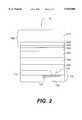
- FIG. 2is a side perspective view of an organic light emitting display device according to another embodiment of the present invention.
- FIG. 3is a side perspective view of an organic light emitting display device according to another embodiment present invention.
- FIG. 4is a side perspective view of an organic light emitting display device according to another embodiment of the present invention.
- FIG. 5is a partial cross sectional view of certain layers of an organic light emitting display according to an embodiment of the present invention.
- FIG. 6is a partial cross sectional view of certain layers of an organic light emitting display according to an embodiment of the present invention.
- FIG. 7is a partial cross sectional view of certain layers of an organic light emitting display according to an embodiment of the present invention.
- FIG. 8is a simplified schematic representation of a matrix layout according to the present invention.
- FIG. 1discloses an organic light emitting device ("OLED") constructed according to the present invention.
- OLED 10 of the present inventionis shown in FIG. 1 and includes a substrate 100. Overlying the substrate 100 is a first conductor 200. Overlying the first conductor 200 is a second conductor 250. Sandwiched between the conductor layers is a layer of light emitting organic material 300. Overlying the conductors and the organic material is a top cover 500. Between the second conductor 250 and the top cover 500 is a microcavity stack 400.
- the substrate 100is substantially planar and underlies and provides support for the entire OLED structure.
- the first and second conductors 200 and 250function as either electron injecting or hole injecting layers. When the positive and negative charges from the conductors meet in the layer of organic material 300, light is emitted.
- OLED 10 of the present inventionmay emit light through either the top cover 500 or the substrate 100.
- the microcavity stack 400functions to restrict light emissions in directions parallel to the substrate 100 and also provides increased light emissions toward the viewer in a direction perpendicular to the substrate.
- the top cover 500is typically transparent and provides sealing and protection for the entire OLED.
- the microcavity stack 400restricts light emissions in directions parallel to the planar substrate 100 and provides increased light emissions toward the viewer.
- the microcavity stack 400minimizes the channelling of light in the organic material 300.
- the microcavity stack 400also directs upward, light which has been emitted in a near Lambertian manner.
- the microcavity stack 400reduces the activation of neighboring pixels, and increases contrast and color purity.
- the microcavity stack 400is located over the organic material 300.
- FIG. 1shows microcavity stack 400 as a discrete layer, it is within the scope of the present invention that the light restricting functions of the stack may be blended into the other elements of the OLED, e.g., the conductor layers.
- the microcavity stack 400may comprise alternating layers of dielectric material deposited on top of one another. Each layer of dielectric material may be chosen for its index of refraction. The thicknesses of each layer of dielectric material may be calculated using formulas commonly available to those skilled in the area. The thickness of each layer depends upon the number and type of layers contained within the microcavity stack 400 and on the types of organic material contained within the light emitting organic material layer 300.
- the microcavity stack 400 and the organic material layer 300combine to narrow the bandwidth of the emitted light. Light emissions may be optimized by the microcavity stack 400 so that the majority of the emitted light falls into the near ultra violet or blue light range of the spectrum. The narrower range of emitted light allows color converters to be more efficient due to their narrower pick-up range.
- the dielectric materialmay be evaporated at shallow angles to the planar substrate 100 in order to minimize pinhole density in the layers.
- An evaporation angle of approximately 30 to 50 degreesis preferred.
- sputter depositingmay also be used to reduce pinhole densities.
- the depositionmay be conducted while the OLED structure is rotating. Shallow angle evaporation and sputter deposition reduce the pinhole density of the microcavity stack 400 below values normally obtained using conventional 90 degree deposition methods.
- Layers of transparent conductormay also be interspersed within the microcavity stack 400. For example, a layer of ITO may be mixed between the layers of dielectric material.
- Zirconium oxide, silicon carbide, silicon oxide, silicon dioxide and lithium flourideare suitable dielectric materials for the layers which comprise the microcavity stack 400.
- the preferred process of depositing the dielectric materialis sputter or ion beam deposition because these processes result in increased densification and large differences of indices of refraction between the dielectric layers. Evaporation or low temperature CVD may also be utilized as alternative processes.
- the use of ion bombardment during deposition of the dielectric materialhas many advantages. For example, ion embodiment allows a single material may be used for the entire microcavity stack 400.
- the stack 400may be comprise alternating layers of densified and undensified dielectric material (e.g. SiO 2 ). Alternatively, transparent conductive material (e.g.
- In 2 O 3may be densified by ion bombardment and interspersed between layers of undensified dielectric material (e.g. ZnO). Ion bombardment also permits thin layers to used within the microcavity stack 400, which may include alternating layers of densified ZrO 2 and undensified SiO 2 .
- undensified dielectric materiale.g. ZnO
- the substrate 100may underlie a plurality of different subpixels or cells 10.
- the substrate 100may be transparent if downward light emission is desired.
- the substrate 100may be a planar thin film transistor array contained on glass (similar to those typically used for TFT-LCD notebook displays).
- the thin film transistor arraymay be placed on foil or ceramic.
- the planar substrate 100may be formed from a silicon integrated circuit wafer.
- the silicon substrate layer 130may comprise integrated circuits 120.
- the integrated circuit 120may be connected to the first conductor 200 by way of a plug or via 140.
- the plug 140is contained within an insulator 110 (e.g. SiO 2 ).
- the via or plug 140may be filled with hot aluminum or tungsten which is chemical vapor deposited ("CVD") and may be planarized with the surrounding insulator using chemical-mechanical polishing ("CMP").
- CVDchemical vapor deposited
- CMPchemical-mechanical polishing
- the planar substrate 100may include the matrix 800, shown in FIG. 8.
- the matrix 800includes matrix lines 801 or 802 which are capable of carrying current or voltage pulses of selected magnitudes.
- the pulsesare provided to the matrix lines 801, 802 by drivers (not shown).
- the signals from the driverspass to the conductors 200, 205 through one the matrix lines 801 and 802, the integrated circuit 120 and the plug 140.
- the signal from the driver current of varying magnitude to the conductorsthereby determining whether or not each OLED or pixel cell, is on, off or at some intermediate gray level.
- the matrix address lines 801, 802may be sequenced so that light emissions are constantly changing. The viewer's eye integrates the emitted light to see images.
- the driversare optimally built into the substrate 100 in order to save space and to minimize the number of connections. However, the drivers may be connected to the perimeter of the substrate 100 using TAB automated bonding or other well known techniques. The drivers may provide merely on/off signals for some applications such as word processing or spreadsheet. However, most software relies heavily upon different gray levels for providing additional information to the viewer, and therefore the drivers must provide pulses of various magnitudes.
- the driversgenerate coded pulses for the active matrix 800.
- the pulsesmay be coded using either amplitude or pulse width modulation.
- pulse width modulationis preferred because the sharpness of the transfer function limits the use of other methods.
- the pulse width modulated signaloperates on a time slice basis, where the gray level is proportional to the amount of time the signal is applied to the subpixels or cells. Pulse width modulation is largely insensitive to the nonuniformities between different cells or OLEDs on the matrix. This insensitivity is a result of the signal switching between the two extreme points on the response curve. As a result, the use of a pulse width modulated driver signal reduces uniformity requirements and increases yield.
- each OLED 10include within its circuitry 120 a pair of transistors and a capacitor in order to achieve this end, although there are many acceptable substrate circuit designs. Normally, the image is presented to the viewer at all times except for during the brief period when a cell is being refreshed. In addition to improving OLED brightness, the refreshing process improves the OLED image retention inmmunity.
- FIG. 3discloses the first conductor 200 which may serve as either the cathode or anode.
- the first conductor 200may be formed from materials such as MoSI 2 , WSI 2 , Mo, Al, or aluminum alloys such as Al-2% Cu or Al+5% Ti.
- the first conductor 200includes a conductor pad 202 which may be planarized with a surrounding dielectric 201. Silicon dioxide is a preferred material for the dielectric 201. Prior to planarization the conductor pad 202 is formed thicker than required. A 500 mn amount of conductor is deposited followed by the deposition of 1,000 nm of silicon dioxide. The combined surface is chemically mechanically polished in order to leave a planar surface of mixed conductor and dielectric. The use of planarized conductor pads avoids edge steps which can result in thinning of the organic materials, and breakdown failures or broken conductors during fabrication.
- the first conductor 200comprises a conductor pad 202 with tapered side walls of at least 30 degrees or even more.
- the sloped conductor pad 202is surrounded by a transition layer 203 capable of injecting holes or electrons.
- the transition layer 203may comprise barium titanate or other high dielectric constant materials.
- the transition layer 203may also comprise a dielectric material comprising 5 to 60 percent Cr and SiO with or without low work function contaminants comprising alkali or alkaline metals such as Cs, Mg, Ba, Sc or Li or alloys or mixtures of these materials.
- the transition layermay also comprise other organic or inorganic injector materials such as CuPC.
- the slope of the pad 202is achieved by undercutting the edges.
- the undercuttingis achieved through resist or bilayer adhesion loss. Alternatively, the undercutting may be achieved by resist edge ablation during RIE.
- the first conductor 200may include both the transition layer 203 and dielectric layer 201.
- injection enhancement layer(not shown) comprising Al+Li, Mg+Ag, or Pd, Pt or Au may be included over the transition barrier 203. The injection enhancement layer improves the injection of holes or electrons into the organic material 300.
- FIG. 5discloses the layer of light emitting organic material 300 which comprises three layers 310, 320 and 330.
- the arrangement of the layersis determined by the direction of electron injection into organic layer stack 300.
- layer 330is preferentially Perylene doped BAlq
- layer 320is preferentially NPB
- layer 310is CuPc.
- the preferred thicknesses for the CuPc, NPB and Perylene doped BAlq layersare 15 nm, 60 nm, and 70 nm, respectively.
- the Perylene doped BAlq layerproduces blue light. Blue to ultraviolet light is preferred to obtain full color displays using color conversion.
- White emitterscan be obtained from either dysprosium dopant or a mixed layer emitter. Other colors, such as green or white on black, may also be used for monochrome or multicolored displays. As an alternative, the layer of light emitting organic material 300 may be comprise a single blended layer rather than separate distinct layers.
- the second conductor 250Overlying the light emitting organic material 300 is the second conductor 250.
- the second conductor 250includes a conductor layer 251 and a transition layer 253.
- the transition layer 253is preferentially formed from either LiF or barium and has a thickness of approximately 10 nms. In order to simplify fabrication, transition layers 253 and 203 are generally composed of identical materials.
- the conductor layer 251is formed by depositing ITO to a thickness of approximately 150 nms using long throw distance S-gun sputtering. The S-gun sputter deposition process will close off pinholes in the conductor layer. Shadow masks commonly used in the electronics industry may also be used to keep the transparent conductors from depositing on and shorting out exposed leads near the perimeter of the display.
- An optional getter layer 252may be located between the conductor layer 251 and the transition layer 253.
- the getter layer 252preferentially comprises alternating layers of zinc oxide and aluminum of approximately 1 nm each.
- the layers which make up the getter layer 252are preferentially evaporated at shallow angles (e.g. 30 degrees). Pinholes in the getter layer 252 may be reduced by the shallow angle evaporation.
- Top cover 500Overlying the second conductor 250 is the top cover 500.
- Top cover 500includes a protective cover glass 510, a color converter layer 520, and a barrier layer 540.
- the transparent cover glass 510preferentially is formed from silicon and has a thickness of approximately 0.2 mm thick.
- the cover glass 510may overly the entire matrix 800.
- a barrier layer 540overlies the microcavity stack 400.
- the barrier layer 540comprises a layer of diamond-like amorphous carbon ("DLC") or silicon carbide (SiC), or in the case of top injecting OLEDs a cesium doped diamond-like carbide composition (CsC approximately 10% Cs and 90% C by molar ratio).
- DLCis a film consisting of amorphous carbon, which may include hydrogen, that is transparent and has a high refractive index (>2). Such films are typically deposited by laser ablation from graphite or plasma enhanced CVD from a gas such as methane with a small amount of oxygen.
- the barrier layer 540acts a barrier to residual moisture within the OLED.
- the barrier layer 540may also serve as a heat sink for heat generated during light emission.
- the barrier layermay also serve as a hole or electron injector. When functioning as an injector the barrier layer 540 is typically doped with Lithium or Palladium for electron or hole injection respectively.
- the barrier layer 540underlies a sealing layer 530 and overlies the *microcavity stack 400.
- the barrier layer 540may be formed using either shallow evaporation or Plasma Enhanced Chemical Vapor Deposition ("PECVD").
- PECVDPlasma Enhanced Chemical Vapor Deposition
- the PECVD processmay include, for example, inductively coupled plasma using a methane and diluted CF 4 source plus an argon source.
- Transparent inductively coupled plasma DLC filmshave low pinhole density and a high index of refraction making them easy to use when mutually combined with PECVD evaporated or sputter deposited silicon dioxide layers. Silicon carbide formed from PECVD or evaporation may be used in lieu of the DLC high index of refraction layers.
- the barrier layer 540may comprise an upper DLC layer 541 and a lower DLC layer 542. Multiple layers of getter material 545 and 546 may be formed within the top layer 541.
- the getter material layersmay be formed from calcium, magnesium, titanium or aluminum in alternation with DLC or other dielectric materials S 3 N 4 , SiO or SiO 2 .
- a transparent conductor such as ZnOmay be used in place of the transparent dielectric material in order to provide added conductivity. While, the structure and materials set forth above are preferred, the invention includes the use of getter layer comprising any transparent material capable of removing moisture.
- a sealing layer 530may be included between the barrier layer 540 and the color converter layer 520.
- the sealing layer 530hermetically seals the OLED in order to protect the device from oxygen and moisture.
- the sealing layer 530is typically formed from a commercially available heat sink gel material. The gel material may be dried extensively by heating in a high vacuum or by mixing in a desiccant such as BaO. As an alternative, an ultraviolet light cured epoxy, e.g. Acrylate, may be used. Solvent containing adhesives are not recommended unless a totally pinhole free cover layer is produced.
- the sealing layer 530may further comprise a mixture of chemically active materials such as fmely powdered aluminum, calcium, magnesium or titanium for moisture removal. Hermetic metal seals may also serve as the sealing layer 530. These metal seals are commonly used for hermetically packaging electronic equipment.
- the sealing layer 530may cover a plurality of OLEDs contained within a display.
- the sealing layer 530is applied uniformly across the display to ensure no oxygen or moisture is trapped within the display.
- the sealing layer 530is preferentially formed in a vacuum environment. If a vacuum environment is not available, the sealing layer 530 may be formed in an inert gas environment such as nitrogen or argon. Adhesion in the sealing layer 530 may be induced by selection of the proper sealing conditions. For example, exposing a display, fabricated according to the present invention, to a temperature of 100° C. and a pressure of 50 psi will normally induce adhesion between the sealing gel and the surrounding layers. If the OLED is sealed in a vacuum, the resulting gap may be eliminated when air pressure is returned to the exterior of the OLED.
- the sealing layer 530may include a heat adhesive perimeter seal (not shown).
- the perimeter sealmay be used alone or in conjunction with the sealing layer 530 which extends across the entire display. Getter material such as finely divided Mg, Ba, Ca, Al or Ti may be mixed into the perimeter seal for additional vapor collection.
- the perimeter sealtypically comprises an ultraviolet light cured epoxy.
- the color converter layer 520may be formed by providing color conversion dye materials above the barrier layer 540.
- the color conversion dye materialswork with an OLED emitter that emits short wave length lights, for example blue, near ultraviolet, or ultraviolet.
- the dye materialsgenerally comprise PPV based compounds or other fluorescent materials and are commercially available from many sources including, for example, Idemitsu Kosan Corporation.
- the dye materialsabsorb the short wave length flight and re-emit or fluoresce longer wave length flight in characteristic colors such as red or green.
- These color conversion dye materialsmay be selected and patterned on the cover glass 510 using conventional lithographic means.
- the dye materialsmay be used to create a full color CRT-like display with red, green and blue pixels.
- the varying grey levels available from the perimeter drivers and the active matrixmay be used to create intensity mixtures of three primary colors and result in TV-like images.
- Blue converter dye materialmay be used if near-ultraviolet light emitting layers are used.
- Full color displaysmay be displayed using color filters in lieu of converter dye material.
- the color filtermay be used with a white light emitting organic layer 300. Blue light emitting organic material may be used with or without color filters.
- a further embodiment of the color converter layer 520utilizes commercially available color wheels or pi-cells for color conversion. All of these techniques are commonly known in the industry.
- the present inventionalso includes the use of black matrix or reflective metal trenches 803 surrounding each subpixel or OLED 10.
- the black matrix or reflective metal trenches 803, shown in FIG. 8,help to minimize channeling in the small pitch pixels and improve color purity.
- the black matrixpreferably comprises a mixture of co-evaporated 40 to 80% chromium and silicon oxide. If the OLED is to be used in a head wearable application, e.g. medical imaging, night vision, or virtual reality applications, it is preferred to use chromium or aluminum reflective barriers. The chromium or aluminum barriers may provide more light output while at the same time controlling channeling.
Landscapes
- Physics & Mathematics (AREA)
- Optics & Photonics (AREA)
- Electroluminescent Light Sources (AREA)
Abstract
Description
Claims (24)
Priority Applications (9)
| Application Number | Priority Date | Filing Date | Title |
|---|---|---|---|
| US09/074,424US5920080A (en) | 1997-06-23 | 1998-05-08 | Emissive display using organic light emitting diodes |
| CNB988075989ACN100336240C (en) | 1997-06-23 | 1998-06-18 | Emissive display using organic light emitting diodes |
| JP50479799AJP2002508108A (en) | 1997-06-23 | 1998-06-18 | Light emitting display using organic light emitting diode |
| PCT/US1998/012694WO1998059528A1 (en) | 1997-06-23 | 1998-06-18 | Emissive display using organic light emitting diodes |
| CA002294279ACA2294279A1 (en) | 1997-06-23 | 1998-06-18 | Emissive display using organic light emitting diodes |
| EP98930369AEP1016327A1 (en) | 1997-06-23 | 1998-06-18 | Emissive display using organic light emitting diodes |
| KR1019997012208AKR20010020501A (en) | 1997-06-23 | 1998-06-18 | Emissive display using organic light emitting diodes |
| IL13367898AIL133678A0 (en) | 1997-06-23 | 1998-06-18 | Emissive display using organic light emitting diodes |
| IL133678AIL133678A (en) | 1997-06-23 | 1999-12-23 | Emissive display using organic light emitting diodes |
Applications Claiming Priority (2)
| Application Number | Priority Date | Filing Date | Title |
|---|---|---|---|
| US5045997P | 1997-06-23 | 1997-06-23 | |
| US09/074,424US5920080A (en) | 1997-06-23 | 1998-05-08 | Emissive display using organic light emitting diodes |
Publications (1)
| Publication Number | Publication Date |
|---|---|
| US5920080Atrue US5920080A (en) | 1999-07-06 |
Family
ID=26728294
Family Applications (1)
| Application Number | Title | Priority Date | Filing Date |
|---|---|---|---|
| US09/074,424Expired - LifetimeUS5920080A (en) | 1997-06-23 | 1998-05-08 | Emissive display using organic light emitting diodes |
Country Status (8)
| Country | Link |
|---|---|
| US (1) | US5920080A (en) |
| EP (1) | EP1016327A1 (en) |
| JP (1) | JP2002508108A (en) |
| KR (1) | KR20010020501A (en) |
| CN (1) | CN100336240C (en) |
| CA (1) | CA2294279A1 (en) |
| IL (2) | IL133678A0 (en) |
| WO (1) | WO1998059528A1 (en) |
Cited By (143)
| Publication number | Priority date | Publication date | Assignee | Title |
|---|---|---|---|---|
| WO2000012226A1 (en)* | 1998-08-28 | 2000-03-09 | Fed Corporation | Full color organic light emitting diode display and method for making the same using inkjet fabrication |
| US6064151A (en)* | 1997-12-08 | 2000-05-16 | Motorola, Inc. | Organic electroluminescent device with enhanced performance |
| US6133692A (en)* | 1998-06-08 | 2000-10-17 | Motorola, Inc. | White light generating organic electroluminescent device and method of fabrication |
| US6133693A (en)* | 1998-07-30 | 2000-10-17 | Alliedsignal Inc. | Interconnects and electrodes for high luminance emissive displays |
| WO2001015244A1 (en)* | 1999-08-20 | 2001-03-01 | Emagin Corporation | Organic light emitting diode device with high work function metal-oxide anode layer and method of fabrication of same |
| US6281634B1 (en)* | 1998-12-01 | 2001-08-28 | Sanyo Electric Co., Ltd. | Color electroluminescence display device |
| US20010023661A1 (en)* | 2000-02-04 | 2001-09-27 | Semiconductor Energy Laboratory Co., Ltd. | Thin film formation apparatus and method of manufacturing self-light-emitting device using thin film formation apparatus |
| US20010035713A1 (en)* | 2000-04-21 | 2001-11-01 | Semiconductor Energy Laboratory Co., Ltd. | Self-light emitting device and electrical appliance using the same |
| US6351036B1 (en)* | 1998-08-20 | 2002-02-26 | The United States Of America As Represented By The Secretary Of The Navy | Electronic devices with a barrier film and process for making same |
| US20020025675A1 (en)* | 2000-05-03 | 2002-02-28 | Chu Tak Kin | Electronic devices with diffusion barrier and process for making same |
| US20020030443A1 (en)* | 2000-09-08 | 2002-03-14 | Toshimitsu Konuma | Light emitting device, method of manufacturing the same, and thin film forming apparatus |
| US6429599B1 (en) | 1998-12-01 | 2002-08-06 | Sanyo Electric Co., Ltd. | Color electroluminescence display device |
| US6433486B1 (en) | 1998-12-01 | 2002-08-13 | Sanyo Electric Co., Ltd. | Color electroluminescence display device |
| WO2002079690A1 (en)* | 2001-03-30 | 2002-10-10 | Candescent Intellectual Property Services, Inc. | Structure and fabrication of light-emitting device having light-reflective layer formed with, or/and adjacent to, material that enhances device performance |
| US6465953B1 (en)* | 2000-06-12 | 2002-10-15 | General Electric Company | Plastic substrates with improved barrier properties for devices sensitive to water and/or oxygen, such as organic electroluminescent devices |
| WO2003001853A1 (en)* | 2001-06-22 | 2003-01-03 | University Of Cincinnati | Light emissive display with a black or color dielectric layer |
| US20030022409A1 (en)* | 2001-07-27 | 2003-01-30 | The Ohio State University | Methods for fabricating polymer light emitting devices by lamination |
| US6525758B2 (en) | 2000-12-28 | 2003-02-25 | Polaroid Corporation | Integral organic light emitting diode fiber optic printhead utilizing color filters |
| US20030062518A1 (en)* | 1999-12-17 | 2003-04-03 | Mark Auch | Method for encapsulation of electronic devices |
| US6545422B1 (en) | 2000-10-27 | 2003-04-08 | Science Applications International Corporation | Socket for use with a micro-component in a light-emitting panel |
| US6552488B1 (en) | 1999-08-24 | 2003-04-22 | Agilent Technologies, Inc. | Organic electroluminescent device |
| US20030085652A1 (en)* | 2001-11-06 | 2003-05-08 | Weaver Michael Stuart | Encapsulation structure that acts as a multilayer mirror |
| US20030094691A1 (en)* | 1999-12-17 | 2003-05-22 | Mark Auch | Encapsulation of electronic devices |
| US6570335B1 (en) | 2000-10-27 | 2003-05-27 | Science Applications International Corporation | Method and system for energizing a micro-component in a light-emitting panel |
| WO2003045865A1 (en)* | 2001-11-21 | 2003-06-05 | Optical Coating Laboratory, Inc. | Glass panel with barrier coating and related methods |
| US6579237B1 (en) | 2001-12-14 | 2003-06-17 | Koninklijke Philips Electronics Nv | Diagnostic ultrasonic imaging system having organic light emitting device display |
| US6590337B1 (en)* | 1999-09-29 | 2003-07-08 | Sanyo Electric Co., Ltd. | Sealing structure for display device |
| US6606110B2 (en) | 2000-12-27 | 2003-08-12 | Polaroid Corporation | Integral organic light emitting diode printhead |
| US6612889B1 (en) | 2000-10-27 | 2003-09-02 | Science Applications International Corporation | Method for making a light-emitting panel |
| US6617052B2 (en)* | 2000-03-21 | 2003-09-09 | Seiko Epson Corporation | Organic EL element and method of manufacturing the same |
| US6620012B1 (en) | 2000-10-27 | 2003-09-16 | Science Applications International Corporation | Method for testing a light-emitting panel and the components therein |
| US20030173895A1 (en)* | 2002-01-31 | 2003-09-18 | Yoshifumi Kato | Organic electroluminescent color display unit |
| US6624839B2 (en) | 2000-12-20 | 2003-09-23 | Polaroid Corporation | Integral organic light emitting diode printhead utilizing color filters |
| US20030184221A1 (en)* | 2002-03-28 | 2003-10-02 | Masayuki Mishima | Light-emitting device |
| US6639250B1 (en) | 1999-08-20 | 2003-10-28 | Seiko Epson Corporation | Multiple-wavelength light emitting device and electronic apparatus |
| US20030201445A1 (en)* | 2002-04-25 | 2003-10-30 | Lg.Philips Lcd Co., Ltd. | Organic electroluminescent display device |
| US20030207645A1 (en)* | 2000-10-27 | 2003-11-06 | George E. Victor | Use of printing and other technology for micro-component placement |
| US20030207643A1 (en)* | 2000-10-27 | 2003-11-06 | Wyeth N. Convers | Method for on-line testing of a light emitting panel |
| US20030207644A1 (en)* | 2000-10-27 | 2003-11-06 | Green Albert M. | Liquid manufacturing processes for panel layer fabrication |
| US20030214243A1 (en)* | 2000-10-27 | 2003-11-20 | Drobot Adam T. | Method and apparatus for addressing micro-components in a plasma display panel |
| US20030214230A1 (en)* | 2002-05-03 | 2003-11-20 | Wood Richard P. | Dark layer for an electroluminescent device |
| US20040000864A1 (en)* | 2002-06-27 | 2004-01-01 | Yoshifumi Kato | Color display unit |
| US20040004436A1 (en)* | 2002-05-24 | 2004-01-08 | Sanyo Electric Co., Ltd. | Electroluminescent display device |
| US20040018305A1 (en)* | 2002-04-15 | 2004-01-29 | Pagano John Chris | Apparatus for depositing a multilayer coating on discrete sheets |
| US20040031977A1 (en)* | 2002-04-12 | 2004-02-19 | Brown Julia J. | Protected organic electronic devices and methods for making the same |
| US20040043251A1 (en)* | 1996-08-02 | 2004-03-04 | Epstein Arthur J. | Electroluminescence in light emitting polymers featuring deaggregated polymers |
| US20040046165A1 (en)* | 2000-09-11 | 2004-03-11 | Arvid Hunze | Plasma encapsulation for electronic and microelectronic components such as oleds |
| US6713955B1 (en)* | 1998-11-20 | 2004-03-30 | Agilent Technologies, Inc. | Organic light emitting device having a current self-limiting structure |
| US6720654B2 (en)* | 1998-08-20 | 2004-04-13 | The United States Of America As Represented By The Secretary Of The Navy | Electronic devices with cesium barrier film and process for making same |
| US20040087252A1 (en)* | 2002-10-30 | 2004-05-06 | Yan-Ming Huang | Method for manufacturing organic light emitting diode with improved electrical leakage |
| US6737753B2 (en)* | 2001-09-28 | 2004-05-18 | Osram Opto Semiconductor Gmbh | Barrier stack |
| US6737176B1 (en)* | 1999-07-15 | 2004-05-18 | Nec Corporation | Organic electroluminescent device and method for fabricating same |
| US20040108811A1 (en)* | 2002-09-11 | 2004-06-10 | Hagen Klausmann | OLED Devices with Improved Encapsulation |
| US6763167B2 (en) | 2000-12-20 | 2004-07-13 | Polaroid Corporation | Integral organic light emitting diode fiber optic printhead |
| US6762566B1 (en) | 2000-10-27 | 2004-07-13 | Science Applications International Corporation | Micro-component for use in a light-emitting panel |
| US20040164292A1 (en)* | 2003-02-21 | 2004-08-26 | Yeh-Jiun Tung | Transflective display having an OLED backlight |
| US6790594B1 (en)* | 2003-03-20 | 2004-09-14 | Eastman Kodak Company | High absorption donor substrate coatable with organic layer(s) transferrable in response to incident laser light |
| US20040206953A1 (en)* | 2003-04-16 | 2004-10-21 | Robert Morena | Hermetically sealed glass package and method of fabrication |
| US20040207314A1 (en)* | 2003-04-16 | 2004-10-21 | Aitken Bruce G. | Glass package that is hermetically sealed with a frit and method of fabrication |
| US6822626B2 (en) | 2000-10-27 | 2004-11-23 | Science Applications International Corporation | Design, fabrication, testing, and conditioning of micro-components for use in a light-emitting panel |
| US6835950B2 (en)* | 2002-04-12 | 2004-12-28 | Universal Display Corporation | Organic electronic devices with pressure sensitive adhesive layer |
| US20050007306A1 (en)* | 2003-05-29 | 2005-01-13 | Seiko Epson Corporation | Display device and projection display device |
| US20050012445A1 (en)* | 1999-10-12 | 2005-01-20 | Shunpei Yamazaki | EL display device and a method of manufacturing the same |
| US20050023976A1 (en)* | 2003-07-07 | 2005-02-03 | Yuxin Wang | Seal and sealing process for electroluminescent displays |
| US20050045900A1 (en)* | 2003-08-25 | 2005-03-03 | Universal Display Corporation | Protected organic electronic device structures incorporating pressure sensitive adhesive and desiccant |
| US20050067718A1 (en)* | 2003-09-25 | 2005-03-31 | Osram Opto Semiconductors Gmbh | Transport balancing diffusion layer for rate limited scavenging systems |
| US20050077615A1 (en)* | 2003-10-10 | 2005-04-14 | Gang Yu | Heat sinks |
| US6885147B2 (en)* | 1998-05-18 | 2005-04-26 | Emagin Corporation | Organic light emitting diode devices with improved anode stability |
| US20050095452A1 (en)* | 2003-11-04 | 2005-05-05 | Eastman Kodak Company | Organic element for electroluminescent devices |
| WO2005048367A1 (en)* | 2003-11-13 | 2005-05-26 | Philips Intellectual Property & Standards Gmbh | Electronic device comprising a protective barrier layer stack |
| US20050109282A1 (en)* | 2003-11-25 | 2005-05-26 | Liya Regel | Method for manufacturing diamond coatings |
| US20050116621A1 (en)* | 2003-11-18 | 2005-06-02 | Erika Bellmann | Electroluminescent devices and methods of making electroluminescent devices including a color conversion element |
| US20050136571A1 (en)* | 1999-07-09 | 2005-06-23 | Osram Gmbh, A German Corporation | Encapsulating a device |
| US20050151151A1 (en)* | 2003-04-16 | 2005-07-14 | Hawtof Daniel W. | Hermetically sealed package and method of fabrication of a hermetically sealed package |
| US20050189164A1 (en)* | 2004-02-26 | 2005-09-01 | Chang Chi L. | Speaker enclosure having outer flared tube |
| US20050227387A1 (en)* | 2004-02-26 | 2005-10-13 | Eastman Kodak Company | Bonding a cover plate over encapsulated OLEDs |
| US20050230687A1 (en)* | 2002-12-12 | 2005-10-20 | Toshihiko Ushiro | Light-emitting device having a diffractive optical film on light emission surface and method for manufacturing same |
| US20050236640A1 (en)* | 1999-07-09 | 2005-10-27 | Osram Opto Semiconductors GmbH & CO. OHG, a German corporation | Laminates for encapsulating devices |
| US20050238803A1 (en)* | 2003-11-12 | 2005-10-27 | Tremel James D | Method for adhering getter material to a surface for use in electronic devices |
| US6960877B1 (en)* | 1998-12-17 | 2005-11-01 | Cambrdige Display Technology Limited | Organic light-emitting devices including specific barrier layers |
| US6965361B1 (en)* | 1998-06-16 | 2005-11-15 | Agilent Technologies, Inc. | Method of manufacture of active matrix addressed polymer LED display |
| US20050269943A1 (en)* | 2004-06-04 | 2005-12-08 | Michael Hack | Protected organic electronic devices and methods for making the same |
| US20050280008A1 (en)* | 2004-06-16 | 2005-12-22 | Eastman Kodak Company | Array of light-emitting oled microcavity pixels |
| US20060003487A1 (en)* | 2004-06-30 | 2006-01-05 | Intel Corporation | Low power consumption OLED material for display applications |
| US20060008580A1 (en)* | 2000-11-24 | 2006-01-12 | Gabrielle Nelles | Hybrid solar cells with thermal deposited semiconductive oxide layer |
| US20060017379A1 (en)* | 2004-07-23 | 2006-01-26 | Au Optronics Corp. | Dual-sided display |
| US20060017055A1 (en)* | 2004-07-23 | 2006-01-26 | Eastman Kodak Company | Method for manufacturing a display device with low temperature diamond coatings |
| US7001060B1 (en) | 1999-08-11 | 2006-02-21 | Semiconductor Energy Laboratory Co., Ltd. | Front light having a plurality of prism-shaped lenses |
| US7005196B1 (en)* | 1998-12-16 | 2006-02-28 | Cambridge Display Technology Limited | Organic light-emitting devices |
| US20060086020A1 (en)* | 2004-10-27 | 2006-04-27 | Eastman Kodak Company | Multi-mode flat-panel light-emitting sign |
| US20060093795A1 (en)* | 2004-11-04 | 2006-05-04 | Eastman Kodak Company | Polymeric substrate having a desiccant layer |
| US20060099446A1 (en)* | 2004-11-06 | 2006-05-11 | Young-Hun Byun | Cyclometalated transition metal complex and organic electroluminescent display device using the same |
| US20060097264A1 (en)* | 2004-11-10 | 2006-05-11 | Samsung Sdi Co., Ltd. | Light-emitting device having optical resonance layer |
| US20060097630A1 (en)* | 2004-11-10 | 2006-05-11 | Pentax Corporation | Organic electroluminescent device and process for producing this same |
| US20060125734A1 (en)* | 2004-12-09 | 2006-06-15 | Eastman Kodak Company | OLED display with aging compensation |
| US20060158101A1 (en)* | 2003-03-04 | 2006-07-20 | Dow Corning Corporation | Organic light-emitting diode |
| US20060267485A1 (en)* | 2002-11-13 | 2006-11-30 | Wood Richard P | Organic light emitting diode (oled) with contrast enhancement features |
| US20060281953A1 (en)* | 2003-01-17 | 2006-12-14 | Hans-Helmut Bechtel | Recovery of an active catalyst component from a process stream |
| US20060283546A1 (en)* | 2003-11-12 | 2006-12-21 | Tremel James D | Method for encapsulating electronic devices and a sealing assembly for the electronic devices |
| US20060284556A1 (en)* | 2003-11-12 | 2006-12-21 | Tremel James D | Electronic devices and a method for encapsulating electronic devices |
| US20070046213A1 (en)* | 2002-09-30 | 2007-03-01 | Kenji Nakamura | Organic el laminate type organic switching element and organic el display |
| US20070049155A1 (en)* | 2005-08-25 | 2007-03-01 | Vitex Systems, Inc. | Encapsulated devices and method of making |
| US7198832B2 (en) | 1999-10-25 | 2007-04-03 | Vitex Systems, Inc. | Method for edge sealing barrier films |
| US20070103069A1 (en)* | 2005-11-02 | 2007-05-10 | Ifire Technology Corp. | Laminated conformal seal for electroluminescent displays |
| US20070200794A1 (en)* | 1996-06-14 | 2007-08-30 | 3M Innovative Properties Company | Display unit and methods of displaying an image |
| US7288014B1 (en) | 2000-10-27 | 2007-10-30 | Science Applications International Corporation | Design, fabrication, testing, and conditioning of micro-components for use in a light-emitting panel |
| US20080053525A1 (en)* | 2000-11-24 | 2008-03-06 | Sony Deutschland Gmbh | Hybrid solar cells with thermal deposited semiconductive oxide layer |
| US20080124558A1 (en)* | 2006-08-18 | 2008-05-29 | Heather Debra Boek | Boro-silicate glass frits for hermetic sealing of light emitting device displays |
| EP1154676A4 (en)* | 1999-11-22 | 2008-08-20 | Sony Corp | DISPLAY DEVICE |
| US20080211390A1 (en)* | 2007-03-02 | 2008-09-04 | D Andrade Brian | Organic light emitting device having an external microcavity |
| USRE40531E1 (en) | 1999-10-25 | 2008-10-07 | Battelle Memorial Institute | Ultrabarrier substrates |
| US7494837B2 (en) | 1999-10-13 | 2009-02-24 | Semiconductor Energy Laboratory Co., Ltd. | Thin film forming apparatus |
| US20090058268A1 (en)* | 2005-09-29 | 2009-03-05 | Matsushita Electric Industrial Co., Ltd. | Organic el display and method for manufacturing same |
| US7510913B2 (en) | 2003-04-11 | 2009-03-31 | Vitex Systems, Inc. | Method of making an encapsulated plasma sensitive device |
| USRE40787E1 (en) | 1999-10-25 | 2009-06-23 | Battelle Memorial Institute | Multilayer plastic substrates |
| US20090169770A1 (en)* | 2005-07-20 | 2009-07-02 | 3M Innovative Properties Company | Moisture barrier coatings |
| US20090252894A1 (en)* | 2006-06-19 | 2009-10-08 | 3M Innovative Properties Company | Moisture barrier coatings for organic light emitting diode devices |
| US7648925B2 (en) | 2003-04-11 | 2010-01-19 | Vitex Systems, Inc. | Multilayer barrier stacks and methods of making multilayer barrier stacks |
| US20100051965A1 (en)* | 2008-08-29 | 2010-03-04 | Chen-Hua Yu | Carbon-Containing Semiconductor Substrate |
| US7786958B1 (en) | 1999-09-24 | 2010-08-31 | Semiconductor Energy Laboratory Co., Ltd. | EL display device and electronic device |
| US20110008525A1 (en)* | 2009-07-10 | 2011-01-13 | General Electric Company | Condensation and curing of materials within a coating system |
| US20110025196A1 (en)* | 2009-07-31 | 2011-02-03 | General Electric Company | Hermetic package with getter materials |
| US8097922B1 (en)* | 2007-05-29 | 2012-01-17 | The Regents Of The University Of California | Nanometer-scale transistor architecture providing enhanced carrier mobility |
| US20120080669A1 (en)* | 2002-06-11 | 2012-04-05 | Semiconductor Energy Laboratory Co., Ltd. | Light emitting device and manufacturing method thereof |
| US8183571B2 (en) | 1999-09-17 | 2012-05-22 | Semiconductor Energy Laboratory Co., Ltd. | EL display device and method for manufacturing the same |
| US8198203B2 (en) | 2008-10-20 | 2012-06-12 | Corning Incorporated | Antimony-free glass, antimony-free frit and a glass package that is hermetically sealed with the frit |
| WO2012152812A1 (en)* | 2011-05-10 | 2012-11-15 | Basf Se | Novel color converters |
| US8383455B2 (en) | 2005-12-23 | 2013-02-26 | E I Du Pont De Nemours And Company | Electronic device including an organic active layer and process for forming the electronic device |
| US8590338B2 (en) | 2009-12-31 | 2013-11-26 | Samsung Mobile Display Co., Ltd. | Evaporator with internal restriction |
| US8624134B2 (en) | 2010-07-29 | 2014-01-07 | Industrial Technology Research Institute | Package of environmental sensitive element and encapsulation method of the same |
| US8629439B2 (en) | 2002-01-24 | 2014-01-14 | Semiconductor Energy Laboratory Co., Ltd. | Light emitting device, method of preparing the same and device for fabricating the same |
| US20140306200A1 (en)* | 2013-04-11 | 2014-10-16 | Sony Corporation | Display unit and electronic apparatus |
| US8900366B2 (en) | 2002-04-15 | 2014-12-02 | Samsung Display Co., Ltd. | Apparatus for depositing a multilayer coating on discrete sheets |
| US8955217B2 (en) | 1999-10-25 | 2015-02-17 | Samsung Display Co., Ltd. | Method for edge sealing barrier films |
| US9184410B2 (en) | 2008-12-22 | 2015-11-10 | Samsung Display Co., Ltd. | Encapsulated white OLEDs having enhanced optical output |
| US9337446B2 (en) | 2008-12-22 | 2016-05-10 | Samsung Display Co., Ltd. | Encapsulated RGB OLEDs having enhanced optical output |
| US20170115521A1 (en)* | 2009-08-13 | 2017-04-27 | 3M Innovative Properties Company | Conducting film or electrode with improved optical and electrical performance for display and lighting devices and solar cells |
| US9639064B2 (en) | 2015-09-18 | 2017-05-02 | Timex Group Usa, Inc. | Wearable electronic device with hand synchronization |
| US9691828B2 (en) | 2014-04-15 | 2017-06-27 | Boe Technology Group Co., Ltd. | Display apparatus having thin films including nanoparticles |
| CN111584693A (en)* | 2020-05-22 | 2020-08-25 | 佛山市国星半导体技术有限公司 | A kind of high reliability LED chip and its manufacturing method |
| US20210066416A1 (en)* | 2019-08-30 | 2021-03-04 | Boe Technology Group Co., Ltd. | Display Substrate and Preparation Method Thereof, and Display Device |
| US10950821B2 (en) | 2007-01-26 | 2021-03-16 | Samsung Display Co., Ltd. | Method of encapsulating an environmentally sensitive device |
| US11758751B2 (en) | 2020-06-22 | 2023-09-12 | Emagin Corporation | Display comprising OLEDs having transparent top electrodes and method of forming same |
Families Citing this family (22)
| Publication number | Priority date | Publication date | Assignee | Title |
|---|---|---|---|---|
| US6140764A (en)* | 1998-07-20 | 2000-10-31 | Motorola, Inc. | Organic electroluminescent apparatus with mircrocavity |
| GB2351840A (en) | 1999-06-02 | 2001-01-10 | Seiko Epson Corp | Multicolour light emitting devices. |
| US6366017B1 (en) | 1999-07-14 | 2002-04-02 | Agilent Technologies, Inc/ | Organic light emitting diodes with distributed bragg reflector |
| JP4759719B2 (en)* | 2000-02-01 | 2011-08-31 | モトローラ ソリューションズ インコーポレイテッド | Light emitting device and manufacturing method |
| DE60031641T2 (en)* | 2000-02-09 | 2007-11-08 | Motorola, Inc., Schaumburg | Electroluminescent device and manufacturing process |
| US7255823B1 (en) | 2000-09-06 | 2007-08-14 | Institute Of Materials Research And Engineering | Encapsulation for oled devices |
| JP3508741B2 (en)* | 2001-06-05 | 2004-03-22 | ソニー株式会社 | Display element |
| JP2003288983A (en)* | 2002-01-24 | 2003-10-10 | Semiconductor Energy Lab Co Ltd | Light emitting device, method for preparing and manufacturing the device |
| NL1020635C2 (en)* | 2002-05-21 | 2003-11-24 | Otb Group Bv | Method for manufacturing a polymeric OLED. |
| KR20030093515A (en)* | 2002-06-03 | 2003-12-11 | 주식회사 엘지화학 | Organic light emitting devices contained hologram collimator film |
| TWI272866B (en)* | 2002-10-16 | 2007-02-01 | Idemitsu Kosan Co | Organic electroluminescent display and method for manufacturing same |
| KR100515827B1 (en)* | 2002-10-28 | 2005-09-21 | 삼성에스디아이 주식회사 | Organic electroluminescence device |
| US6853133B2 (en)* | 2003-05-07 | 2005-02-08 | Eastman Kodak Company | Providing an emission-protecting layer in an OLED device |
| KR100683737B1 (en)* | 2004-12-13 | 2007-02-15 | 삼성에스디아이 주식회사 | Electroluminescent display device |
| US20070013293A1 (en)* | 2005-07-12 | 2007-01-18 | Eastman Kodak Company | OLED device having spacers |
| US20070164673A1 (en)* | 2006-01-18 | 2007-07-19 | Au Optronics Corporation | Organic electro-luminescent display device and method for making same |
| KR100739650B1 (en)* | 2006-08-25 | 2007-07-13 | 삼성에스디아이 주식회사 | OLED display and manufacturing method thereof |
| US7855508B2 (en)* | 2007-09-17 | 2010-12-21 | Global Oled Technology Llc | LED device having improved light output |
| KR101084267B1 (en) | 2009-02-26 | 2011-11-16 | 삼성모바일디스플레이주식회사 | Organic light emitting display and manufacturing method thereof |
| WO2011041889A1 (en)* | 2009-10-05 | 2011-04-14 | Plastic Knowledge Inc. | Digital video poster |
| KR102507763B1 (en)* | 2016-07-29 | 2023-03-07 | 엘지디스플레이 주식회사 | Display device |
| CN109166878B (en)* | 2018-09-29 | 2025-01-24 | 华南理工大学 | Nanopore LED array chip with anti-reflection passivation layer and preparation method thereof |
Citations (4)
| Publication number | Priority date | Publication date | Assignee | Title |
|---|---|---|---|---|
| US5189405A (en)* | 1989-01-26 | 1993-02-23 | Sharp Kabushiki Kaisha | Thin film electroluminescent panel |
| US5482896A (en)* | 1993-11-18 | 1996-01-09 | Eastman Kodak Company | Light emitting device comprising an organic LED array on an ultra thin substrate and process for forming same |
| US5619045A (en)* | 1993-11-05 | 1997-04-08 | Semiconductor Energy Laboratory Co., Ltd. | Thin film transistor |
| US5641974A (en)* | 1995-06-06 | 1997-06-24 | Ois Optical Imaging Systems, Inc. | LCD with bus lines overlapped by pixel electrodes and photo-imageable insulating layer therebetween |
Family Cites Families (3)
| Publication number | Priority date | Publication date | Assignee | Title |
|---|---|---|---|---|
| US5003221A (en)* | 1987-08-29 | 1991-03-26 | Hoya Corporation | Electroluminescence element |
| JP3300069B2 (en)* | 1992-11-19 | 2002-07-08 | パイオニア株式会社 | Organic electroluminescence device |
| US5525867A (en)* | 1994-08-05 | 1996-06-11 | Hughes Aircraft Company | Electroluminescent display with integrated drive circuitry |
- 1998
- 1998-05-08USUS09/074,424patent/US5920080A/ennot_activeExpired - Lifetime
- 1998-06-18EPEP98930369Apatent/EP1016327A1/ennot_activeWithdrawn
- 1998-06-18KRKR1019997012208Apatent/KR20010020501A/ennot_activeWithdrawn
- 1998-06-18CNCNB988075989Apatent/CN100336240C/ennot_activeExpired - Fee Related
- 1998-06-18WOPCT/US1998/012694patent/WO1998059528A1/ennot_activeApplication Discontinuation
- 1998-06-18ILIL13367898Apatent/IL133678A0/ennot_activeIP Right Cessation
- 1998-06-18CACA002294279Apatent/CA2294279A1/ennot_activeAbandoned
- 1998-06-18JPJP50479799Apatent/JP2002508108A/ennot_activeCeased
- 1999
- 1999-12-23ILIL133678Apatent/IL133678A/enunknown
Patent Citations (5)
| Publication number | Priority date | Publication date | Assignee | Title |
|---|---|---|---|---|
| US5189405A (en)* | 1989-01-26 | 1993-02-23 | Sharp Kabushiki Kaisha | Thin film electroluminescent panel |
| US5619045A (en)* | 1993-11-05 | 1997-04-08 | Semiconductor Energy Laboratory Co., Ltd. | Thin film transistor |
| US5482896A (en)* | 1993-11-18 | 1996-01-09 | Eastman Kodak Company | Light emitting device comprising an organic LED array on an ultra thin substrate and process for forming same |
| US5530269A (en)* | 1993-11-18 | 1996-06-25 | Eastman Kodak Company | Light emitting device comprising an organic led array on an ultra thin substrate |
| US5641974A (en)* | 1995-06-06 | 1997-06-24 | Ois Optical Imaging Systems, Inc. | LCD with bus lines overlapped by pixel electrodes and photo-imageable insulating layer therebetween |
Cited By (276)
| Publication number | Priority date | Publication date | Assignee | Title |
|---|---|---|---|---|
| US7791562B2 (en)* | 1996-06-14 | 2010-09-07 | 3M Innovative Properties Company | Display unit and methods of displaying an image |
| US20070200794A1 (en)* | 1996-06-14 | 2007-08-30 | 3M Innovative Properties Company | Display unit and methods of displaying an image |
| US20040043251A1 (en)* | 1996-08-02 | 2004-03-04 | Epstein Arthur J. | Electroluminescence in light emitting polymers featuring deaggregated polymers |
| US6962757B2 (en) | 1996-08-02 | 2005-11-08 | The Ohio State Universtiy Research Foundation | Electroluminescence in light emitting polymers featuring deaggregated polymers |
| US6064151A (en)* | 1997-12-08 | 2000-05-16 | Motorola, Inc. | Organic electroluminescent device with enhanced performance |
| US6885147B2 (en)* | 1998-05-18 | 2005-04-26 | Emagin Corporation | Organic light emitting diode devices with improved anode stability |
| US6133692A (en)* | 1998-06-08 | 2000-10-17 | Motorola, Inc. | White light generating organic electroluminescent device and method of fabrication |
| US20060007076A1 (en)* | 1998-06-16 | 2006-01-12 | Sheats James R | Active matrix addressed polymer LED display |
| US6965361B1 (en)* | 1998-06-16 | 2005-11-15 | Agilent Technologies, Inc. | Method of manufacture of active matrix addressed polymer LED display |
| US6133693A (en)* | 1998-07-30 | 2000-10-17 | Alliedsignal Inc. | Interconnects and electrodes for high luminance emissive displays |
| US6351036B1 (en)* | 1998-08-20 | 2002-02-26 | The United States Of America As Represented By The Secretary Of The Navy | Electronic devices with a barrier film and process for making same |
| US6720654B2 (en)* | 1998-08-20 | 2004-04-13 | The United States Of America As Represented By The Secretary Of The Navy | Electronic devices with cesium barrier film and process for making same |
| WO2000012226A1 (en)* | 1998-08-28 | 2000-03-09 | Fed Corporation | Full color organic light emitting diode display and method for making the same using inkjet fabrication |
| US6713955B1 (en)* | 1998-11-20 | 2004-03-30 | Agilent Technologies, Inc. | Organic light emitting device having a current self-limiting structure |
| US6433486B1 (en) | 1998-12-01 | 2002-08-13 | Sanyo Electric Co., Ltd. | Color electroluminescence display device |
| US20060197461A1 (en)* | 1998-12-01 | 2006-09-07 | Ryoichi Yokoyama | Color electroluminescence display device |
| US20030011316A1 (en)* | 1998-12-01 | 2003-01-16 | Ryoichi Yokoyama | Color electroluminescence display device |
| US6281634B1 (en)* | 1998-12-01 | 2001-08-28 | Sanyo Electric Co., Ltd. | Color electroluminescence display device |
| US7339559B2 (en) | 1998-12-01 | 2008-03-04 | Sanyo Electric Co., Ltd. | Color electroluminescence display device |
| US6995517B2 (en) | 1998-12-01 | 2006-02-07 | Sanyo Electric Co., Ltd. | Color electroluminescence display device |
| US20040130514A1 (en)* | 1998-12-01 | 2004-07-08 | Ryoichi Yokoyama | Color electroluminescence display device |
| US7315131B2 (en) | 1998-12-01 | 2008-01-01 | Sanyo Electric Co., Ltd. | Color electroluminescence display device |
| US6429599B1 (en) | 1998-12-01 | 2002-08-06 | Sanyo Electric Co., Ltd. | Color electroluminescence display device |
| US6690118B2 (en) | 1998-12-01 | 2004-02-10 | Sanyo Electric Co., Ltd. | Color electroluminescence display device |
| US7005196B1 (en)* | 1998-12-16 | 2006-02-28 | Cambridge Display Technology Limited | Organic light-emitting devices |
| US20060119253A1 (en)* | 1998-12-16 | 2006-06-08 | Cambridge Display Technology Ltd. | Organic light-emitting devices |
| US7255939B2 (en) | 1998-12-16 | 2007-08-14 | Cambridge Display Technology Ltd. | Organic light-emitting devices |
| US6960877B1 (en)* | 1998-12-17 | 2005-11-01 | Cambrdige Display Technology Limited | Organic light-emitting devices including specific barrier layers |
| US7262441B2 (en) | 1999-07-09 | 2007-08-28 | Osram Opto Semiconductors Gmbh & Co. Ohg | Laminates for encapsulating devices |
| US20050236640A1 (en)* | 1999-07-09 | 2005-10-27 | Osram Opto Semiconductors GmbH & CO. OHG, a German corporation | Laminates for encapsulating devices |
| US7214570B2 (en) | 1999-07-09 | 2007-05-08 | Osram Gmbh | Encapsulating a device |
| US20050136571A1 (en)* | 1999-07-09 | 2005-06-23 | Osram Gmbh, A German Corporation | Encapsulating a device |
| US6737176B1 (en)* | 1999-07-15 | 2004-05-18 | Nec Corporation | Organic electroluminescent device and method for fabricating same |
| US20040263075A1 (en)* | 1999-07-15 | 2004-12-30 | Shigeyoshi Otsuki | Organic electroluminescent device and method for fabricating same |
| US7083866B2 (en) | 1999-07-15 | 2006-08-01 | Samsung Sdi Co., Ltd. | Organic electroluminescent device and method for fabricating same |
| US7001060B1 (en) | 1999-08-11 | 2006-02-21 | Semiconductor Energy Laboratory Co., Ltd. | Front light having a plurality of prism-shaped lenses |
| US6639250B1 (en) | 1999-08-20 | 2003-10-28 | Seiko Epson Corporation | Multiple-wavelength light emitting device and electronic apparatus |
| WO2001015244A1 (en)* | 1999-08-20 | 2001-03-01 | Emagin Corporation | Organic light emitting diode device with high work function metal-oxide anode layer and method of fabrication of same |
| US6552488B1 (en) | 1999-08-24 | 2003-04-22 | Agilent Technologies, Inc. | Organic electroluminescent device |
| US8735900B2 (en) | 1999-09-17 | 2014-05-27 | Semiconductor Energy Laboratory Co., Ltd. | EL display device |
| US9735218B2 (en) | 1999-09-17 | 2017-08-15 | Semiconductor Energy Laboratory Co., Ltd. | EL display device and method for manufacturing the same |
| US9059049B2 (en) | 1999-09-17 | 2015-06-16 | Semiconductor Energy Laboratory Co., Ltd. | EL display device |
| US8450745B2 (en) | 1999-09-17 | 2013-05-28 | Semiconductor Energy Laboratory Co., Ltd. | EL display device |
| US9431470B2 (en) | 1999-09-17 | 2016-08-30 | Semiconductor Energy Laboratory Co., Ltd. | Display device |
| US8183571B2 (en) | 1999-09-17 | 2012-05-22 | Semiconductor Energy Laboratory Co., Ltd. | EL display device and method for manufacturing the same |
| US20100321281A1 (en)* | 1999-09-24 | 2010-12-23 | Semiconductor Energy Laboratory Co., Ltd. | EL Display Device and Electronic Device |
| US7786958B1 (en) | 1999-09-24 | 2010-08-31 | Semiconductor Energy Laboratory Co., Ltd. | EL display device and electronic device |
| US8436790B2 (en) | 1999-09-24 | 2013-05-07 | Semiconductor Energy Laboratory Co., Ltd. | EL display device and electronic device |
| US6590337B1 (en)* | 1999-09-29 | 2003-07-08 | Sanyo Electric Co., Ltd. | Sealing structure for display device |
| US8884301B2 (en) | 1999-10-12 | 2014-11-11 | Semiconductor Energy Laboratory Co., Ltd. | EL display device and a method of manufacturing the same |
| US8319224B2 (en) | 1999-10-12 | 2012-11-27 | Semiconductor Energy Laboratory Co., Ltd. | EL display device and a method of manufacturing the same |
| US7548023B2 (en)* | 1999-10-12 | 2009-06-16 | Semiconductor Energy Laboratory Co., Ltd. | EL display device and a method of manufacturing the same |
| US7989812B2 (en) | 1999-10-12 | 2011-08-02 | Semiconductor Energy Laboratory Co., Ltd. | EL display device and a method of manufacturing the same |
| US8133748B2 (en) | 1999-10-12 | 2012-03-13 | Semiconductor Energy Laboratory Co., Ltd. | EL display device and method of manufacturing the same |
| US20050012445A1 (en)* | 1999-10-12 | 2005-01-20 | Shunpei Yamazaki | EL display device and a method of manufacturing the same |
| US7473928B1 (en) | 1999-10-12 | 2009-01-06 | Semiconductor Energy Laboratory Co., Ltd. | EL display device and a method of manufacturing the same |
| US7521722B2 (en) | 1999-10-12 | 2009-04-21 | Semiconductor Energy Laboratory Co., Ltd. | EL display device and a method of manufacturing the same |
| US20060180826A1 (en)* | 1999-10-12 | 2006-08-17 | Semiconductor Energy Laboratory Co., Ltd. | EL display device and a method of manufacturing the same |
| US20070029548A1 (en)* | 1999-10-12 | 2007-02-08 | Semiconductor Energy Laboratory Co., Ltd. | EL display device and a method of manufacturing the same |
| US7494837B2 (en) | 1999-10-13 | 2009-02-24 | Semiconductor Energy Laboratory Co., Ltd. | Thin film forming apparatus |
| US7919341B2 (en) | 1999-10-13 | 2011-04-05 | Semiconductor Energy Laboratory Co., Ltd. | Thin film forming apparatus |
| USRE40531E1 (en) | 1999-10-25 | 2008-10-07 | Battelle Memorial Institute | Ultrabarrier substrates |
| US20100193468A1 (en)* | 1999-10-25 | 2010-08-05 | Burrows Paul E | Method for edge sealing barrier films |
| US7198832B2 (en) | 1999-10-25 | 2007-04-03 | Vitex Systems, Inc. | Method for edge sealing barrier films |
| US7727601B2 (en) | 1999-10-25 | 2010-06-01 | Vitex Systems, Inc. | Method for edge sealing barrier films |
| USRE40787E1 (en) | 1999-10-25 | 2009-06-23 | Battelle Memorial Institute | Multilayer plastic substrates |
| US8955217B2 (en) | 1999-10-25 | 2015-02-17 | Samsung Display Co., Ltd. | Method for edge sealing barrier films |
| EP2169738A3 (en)* | 1999-11-22 | 2012-11-07 | Sony Corporation | Display device |
| EP1154676A4 (en)* | 1999-11-22 | 2008-08-20 | Sony Corp | DISPLAY DEVICE |
| US8344360B2 (en) | 1999-12-17 | 2013-01-01 | Osram Opto Semiconductor Gmbh | Organic electronic devices with an encapsulation |
| US20030062518A1 (en)* | 1999-12-17 | 2003-04-03 | Mark Auch | Method for encapsulation of electronic devices |
| US7394153B2 (en) | 1999-12-17 | 2008-07-01 | Osram Opto Semiconductors Gmbh | Encapsulation of electronic devices |
| US20070128765A1 (en)* | 1999-12-17 | 2007-06-07 | Osram Gmbh | Encapsulation of electroluminescent devices with shaped spacers |
| US7419842B2 (en) | 1999-12-17 | 2008-09-02 | Osram Gmbh | Encapsulation of electroluminescent devices with shaped spacers |
| US7432533B2 (en) | 1999-12-17 | 2008-10-07 | Osram Gmbh | Encapsulation of electronic devices with shaped spacers |
| US20030094691A1 (en)* | 1999-12-17 | 2003-05-22 | Mark Auch | Encapsulation of electronic devices |
| US20030160318A1 (en)* | 1999-12-17 | 2003-08-28 | Ewald Guenther | Encapsulation of electronic devices with shaped spacers |
| US20010023661A1 (en)* | 2000-02-04 | 2001-09-27 | Semiconductor Energy Laboratory Co., Ltd. | Thin film formation apparatus and method of manufacturing self-light-emitting device using thin film formation apparatus |
| US7279194B2 (en) | 2000-02-04 | 2007-10-09 | Semiconductor Energy Laboratory Co., Ltd. | Thin film formation apparatus and method of manufacturing self-light-emitting device using thin film formation apparatus |
| US6617052B2 (en)* | 2000-03-21 | 2003-09-09 | Seiko Epson Corporation | Organic EL element and method of manufacturing the same |
| US9923171B2 (en) | 2000-04-21 | 2018-03-20 | Semiconductor Energy Laboratory Co., Ltd. | Self-light emitting device and electrical appliance using the same |
| US8686624B2 (en) | 2000-04-21 | 2014-04-01 | Semiconductor Energy Laboratory Co., Ltd. | Self-light emitting device and electrical appliance using the same |
| US7646143B2 (en)* | 2000-04-21 | 2010-01-12 | Semiconductor Energy Laboratory Co., Ltd. | Self-light emitting device and electrical appliance using the same |
| US20100171424A1 (en)* | 2000-04-21 | 2010-07-08 | Semiconductor Energy Laboratory Co., Ltd. | Self-Light Emitting Device and Electrical Appliance Using the Same |
| US20010035713A1 (en)* | 2000-04-21 | 2001-11-01 | Semiconductor Energy Laboratory Co., Ltd. | Self-light emitting device and electrical appliance using the same |
| US6881669B2 (en) | 2000-05-03 | 2005-04-19 | The United States Of America As Represented By The Secretary Of The Navy | Process for making electronic devices having a monolayer diffusion barrier |
| US20020025675A1 (en)* | 2000-05-03 | 2002-02-28 | Chu Tak Kin | Electronic devices with diffusion barrier and process for making same |
| US6465953B1 (en)* | 2000-06-12 | 2002-10-15 | General Electric Company | Plastic substrates with improved barrier properties for devices sensitive to water and/or oxygen, such as organic electroluminescent devices |
| US20020030443A1 (en)* | 2000-09-08 | 2002-03-14 | Toshimitsu Konuma | Light emitting device, method of manufacturing the same, and thin film forming apparatus |
| US7462372B2 (en)* | 2000-09-08 | 2008-12-09 | Semiconductor Energy Laboratory Co., Ltd. | Light emitting device, method of manufacturing the same, and thin film forming apparatus |
| US7744949B2 (en) | 2000-09-08 | 2010-06-29 | Semiconductor Energy Laboratory Co., Ltd. | Light emitting device and method of manufacturing method thereof and thin film forming apparatus |
| US20090155941A1 (en)* | 2000-09-08 | 2009-06-18 | Semiconductor Energy Laboratory Co., Ltd. | Light emitting device and method of manufacturing method thereof and thin film forming apparatus |
| US20040046165A1 (en)* | 2000-09-11 | 2004-03-11 | Arvid Hunze | Plasma encapsulation for electronic and microelectronic components such as oleds |
| US6933538B2 (en)* | 2000-09-11 | 2005-08-23 | Osram Opto Semiconductors Gmbh | Plasma encapsulation for electronic and microelectronic components such as organic light emitting diodes |
| US6764367B2 (en) | 2000-10-27 | 2004-07-20 | Science Applications International Corporation | Liquid manufacturing processes for panel layer fabrication |
| US7025648B2 (en) | 2000-10-27 | 2006-04-11 | Science Applications International Corporation | Liquid manufacturing processes for panel layer fabrication |
| US20030207643A1 (en)* | 2000-10-27 | 2003-11-06 | Wyeth N. Convers | Method for on-line testing of a light emitting panel |
| US20030207645A1 (en)* | 2000-10-27 | 2003-11-06 | George E. Victor | Use of printing and other technology for micro-component placement |
| US20040106349A1 (en)* | 2000-10-27 | 2004-06-03 | Green Albert Myron | Light-emitting panel and a method for making |
| US20040063373A1 (en)* | 2000-10-27 | 2004-04-01 | Johnson Roger Laverne | Method for testing a light-emitting panel and the components therein |
| US6902456B2 (en) | 2000-10-27 | 2005-06-07 | Science Applications International Corporation | Socket for use with a micro-component in a light-emitting panel |
| US20040051450A1 (en)* | 2000-10-27 | 2004-03-18 | George Edward Victor | Socket for use with a micro-component in a light-emitting panel |
| US6822626B2 (en) | 2000-10-27 | 2004-11-23 | Science Applications International Corporation | Design, fabrication, testing, and conditioning of micro-components for use in a light-emitting panel |
| US20060205311A1 (en)* | 2000-10-27 | 2006-09-14 | Science Applications International Corporation | Liquid manufacturing processes for panel layer fabrication |
| US6935913B2 (en) | 2000-10-27 | 2005-08-30 | Science Applications International Corporation | Method for on-line testing of a light emitting panel |
| US7789725B1 (en) | 2000-10-27 | 2010-09-07 | Science Applications International Corporation | Manufacture of light-emitting panels provided with texturized micro-components |
| US20050206317A1 (en)* | 2000-10-27 | 2005-09-22 | Science Applications International Corp., A California Corporation | Socket for use with a micro-component in a light-emitting panel |
| US20060097620A1 (en)* | 2000-10-27 | 2006-05-11 | Science Applications International Corp., A California Corporation | Socket for use with a micro-component in a light-emitting panel |
| US7288014B1 (en) | 2000-10-27 | 2007-10-30 | Science Applications International Corporation | Design, fabrication, testing, and conditioning of micro-components for use in a light-emitting panel |
| US20030207644A1 (en)* | 2000-10-27 | 2003-11-06 | Green Albert M. | Liquid manufacturing processes for panel layer fabrication |
| US8043137B2 (en) | 2000-10-27 | 2011-10-25 | Science Applications International Corporation | Light-emitting panel and a method for making |
| US6545422B1 (en) | 2000-10-27 | 2003-04-08 | Science Applications International Corporation | Socket for use with a micro-component in a light-emitting panel |
| US6762566B1 (en) | 2000-10-27 | 2004-07-13 | Science Applications International Corporation | Micro-component for use in a light-emitting panel |
| US6796867B2 (en) | 2000-10-27 | 2004-09-28 | Science Applications International Corporation | Use of printing and other technology for micro-component placement |
| US6646388B2 (en) | 2000-10-27 | 2003-11-11 | Science Applications International Corporation | Socket for use with a micro-component in a light-emitting panel |
| US6975068B2 (en) | 2000-10-27 | 2005-12-13 | Science Applications International Corporation | Light-emitting panel and a method for making |
| US6801001B2 (en) | 2000-10-27 | 2004-10-05 | Science Applications International Corporation | Method and apparatus for addressing micro-components in a plasma display panel |
| US6570335B1 (en) | 2000-10-27 | 2003-05-27 | Science Applications International Corporation | Method and system for energizing a micro-component in a light-emitting panel |
| US20040004445A1 (en)* | 2000-10-27 | 2004-01-08 | George Edward Victor | Method and system for energizing a micro-component in a light-emitting panel |
| US20090275254A1 (en)* | 2000-10-27 | 2009-11-05 | Albert Myron Green | Light-emitting panel and a method for making |
| US7125305B2 (en) | 2000-10-27 | 2006-10-24 | Science Applications International Corporation | Light-emitting panel and a method for making |
| US7140941B2 (en) | 2000-10-27 | 2006-11-28 | Science Applications International Corporation | Liquid manufacturing processes for panel layer fabrication |
| US20030214243A1 (en)* | 2000-10-27 | 2003-11-20 | Drobot Adam T. | Method and apparatus for addressing micro-components in a plasma display panel |
| US7137857B2 (en) | 2000-10-27 | 2006-11-21 | Science Applications International Corporation | Method for manufacturing a light-emitting panel |
| US6612889B1 (en) | 2000-10-27 | 2003-09-02 | Science Applications International Corporation | Method for making a light-emitting panel |
| US20030164684A1 (en)* | 2000-10-27 | 2003-09-04 | Green Albert Myron | Light-emitting panel and a method for making |
| US6620012B1 (en) | 2000-10-27 | 2003-09-16 | Science Applications International Corporation | Method for testing a light-emitting panel and the components therein |
| US8246409B2 (en) | 2000-10-27 | 2012-08-21 | Science Applications International Corporation | Light-emitting panel and a method for making |
| US7005793B2 (en) | 2000-10-27 | 2006-02-28 | Science Applications International Corporation | Socket for use with a micro-component in a light-emitting panel |
| US20060008580A1 (en)* | 2000-11-24 | 2006-01-12 | Gabrielle Nelles | Hybrid solar cells with thermal deposited semiconductive oxide layer |
| US20080053525A1 (en)* | 2000-11-24 | 2008-03-06 | Sony Deutschland Gmbh | Hybrid solar cells with thermal deposited semiconductive oxide layer |
| US6763167B2 (en) | 2000-12-20 | 2004-07-13 | Polaroid Corporation | Integral organic light emitting diode fiber optic printhead |
| US6624839B2 (en) | 2000-12-20 | 2003-09-23 | Polaroid Corporation | Integral organic light emitting diode printhead utilizing color filters |
| US6606110B2 (en) | 2000-12-27 | 2003-08-12 | Polaroid Corporation | Integral organic light emitting diode printhead |
| US6525758B2 (en) | 2000-12-28 | 2003-02-25 | Polaroid Corporation | Integral organic light emitting diode fiber optic printhead utilizing color filters |
| WO2002079690A1 (en)* | 2001-03-30 | 2002-10-10 | Candescent Intellectual Property Services, Inc. | Structure and fabrication of light-emitting device having light-reflective layer formed with, or/and adjacent to, material that enhances device performance |
| US6630786B2 (en)* | 2001-03-30 | 2003-10-07 | Candescent Technologies Corporation | Light-emitting device having light-reflective layer formed with, or/and adjacent to, material that enhances device performance |
| US6635306B2 (en) | 2001-06-22 | 2003-10-21 | University Of Cincinnati | Light emissive display with a black or color dielectric layer |
| WO2003001853A1 (en)* | 2001-06-22 | 2003-01-03 | University Of Cincinnati | Light emissive display with a black or color dielectric layer |
| US20030022409A1 (en)* | 2001-07-27 | 2003-01-30 | The Ohio State University | Methods for fabricating polymer light emitting devices by lamination |
| US6833283B2 (en)* | 2001-07-27 | 2004-12-21 | The Ohio State University | Methods for fabricating polymer light emitting devices by lamination |
| US6737753B2 (en)* | 2001-09-28 | 2004-05-18 | Osram Opto Semiconductor Gmbh | Barrier stack |
| US20030085652A1 (en)* | 2001-11-06 | 2003-05-08 | Weaver Michael Stuart | Encapsulation structure that acts as a multilayer mirror |
| US6888305B2 (en) | 2001-11-06 | 2005-05-03 | Universal Display Corporation | Encapsulation structure that acts as a multilayer mirror |
| WO2003045865A1 (en)* | 2001-11-21 | 2003-06-05 | Optical Coating Laboratory, Inc. | Glass panel with barrier coating and related methods |
| US6730373B2 (en) | 2001-11-21 | 2004-05-04 | Optical Coating Laboratory, Inc. | Glass panel with barrier coating and related methods |
| US20040134233A1 (en)* | 2001-11-21 | 2004-07-15 | Optical Coating Laboratory, Inc. | Method of applying barrier coatings to glass panels |
| US6857290B2 (en) | 2001-11-21 | 2005-02-22 | Jds Uniphase Corporation | Method of applying barrier coatings to glass panels |
| US6579237B1 (en) | 2001-12-14 | 2003-06-17 | Koninklijke Philips Electronics Nv | Diagnostic ultrasonic imaging system having organic light emitting device display |
| US9653519B2 (en) | 2002-01-24 | 2017-05-16 | Semiconductor Energy Laboratory Co., Ltd. | Light emitting device, method of preparing the same and device for fabricating the same |
| US8629439B2 (en) | 2002-01-24 | 2014-01-14 | Semiconductor Energy Laboratory Co., Ltd. | Light emitting device, method of preparing the same and device for fabricating the same |
| US9236418B2 (en) | 2002-01-24 | 2016-01-12 | Semiconductor Energy Laboratory Co., Ltd. | Light emitting device |
| US7109649B2 (en)* | 2002-01-31 | 2006-09-19 | Kabushiki Kaisha Toyota Jidoshokki | Organic electroluminescent color display unit |
| US20030173895A1 (en)* | 2002-01-31 | 2003-09-18 | Yoshifumi Kato | Organic electroluminescent color display unit |
| US20030184221A1 (en)* | 2002-03-28 | 2003-10-02 | Masayuki Mishima | Light-emitting device |
| US20040031977A1 (en)* | 2002-04-12 | 2004-02-19 | Brown Julia J. | Protected organic electronic devices and methods for making the same |
| WO2003088371A3 (en)* | 2002-04-12 | 2004-06-17 | Universal Display Corp | Protected organic electronic devices and methods for making the same |
| US6897474B2 (en)* | 2002-04-12 | 2005-05-24 | Universal Display Corporation | Protected organic electronic devices and methods for making the same |
| US6835950B2 (en)* | 2002-04-12 | 2004-12-28 | Universal Display Corporation | Organic electronic devices with pressure sensitive adhesive layer |
| US20040018305A1 (en)* | 2002-04-15 | 2004-01-29 | Pagano John Chris | Apparatus for depositing a multilayer coating on discrete sheets |
| US8808457B2 (en) | 2002-04-15 | 2014-08-19 | Samsung Display Co., Ltd. | Apparatus for depositing a multilayer coating on discrete sheets |
| US9839940B2 (en) | 2002-04-15 | 2017-12-12 | Samsung Display Co., Ltd. | Apparatus for depositing a multilayer coating on discrete sheets |
| US8900366B2 (en) | 2002-04-15 | 2014-12-02 | Samsung Display Co., Ltd. | Apparatus for depositing a multilayer coating on discrete sheets |
| US7279715B2 (en)* | 2002-04-25 | 2007-10-09 | Lg.Philips Lcd Co., Ltd. | Organic electroluminescent display device |
| US6870186B2 (en)* | 2002-04-25 | 2005-03-22 | Lg. Philips Lcd Co., Ltd. | Organic electroluminescent display device |
| US20050116236A1 (en)* | 2002-04-25 | 2005-06-02 | Lg. Philips Lcd Co. | Organic electroluminescent display device |
| US20030201445A1 (en)* | 2002-04-25 | 2003-10-30 | Lg.Philips Lcd Co., Ltd. | Organic electroluminescent display device |
| US20030214230A1 (en)* | 2002-05-03 | 2003-11-20 | Wood Richard P. | Dark layer for an electroluminescent device |
| US20040004436A1 (en)* | 2002-05-24 | 2004-01-08 | Sanyo Electric Co., Ltd. | Electroluminescent display device |
| US7019458B2 (en)* | 2002-05-24 | 2006-03-28 | Sanyo Electric Co., Ltd. | Electroluminescent display device |
| US20120080669A1 (en)* | 2002-06-11 | 2012-04-05 | Semiconductor Energy Laboratory Co., Ltd. | Light emitting device and manufacturing method thereof |
| US20040000864A1 (en)* | 2002-06-27 | 2004-01-01 | Yoshifumi Kato | Color display unit |
| US20040108811A1 (en)* | 2002-09-11 | 2004-06-10 | Hagen Klausmann | OLED Devices with Improved Encapsulation |
| US20070046213A1 (en)* | 2002-09-30 | 2007-03-01 | Kenji Nakamura | Organic el laminate type organic switching element and organic el display |
| US20040087252A1 (en)* | 2002-10-30 | 2004-05-06 | Yan-Ming Huang | Method for manufacturing organic light emitting diode with improved electrical leakage |
| US20060267485A1 (en)* | 2002-11-13 | 2006-11-30 | Wood Richard P | Organic light emitting diode (oled) with contrast enhancement features |
| US20050230687A1 (en)* | 2002-12-12 | 2005-10-20 | Toshihiko Ushiro | Light-emitting device having a diffractive optical film on light emission surface and method for manufacturing same |
| US7342254B2 (en)* | 2002-12-12 | 2008-03-11 | Sumitomo Electric Industries, Ltd. | Light-emitting device having a diffractive film on its light-output face and manufacturing method therefor |
| US20060281953A1 (en)* | 2003-01-17 | 2006-12-14 | Hans-Helmut Bechtel | Recovery of an active catalyst component from a process stream |
| US20040164292A1 (en)* | 2003-02-21 | 2004-08-26 | Yeh-Jiun Tung | Transflective display having an OLED backlight |
| US6900458B2 (en) | 2003-02-21 | 2005-05-31 | Universal Display Corporation | Transflective display having an OLED backlight |
| US20060158101A1 (en)* | 2003-03-04 | 2006-07-20 | Dow Corning Corporation | Organic light-emitting diode |
| US6790594B1 (en)* | 2003-03-20 | 2004-09-14 | Eastman Kodak Company | High absorption donor substrate coatable with organic layer(s) transferrable in response to incident laser light |
| US7648925B2 (en) | 2003-04-11 | 2010-01-19 | Vitex Systems, Inc. | Multilayer barrier stacks and methods of making multilayer barrier stacks |
| US7510913B2 (en) | 2003-04-11 | 2009-03-31 | Vitex Systems, Inc. | Method of making an encapsulated plasma sensitive device |
| US20050001545A1 (en)* | 2003-04-16 | 2005-01-06 | Aitken Bruce G. | Glass package that is hermetically sealed with a frit and method of fabrication |
| US7602121B2 (en) | 2003-04-16 | 2009-10-13 | Corning Incorporated | Glass package that is hermetically sealed with a frit and method of fabrication |
| US7407423B2 (en) | 2003-04-16 | 2008-08-05 | Corning Incorporated | Glass package that is hermetically sealed with a frit and method of fabrication |
| US20070007894A1 (en)* | 2003-04-16 | 2007-01-11 | Aitken Bruce G | Glass package that is hermetically sealed with a frit and method of fabrication |
| US7344901B2 (en) | 2003-04-16 | 2008-03-18 | Corning Incorporated | Hermetically sealed package and method of fabricating of a hermetically sealed package |
| US8063560B2 (en) | 2003-04-16 | 2011-11-22 | Corning Incorporated | Glass package that is hermetically sealed with a frit and method of fabrication |
| US20040207314A1 (en)* | 2003-04-16 | 2004-10-21 | Aitken Bruce G. | Glass package that is hermetically sealed with a frit and method of fabrication |
| US20050151151A1 (en)* | 2003-04-16 | 2005-07-14 | Hawtof Daniel W. | Hermetically sealed package and method of fabrication of a hermetically sealed package |
| US20040206953A1 (en)* | 2003-04-16 | 2004-10-21 | Robert Morena | Hermetically sealed glass package and method of fabrication |
| US6998776B2 (en) | 2003-04-16 | 2006-02-14 | Corning Incorporated | Glass package that is hermetically sealed with a frit and method of fabrication |
| US20050007306A1 (en)* | 2003-05-29 | 2005-01-13 | Seiko Epson Corporation | Display device and projection display device |
| US20100321417A1 (en)* | 2003-05-29 | 2010-12-23 | Seiko Epson Corporation | Display device and projection display device |
| US20050023976A1 (en)* | 2003-07-07 | 2005-02-03 | Yuxin Wang | Seal and sealing process for electroluminescent displays |
| US6998648B2 (en) | 2003-08-25 | 2006-02-14 | Universal Display Corporation | Protected organic electronic device structures incorporating pressure sensitive adhesive and desiccant |
| US20050045900A1 (en)* | 2003-08-25 | 2005-03-03 | Universal Display Corporation | Protected organic electronic device structures incorporating pressure sensitive adhesive and desiccant |
| US6977391B2 (en)* | 2003-09-25 | 2005-12-20 | Osram Semiconductors Gmbh | Transport balancing diffusion layer for rate limited scavenging systems |
| US20050067718A1 (en)* | 2003-09-25 | 2005-03-31 | Osram Opto Semiconductors Gmbh | Transport balancing diffusion layer for rate limited scavenging systems |
| US7109520B2 (en) | 2003-10-10 | 2006-09-19 | E. I. Du Pont De Nemours And Company | Heat sinks |
| US20050077615A1 (en)* | 2003-10-10 | 2005-04-14 | Gang Yu | Heat sinks |
| US20050095452A1 (en)* | 2003-11-04 | 2005-05-05 | Eastman Kodak Company | Organic element for electroluminescent devices |
| US7083865B2 (en)* | 2003-11-04 | 2006-08-01 | Eastman Kodak Company | Organic element for electroluminescent devices |
| US20050238803A1 (en)* | 2003-11-12 | 2005-10-27 | Tremel James D | Method for adhering getter material to a surface for use in electronic devices |
| US20060283546A1 (en)* | 2003-11-12 | 2006-12-21 | Tremel James D | Method for encapsulating electronic devices and a sealing assembly for the electronic devices |
| US20060284556A1 (en)* | 2003-11-12 | 2006-12-21 | Tremel James D | Electronic devices and a method for encapsulating electronic devices |
| US20070132375A1 (en)* | 2003-11-13 | 2007-06-14 | Bachmann Peter K | Electronic device comprising a protective barrier layer stack |
| WO2005048367A1 (en)* | 2003-11-13 | 2005-05-26 | Philips Intellectual Property & Standards Gmbh | Electronic device comprising a protective barrier layer stack |
| US7892382B2 (en) | 2003-11-18 | 2011-02-22 | Samsung Mobile Display Co., Ltd. | Electroluminescent devices and methods of making electroluminescent devices including a color conversion element |
| US20050116621A1 (en)* | 2003-11-18 | 2005-06-02 | Erika Bellmann | Electroluminescent devices and methods of making electroluminescent devices including a color conversion element |
| US7118782B2 (en) | 2003-11-25 | 2006-10-10 | Eastman Kodak Company | Method for manufacturing diamond coatings |
| US20050109282A1 (en)* | 2003-11-25 | 2005-05-26 | Liya Regel | Method for manufacturing diamond coatings |
| US7135352B2 (en)* | 2004-02-26 | 2006-11-14 | Eastman Kodak Company | Method of fabricating a cover plate bonded over an encapsulated OLEDs |
| US20050227387A1 (en)* | 2004-02-26 | 2005-10-13 | Eastman Kodak Company | Bonding a cover plate over encapsulated OLEDs |
| US20050189164A1 (en)* | 2004-02-26 | 2005-09-01 | Chang Chi L. | Speaker enclosure having outer flared tube |
| US20050269943A1 (en)* | 2004-06-04 | 2005-12-08 | Michael Hack | Protected organic electronic devices and methods for making the same |
| US20050280008A1 (en)* | 2004-06-16 | 2005-12-22 | Eastman Kodak Company | Array of light-emitting oled microcavity pixels |
| US7023013B2 (en)* | 2004-06-16 | 2006-04-04 | Eastman Kodak Company | Array of light-emitting OLED microcavity pixels |
| US20060003487A1 (en)* | 2004-06-30 | 2006-01-05 | Intel Corporation | Low power consumption OLED material for display applications |
| US20060189026A1 (en)* | 2004-07-23 | 2006-08-24 | Cropper Andre D | Method for manufacturing a display device with low temperature diamond coatings |
| US20060017379A1 (en)* | 2004-07-23 | 2006-01-26 | Au Optronics Corp. | Dual-sided display |
| US20060017055A1 (en)* | 2004-07-23 | 2006-01-26 | Eastman Kodak Company | Method for manufacturing a display device with low temperature diamond coatings |
| US20060086020A1 (en)* | 2004-10-27 | 2006-04-27 | Eastman Kodak Company | Multi-mode flat-panel light-emitting sign |
| US20060093795A1 (en)* | 2004-11-04 | 2006-05-04 | Eastman Kodak Company | Polymeric substrate having a desiccant layer |
| US20060099446A1 (en)* | 2004-11-06 | 2006-05-11 | Young-Hun Byun | Cyclometalated transition metal complex and organic electroluminescent display device using the same |
| US7670691B2 (en)* | 2004-11-06 | 2010-03-02 | Samsung Mobile Display Co., Ltd. | Cyclometalated transition metal complex and organic electroluminescent display device using the same |
| US20060097630A1 (en)* | 2004-11-10 | 2006-05-11 | Pentax Corporation | Organic electroluminescent device and process for producing this same |
| US8525154B2 (en) | 2004-11-10 | 2013-09-03 | Samsung Display Co., Ltd. | Light-emitting device having optical resonance layer |
| US20060097264A1 (en)* | 2004-11-10 | 2006-05-11 | Samsung Sdi Co., Ltd. | Light-emitting device having optical resonance layer |
| EP1657764A1 (en)* | 2004-11-10 | 2006-05-17 | Samsung SDI Co., Ltd. | light-emitting device having optical resonance layer |
| US20060125734A1 (en)* | 2004-12-09 | 2006-06-15 | Eastman Kodak Company | OLED display with aging compensation |
| US20110143129A1 (en)* | 2005-07-20 | 2011-06-16 | 3M Innovative Properties Company | Moisture barrier coatings |
| US20090169770A1 (en)* | 2005-07-20 | 2009-07-02 | 3M Innovative Properties Company | Moisture barrier coatings |
| US8034452B2 (en) | 2005-07-20 | 2011-10-11 | 3M Innovative Properties Company | Moisture barrier coatings |
| US20070049155A1 (en)* | 2005-08-25 | 2007-03-01 | Vitex Systems, Inc. | Encapsulated devices and method of making |
| US7767498B2 (en) | 2005-08-25 | 2010-08-03 | Vitex Systems, Inc. | Encapsulated devices and method of making |
| US8080935B2 (en) | 2005-09-29 | 2011-12-20 | Panasonic Corporation | Organic EL display and method for manufacturing same |
| US20090058268A1 (en)* | 2005-09-29 | 2009-03-05 | Matsushita Electric Industrial Co., Ltd. | Organic el display and method for manufacturing same |
| US8193705B2 (en) | 2005-11-02 | 2012-06-05 | Ifire Ip Corporation | Laminated conformal seal for electroluminescent displays |
| US20070103069A1 (en)* | 2005-11-02 | 2007-05-10 | Ifire Technology Corp. | Laminated conformal seal for electroluminescent displays |
| US8383455B2 (en) | 2005-12-23 | 2013-02-26 | E I Du Pont De Nemours And Company | Electronic device including an organic active layer and process for forming the electronic device |
| US20090252894A1 (en)* | 2006-06-19 | 2009-10-08 | 3M Innovative Properties Company | Moisture barrier coatings for organic light emitting diode devices |
| US20080124558A1 (en)* | 2006-08-18 | 2008-05-29 | Heather Debra Boek | Boro-silicate glass frits for hermetic sealing of light emitting device displays |
| US10950821B2 (en) | 2007-01-26 | 2021-03-16 | Samsung Display Co., Ltd. | Method of encapsulating an environmentally sensitive device |
| US7728512B2 (en)* | 2007-03-02 | 2010-06-01 | Universal Display Corporation | Organic light emitting device having an external microcavity |
| US20080211390A1 (en)* | 2007-03-02 | 2008-09-04 | D Andrade Brian | Organic light emitting device having an external microcavity |
| US8097922B1 (en)* | 2007-05-29 | 2012-01-17 | The Regents Of The University Of California | Nanometer-scale transistor architecture providing enhanced carrier mobility |
| TWI381557B (en)* | 2008-08-29 | 2013-01-01 | Taiwan Semiconductor Mfg | Light-emitting diode device and method of manufacturing same |
| US8148732B2 (en)* | 2008-08-29 | 2012-04-03 | Taiwan Semiconductor Manufacturing, Co., Ltd. | Carbon-containing semiconductor substrate |
| US20100051965A1 (en)* | 2008-08-29 | 2010-03-04 | Chen-Hua Yu | Carbon-Containing Semiconductor Substrate |
| US8198203B2 (en) | 2008-10-20 | 2012-06-12 | Corning Incorporated | Antimony-free glass, antimony-free frit and a glass package that is hermetically sealed with the frit |
| US8434328B2 (en) | 2008-10-20 | 2013-05-07 | Corning Incorporated | Antimony-free glass, antimony-free frit and a glass package that is hermetically sealed with the frit |
| US9362530B2 (en) | 2008-12-22 | 2016-06-07 | Samsung Display Co., Ltd. | Encapsulated white OLEDs having enhanced optical output |
| US9184410B2 (en) | 2008-12-22 | 2015-11-10 | Samsung Display Co., Ltd. | Encapsulated white OLEDs having enhanced optical output |
| US9337446B2 (en) | 2008-12-22 | 2016-05-10 | Samsung Display Co., Ltd. | Encapsulated RGB OLEDs having enhanced optical output |
| US20110008525A1 (en)* | 2009-07-10 | 2011-01-13 | General Electric Company | Condensation and curing of materials within a coating system |
| US20110025196A1 (en)* | 2009-07-31 | 2011-02-03 | General Electric Company | Hermetic package with getter materials |
| US10114257B2 (en)* | 2009-08-13 | 2018-10-30 | 3M Innovative Properties Company | Conducting film or electrode with improved optical and electrical performance for display and lighting devices and solar cells |
| US20170115521A1 (en)* | 2009-08-13 | 2017-04-27 | 3M Innovative Properties Company | Conducting film or electrode with improved optical and electrical performance for display and lighting devices and solar cells |
| US8904819B2 (en) | 2009-12-31 | 2014-12-09 | Samsung Display Co., Ltd. | Evaporator with internal restriction |
| US8590338B2 (en) | 2009-12-31 | 2013-11-26 | Samsung Mobile Display Co., Ltd. | Evaporator with internal restriction |
| US8624134B2 (en) | 2010-07-29 | 2014-01-07 | Industrial Technology Research Institute | Package of environmental sensitive element and encapsulation method of the same |
| US9711665B2 (en) | 2011-05-10 | 2017-07-18 | Basf Se | Color converters |
| WO2012152812A1 (en)* | 2011-05-10 | 2012-11-15 | Basf Se | Novel color converters |
| CN103517964A (en)* | 2011-05-10 | 2014-01-15 | 巴斯夫欧洲公司 | New Color Converter |
| US9287333B2 (en)* | 2013-04-11 | 2016-03-15 | Sony Corporation | Display unit and electronic apparatus having insulating layers stacked with different refractive indices |
| US20140306200A1 (en)* | 2013-04-11 | 2014-10-16 | Sony Corporation | Display unit and electronic apparatus |
| US9691828B2 (en) | 2014-04-15 | 2017-06-27 | Boe Technology Group Co., Ltd. | Display apparatus having thin films including nanoparticles |
| US9639064B2 (en) | 2015-09-18 | 2017-05-02 | Timex Group Usa, Inc. | Wearable electronic device with hand synchronization |
| US20210066416A1 (en)* | 2019-08-30 | 2021-03-04 | Boe Technology Group Co., Ltd. | Display Substrate and Preparation Method Thereof, and Display Device |
| US11903258B2 (en)* | 2019-08-30 | 2024-02-13 | Boe Technology Group Co., Ltd. | Display substrate and preparation method thereof, and display device |
| CN111584693A (en)* | 2020-05-22 | 2020-08-25 | 佛山市国星半导体技术有限公司 | A kind of high reliability LED chip and its manufacturing method |
| US11758751B2 (en) | 2020-06-22 | 2023-09-12 | Emagin Corporation | Display comprising OLEDs having transparent top electrodes and method of forming same |
Also Published As
| Publication number | Publication date |
|---|---|
| CN1265261A (en) | 2000-08-30 |
| IL133678A0 (en) | 2001-04-30 |
| KR20010020501A (en) | 2001-03-15 |
| CA2294279A1 (en) | 1998-12-30 |
| JP2002508108A (en) | 2002-03-12 |
| WO1998059528A1 (en) | 1998-12-30 |
| EP1016327A1 (en) | 2000-07-05 |
| IL133678A (en) | 2006-12-10 |
| CN100336240C (en) | 2007-09-05 |
Similar Documents
| Publication | Publication Date | Title |
|---|---|---|
| US5920080A (en) | Emissive display using organic light emitting diodes | |
| US8183770B2 (en) | Light emitting display | |
| US6580214B2 (en) | Color display apparatus having electroluminescence elements | |
| US6963168B2 (en) | Organic EL display device having certain relationships among constituent element refractive indices | |
| US20050146266A1 (en) | Organic el display and its production method | |
| US7964872B2 (en) | Organic light emitting device | |
| JPH10214043A (en) | Display device | |
| JP2000077191A (en) | Display device | |
| US20040115859A1 (en) | Organic electroluminescent device and display apparatus | |
| KR20030078796A (en) | Electroluminesence display device | |
| JPH11161228A (en) | Display device driving method and display device | |
| KR100490536B1 (en) | Top emission type organic electro luminescence display device | |
| KR100417921B1 (en) | Canless Organic Electro Luminescence Display | |
| JP3693042B2 (en) | Organic multicolor light emitting display element and method for manufacturing the same | |
| JP2002184584A (en) | Organic electroluminescent element | |
| JP2005183203A (en) | Organic EL device | |
| KR20060000361A (en) | Complementary organic EL device |
Legal Events
| Date | Code | Title | Description |
|---|---|---|---|
| AS | Assignment | Owner name:FED CORPORATION, NEW YORK Free format text:ASSIGNMENT OF ASSIGNORS INTEREST;ASSIGNOR:JONES, GARY W.;REEL/FRAME:009162/0144 Effective date:19980429 | |
| STCF | Information on status: patent grant | Free format text:PATENTED CASE | |
| AS | Assignment | Owner name:EMAGIN CORPORATION, NEW YORK Free format text:CHANGE OF NAME;ASSIGNOR:FED CORPORATION, A CORP. OF DELAWARE;REEL/FRAME:011274/0734 Effective date:20000310 | |
| AS | Assignment | Owner name:VERSUS SUPPORT SERVICES INC., NEW YORK Free format text:SECURITY INTEREST;ASSIGNOR:EMAGIN CORPORATION;REEL/FRAME:012454/0893 Effective date:20011121 | |
| AS | Assignment | Owner name:ALLIGATOR HOLDINGS, INC., NEW YORK Free format text:ASSIGNMENT OF SECURITY INTEREST;ASSIGNOR:VERUS SUPPORT SERVICES INC.;REEL/FRAME:012991/0057 Effective date:20020620 | |
| AS | Assignment | Owner name:ALLIGATOR HOLDINGS, INC., NEW YORK Free format text:SECURITY AGREEMENT;ASSIGNOR:EMAGIN CORPORATION;REEL/FRAME:012983/0846 Effective date:20020620 | |
| FEPP | Fee payment procedure | Free format text:PETITION RELATED TO MAINTENANCE FEES GRANTED (ORIGINAL EVENT CODE: PMFG); ENTITY STATUS OF PATENT OWNER: SMALL ENTITY | |
| REMI | Maintenance fee reminder mailed | ||
| AS | Assignment | Owner name:ALLIGATOR HOLDINGS, INC., NEW YORK Free format text:SECURITY INTEREST;ASSIGNOR:EMAGIN CORPORATION;REEL/FRAME:014007/0352 Effective date:20030422 | |
| FPAY | Fee payment | Year of fee payment:4 | |
| SULP | Surcharge for late payment | ||
| PRDP | Patent reinstated due to the acceptance of a late maintenance fee | Effective date:20030717 | |
| AS | Assignment | Owner name:EMAGIN CORPORATION, NEW YORK Free format text:RELEASE BY SECURED PARTY;ASSIGNOR:ALLIGATOR HOLDINGS, INC.;REEL/FRAME:017858/0054 Effective date:20060630 | |
| AS | Assignment | Owner name:ALEXANDRA GLOBAL MASTER FUND LTD.,NEW YORK Free format text:SECURITY AGREEMENT;ASSIGNOR:EMAGIN CORPORATION;REEL/FRAME:017982/0743 Effective date:20060721 Owner name:ALEXANDRA GLOBAL MASTER FUND LTD., NEW YORK Free format text:SECURITY AGREEMENT;ASSIGNOR:EMAGIN CORPORATION;REEL/FRAME:017982/0743 Effective date:20060721 | |
| REMI | Maintenance fee reminder mailed | ||
| FPAY | Fee payment | Year of fee payment:8 | |
| SULP | Surcharge for late payment | Year of fee payment:7 | |
| AS | Assignment | Owner name:MORIAH CAPITAL, L.P., NEW YORK Free format text:SECURITY AGREEMENT;ASSIGNOR:EMAGIN CORPORATION;REEL/FRAME:020098/0610 Effective date:20070807 Owner name:MORIAH CAPITAL, L.P.,NEW YORK Free format text:SECURITY AGREEMENT;ASSIGNOR:EMAGIN CORPORATION;REEL/FRAME:020098/0610 Effective date:20070807 | |
| AS | Assignment | Owner name:EMAGIN CORPORATION, NEW YORK Free format text:RELEASE BY SECURED PARTY;ASSIGNOR:MORIAH CAPITAL, L.P.;REEL/FRAME:025169/0107 Effective date:20101018 | |
| FPAY | Fee payment | Year of fee payment:12 | |
| AS | Assignment | Owner name:EMAGIN CORPORATION, NEW YORK Free format text:RELEASE OF SECURITY INTEREST;ASSIGNOR:ALEXANDRA GLOBAL MASTER FUND LTD.;REEL/FRAME:033417/0309 Effective date:20140722 |