US5918149A - Deposition of a conductor in a via hole or trench - Google Patents
Deposition of a conductor in a via hole or trenchDownload PDFInfo
- Publication number
- US5918149A US5918149AUS08/602,415US60241596AUS5918149AUS 5918149 AUS5918149 AUS 5918149AUS 60241596 AUS60241596 AUS 60241596AUS 5918149 AUS5918149 AUS 5918149A
- Authority
- US
- United States
- Prior art keywords
- layer
- titanium
- wafer
- barrier layer
- recess
- Prior art date
- Legal status (The legal status is an assumption and is not a legal conclusion. Google has not performed a legal analysis and makes no representation as to the accuracy of the status listed.)
- Expired - Lifetime
Links
Images
Classifications
- H—ELECTRICITY
- H01—ELECTRIC ELEMENTS
- H01L—SEMICONDUCTOR DEVICES NOT COVERED BY CLASS H10
- H01L21/00—Processes or apparatus adapted for the manufacture or treatment of semiconductor or solid state devices or of parts thereof
- H01L21/70—Manufacture or treatment of devices consisting of a plurality of solid state components formed in or on a common substrate or of parts thereof; Manufacture of integrated circuit devices or of parts thereof
- H01L21/71—Manufacture of specific parts of devices defined in group H01L21/70
- H01L21/768—Applying interconnections to be used for carrying current between separate components within a device comprising conductors and dielectrics
- H01L21/76838—Applying interconnections to be used for carrying current between separate components within a device comprising conductors and dielectrics characterised by the formation and the after-treatment of the conductors
- H01L21/76841—Barrier, adhesion or liner layers
- H01L21/76843—Barrier, adhesion or liner layers formed in openings in a dielectric
- H—ELECTRICITY
- H01—ELECTRIC ELEMENTS
- H01L—SEMICONDUCTOR DEVICES NOT COVERED BY CLASS H10
- H01L23/00—Details of semiconductor or other solid state devices
- H01L23/52—Arrangements for conducting electric current within the device in operation from one component to another, i.e. interconnections, e.g. wires, lead frames
- H01L23/522—Arrangements for conducting electric current within the device in operation from one component to another, i.e. interconnections, e.g. wires, lead frames including external interconnections consisting of a multilayer structure of conductive and insulating layers inseparably formed on the semiconductor body
- H01L23/5226—Via connections in a multilevel interconnection structure
- H—ELECTRICITY
- H01—ELECTRIC ELEMENTS
- H01L—SEMICONDUCTOR DEVICES NOT COVERED BY CLASS H10
- H01L23/00—Details of semiconductor or other solid state devices
- H01L23/52—Arrangements for conducting electric current within the device in operation from one component to another, i.e. interconnections, e.g. wires, lead frames
- H01L23/522—Arrangements for conducting electric current within the device in operation from one component to another, i.e. interconnections, e.g. wires, lead frames including external interconnections consisting of a multilayer structure of conductive and insulating layers inseparably formed on the semiconductor body
- H01L23/532—Arrangements for conducting electric current within the device in operation from one component to another, i.e. interconnections, e.g. wires, lead frames including external interconnections consisting of a multilayer structure of conductive and insulating layers inseparably formed on the semiconductor body characterised by the materials
- H01L23/53204—Conductive materials
- H01L23/53209—Conductive materials based on metals, e.g. alloys, metal silicides
- H01L23/53214—Conductive materials based on metals, e.g. alloys, metal silicides the principal metal being aluminium
- H01L23/53223—Additional layers associated with aluminium layers, e.g. adhesion, barrier, cladding layers
- H—ELECTRICITY
- H01—ELECTRIC ELEMENTS
- H01L—SEMICONDUCTOR DEVICES NOT COVERED BY CLASS H10
- H01L2924/00—Indexing scheme for arrangements or methods for connecting or disconnecting semiconductor or solid-state bodies as covered by H01L24/00
- H01L2924/0001—Technical content checked by a classifier
- H01L2924/0002—Not covered by any one of groups H01L24/00, H01L24/00 and H01L2224/00
Definitions
- This inventionrelates to semiconductor devices, and more particularly, to the deposition of a conductor in a via or trench.
- the step coverage of the conductor deposited in this mannerwas found to be poor, leading to reliability problems due to the thinning of the conductor on the sides and bottom of the trench, or the sides of the via hole. This problem became progressively worse as additional layers were put down over an already non-planar surface.
- the standard method in the integrated circuit industryinvolves depositing a blanket metal film, lithographically patterning the film, reactively ion etching to form lines, and encapsulating the lines with an oxide. Pitted sidewalls and residual polymer present reliability and contamination problems after the metal etch. These could be alleviated by a damascene approach to forming lines.
- the damascene approachdiffers from standard methods since the oxide is deposited, lithographically patterned, and etched to form trenches. Then the metal interconnect is deposited into these trenches. Excess metal is polished using special chemical-mechanical polish methods to leave lines of interconnect encapsulated on three sides with oxide. Damascene processing eliminates the need for metal etch and is expected to become standard practice in future technologies.
- reflowhigh-temperature processing
- hot Alhot Al
- the so-called reflow processis typically done by depositing the aluminum or aluminum alloy at a temperature between room temperature and 400° C. Afterward, the wafer is heated to between 500 to 600° C. The wafer is typically held at this temperature for several minutes, allowing the conductor to flow into the trench or via hole.
- the hot Al processis carried out in several steps. In the first step, a portion of the desired thickness of aluminum or aluminum alloy is deposited at relatively cold temperature (less than 400° C.), and then the wafer is heated up to between 500° C. to 600° C., and the remaining aluminum or aluminum alloy is deposited hot.
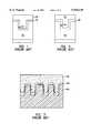
- titanium and aluminumreact, consuming a portion of the aluminum line up to three times the thickness of the original titanium underlayer. For example, if 500 ⁇ of titanium 20 is deposited under 5000 ⁇ of aluminum 22 (FIG. 1) in a recess 24 in a dielectric 26, and is fully reacted to form TiAl 3 , a structure will result that is 2000 ⁇ thick TiAl 3 28 under 3500 ⁇ aluminum 30. (See FIG. 2).
- TiAl 3 28While it is generally accepted that the presence of titanium is needed for via hole or trench filling, the formation of TiAl 3 28 causes some problems (see FIG. 3).
- the reaction to form TiAl 3 during the hot deposition or reflow processmay retard aluminum or alloy flow, and hence retard the filling process.
- Discontinuity of a sputtered, or PVD, titanium layer along a sidewall of a via or trenchresults in a poor physical barrier between the conductor and the interlayer dielectric oxide. Should the oxide outgas, the outgassing species may pass through the titanium layer when the wafer is heated for subsequent deposition steps. Hot aluminum or alloy is very sensitive to sputtering environment and surface conditions, and with any breach in the continuity of the titanium barrier/wetting layer, the outgassing species will negatively affect the fill of the aluminum or aluminum alloy.
- the present inventionprovides a barrier layer in the form of titanium nitride, titanium oxynitride, titanium carbonitride, or titanium silicide in a recess in a dielectric.
- a thin titanium layeris provided over the dielectric, and aluminum or aluminum alloy conductor is provided in the recess over the titanium layer.
- FIGS. 1-3are cross-sectional views showing prior art semiconductor devices.
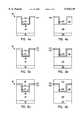
- FIGS. 4-8(including FIGS. 4(a)-4(b), 5(a)-5(b), 6(a)-(6b), 7(a)-7(b), and 8(a)-8(b) show cross-sections of semiconductor devices and methods of fabrication thereof in accordance with the present invention.
- FIGS. 4(a)-7(a)for an understanding of a first embodiment of the present inventive method and device.
- FIG. 4(a)shows a device 40 including a substrate 42 having a dielectric 44 in the form of an oxide formed thereover.
- the oxidehas a recess 46 in the form of a trench etched therein, having a bottom 48 and sidewalls 50.
- a thin barrier layer 52in the form of titanium nitride, titanium oxynitride, titanium carbonitride, or titanium silicide, is deposited using chemical vapor deposition (CVD).
- CVDchemical vapor deposition
- the titanium nitride source chemicali.e. tetrakis dimethyl amino titanium TDMAT, Ti N(CH 3 ) 2 ! 4 ! is a liquid heated to approximately 45° C.
- a carrier gassuch as helium
- a bubblerwhere it mixes with the TDMAT vapor.
- the gas mixtureis then introduced into a reaction chamber which is held at low pressure, typically in the range of 1 Torr.
- the TDMAT vaporwhen in contact with the heated surface of the semiconductor wafer, decomposes into a titanium nitride film, in the recess 46 along the sides 50 and bottom 48 of the trench 46.
- the wafer surfaceis typically heated to between 300 to 500° C.
- the resulting filmexhibits excellent coverage on the sides 50 and bottom 48 of the trench 46 that has been etched into the dielectric material 44.
- the system used for the metal depositionis a commercially available Applied Materials Endura 5500 sputtering system with multiple processing chambers.
- the chambersare connected and maintained under a base vacuum level ( ⁇ 1E-6 Torr).
- the waferis transferred from one chamber to another using a robot.
- the process for fillingrequires degas of the wafer at moderate temperatures on the Endura system, typically between 100 and 400° C. This is a standard process step for any metal deposition.
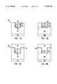
- the CVD titanium nitride layer 52is deposited in one chamber as described above, then the wafer is transferred to a chamber for titanium 54 deposition (FIG. 5(a)) in the trench 46, and then the wafer is moved to a chamber for aluminum or alloy 56 deposition (FIG.
- the capping PVD titanium 54which serves as an additional seed layer, could be deposited in a collimated chamber to ensure good step coverage. Any collimator aspect ratio could be used. Other techniques may also provide good step coverage. Examples include long throw sputtering and chemical vapor deposition. Titanium deposition conditions vary dramatically and the temperature can be from room temperature to 500° C. However, if the titanium deposition temperature is greater than a 100° C., the wafer should be cooled to less than a 100° C. prior to aluminum or aluminum alloy 56 deposition.
- the Alwas deposited using a three step deposition.
- the framework of the process for the Al depositionwas suggested by Applied Materials.
- the initial layer (2000-4000 ⁇ ) of Alis deposited at high power (9000-15000W) and at room temperature to ensure conformal coverage by the Al of the trench. This serves as a seed layer for subsequent Al deposition.
- the waferis then heated and the Al is deposited at low powers (1000-3000W, 3000-5000 ⁇ thick) such that the Al flows evenly into the trench. For increased throughput, the power is again increased (9000-15000W) in the final step to bring the total thickness to a predetermined value.
- the waferis cooled and returned to a wafer cassette.
- the aluminum or aluminum alloy 56is then polished to result in the structure shown in FIG. 7(a).
- the CVD titanium nitride 52could with advantage be any CVD layer that has characteristics as follows: conformal coverage of the trench 46; good barrier characteristics that prevent outgassing of the dielectric 44 (in this case, oxide) from adversely affecting the conductor, and smooth and uniform deposition across the wafer.
- the titanium nitride 52serves as a wetting layer for the deposition and flowing of aluminum or aluminum alloy on dielectrics.
- FIG. 8(a)is similar to FIG. 6(a) but shows aluminum or aluminum alloy 56 deposited directly on the barrier layer 52 with the barrier layer 52 and dielectric 44 at 425° C. or greater. Further process steps are then undertaken as described in regard to FIG.
- trenchescan be properly filled using a very thin or no titanium layer 54.
- Thisprovides several distinct advantages: 1) thinner or no titanium results in less or no TiAl 3 formation and improves the current carrying cross-section of the conductor; 2) less or no TiAl 3 results in a structure that is easier to chemically-mechanically polish; and 3) with less or no TiAl 3 , there will be little or no spiking of the grain boundaries, and with little or no spiking, there will not be current crowding effects.
- FIGS. 4(b)-7(b)show a process flow like that in FIGS. 4(a)-7(a), but instead of a trench being defined by the dielectric 100, a via hole 102 is defined thereby to adjacent a lower level metal layer 104 on a substrate 106.
- the process flowis the same as that shown in FIGS. 4(a)-7(a); however, the bottom of the trench no longer exists but is replaced by the top surface of the lower level metal layer 104, and the hole 102 has, for example, a circular cross-section.
- a barrier layer 108 of titanium nitride, titanium oxynitride, titanium carbonitride, or titanium silicideis deposited in the recess 102 defined by the dielectric 100.
- the process flowcontinues through deposition of a thin titanium layer 110 (FIG. 5(b)), and then an aluminum or aluminum alloy layer 112 (FIG. 6(b)) which is later polished to result in the structure shown in FIG. 7d.
- barrier layer 108is in the recess 102
- titanium layer 110is in the recess 102 over the barrier layer 108
- aluminum or aluminum alloy layer 112in the recess over the titanium layer 110.
- FIG. 8(b)is a view similar to FIG. 6(b) but again, a via hole 102 is defined by the dielectric 100 to a lower metal layer 104 on a substrate 106.
- additional stepsmay or may not be included to ensure good electrical conductivity. These may include incorporation of a surface treatment and additional metallic layers (i.e., Ti) underneath the TIN barrier layer.
Landscapes
- Engineering & Computer Science (AREA)
- Physics & Mathematics (AREA)
- Condensed Matter Physics & Semiconductors (AREA)
- General Physics & Mathematics (AREA)
- Computer Hardware Design (AREA)
- Microelectronics & Electronic Packaging (AREA)
- Power Engineering (AREA)
- Manufacturing & Machinery (AREA)
- Internal Circuitry In Semiconductor Integrated Circuit Devices (AREA)
Abstract
Description
This case is related to U.S. patent application Ser. No. 08/347,781, filed Nov. 30, 1994, now abandoned entitled PROCESS FOR IN-SITU DEPOSITION OF A Ti/TiN BARRIER METAL STACK, invented by Besser et al., U.S. patent application Ser. No. 08/393,625, filed Feb. 24, 1995, now U.S. Pat. No. 5,738,917 entitled PROCESS FOR IN-SITU DEPOSITION OF A Ti/TiN/Ti ALUMINUM UNDERLAYER, invented by Besser et al.
This invention relates to semiconductor devices, and more particularly, to the deposition of a conductor in a via or trench.
As semiconductor device geometries approach 0.25 μm feature size, increased attention has been directed to the difficulty in depositing aluminum or aluminum alloy into small vias holes or trenches. The use of multiple levels of interconnect metallization on a semiconductor device and shrinking feature size means that surface planarity, i.e., the flatness of the wafer surface, becomes increasingly important at critical operations in the processing of the device.
To improve surface planarity, various process steps and/or combinations of materials have been used. Years ago, it was standard practice on a multilevel metal structure to use sputtered aluminum or aluminum alloy in a trench or to form a via, i.e. an electrical connection between two levels of metal. This was done with the wafer surface between room temperature and 400° C.
The step coverage of the conductor deposited in this manner was found to be poor, leading to reliability problems due to the thinning of the conductor on the sides and bottom of the trench, or the sides of the via hole. This problem became progressively worse as additional layers were put down over an already non-planar surface.
An approach to solving this problem has been to use a separate material, such as tungsten, to form a via or plug. The excess tungsten on the surface of the wafer and not in the via hole or trench is etched or polished away, leaving a planar surface on top of which the next level of metal is deposited.
Another problem facing the semiconductor industry as the dimensions of interconnect lines continue to shrink is the etching of the conductor to form the patterned lines. The standard method in the integrated circuit industry involves depositing a blanket metal film, lithographically patterning the film, reactively ion etching to form lines, and encapsulating the lines with an oxide. Pitted sidewalls and residual polymer present reliability and contamination problems after the metal etch. These could be alleviated by a damascene approach to forming lines. The damascene approach differs from standard methods since the oxide is deposited, lithographically patterned, and etched to form trenches. Then the metal interconnect is deposited into these trenches. Excess metal is polished using special chemical-mechanical polish methods to leave lines of interconnect encapsulated on three sides with oxide. Damascene processing eliminates the need for metal etch and is expected to become standard practice in future technologies.
A need exists to fill trenches and via holes with sputtered aluminum or aluminum alloy. This has been accomplished thus far by increasing the temperature of the wafer during deposition of the conductor to between 450 to 600° C. At these temperatures (near the aluminum and aluminum alloy melting point), the conductor becomes softer, and can thus flow into small holes, completely filling them.
The mechanisms that lead to aluminum and aluminum alloy filling are not well understood. There are two general types of high-temperature processing: 1) reflow, and 2) hot Al. They are similar in that they both rely on temperatures between 400 to 600° C. The so-called reflow process is typically done by depositing the aluminum or aluminum alloy at a temperature between room temperature and 400° C. Afterward, the wafer is heated to between 500 to 600° C. The wafer is typically held at this temperature for several minutes, allowing the conductor to flow into the trench or via hole. The hot Al process is carried out in several steps. In the first step, a portion of the desired thickness of aluminum or aluminum alloy is deposited at relatively cold temperature (less than 400° C.), and then the wafer is heated up to between 500° C. to 600° C., and the remaining aluminum or aluminum alloy is deposited hot.
In either case, it is generally accepted that it is necessary to use a titanium wetting agent directly under the hot or reflowed conductor. It is very important that this titanium layer not be exposed to air before the conductor is deposited, as it will oxidize. In the absence of such titanium, the conductor will not flow or properly deposit in the bottom or on the sides of the trench or hole, leading to a void in the conductor.
At temperatures above 350° C., titanium and aluminum react, consuming a portion of the aluminum line up to three times the thickness of the original titanium underlayer. For example, if 500Å of titanium 20 is deposited under 5000Å of aluminum 22 (FIG. 1) in arecess 24 in a dielectric 26, and is fully reacted to form TiAl3, a structure will result that is 2000Åthick TiAl 3 28 under3500Å aluminum 30. (See FIG. 2).
While it is generally accepted that the presence of titanium is needed for via hole or trench filling, the formation ofTiAl 3 28 causes some problems (see FIG. 3). First, the formation of TiAl3, which has a lower electrical conductivity than aluminum oraluminum alloy 30, reduces the amount of current-carrying cross-section that is composed of the low resistivity aluminum and increases the electrical resistance of the metal interconnect lines. Second, TiAl3 is difficult to chemically-mechanically polish: so it is desired to have this TiAl3 layer as thin as possible or eliminate it altogether. Third, the reaction to form TiAl3 during the hot deposition or reflow process may retard aluminum or alloy flow, and hence retard the filling process. This retardation arises from the TiAl3 "spiking" through the grain boundaries in the aluminum or alloy by preferentially growing into the aluminum grains at the grain boundaries. Thermodynamically speaking, the formation of TiAl3 at the grain boundaries requires less surface energy than growth of TiAl3 into the bulk of the aluminum or alloy grain. The kinetics of TiAl3 formation, however, provide a loophole or process window in which titanium can be used to provide the necessary wetting property. By depositing the aluminum or aluminum alloy cold initially, the rate of TiAl3 formation is reduced, and an adequate, smooth seed layer of conductor is provided for subsequent deposition. Control of the titanium under layer thickness becomes critical. Too little, and there will not be enough of a wetting layer to enable the hole or trench filling. Too much, and the reaction forming TiAl3 will impede the hole or trench filling. Normal variations in hole or trench size, depth and shape, titanium deposition rate and uniformity make precise control of the titanium thickness in and around the via hole or trench difficult, leading to yield and reliability problems.
Discontinuity of a sputtered, or PVD, titanium layer along a sidewall of a via or trench results in a poor physical barrier between the conductor and the interlayer dielectric oxide. Should the oxide outgas, the outgassing species may pass through the titanium layer when the wafer is heated for subsequent deposition steps. Hot aluminum or alloy is very sensitive to sputtering environment and surface conditions, and with any breach in the continuity of the titanium barrier/wetting layer, the outgassing species will negatively affect the fill of the aluminum or aluminum alloy.
The present invention provides a barrier layer in the form of titanium nitride, titanium oxynitride, titanium carbonitride, or titanium silicide in a recess in a dielectric. A thin titanium layer is provided over the dielectric, and aluminum or aluminum alloy conductor is provided in the recess over the titanium layer.
FIGS. 1-3 are cross-sectional views showing prior art semiconductor devices; and
FIGS. 4-8 (including FIGS. 4(a)-4(b), 5(a)-5(b), 6(a)-(6b), 7(a)-7(b), and 8(a)-8(b) show cross-sections of semiconductor devices and methods of fabrication thereof in accordance with the present invention.
Reference is made to FIGS. 4(a)-7(a) for an understanding of a first embodiment of the present inventive method and device.
FIG. 4(a) shows adevice 40 including asubstrate 42 having a dielectric 44 in the form of an oxide formed thereover. The oxide has arecess 46 in the form of a trench etched therein, having abottom 48 andsidewalls 50. Athin barrier layer 52, in the form of titanium nitride, titanium oxynitride, titanium carbonitride, or titanium silicide, is deposited using chemical vapor deposition (CVD). In the case of atitanium nitride layer 52, the titanium nitride source chemical, i.e. tetrakis dimethyl amino titanium TDMAT, Ti N(CH3)2 !4 ! is a liquid heated to approximately 45° C. A carrier gas, such as helium, is passed through a bubbler, where it mixes with the TDMAT vapor. The gas mixture is then introduced into a reaction chamber which is held at low pressure, typically in the range of 1 Torr. The TDMAT vapor, when in contact with the heated surface of the semiconductor wafer, decomposes into a titanium nitride film, in therecess 46 along thesides 50 and bottom 48 of thetrench 46. The wafer surface is typically heated to between 300 to 500° C. The resulting film exhibits excellent coverage on thesides 50 and bottom 48 of thetrench 46 that has been etched into thedielectric material 44.
The system used for the metal deposition is a commercially available Applied Materials Endura 5500 sputtering system with multiple processing chambers. The chambers are connected and maintained under a base vacuum level (<1E-6 Torr). The wafer is transferred from one chamber to another using a robot. The process for filling requires degas of the wafer at moderate temperatures on the Endura system, typically between 100 and 400° C. This is a standard process step for any metal deposition. After degassing, the CVDtitanium nitride layer 52 is deposited in one chamber as described above, then the wafer is transferred to a chamber fortitanium 54 deposition (FIG. 5(a)) in thetrench 46, and then the wafer is moved to a chamber for aluminum oralloy 56 deposition (FIG. 6(a)) in thetrench 46. The cappingPVD titanium 54, which serves as an additional seed layer, could be deposited in a collimated chamber to ensure good step coverage. Any collimator aspect ratio could be used. Other techniques may also provide good step coverage. Examples include long throw sputtering and chemical vapor deposition. Titanium deposition conditions vary dramatically and the temperature can be from room temperature to 500° C. However, if the titanium deposition temperature is greater than a 100° C., the wafer should be cooled to less than a 100° C. prior to aluminum oraluminum alloy 56 deposition.
The Al was deposited using a three step deposition. The framework of the process for the Al deposition was suggested by Applied Materials. The initial layer (2000-4000 Å) of Al is deposited at high power (9000-15000W) and at room temperature to ensure conformal coverage by the Al of the trench. This serves as a seed layer for subsequent Al deposition. The wafer is then heated and the Al is deposited at low powers (1000-3000W, 3000-5000Å thick) such that the Al flows evenly into the trench. For increased throughput, the power is again increased (9000-15000W) in the final step to bring the total thickness to a predetermined value.
Following aluminum or aluminum alloy deposition into the trench or via, the wafer is cooled and returned to a wafer cassette. The aluminum oraluminum alloy 56 is then polished to result in the structure shown in FIG. 7(a).
TheCVD titanium nitride 52 could with advantage be any CVD layer that has characteristics as follows: conformal coverage of thetrench 46; good barrier characteristics that prevent outgassing of the dielectric 44 (in this case, oxide) from adversely affecting the conductor, and smooth and uniform deposition across the wafer. In effect, thetitanium nitride 52 serves as a wetting layer for the deposition and flowing of aluminum or aluminum alloy on dielectrics.
Several programs have been undertaken to establish the validity of the current process and device. When a CVD titaniumnitride barrier layer 52 was used in conjunction with atitanium layer 54 of less than 200 Å thick, fill was complete. This also occurred with thetitanium layer 54 less than 100 Å thick and also less than 50 Å thick. With a wafer temperature of 425° C. or greater, fill was complete with notitanium layer 54, and with a wafer temperature of 350° C., fill was substantially complete. (FIG. 8(a) is similar to FIG. 6(a) but shows aluminum oraluminum alloy 56 deposited directly on thebarrier layer 52 with thebarrier layer 52 and dielectric 44 at 425° C. or greater. Further process steps are then undertaken as described in regard to FIG. 7(a).) Thus, it has been demonstrated that trenches can be properly filled using a very thin or notitanium layer 54. This provides several distinct advantages: 1) thinner or no titanium results in less or no TiAl3 formation and improves the current carrying cross-section of the conductor; 2) less or no TiAl3 results in a structure that is easier to chemically-mechanically polish; and 3) with less or no TiAl3, there will be little or no spiking of the grain boundaries, and with little or no spiking, there will not be current crowding effects.
FIGS. 4(b)-7(b) show a process flow like that in FIGS. 4(a)-7(a), but instead of a trench being defined by the dielectric 100, a viahole 102 is defined thereby to adjacent a lowerlevel metal layer 104 on asubstrate 106. The process flow is the same as that shown in FIGS. 4(a)-7(a); however, the bottom of the trench no longer exists but is replaced by the top surface of the lowerlevel metal layer 104, and thehole 102 has, for example, a circular cross-section.
Similar to the previous described process and device, abarrier layer 108 of titanium nitride, titanium oxynitride, titanium carbonitride, or titanium silicide is deposited in therecess 102 defined by the dielectric 100. The process flow continues through deposition of a thin titanium layer 110 (FIG. 5(b)), and then an aluminum or aluminum alloy layer 112 (FIG. 6(b)) which is later polished to result in the structure shown in FIG. 7d.
Thus a portion of thebarrier layer 108 is in therecess 102, a portion oftitanium layer 110 is in therecess 102 over thebarrier layer 108, and a portion of the aluminum oraluminum alloy layer 112 in the recess over thetitanium layer 110.
FIG. 8(b) is a view similar to FIG. 6(b) but again, a viahole 102 is defined by the dielectric 100 to alower metal layer 104 on asubstrate 106.
It will be seen that the entire process flow is the same as that as described above in relation to a trench defined by the dielectric layer, and thus all of the discussion above, along with the advantages achieved, are attendant hereto.
For multilevel metal structures additional steps may or may not be included to ensure good electrical conductivity. These may include incorporation of a surface treatment and additional metallic layers (i.e., Ti) underneath the TIN barrier layer.
Claims (18)
1. A method of fabricating a semiconductor structure on a wafer, the method comprising:
providing an oxide dielectric on the wafer, said dielectric having a recess therein;
heating a surface of said wafer;
depositing a barrier layer of titanium nitride in said recess by a chemical vapor deposition process in which a titanium nitride source material is decomposed into titanium nitride by said heated surface of said wafer;
depositing a titanium layer in said recess over said barrier layer, said titanium layer deposited by a physical vapor deposition process to a thickness of less than 200 Å;
depositing an aluminum seed layer at room temperature in said recess over said titanium layer, wherein said seed layer is between 2000 and 4000Å thick;
heating said wafer to 425° C. or less; and
depositing a second aluminum layer over said seed layer.
2. The method of claim 1 and further providing the barrier layer comprises carbon.
3. The method of claim 1 and further providing that the titanium layer is less than 100Å thick.
4. The method of claim 1 and further providing that the titanium layer is less then 50Å thick.
5. A method of fabricating a semiconductor structure on a semiconductor wafer, the method comprising:
providing a dielectric having a recess therein;
heating a surface of said semiconductor wafer;
depositing a barrier layer including titanium and nitrogen in said recess using a chemical vapor deposition process in which a source material is decomposed into a titanium and nitrogen containing material by said heated surface of said semiconductor wafer;
holding said dielectric and barrier layer at a temperature of 425° C. or greater; and
providing a conductor in said recess over said barrier layer.
6. The method of claim 5 and further providing the barrier layer is titanium nitride.
7. The method of claim 5 and further providing the barrier layer comprises carbon.
8. A method of fabricating a semiconductor structure on a semiconductor wafer, the method comprising:
providing a dielectric having a recess therein;
heating a surface of said semiconductor wafer;
depositing a barrier layer including titanium and nitrogen in said recess using a chemical vapor deposition process in which a source material is decomposed into a titanium and nitrogen containing material by said heated surface of said semiconductor wafer;
holding said dielectric and barrier layer at a temperature of 350° C. or greater; and
providing a conductor in said recess over said barrier layer.
9. A method of fabricating a semiconductor structure on a wafer, the method comprising:
providing an oxide dielectric having a recess therein;
heating a surface of said wafer;
depositing a barrier layer of titanium nitride in said recess by a chemical vapor deposition process in which a titanium nitride source material is decomposed into titanium nitride by said heated surface of said wafer; and depositing an aluminum layer in said recess over said barrier layer.
10. The method of claim 9, wherein said aluminum layer comprises a seed layer and a second aluminum layer over said seed layer.
11. The method of claim 10, wherein said seed layer is between 2000 and 4000 Å thick.
12. The method of claim 10, wherein said seed layer is deposited at a temperature of less than approximately 100° C.
13. The method of claim 10, wherein said wafer is maintained at less than 425° C. while depositing said second aluminum layer.
14. The method of claim 13, wherein said wafer is maintained at approximately 350° C. while depositing said second aluminum layer.
15. The method of claim 9, further comprising depositing a titanium layer in said recess over said barrier layer.
16. The method of claim 15, further comprising cooling said wafer to below 100° C. prior to depositing said aluminum layer.
17. The method of claim 9, wherein said chemical vapor deposition comprises passing a carrier gas through tetrakis dimethyl amino titanium liquid.
18. The method of claim 1, wherein said chemical vapor deposition comprises passing a carrier gas through tetrakis dimethyl amino titanium liquid.
Priority Applications (2)
| Application Number | Priority Date | Filing Date | Title |
|---|---|---|---|
| US08/602,415US5918149A (en) | 1996-02-16 | 1996-02-16 | Deposition of a conductor in a via hole or trench |
| PCT/US1996/016707WO1997030479A1 (en) | 1996-02-16 | 1996-10-17 | Deposition of a conductor in a via hole or trench |
Applications Claiming Priority (1)
| Application Number | Priority Date | Filing Date | Title |
|---|---|---|---|
| US08/602,415US5918149A (en) | 1996-02-16 | 1996-02-16 | Deposition of a conductor in a via hole or trench |
Publications (1)
| Publication Number | Publication Date |
|---|---|
| US5918149Atrue US5918149A (en) | 1999-06-29 |
Family
ID=24411258
Family Applications (1)
| Application Number | Title | Priority Date | Filing Date |
|---|---|---|---|
| US08/602,415Expired - LifetimeUS5918149A (en) | 1996-02-16 | 1996-02-16 | Deposition of a conductor in a via hole or trench |
Country Status (2)
| Country | Link |
|---|---|
| US (1) | US5918149A (en) |
| WO (1) | WO1997030479A1 (en) |
Cited By (58)
| Publication number | Priority date | Publication date | Assignee | Title |
|---|---|---|---|---|
| US6069066A (en)* | 1998-12-09 | 2000-05-30 | United Microelectronics Corp. | Method of forming bonding pad |
| US6107176A (en)* | 1996-05-17 | 2000-08-22 | Micron Technology, Inc. | Method of fabricating a gate having a barrier of titanium silicide |
| US6144097A (en)* | 1998-05-13 | 2000-11-07 | Seiko Epson Corporation | Semiconductor device and method of fabricating the same |
| US6146991A (en)* | 1999-09-03 | 2000-11-14 | Taiwan Semiconductor Manufacturing Company | Barrier metal composite layer featuring a thin plasma vapor deposited titanium nitride capping layer |
| US6189209B1 (en)* | 1998-10-27 | 2001-02-20 | Texas Instruments Incorporated | Method for reducing via resistance in small high aspect ratio holes filled using aluminum extrusion |
| US6211072B1 (en)* | 1999-05-19 | 2001-04-03 | Advanced Micro Devices, Inc. | CVD Tin Barrier process with improved contact resistance |
| US6258466B1 (en)* | 1996-02-05 | 2001-07-10 | Micron Technology, Inc. | Metallization on titanium aluminide |
| US6277737B1 (en)* | 1998-09-02 | 2001-08-21 | Micron Technology, Inc. | Semiconductor processing methods and integrated circuitry |
| US20010023988A1 (en)* | 2000-03-27 | 2001-09-27 | Kabushiki Kaisha Toshiba | Semiconductor device |
| US20010033028A1 (en)* | 2000-03-27 | 2001-10-25 | Kazumi Matsumoto | Semiconductor devices and methods for manufacturing the same |
| US6326287B1 (en) | 1998-09-03 | 2001-12-04 | Seiko Epson Corporation | Semiconductor device and method of fabricating the same |
| US6334249B2 (en)* | 1997-04-22 | 2002-01-01 | Texas Instruments Incorporated | Cavity-filling method for reducing surface topography and roughness |
| US6358830B1 (en) | 1998-12-22 | 2002-03-19 | Seiko Epson Corporation | Method for manufacturing semiconductor device having interlayer dielectric film layers with like etch speeds |
| US6361880B1 (en) | 1999-12-22 | 2002-03-26 | International Business Machines Corporation | CVD/PVD/CVD/PVD fill process |
| WO2001099182A3 (en)* | 2000-06-21 | 2002-04-18 | Infineon Technologies Corp | Insitu diffusion barrier and copper metallization for improving reliability of semiconductor devices |
| US6387806B1 (en)* | 2000-09-06 | 2002-05-14 | Advanced Micro Devices, Inc. | Filling an interconnect opening with different types of alloys to enhance interconnect reliability |
| US6399490B1 (en) | 2000-06-29 | 2002-06-04 | International Business Machines Corporation | Highly conformal titanium nitride deposition process for high aspect ratio structures |
| US6429493B1 (en) | 1998-10-20 | 2002-08-06 | Seiko Epson Corporation | Semiconductor device and method for manufacturing semiconductor device |
| US6458703B2 (en) | 1998-09-04 | 2002-10-01 | Seiko Epson Corporation | Method for manufacturing semiconductor devices with allevration of thermal stress generation in conductive coating |
| US6468908B1 (en) | 2001-07-09 | 2002-10-22 | Taiwan Semiconductor Manufacturing Company | Al-Cu alloy sputtering method with post-metal quench |
| US6486555B2 (en)* | 1997-08-29 | 2002-11-26 | Seiko Epson Corporation | Semiconductor device having a contact structure using aluminum |
| US6509262B1 (en)* | 2000-11-30 | 2003-01-21 | Advanced Micro Devices, Inc. | Method of reducing electromigration in copper lines by calcium-doping copper surfaces in a chemical solution |
| US6570238B2 (en) | 1999-10-28 | 2003-05-27 | Agere Systems Inc. | Preweakened on chip metal fuse using dielectric trenches for barrier layer isolation |
| US20030211673A1 (en)* | 1997-12-18 | 2003-11-13 | Yoshitaka Nakamura | Dynamic random access memory with improved contact arrangements |
| US6660661B1 (en) | 2002-06-26 | 2003-12-09 | Cypress Semiconductor Corporation | Integrated circuit with improved RC delay |
| US20040041204A1 (en)* | 2002-08-29 | 2004-03-04 | Micron Technology, Inc. | Trench interconnect structure and formation method |
| US6723628B2 (en)* | 2000-03-27 | 2004-04-20 | Seiko Epson Corporation | Method for forming bonding pad structures in semiconductor devices |
| US20040121584A1 (en)* | 2002-12-16 | 2004-06-24 | Lee Ja Suk | Method of manufacturing a semiconductor device |
| US6756302B1 (en)* | 1997-11-13 | 2004-06-29 | Cypress Semiconductor Corporation | Low temperature metallization process |
| US20040137715A1 (en)* | 2002-12-30 | 2004-07-15 | Ki Min Lee | Methods of manufacturing semiconductor devices |
| US6764945B2 (en)* | 2001-01-23 | 2004-07-20 | Renesas Technology Corp. | Method of manufacturing a multilayer metallization structure with non-directional sputtering method |
| EP1458020A3 (en)* | 2003-03-11 | 2005-01-12 | Texas Instruments Incorporated | Method for forming a void free VIA |
| US20050074966A1 (en)* | 1999-09-02 | 2005-04-07 | Micron Technology, Inc. | Local multilayered metallization |
| US6904675B1 (en)* | 1996-09-27 | 2005-06-14 | Hewlett-Packard Development, L.P. | Method of forming electrical interconnects having electromigration-inhibiting plugs |
| US6977217B1 (en) | 2002-12-03 | 2005-12-20 | Cypress Semiconductor Corporation | Aluminum-filled via structure with barrier layer |
| US7018942B1 (en) | 2002-06-26 | 2006-03-28 | Cypress Semiconductor Corporation | Integrated circuit with improved RC delay |
| US7026235B1 (en) | 2002-02-07 | 2006-04-11 | Cypress Semiconductor Corporation | Dual-damascene process and associated floating metal structures |
| US20060113674A1 (en)* | 2001-03-01 | 2006-06-01 | Kabushiki Kaisha Toshiba | Semiconductor device and manufacturing method of semiconductor device |
| US20060149638A1 (en)* | 2005-01-06 | 2006-07-06 | Allen Anita L | Electronic personalized clothing makeover assistant |
| US7192867B1 (en) | 2002-06-26 | 2007-03-20 | Cypress Semiconductor Corporation | Protection of low-k dielectric in a passivation level |
| US7227212B1 (en) | 2002-01-29 | 2007-06-05 | Cypress Semiconductor Corporation | Method of forming a floating metal structure in an integrated circuit |
| US7226858B2 (en) | 2004-09-30 | 2007-06-05 | Microchip Technology Incorporated | Submicron contact fill using a CVD TiN barrier and high temperature PVD aluminum alloy deposition |
| US20110269308A1 (en)* | 2010-04-30 | 2011-11-03 | Elpida Memory, Inc. | Method for manufacturing semiconductor device |
| US20130260555A1 (en)* | 2012-03-28 | 2013-10-03 | Bhushan N. ZOPE | Method of enabling seamless cobalt gap-fill |
| US20140361386A1 (en)* | 2011-05-17 | 2014-12-11 | United Microelectronics Corp. | Semiconductor device |
| US20150093891A1 (en)* | 2013-09-27 | 2015-04-02 | Applied Materials, Inc. | Method of enabling seamless cobalt gap-fill |
| US9093455B2 (en) | 2013-07-16 | 2015-07-28 | Taiwan Semiconductor Manufacturing Company Limited | Back-end-of-line (BEOL) interconnect structure |
| US11361978B2 (en) | 2018-07-25 | 2022-06-14 | Applied Materials, Inc. | Gas delivery module |
| US11462417B2 (en) | 2017-08-18 | 2022-10-04 | Applied Materials, Inc. | High pressure and high temperature anneal chamber |
| US11527421B2 (en) | 2017-11-11 | 2022-12-13 | Micromaterials, LLC | Gas delivery system for high pressure processing chamber |
| US11581183B2 (en) | 2018-05-08 | 2023-02-14 | Applied Materials, Inc. | Methods of forming amorphous carbon hard mask layers and hard mask layers formed therefrom |
| US11610773B2 (en) | 2017-11-17 | 2023-03-21 | Applied Materials, Inc. | Condenser system for high pressure processing system |
| US11694912B2 (en) | 2017-08-18 | 2023-07-04 | Applied Materials, Inc. | High pressure and high temperature anneal chamber |
| US11705337B2 (en) | 2017-05-25 | 2023-07-18 | Applied Materials, Inc. | Tungsten defluorination by high pressure treatment |
| US11749555B2 (en) | 2018-12-07 | 2023-09-05 | Applied Materials, Inc. | Semiconductor processing system |
| US11881411B2 (en) | 2018-03-09 | 2024-01-23 | Applied Materials, Inc. | High pressure annealing process for metal containing materials |
| US11901222B2 (en) | 2020-02-17 | 2024-02-13 | Applied Materials, Inc. | Multi-step process for flowable gap-fill film |
| US12198951B2 (en) | 2017-03-10 | 2025-01-14 | Applied Materials, Inc. | High pressure wafer processing systems and related methods |
Families Citing this family (1)
| Publication number | Priority date | Publication date | Assignee | Title |
|---|---|---|---|---|
| US6245653B1 (en) | 1998-04-30 | 2001-06-12 | Applied Materials, Inc. | Method of filling an opening in an insulating layer |
Citations (19)
| Publication number | Priority date | Publication date | Assignee | Title |
|---|---|---|---|---|
| US4673623A (en)* | 1985-05-06 | 1987-06-16 | The Board Of Trustees Of The Leland Stanford Junior University | Layered and homogeneous films of aluminum and aluminum/silicon with titanium and tungsten for multilevel interconnects |
| US4823182A (en)* | 1986-11-21 | 1989-04-18 | Kabushiki Kaisha Toshiba | Semiconductor device with a diffusion barrier contact of a refractory metal nitride and either carbon or boron |
| EP0387835A2 (en)* | 1989-03-14 | 1990-09-19 | Kabushiki Kaisha Toshiba | Semiconductor device and method of manufacturing the same |
| US5071714A (en)* | 1989-04-17 | 1991-12-10 | International Business Machines Corporation | Multilayered intermetallic connection for semiconductor devices |
| JPH04120727A (en)* | 1990-09-12 | 1992-04-21 | Sony Corp | Manufacture of semiconductor device |
| EP0525637A1 (en)* | 1991-07-24 | 1993-02-03 | Applied Materials, Inc. | Method for the formation of tin barrier layer with preferential (111) crystallographic orientation |
| EP0552968A2 (en)* | 1992-01-23 | 1993-07-28 | Samsung Electronics Co. Ltd. | Semiconductor device including a wiring layer |
| US5240880A (en)* | 1992-05-05 | 1993-08-31 | Zilog, Inc. | Ti/TiN/Ti contact metallization |
| US5246881A (en)* | 1993-04-14 | 1993-09-21 | Micron Semiconductor, Inc. | Low-pressure chemical vapor deposition process for depositing high-density, highly-conformal, titanium nitride films of low bulk resistivity |
| US5290731A (en)* | 1991-03-07 | 1994-03-01 | Sony Corporation | Aluminum metallization method |
| EP0598422A1 (en)* | 1992-10-15 | 1994-05-25 | Koninklijke Philips Electronics N.V. | Method of forming a Ti and a TiN layer on a semiconductor body by a sputtering process, comprising an additional step of cleaning the target |
| US5360995A (en)* | 1993-09-14 | 1994-11-01 | Texas Instruments Incorporated | Buffered capped interconnect for a semiconductor device |
| US5371042A (en)* | 1992-06-16 | 1994-12-06 | Applied Materials, Inc. | Method of filling contacts in semiconductor devices |
| US5380678A (en)* | 1991-03-12 | 1995-01-10 | Yu; Chang | Bilayer barrier metal method for obtaining 100% step-coverage in contact vias without junction degradation |
| US5385867A (en)* | 1993-03-26 | 1995-01-31 | Matsushita Electric Industrial Co., Ltd. | Method for forming a multi-layer metallic wiring structure |
| US5418388A (en)* | 1993-06-18 | 1995-05-23 | Mitsubishi Denki Kabushiki Kaisha | Semiconductor device having a capacitor with an adhesion layer |
| EP0716447A2 (en)* | 1994-12-05 | 1996-06-12 | AT&T Corp. | Metal layers formed as a composite of sub-layers and devices including same |
| US5543357A (en)* | 1993-12-08 | 1996-08-06 | Nec Corporation | Process of manufacturing a semiconductor device by filling a via hole in an interlayered film of the device with wiring metal |
| US5627102A (en)* | 1993-03-23 | 1997-05-06 | Kawasaki Steel Corporation | Method for making metal interconnection with chlorine plasma etch |
- 1996
- 1996-02-16USUS08/602,415patent/US5918149A/ennot_activeExpired - Lifetime
- 1996-10-17WOPCT/US1996/016707patent/WO1997030479A1/enactiveApplication Filing
Patent Citations (20)
| Publication number | Priority date | Publication date | Assignee | Title |
|---|---|---|---|---|
| US4673623A (en)* | 1985-05-06 | 1987-06-16 | The Board Of Trustees Of The Leland Stanford Junior University | Layered and homogeneous films of aluminum and aluminum/silicon with titanium and tungsten for multilevel interconnects |
| US4823182A (en)* | 1986-11-21 | 1989-04-18 | Kabushiki Kaisha Toshiba | Semiconductor device with a diffusion barrier contact of a refractory metal nitride and either carbon or boron |
| EP0387835A2 (en)* | 1989-03-14 | 1990-09-19 | Kabushiki Kaisha Toshiba | Semiconductor device and method of manufacturing the same |
| US5071714A (en)* | 1989-04-17 | 1991-12-10 | International Business Machines Corporation | Multilayered intermetallic connection for semiconductor devices |
| JPH04120727A (en)* | 1990-09-12 | 1992-04-21 | Sony Corp | Manufacture of semiconductor device |
| US5290731A (en)* | 1991-03-07 | 1994-03-01 | Sony Corporation | Aluminum metallization method |
| US5380678A (en)* | 1991-03-12 | 1995-01-10 | Yu; Chang | Bilayer barrier metal method for obtaining 100% step-coverage in contact vias without junction degradation |
| EP0525637A1 (en)* | 1991-07-24 | 1993-02-03 | Applied Materials, Inc. | Method for the formation of tin barrier layer with preferential (111) crystallographic orientation |
| EP0552968A2 (en)* | 1992-01-23 | 1993-07-28 | Samsung Electronics Co. Ltd. | Semiconductor device including a wiring layer |
| US5240880A (en)* | 1992-05-05 | 1993-08-31 | Zilog, Inc. | Ti/TiN/Ti contact metallization |
| US5317187A (en)* | 1992-05-05 | 1994-05-31 | Zilog, Inc. | Ti/TiN/Ti contact metallization |
| US5371042A (en)* | 1992-06-16 | 1994-12-06 | Applied Materials, Inc. | Method of filling contacts in semiconductor devices |
| EP0598422A1 (en)* | 1992-10-15 | 1994-05-25 | Koninklijke Philips Electronics N.V. | Method of forming a Ti and a TiN layer on a semiconductor body by a sputtering process, comprising an additional step of cleaning the target |
| US5627102A (en)* | 1993-03-23 | 1997-05-06 | Kawasaki Steel Corporation | Method for making metal interconnection with chlorine plasma etch |
| US5385867A (en)* | 1993-03-26 | 1995-01-31 | Matsushita Electric Industrial Co., Ltd. | Method for forming a multi-layer metallic wiring structure |
| US5246881A (en)* | 1993-04-14 | 1993-09-21 | Micron Semiconductor, Inc. | Low-pressure chemical vapor deposition process for depositing high-density, highly-conformal, titanium nitride films of low bulk resistivity |
| US5418388A (en)* | 1993-06-18 | 1995-05-23 | Mitsubishi Denki Kabushiki Kaisha | Semiconductor device having a capacitor with an adhesion layer |
| US5360995A (en)* | 1993-09-14 | 1994-11-01 | Texas Instruments Incorporated | Buffered capped interconnect for a semiconductor device |
| US5543357A (en)* | 1993-12-08 | 1996-08-06 | Nec Corporation | Process of manufacturing a semiconductor device by filling a via hole in an interlayered film of the device with wiring metal |
| EP0716447A2 (en)* | 1994-12-05 | 1996-06-12 | AT&T Corp. | Metal layers formed as a composite of sub-layers and devices including same |
Non-Patent Citations (44)
| Title |
|---|
| Brouillard, et al., "Thin Film Metallurgy With Sandwich Barrier Layer", IBM Technical Disclosure Bulletin, vol. 21, No. 2, Jul. 1978, p. 576. |
| Brouillard, et al., Thin Film Metallurgy With Sandwich Barrier Layer , IBM Technical Disclosure Bulletin, vol. 21, No. 2, Jul. 1978, p. 576.* |
| Eizenberg et al., "Chemical Vapor Deposited TiCN: A New Barrier Metallization For Submicron Via and Contact Applications", J. Vac. Sci. Technol. A 13 (3) , May/Jun. 1995, pp. 590-595. |
| Eizenberg et al., Chemical Vapor Deposited TiCN: A New Barrier Metallization For Submicron Via and Contact Applications , J. Vac. Sci. Technol. A 13 (3) , May/Jun. 1995, pp. 590 595.* |
| Estabil et al., "Electromigration Improvements with Titanium Underlay and Overlay in A1 (Cu) Metallurgy", VMIC Conference, TH-0359-0/91/0000-0242, Jun. 11-12, 1991, pp. 242-248. |
| Estabil et al., Electromigration Improvements with Titanium Underlay and Overlay in A1 (Cu) Metallurgy , VMIC Conference, TH 0359 0/91/0000 0242, Jun. 11 12, 1991, pp. 242 248.* |
| Gardner et al., "Homogeneous and Layered Films of Aluminum/Silicon With Titanium for Multilevel Interconnects", V-MIC Conf., Jun . 25-26, 1985, pp. 102-113. |
| Gardner et al., Homogeneous and Layered Films of Aluminum/Silicon With Titanium for Multilevel Interconnects , V MIC Conf., Jun . 25 26, 1985, pp. 102 113.* |
| Gniewek et al., "Titanium Overlay on Metallurgy", IBM Technical Disclosure Bulletin, vol. 13, No. 5, Oct. 1970, p. 1124. |
| Gniewek et al., Titanium Overlay on Metallurgy , IBM Technical Disclosure Bulletin, vol. 13, No. 5, Oct. 1970, p. 1124.* |
| Hewes et al., "Interaction of Titanium Cap and Aluminum Alloys With Tin Barrier Layer on Annealed Metal Sheet Resistance and on Electromigration", VMIC Conference, 1994 ISMIC--103/94/0278, Jun. 7-8, 1994, pp. 278-280. |
| Hewes et al., Interaction of Titanium Cap and Aluminum Alloys With Tin Barrier Layer on Annealed Metal Sheet Resistance and on Electromigration , VMIC Conference, 1994 ISMIC 103/94/0278, Jun. 7 8, 1994, pp. 278 280.* |
| Ho et al., "Sputtered Metallurgy Process For Electromigration Improvement of A1-Cu Interconnections", IBM Technical Disclosure Bulletin, vol. 21, No. 11, Apr. 1979, pp. 4527-4528. |
| Ho et al., Sputtered Metallurgy Process For Electromigration Improvement of A1 Cu Interconnections , IBM Technical Disclosure Bulletin, vol. 21, No. 11, Apr. 1979, pp. 4527 4528.* |
| Hoshino et al., "Hyper(111)-Textured A1 Interconnects By Reflowed A1 on the CVD-TiN/cvd-Ti Film", VMIC Conference, 1995 ISMIC-104/95/0589, Jun. 27-29, 1995, pp. 589-593. |
| Hoshino et al., Hyper(111) Textured A1 Interconnects By Reflowed A1 on the CVD TiN/cvd Ti Film , VMIC Conference, 1995 ISMIC 104/95/0589, Jun. 27 29, 1995, pp. 589 593.* |
| Howard et al., "Intermetallic Compounds of A1 and Transitions Metals: Effect of Electromigration In 1-2-υM-Wide Lines", J. Appl. Phys. 49(7), Jul. 1978, pp. 4083-4093. |
| Howard et al., Intermetallic Compounds of A1 and Transitions Metals: Effect of Electromigration In 1 2 M Wide Lines , J. Appl. Phys. 49(7), Jul. 1978, pp. 4083 4093.* |
| Hultman, et al., "Interfacial Reactions in Single-Crystal-TiN (100) /A1/ Polycrystalline-TiN Multilayer Thin Films", Thin Solid Films, vol. 215, No. 2, Aug. 14, 1992, pp. 152-161. |
| Hultman, et al., Interfacial Reactions in Single Crystal TiN (100) /A1/ Polycrystalline TiN Multilayer Thin Films , Thin Solid Films, vol. 215, No. 2, Aug. 14, 1992, pp. 152 161.* |
| Inoue et al., "Behavior of TiN and Ti Barrier Metals In A1-Barrier-A1 Via Hole Metallization", J. Electrochem. Soc., vol. 141, No. 4, Apr. 1994, pp. 1056-1061. |
| Inoue et al., "Effects of TiN/Ti Cap Layers on Improving Electromigration in A1 Based Multi-Layered Interconnects", VMIC Conference, 1994 ISMIC-103/94/0275, Jun. 7-8, 1994, pp. 275-277. |
| Inoue et al., Behavior of TiN and Ti Barrier Metals In A1 Barrier A1 Via Hole Metallization , J. Electrochem. Soc., vol. 141, No. 4, Apr. 1994, pp. 1056 1061.* |
| Inoue et al., Effects of TiN/Ti Cap Layers on Improving Electromigration in A1 Based Multi Layered Interconnects , VMIC Conference, 1994 ISMIC 103/94/0275, Jun. 7 8, 1994, pp. 275 277.* |
| Joshi, et al., "Collimated Sputtering of TiN/Ti Liners into Sub-Half-Micrometer High Aspect Ratio Contacts/Lines", Applied Physics Letters, vol. 61, No. 21, Nov. 23, 1992, pp. 2613-2615. |
| Joshi, et al., Collimated Sputtering of TiN/Ti Liners into Sub Half Micrometer High Aspect Ratio Contacts/Lines , Applied Physics Letters, vol. 61, No. 21, Nov. 23, 1992, pp. 2613 2615.* |
| Licata et al., "Dual Damascene Al Wiring For 256M Dram", VMIC Conference, 1995 ISMIC-104/95/0596, Jun. 27-29, 1995, pp. 596-602. |
| Licata et al., Dual Damascene Al Wiring For 256M Dram , VMIC Conference, 1995 ISMIC 104/95/0596, Jun. 27 29, 1995, pp. 596 602.* |
| Maheo, et al., "Microstructure and Electrical Resistivity of TiN Films Deposited on Heated and Negatively Biased Silicon Substrates", Thin Solid Films, vol. 237, No. 1/02, Jan. 1, 1994, pp. 78-86. |
| Maheo, et al., Microstructure and Electrical Resistivity of TiN Films Deposited on Heated and Negatively Biased Silicon Substrates , Thin Solid Films, vol. 237, No. 1/02, Jan. 1, 1994, pp. 78 86.* |
| Massiani, et al., "Effect of a Titanium Underlayer on the Corrosion Behaviour of Physically Vapour Deposited Titanium Nitride Films", Thin Solid Films, vol. 217, No. 1/02, Sep. 30, 1992, pp. 31-37. |
| Massiani, et al., Effect of a Titanium Underlayer on the Corrosion Behaviour of Physically Vapour Deposited Titanium Nitride Films , Thin Solid Films, vol. 217, No. 1/02, Sep. 30, 1992, pp. 31 37.* |
| Rodbell et al., "Texture Effects on the Electromigration Behavior of Layered Ti/AlCu/Ti Films", Mat. Res. Soc. Symp. Proc., vol. 265, 1992, pp. 107-113. |
| Rodbell et al., Texture Effects on the Electromigration Behavior of Layered Ti/AlCu/Ti Films , Mat. Res. Soc. Symp. Proc., vol. 265, 1992, pp. 107 113.* |
| Sandhu et al., "Metalorganic Chemical Vapor Deposition of TiN Films For Advanced Metallization", Appl. Phys. Lett 62(3), Jan. 18,1993, pp. 240-242. |
| Sandhu et al., Metalorganic Chemical Vapor Deposition of TiN Films For Advanced Metallization , Appl. Phys. Lett 62(3), Jan. 18,1993, pp. 240 242.* |
| Shen et al., "A Highly Reliable Aluminum Metallization for Micron and Submicron VLSI Applications", V-MIC Conf., CH 2337-4/86/0000-0191, Jun. 9-10, 1986, pp. 191-197. |
| Shen et al., A Highly Reliable Aluminum Metallization for Micron and Submicron VLSI Applications , V MIC Conf., CH 2337 4/86/0000 0191, Jun. 9 10, 1986, pp. 191 197.* |
| Shih, et al., "Ti/Ti-N Hf/Hf-N and W/W-N Multilayer Films with High Mechanical Hardness", Applied Physics Letters, vol. 61, No. 6, Aug. 10; 1992, pp. 654-656. |
| Shih, et al., Ti/Ti N Hf/Hf N and W/W N Multilayer Films with High Mechanical Hardness , Applied Physics Letters, vol. 61, No. 6, Aug. 10; 1992, pp. 654 656.* |
| Tracy et al., "Texture in Multilayer Metallization Structures", J. Appl. Phys. 76(5), Sep. 1, 1994, pp. 2671-2680. |
| Tracy et al., Texture in Multilayer Metallization Structures , J. Appl. Phys. 76(5), Sep. 1, 1994, pp. 2671 2680.* |
| Wendt, H. et al., "Process Integration for Barrier Layers and A1-Alloys using a Sputtering Cluster Tool", Microelectronic Engineering, vol. 19 pp. 371-374, 1992. |
| Wendt, H. et al., Process Integration for Barrier Layers and A1 Alloys using a Sputtering Cluster Tool , Microelectronic Engineering, vol. 19 pp. 371 374, 1992.* |
Cited By (92)
| Publication number | Priority date | Publication date | Assignee | Title |
|---|---|---|---|---|
| US6258466B1 (en)* | 1996-02-05 | 2001-07-10 | Micron Technology, Inc. | Metallization on titanium aluminide |
| US6107176A (en)* | 1996-05-17 | 2000-08-22 | Micron Technology, Inc. | Method of fabricating a gate having a barrier of titanium silicide |
| US6904675B1 (en)* | 1996-09-27 | 2005-06-14 | Hewlett-Packard Development, L.P. | Method of forming electrical interconnects having electromigration-inhibiting plugs |
| US6334249B2 (en)* | 1997-04-22 | 2002-01-01 | Texas Instruments Incorporated | Cavity-filling method for reducing surface topography and roughness |
| US6486555B2 (en)* | 1997-08-29 | 2002-11-26 | Seiko Epson Corporation | Semiconductor device having a contact structure using aluminum |
| US6756302B1 (en)* | 1997-11-13 | 2004-06-29 | Cypress Semiconductor Corporation | Low temperature metallization process |
| US20030211673A1 (en)* | 1997-12-18 | 2003-11-13 | Yoshitaka Nakamura | Dynamic random access memory with improved contact arrangements |
| US6144097A (en)* | 1998-05-13 | 2000-11-07 | Seiko Epson Corporation | Semiconductor device and method of fabricating the same |
| US6617246B2 (en)* | 1998-09-02 | 2003-09-09 | Micron Technology, Inc. | Semiconductor processing methods and integrated circuitry |
| US6570252B1 (en) | 1998-09-02 | 2003-05-27 | Micron Technology, Inc. | Integrated circuitry |
| US6277737B1 (en)* | 1998-09-02 | 2001-08-21 | Micron Technology, Inc. | Semiconductor processing methods and integrated circuitry |
| US6822328B2 (en) | 1998-09-02 | 2004-11-23 | Micron Technology, Inc. | Integrated circuitry |
| US20030008491A1 (en)* | 1998-09-02 | 2003-01-09 | Sandhu Gurtej S. | Integrated circuitry |
| US6326287B1 (en) | 1998-09-03 | 2001-12-04 | Seiko Epson Corporation | Semiconductor device and method of fabricating the same |
| US6458703B2 (en) | 1998-09-04 | 2002-10-01 | Seiko Epson Corporation | Method for manufacturing semiconductor devices with allevration of thermal stress generation in conductive coating |
| US6429493B1 (en) | 1998-10-20 | 2002-08-06 | Seiko Epson Corporation | Semiconductor device and method for manufacturing semiconductor device |
| US6511910B2 (en)* | 1998-10-20 | 2003-01-28 | Seiko Epson Corporation | Method for manufacturing semiconductor devices |
| US6189209B1 (en)* | 1998-10-27 | 2001-02-20 | Texas Instruments Incorporated | Method for reducing via resistance in small high aspect ratio holes filled using aluminum extrusion |
| US6443743B1 (en)* | 1998-10-27 | 2002-09-03 | Texas Instruments Incorporated | Method for reducing via resistance in small high aspect ratio holes filled using aluminum extrusion |
| US6069066A (en)* | 1998-12-09 | 2000-05-30 | United Microelectronics Corp. | Method of forming bonding pad |
| US6358830B1 (en) | 1998-12-22 | 2002-03-19 | Seiko Epson Corporation | Method for manufacturing semiconductor device having interlayer dielectric film layers with like etch speeds |
| US6211072B1 (en)* | 1999-05-19 | 2001-04-03 | Advanced Micro Devices, Inc. | CVD Tin Barrier process with improved contact resistance |
| US20050074966A1 (en)* | 1999-09-02 | 2005-04-07 | Micron Technology, Inc. | Local multilayered metallization |
| US7388289B1 (en) | 1999-09-02 | 2008-06-17 | Micron Technology, Inc. | Local multilayered metallization |
| US7375026B2 (en) | 1999-09-02 | 2008-05-20 | Micron Technology, Inc. | Local multilayered metallization |
| US20060199387A1 (en)* | 1999-09-02 | 2006-09-07 | Micron Technology, Inc. | Local multilayered metallization |
| US6146991A (en)* | 1999-09-03 | 2000-11-14 | Taiwan Semiconductor Manufacturing Company | Barrier metal composite layer featuring a thin plasma vapor deposited titanium nitride capping layer |
| US6570238B2 (en) | 1999-10-28 | 2003-05-27 | Agere Systems Inc. | Preweakened on chip metal fuse using dielectric trenches for barrier layer isolation |
| US6361880B1 (en) | 1999-12-22 | 2002-03-26 | International Business Machines Corporation | CVD/PVD/CVD/PVD fill process |
| US6812123B2 (en) | 2000-03-27 | 2004-11-02 | Seiko Epson Corporation | Semiconductor devices and methods for manufacturing the same |
| US6723628B2 (en)* | 2000-03-27 | 2004-04-20 | Seiko Epson Corporation | Method for forming bonding pad structures in semiconductor devices |
| US20010023988A1 (en)* | 2000-03-27 | 2001-09-27 | Kabushiki Kaisha Toshiba | Semiconductor device |
| US6909191B2 (en) | 2000-03-27 | 2005-06-21 | Kabushiki Kaisha Toshiba | Semiconductor device |
| US20010033028A1 (en)* | 2000-03-27 | 2001-10-25 | Kazumi Matsumoto | Semiconductor devices and methods for manufacturing the same |
| WO2001099182A3 (en)* | 2000-06-21 | 2002-04-18 | Infineon Technologies Corp | Insitu diffusion barrier and copper metallization for improving reliability of semiconductor devices |
| KR100788064B1 (en) | 2000-06-21 | 2007-12-21 | 인피니언 테크놀로지스 노쓰 아메리카 코포레이션 | How to Form Metallization for Semiconductor Devices |
| US6399490B1 (en) | 2000-06-29 | 2002-06-04 | International Business Machines Corporation | Highly conformal titanium nitride deposition process for high aspect ratio structures |
| US6387806B1 (en)* | 2000-09-06 | 2002-05-14 | Advanced Micro Devices, Inc. | Filling an interconnect opening with different types of alloys to enhance interconnect reliability |
| US6509262B1 (en)* | 2000-11-30 | 2003-01-21 | Advanced Micro Devices, Inc. | Method of reducing electromigration in copper lines by calcium-doping copper surfaces in a chemical solution |
| US6764945B2 (en)* | 2001-01-23 | 2004-07-20 | Renesas Technology Corp. | Method of manufacturing a multilayer metallization structure with non-directional sputtering method |
| US7088001B2 (en) | 2001-01-23 | 2006-08-08 | Hitachi, Ltd. | Semiconductor integrated circuit device with a metallization structure |
| US20060113674A1 (en)* | 2001-03-01 | 2006-06-01 | Kabushiki Kaisha Toshiba | Semiconductor device and manufacturing method of semiconductor device |
| US6468908B1 (en) | 2001-07-09 | 2002-10-22 | Taiwan Semiconductor Manufacturing Company | Al-Cu alloy sputtering method with post-metal quench |
| US7227212B1 (en) | 2002-01-29 | 2007-06-05 | Cypress Semiconductor Corporation | Method of forming a floating metal structure in an integrated circuit |
| US7026235B1 (en) | 2002-02-07 | 2006-04-11 | Cypress Semiconductor Corporation | Dual-damascene process and associated floating metal structures |
| US7018942B1 (en) | 2002-06-26 | 2006-03-28 | Cypress Semiconductor Corporation | Integrated circuit with improved RC delay |
| US6841878B1 (en) | 2002-06-26 | 2005-01-11 | Cypress Semiconductor Corporation | Integrated circuit with improved RC delay |
| US7192867B1 (en) | 2002-06-26 | 2007-03-20 | Cypress Semiconductor Corporation | Protection of low-k dielectric in a passivation level |
| US6660661B1 (en) | 2002-06-26 | 2003-12-09 | Cypress Semiconductor Corporation | Integrated circuit with improved RC delay |
| US7943503B2 (en) | 2002-08-29 | 2011-05-17 | Micron Technology, Inc. | Trench interconnect structure and formation method |
| US20110212618A1 (en)* | 2002-08-29 | 2011-09-01 | Ireland Philip J | Trench interconnect structure and formation method |
| US20040041204A1 (en)* | 2002-08-29 | 2004-03-04 | Micron Technology, Inc. | Trench interconnect structure and formation method |
| US7138719B2 (en) | 2002-08-29 | 2006-11-21 | Micron Technology, Inc. | Trench interconnect structure and formation method |
| US20060189135A1 (en)* | 2002-08-29 | 2006-08-24 | Micron Technology, Inc. | Trench interconnect structure and formation method |
| US6977217B1 (en) | 2002-12-03 | 2005-12-20 | Cypress Semiconductor Corporation | Aluminum-filled via structure with barrier layer |
| US20060003578A1 (en)* | 2002-12-16 | 2006-01-05 | Lee Jae S | Method of manufacturing a semiconductor device |
| US7074716B2 (en) | 2002-12-16 | 2006-07-11 | Dongbu Electronics Co., Ltd. | Method of manufacturing a semiconductor device |
| US6964920B2 (en) | 2002-12-16 | 2005-11-15 | Dongbu Electronics Co., Ltd. | Method of manufacturing a semiconductor device |
| US20040121584A1 (en)* | 2002-12-16 | 2004-06-24 | Lee Ja Suk | Method of manufacturing a semiconductor device |
| US20040137715A1 (en)* | 2002-12-30 | 2004-07-15 | Ki Min Lee | Methods of manufacturing semiconductor devices |
| US6977437B2 (en) | 2003-03-11 | 2005-12-20 | Texas Instruments Incorporated | Method for forming a void free via |
| US7323409B2 (en) | 2003-03-11 | 2008-01-29 | Texas Instruments Incorporated | Method for forming a void free via |
| US20050146035A1 (en)* | 2003-03-11 | 2005-07-07 | Griffin Alfred J.Jr. | Method for forming a void free via |
| EP1458020A3 (en)* | 2003-03-11 | 2005-01-12 | Texas Instruments Incorporated | Method for forming a void free VIA |
| US7226858B2 (en) | 2004-09-30 | 2007-06-05 | Microchip Technology Incorporated | Submicron contact fill using a CVD TiN barrier and high temperature PVD aluminum alloy deposition |
| US20060149638A1 (en)* | 2005-01-06 | 2006-07-06 | Allen Anita L | Electronic personalized clothing makeover assistant |
| US20110269308A1 (en)* | 2010-04-30 | 2011-11-03 | Elpida Memory, Inc. | Method for manufacturing semiconductor device |
| US8623759B2 (en)* | 2010-04-30 | 2014-01-07 | Takashi KANSAKU | Method for manufacturing semiconductor device |
| US20140361386A1 (en)* | 2011-05-17 | 2014-12-11 | United Microelectronics Corp. | Semiconductor device |
| US9130032B2 (en)* | 2011-05-17 | 2015-09-08 | United Microelectronics Corp. | Semiconductor device |
| US20130260555A1 (en)* | 2012-03-28 | 2013-10-03 | Bhushan N. ZOPE | Method of enabling seamless cobalt gap-fill |
| US10269633B2 (en) | 2012-03-28 | 2019-04-23 | Applied Materials, Inc. | Method of enabling seamless cobalt gap-fill |
| US9330939B2 (en)* | 2012-03-28 | 2016-05-03 | Applied Materials, Inc. | Method of enabling seamless cobalt gap-fill |
| US9842769B2 (en) | 2012-03-28 | 2017-12-12 | Applied Materials, Inc. | Method of enabling seamless cobalt gap-fill |
| US9093455B2 (en) | 2013-07-16 | 2015-07-28 | Taiwan Semiconductor Manufacturing Company Limited | Back-end-of-line (BEOL) interconnect structure |
| US9870944B2 (en) | 2013-07-16 | 2018-01-16 | Taiwan Semiconductor Manufacturing Company Limited | Back-end-of-line (BEOL) interconnect structure |
| US9685371B2 (en)* | 2013-09-27 | 2017-06-20 | Applied Materials, Inc. | Method of enabling seamless cobalt gap-fill |
| US10699946B2 (en) | 2013-09-27 | 2020-06-30 | Applied Materials, Inc. | Method of enabling seamless cobalt gap-fill |
| US20150093891A1 (en)* | 2013-09-27 | 2015-04-02 | Applied Materials, Inc. | Method of enabling seamless cobalt gap-fill |
| US12198951B2 (en) | 2017-03-10 | 2025-01-14 | Applied Materials, Inc. | High pressure wafer processing systems and related methods |
| US11705337B2 (en) | 2017-05-25 | 2023-07-18 | Applied Materials, Inc. | Tungsten defluorination by high pressure treatment |
| US11462417B2 (en) | 2017-08-18 | 2022-10-04 | Applied Materials, Inc. | High pressure and high temperature anneal chamber |
| US11694912B2 (en) | 2017-08-18 | 2023-07-04 | Applied Materials, Inc. | High pressure and high temperature anneal chamber |
| US11469113B2 (en) | 2017-08-18 | 2022-10-11 | Applied Materials, Inc. | High pressure and high temperature anneal chamber |
| US11527421B2 (en) | 2017-11-11 | 2022-12-13 | Micromaterials, LLC | Gas delivery system for high pressure processing chamber |
| US11756803B2 (en) | 2017-11-11 | 2023-09-12 | Applied Materials, Inc. | Gas delivery system for high pressure processing chamber |
| US11610773B2 (en) | 2017-11-17 | 2023-03-21 | Applied Materials, Inc. | Condenser system for high pressure processing system |
| US11881411B2 (en) | 2018-03-09 | 2024-01-23 | Applied Materials, Inc. | High pressure annealing process for metal containing materials |
| US11581183B2 (en) | 2018-05-08 | 2023-02-14 | Applied Materials, Inc. | Methods of forming amorphous carbon hard mask layers and hard mask layers formed therefrom |
| US11361978B2 (en) | 2018-07-25 | 2022-06-14 | Applied Materials, Inc. | Gas delivery module |
| US11749555B2 (en) | 2018-12-07 | 2023-09-05 | Applied Materials, Inc. | Semiconductor processing system |
| US11901222B2 (en) | 2020-02-17 | 2024-02-13 | Applied Materials, Inc. | Multi-step process for flowable gap-fill film |
Also Published As
| Publication number | Publication date |
|---|---|
| WO1997030479A1 (en) | 1997-08-21 |
Similar Documents
| Publication | Publication Date | Title |
|---|---|---|
| US5918149A (en) | Deposition of a conductor in a via hole or trench | |
| US7154178B2 (en) | Multilayer diffusion barrier for copper interconnections | |
| US6949461B2 (en) | Method for depositing a metal layer on a semiconductor interconnect structure | |
| US6217721B1 (en) | Filling narrow apertures and forming interconnects with a metal utilizing a crystallographically oriented liner layer | |
| EP1570517B1 (en) | A method for depositing a metal layer on a semiconductor interconnect structure having a capping layer | |
| US6537905B1 (en) | Fully planarized dual damascene metallization using copper line interconnect and selective CVD aluminum plug | |
| US7470612B2 (en) | Method of forming metal wiring layer of semiconductor device | |
| US5925933A (en) | Interconnect structure using Al2 -Cu for an integrated circuit chip | |
| US6323554B1 (en) | Refractory metal capped low resistivity metal conductor lines and vias formed using PVD and CVD | |
| US7605472B2 (en) | Interconnections having double capping layer and method for forming the same | |
| US6120844A (en) | Deposition film orientation and reflectivity improvement using a self-aligning ultra-thin layer | |
| US6153522A (en) | Semiconductor device manufacturing method | |
| EP0799903A2 (en) | Methods of sputtering a metal onto a substrate and semiconductor processing apparatus | |
| US6797642B1 (en) | Method to improve barrier layer adhesion | |
| US6066358A (en) | Blanket-selective chemical vapor deposition using an ultra-thin nucleation layer | |
| KR20010109281A (en) | Microelectronic structure | |
| US6110828A (en) | In-situ capped aluminum plug (CAP) process using selective CVD AL for integrated plug/interconnect metallization | |
| US7790617B2 (en) | Formation of metal silicide layer over copper interconnect for reliability enhancement | |
| US6307267B1 (en) | Semiconductor device and manufacturing method thereof | |
| US6747353B2 (en) | Barrier layer for copper metallization in integrated circuit fabrication | |
| US6426293B1 (en) | Minimizing resistance and electromigration of interconnect by adjusting anneal temperature and amount of seed layer dopant | |
| US6060389A (en) | Semiconductor fabrication employing a conformal layer of CVD deposited TiN at the periphery of an interconnect | |
| JPH0922907A (en) | Method for forming embedded conductive layer | |
| US6979642B1 (en) | Method of self-annealing conductive lines that separates grain size effects from alloy mobility | |
| JP2000124310A (en) | Semiconductor device and manufacture thereof |
Legal Events
| Date | Code | Title | Description |
|---|---|---|---|
| AS | Assignment | Owner name:ADVANCED MICRO DEVICES, INC., CALIFORNIA Free format text:ASSIGNMENT OF ASSIGNORS INTEREST;ASSIGNORS:BESSER, PAUL R.;IACOPONI, JOHN A.;ALVIS, ROGER;REEL/FRAME:007958/0184;SIGNING DATES FROM 19960216 TO 19960501 | |
| STCF | Information on status: patent grant | Free format text:PATENTED CASE | |
| FPAY | Fee payment | Year of fee payment:4 | |
| FPAY | Fee payment | Year of fee payment:8 | |
| FPAY | Fee payment | Year of fee payment:12 |