US5917914A - DVD data descrambler for host interface and MPEG interface - Google Patents
DVD data descrambler for host interface and MPEG interfaceDownload PDFInfo
- Publication number
- US5917914A US5917914AUS08/845,725US84572597AUS5917914AUS 5917914 AUS5917914 AUS 5917914AUS 84572597 AUS84572597 AUS 84572597AUS 5917914 AUS5917914 AUS 5917914A
- Authority
- US
- United States
- Prior art keywords
- bit
- data
- pattern data
- bits
- descrambling
- Prior art date
- Legal status (The legal status is an assumption and is not a legal conclusion. Google has not performed a legal analysis and makes no representation as to the accuracy of the status listed.)
- Expired - Lifetime
Links
- 238000012546transferMethods0.000claimsabstractdescription6
- 238000012937correctionMethods0.000description13
- 238000000034methodMethods0.000description11
- 238000010586diagramMethods0.000description10
- 238000001514detection methodMethods0.000description8
- 230000008569processEffects0.000description5
- 238000013500data storageMethods0.000description4
- 230000008859changeEffects0.000description2
- 238000012545processingMethods0.000description2
- 238000003860storageMethods0.000description2
- 230000009471actionEffects0.000description1
- 238000010420art techniqueMethods0.000description1
- 230000008901benefitEffects0.000description1
- 125000004122cyclic groupChemical group0.000description1
- 230000001419dependent effectEffects0.000description1
- 238000013461designMethods0.000description1
- 238000005516engineering processMethods0.000description1
- 230000006870functionEffects0.000description1
- 238000007726management methodMethods0.000description1
- 238000004519manufacturing processMethods0.000description1
- 230000003287optical effectEffects0.000description1
- 238000002360preparation methodMethods0.000description1
- 230000029058respiratory gaseous exchangeEffects0.000description1
- 230000004044responseEffects0.000description1
- 230000000717retained effectEffects0.000description1
Images


Classifications
- H—ELECTRICITY
- H04—ELECTRIC COMMUNICATION TECHNIQUE
- H04N—PICTORIAL COMMUNICATION, e.g. TELEVISION
- H04N5/00—Details of television systems
- H04N5/76—Television signal recording
- H04N5/91—Television signal processing therefor
- H04N5/913—Television signal processing therefor for scrambling ; for copy protection
- G—PHYSICS
- G11—INFORMATION STORAGE
- G11B—INFORMATION STORAGE BASED ON RELATIVE MOVEMENT BETWEEN RECORD CARRIER AND TRANSDUCER
- G11B20/00—Signal processing not specific to the method of recording or reproducing; Circuits therefor
- G11B20/10—Digital recording or reproducing
- H—ELECTRICITY
- H04—ELECTRIC COMMUNICATION TECHNIQUE
- H04N—PICTORIAL COMMUNICATION, e.g. TELEVISION
- H04N5/00—Details of television systems
- H04N5/76—Television signal recording
- H04N5/91—Television signal processing therefor
- H04N5/913—Television signal processing therefor for scrambling ; for copy protection
- H04N2005/91357—Television signal processing therefor for scrambling ; for copy protection by modifying the video signal
- H04N2005/91364—Television signal processing therefor for scrambling ; for copy protection by modifying the video signal the video signal being scrambled
Definitions
- the present inventionrelates generally to the field of data storage and descrambling, more specifically to a method and apparatus for descrambling data retrieved from a Digital Versatile Disk (DVD).
- DVDDigital Versatile Disk
- the Digital Versatile Diskis a high data density optical disk recently introduced which has a form factor approximating that of a conventional CD-ROM (Compact Disk, Read Only Memory).
- the DVDmay store an appreciably larger amount of data due to higher data density storage techniques, as well as the use of double sides and multiple "layers" within a disk. Data from different "layers" within one side may be read by refocusing a read laser beam to a different depth.
- DVDsmay be used to store a usable amount of video data (e.g., movies and the like) as well other types of data commonly stored on CD-ROMS (e.g., music, multimedia software, data, programs, and the like).
- video datae.g., movies and the like
- CD-ROMSe.g., music, multimedia software, data, programs, and the like.
- Prior art CD-ROMsmay have used one of a variety of formats for storing data, depending upon whether music, data, or video (e.g., MPEG video) was to be stored.
- the DVDmay be provided with one simpler format than the prior art CD-ROM.
- DVD datais scrambled and an error correction code is generated for the scrambled data.
- ICsCD-ROM controller integrated circuits
- data retrieved from a DVD in a scrambled formmay then need to be transferred to an external DVD descrambling ASIC, error corrected, descrambled, and then returned to the DVD controller (actually a prior art CD-ROM type controller) and stored in the data buffer.
- DVD controlleractually a prior art CD-ROM type controller
- DVD devicesmay be required to interface with ATAPI (AT Attachment Packet Interface) host (e.g., ATAPI card or the like) or an MPEG II (Motion Pictures Expert Group, version II) decoder, depending upon whether the data is to be used for video (e.g., MPEG II) or for computer data (e.g., ATAPI).
- ATAPIAT Attachment Packet Interface
- MPEG IIMotion Pictures Expert Group, version II
- Prior art techniques using separate custom ASICs for DVD descramblingmay be not readily adaptable to provide an interface to both MPEG II and ATAPI host devices.
- the present inventionprovides a built-in DVD descrambler for receiving and descrambling DVD data before such data is stored in an output data buffer.
- Received ID informationis used to retrieve a descrambling seed from a look-up table.
- the seedin turn is used in a shift register and XOR gate to generate a pattern of data for descrambling scrambled DVD data.
- This pattern of datamay then be used to descramble received DVD data in real-time or near real-time by XORing the pattern with scrambled DVD data.
- the pattern generatorin a first embodiment, may generate eight bits (one byte) of pattern for every clock cycle.
- a series of equationsare programmed into a RTL (Register Transfer Logic) table to generate sixteen bits (two bytes) of pattern data per clock cycle to descramble sixteen bits (two bytes) of DVD data per clock cycle.
- RTLRegistered Transfer Logic
- Descrambled DVD datamay then be stored in an output buffer for the DVD device. Such descrambled data may then be output to an ATAPI host controller or MPEG II decoder.
- FIG. 1is a block diagram illustrating a DVD descrambler which may descramble DVD data on a byte-by-byte basis.
- FIG. 2is a simplified block diagram illustrating the operation of a scrambler for scrambling DVD data.
- FIG. 3is a diagram illustrating the data format for data as stored in a DRAM buffer after being read from a DVD disk.
- FIG. 4is a diagram illustrating the data storage format for one sector of DVD data without ECC parity information.
- FIG. 5is a block diagram illustrating a DVD descrambler of the preferred embodiment which may descramble DVD data on a word-by-word basis.
- FIG. 4is a diagram illustrating the data storage format for one sector of DVD data without ECC parity information. For the purposes of initial discussion, the diagram of FIG. 4 is also useful in understanding how data is stored on a DVD disk.
- FIG. 3illustrates how data is actually stored in the buffer DRAM with Error Correction Code (ECC) parity information, which will be discussed below.
- ECCError Correction Code
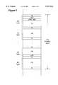
- Each sectoras illustrated in FIG. 4, contains 2064 bytes of data and codes in the following segments:
- each sectormay be divided into 12 rows of 172 bytes each, the total of which is 2064 bytes of information, of which 2048 are data.
- the concept of a data sectorremains in DVD technology.
- the ID(e.g., logical sector address) may be first determined, and then error detection/correction IED is calculated.
- error detection and correction techniquesare well known in the art (e.g., hamming codes, and the like) and are not necessary for a complete understanding of the present invention.
- the IEDsix bytes are reserved for proprietary copyright information in the CPR-MAI field.
- Error detection code EDCmay represent an error detection code for data within the sector illustrated in FIG. 4. For purposes of illustration, Error Correction Codes (ECC) is not illustrated in FIG. 4.
- the DATA portionmay then be scrambled. At this point, actual data may not have been written to a DVD, but merely formatted and stored in preparation for writing (or manufacturing) a DVD.
- the non-DATA portions of the sector illustrated in FIG. 4are not scrambled, only the DATA portion.
- FIG. 2is a simplified schematic representation of a DATA scrambler.
- Datais scrambled on a byte-by-byte basis.
- Each byte from the 2048 bytes in the sector of FIG. 4is individually scrambled and then returned to its original location.
- Actual scramblingcomprises taking an individual byte of data and XORing the data with a predetermined pattern byte. To descramble the data, one need only XOR the scrambled data with the correct pattern to retrieve the unscrambled data.
- the data scramblerworks as follows.
- a starting "seed" of fifteen bitsis stored in a shift register 290.
- Other numbers of bitsmay be used, but for DVD data, fifteen bits has been chosen.
- the eight least significant bits (LSB), or bits r0 through r7 of the contents of shift register 290may be used to XOR with a particular data byte.
- the first data bytemay be XORed with the eight LSB of S -- REG -- HOLD -- HALF.
- the scrambler of FIG. 2After that, the scrambler of FIG. 2 generates a new pattern from the contents of shift register 290 as follows.
- the contents of shift registercontain fifteen bits, r 0 through r 14 .
- a new patternis generated by shifting the contents of shift register 290 and XORing bit r 14 with bit r 10 in XOR gate 280 and placing the contents in bit r 0 of shift register 290 as illustrated in FIG. 2. This shift and XOR operation may be performed eight times to generate a new scrambling pattern from the previous contents of shift register 290.
- each byteis scrambled, it is returned to its correct corresponding location in the sector of FIG. 4.
- Information indicating which of a number seed values is to be usedmay be dependent on the identification section ID. Thus, the seed value may change from sector to sector.
- error correction codeshave not been discussed for the sake of clarity and simplicity. However, in actual practice, once all sectors, or a number of sectors, have been formatted, and prior to byte scrambling, other types of error correction codes may be applied as illustrated in FIG. 3.
- FIG. 3is a diagram illustrating the data storage format for data in the buffer memory with parity information.
- Data from a number of sectorse.g., 16
- an error correction codecomprising outer and inner parity values (PO and PI).
- Outer and inner parity values PO and PImay then be interleaved with DATA (D1, D2, D3) within each sector.
- DATAD1, D2, D3
- Outer and inner parity values PO and PIare not scrambled or treated as regular data. Thus, once DATA has been assigned to individual sectors and scrambled, interleaved outer and inner parity values are calculated and assigned to each sector. DATA (but not outer and inner parity values PO and PI) are scrambled as discussed above. Before DATA is descrambled, parity values PO and PI are used to detect and correct errors in scrambled DATA.
- the descrambling device of the present inventionwill divert PI and PO data from the descrambler and store such data directly in the buffer if the host demands such data.
- the descrambling circuitmay distinguish between scrambled DATA and PI and PO information.
- FIG. 2may be reproduced anywhere, so long as a user has the correct seed and combinational logic.
- a simple descramblermay be built from FIG. 2 as well.
- such a descramblermay require up to eight clock cycles between descrambling each byte in order to generate a new descrambling pattern value using the shift and XOR operation outlined above.
- Such a techniquemay be undesirable when descrambling data in real-time.
- FIG. 1is a block diagram illustrating a DVD descrambler which may descramble DVD data on a byte-by-byte basis.
- Data from a DVDmay be initially stored in raw form in a DRAM buffer (not shown).
- Data from the DRAM buffermay be fed over Buffer Data Input bus (BDI) which may comprise a 16 bit wide bus.
- Latch 100may receive buffer data and latch 16 bits at the start of each sector in response to signal load -- ID0.
- Signal load -- ID0may be generated from the start of a sector or the end of a previous sector.
- BDIBuffer Data Input bus
- Bits 4 through 7 of the ID fieldare used to select one of sixteen seed values from look-up table (LUT) 110. Predetermined seed values are stored in LUT 110 according to the DVD specification.
- the output of LUT 110is the 15 bit SEED, which passes to MUX 120.
- signal LOAD SEEDswitches MUX 120 to load the 15 bit SEED value to S-REG 130. Thereafter, the value loaded into S-REG 130 is fed back as will be discussed in more detail below.
- the fifteen bits of the SEEDare loaded as bits r0 through r 14 .
- CD-ROM and CD audiomost things are happening in a serial fashion.
- DSPDigital Signal Processor
- S-REG 130, XOR gate 140 and S-REG-HOLD-HALF register 150together performs a "flash" pattern generation using a shift and XOR operation to generate a descrambling pattern in one cycle.
- S-REG 130operates on a half-clock cycle basis. Within one clock cycle, S-REG 130, S-REG-HOLD-HALF register 150, and XOR gate 140 perform the equivalent of eight place shifts and eight simultaneous XOR operations. As there are 15 bits in the pattern value, it is possible to obtain the next subsequent pattern without waiting for individual shift operations to be completed.
- the seven LSB of S-REG 130are shifted into the seven Most Significant Bits (MSBs) of S-REG-HOLD-HALF register 150.
- the eight MSB of S-REG 130are XORed together as follows and stored in the eight LSB of S-REG-HOLD-HALF register 150 according to the following equations:
- a two clock cycle buffermay be used. Every two clock cycles, the buffer is accessed once to retrieve 16 bits. However, the apparatus of FIG. 1 produces one byte of pattern at a time. One byte of pattern is needed to generate one descrambled byte in one clock cycle so that a second clock cycle may generate a second byte, to form a word.
- the present inventionuses a half-clock to temporarily store that pattern information in S-REG-HOLD-HALF register 150.
- S-REG-HOLD-HALF register 150When shifting the contents of S-REG 130, data is not destroyed and the shifted pattern may be retained to generate the next byte of pattern data.
- S-REG-HOLD-HALF register 150holds the new pattern and then sends it back to MUX 120.
- One input of MUX 120is taking the new shifted pattern, while the other leg of MUX 120 is taking the SEED.
- the SEEDis loaded into S-REG 130.
- S-REG 130is updated with new pattern data.
- S-REG-HOLD-HALF register 150The output of S-REG-HOLD-HALF register 150 is fed to latches 160 and 170.
- Latch 160will latch the eight LSB of the contents of S-REG-HOLD-HALF for a lower byte of buffer data BDI 7:0!.
- Latch 170will latch the eight LSB of the contents of S-REG-HOLD-HALF for an upper byte of buffer data BDI 15:8!.
- XOR gate 180will XOR eight bits of pattern data from latch 160 with a lower byte of buffer data BDI 7:0!.
- XOR gate 190will XOR eight bits of pattern data from latch 170 with an upper byte of buffer data BDI 15:8!.
- the resulting descrambled datawill be selectively stored in Host FIFO 220 in corresponding low and high bytes.
- MUXES 200 and 210are provided to allow data from buffer data interface bus BDI to bypass the descrambling process.
- inner and outer parity information PI and POare interleaved with DATA in each sector.
- Signal DVD-dataindicates that data from buffer data interface bus BDI is in fact DATA and not parity information PI or PO, and switches XORed data into Host FIFO 220. If signal DVD-data indicates that data from buffer data interface BDI is PI or PO data, that data is switched directly to Host FIFO 220 without being XORed.
- the apparatus of FIG. 1may use two clock cycles to process one 16-bit word of data, providing adequate breathing room to process one byte in one clock cycle. A second clock cycle is used to process the high byte. Although the apparatus of FIG. 1 may be adequate for processing DVD data, in the preferred embodiment, it may be desirable to change to a different buffer access scheme, in which everything happens in one clock cycle.
- FIG. 5is a block diagram illustrating a DVD descrambler of the preferred embodiment which may descramble DVD data on a word-by-word basis.
- the apparatus of FIG. 5is similar to that in FIG. 1, except that the data path for the pattern has been expanded to sixteen bits, and sixteen bits of DATA from buffer data interface bus BDI are XORed in XOR gate 500 to descramble DATA.
- RTLRegister Transfer Logic
- XOR gate 140has been replaced by Register Transfer Logic (RTL) 540 which operates according to equations 9-39 below.
- RTL 540receives all fifteen bytes of pattern data from S-REG 130 and outputs two bytes of pattern data SP 15:0! to S-REG-HOLD-HALF register 150 which has been expanded to sixteen bits accordingly.
- Pattern data SP 15:0!represents two sequential bytes of pattern data for descrambling two successive bytes of DATA.
- RTL 540also outputs 15 bits of revised pattern data representing a revised 15 bit pattern corresponding to the high byte of a word. This 15 bit pattern is then fed back through S-REG 130 to generate the next two bytes of pattern data according to equations 9-39.
- Equation 9-39In this table, S 1 and S 2 represent the equivalent of a first and second shift (e.g., low byte and high byte), respectively, in a byte-by-byte descrambling system such as that illustrated in FIG. 1. As can be noted from equations 9-39, it is not necessary to perform the first shift in order to calculate values for the second shift. Thus, a combination logic circuit or the like may be readily constructed to generate the values of equations 9-39 in one clock cycle. In the preferred embodiment, a register transfer logic may be employed to implement equations 9-39.
- Scrambler Pattern SD 15:0!equals the shift patterns S1 7:0! and S2 7:0! concatenated into one word. Scrambler pattern SD 15:0! may then be used to XOR with one word of DATA to descramble DATA on a word-by-word basis.
- datamay be output to the host buffer and also to data sector EDC 230.
- Data sector EDC 230may perform a checksum, CRC or the like, to determine whether any errors have been introduced into sector data. If an error occurs, the sector may be re-read, processing may be halted, or other appropriate action taken.
- One advantage of the present inventionis that data is left untouched in the DRAM buffer, except when error correction occurs. Even when error correction occurs, only corrupted data is corrected, and the order of data is not altered. Raw (scrambled) data thus sits in the DRAM buffer waiting to be grabbed, to run through the circuit of FIGS. 1 or 5.
Landscapes
- Engineering & Computer Science (AREA)
- Signal Processing (AREA)
- Multimedia (AREA)
- Signal Processing For Digital Recording And Reproducing (AREA)
Abstract
Description
______________________________________Segment Bytes Description______________________________________ID 4 IdentificationIED 2 ID error detection (detection & correction for ID)CPR-MAI 6 Copyright Management InformationDATA 2048 DataEDC 4 Error Detection Code (for DATA)______________________________________
s.sub.1 7!=r.sub.14 ⊕r.sub.10 (1)
s.sub.1 6!=r.sub.13 ⊕r.sub.9 (2)
s.sub.1 5!=r.sub.12 ⊕r.sub.8 (3)
s.sub.1 4!=r.sub.11 ⊕r.sub.7 (4)
s.sub.1 3!=r.sub.10 ⊕r.sub.6 (5)
s.sub.1 2!=r.sub.9 ⊕r.sub.5 (6)
s.sub.1 1!=r.sub.8 ⊕r.sub.4 (7)
s.sub.1 0!=r.sub.7 ⊕r.sub.3 (8)
s.sub.1 14!=r.sub.6 (9)
s.sub.1 13!=r.sub.5 (10)
s.sub.1 12!=r.sub.4 (11)
s.sub.1 11!=r.sub.3 (12)
s.sub.1 10!=r.sub.2 (13)
s.sub.1 9!=r.sub.1 (14)
s.sub.1 8!=r.sub.0 (15)
s.sub.1 7!=r.sub.14 ⊕r.sub.10 (16)
s.sub.1 6!=r.sub.13 ⊕r.sub.9 (17)
s.sub.1 5!=r.sub.12 ⊕r.sub.8 (18)
s.sub.1 4!=r.sub.11 ⊕r.sub.7 (19)
s.sub.1 3!=r.sub.10 ⊕r.sub.6 (20)
s.sub.1 2!=r.sub.9 ⊕r.sub.5 (21)
s.sub.1 1!=r.sub.8 ⊕r.sub.4 (22)
s.sub.1 0!=r.sub.7 ⊕r.sub.3 (23)
s.sub.2 14!=s.sub.1 6!=r.sub.13 ⊕r.sub.9 (24)
s.sub.2 13!=s.sub.1 5!=r.sub.12 ⊕r.sub.8 (25)
s.sub.2 12!=s.sub.1 4!=r.sub.11 ⊕r.sub.7 (26)
s.sub.2 11!=s.sub.1 3!=r.sub.10 ⊕r.sub.6 (27)
s.sub.2 10!=s.sub.1 2!=r.sub.9 ⊕r.sub.5 (28)
s.sub.2 9!=s.sub.1 1!=r.sub.8 ⊕r.sub.4 (29)
s.sub.2 8!=s.sub.1 0!=r.sub.14 ⊕r.sub.10 (30)
s.sub.2 7!=s.sub.1 14!⊕s.sub.1 10!=r.sub.6 ⊕r.sub.2(31)
s.sub.2 6!=s.sub.1 13!⊕s.sub.1 9!=r.sub.5 ⊕r.sub.1(32)
s.sub.2 5!=s.sub.1 12!⊕s.sub.1 8!=r.sub.4 ⊕r.sub.0(33)
s.sub.2 4!=s.sub.1 11!⊕s.sub.1 7!=r.sub.3 ⊕r.sub.14 ⊕r.sub.10(34)
s.sub.2 3!=s.sub.1 10!⊕s.sub.1 6!=r.sub.2 ⊕r.sub.13 ⊕r.sub.9(35)
s.sub.2 2!=s.sub.1 9!⊕s.sub.1 5!=r.sub.1 ⊕r.sub.12 ⊕r.sub.8( 36)
s.sub.2 1!=s.sub.1 8!⊕s.sub.1 4!=r.sub.0 ⊕r.sub.11 ⊕r.sub.7( 37)
s.sub.2 0!=s.sub.1 7!⊕s.sub.1 3!=r.sub.14 ⊕r.sub.10 ⊕r.sub.10 ⊕r.sub.6 (38)
SD 15:0!=s.sub.2 7:0!&s1 7:0! (39)
Claims (16)
Priority Applications (1)
| Application Number | Priority Date | Filing Date | Title |
|---|---|---|---|
| US08/845,725US5917914A (en) | 1997-04-24 | 1997-04-24 | DVD data descrambler for host interface and MPEG interface |
Applications Claiming Priority (1)
| Application Number | Priority Date | Filing Date | Title |
|---|---|---|---|
| US08/845,725US5917914A (en) | 1997-04-24 | 1997-04-24 | DVD data descrambler for host interface and MPEG interface |
Publications (1)
| Publication Number | Publication Date |
|---|---|
| US5917914Atrue US5917914A (en) | 1999-06-29 |
Family
ID=25295947
Family Applications (1)
| Application Number | Title | Priority Date | Filing Date |
|---|---|---|---|
| US08/845,725Expired - LifetimeUS5917914A (en) | 1997-04-24 | 1997-04-24 | DVD data descrambler for host interface and MPEG interface |
Country Status (1)
| Country | Link |
|---|---|
| US (1) | US5917914A (en) |
Cited By (32)
| Publication number | Priority date | Publication date | Assignee | Title |
|---|---|---|---|---|
| US6119259A (en)* | 1997-05-09 | 2000-09-12 | Samsung Electronics Co., Ltd. | Method and apparatus of improving reliability of a descrambling operation in a DVD player |
| US6167551A (en)* | 1998-07-29 | 2000-12-26 | Neomagic Corp. | DVD controller with embedded DRAM for ECC-block buffering |
| WO2001005075A1 (en)* | 1999-07-13 | 2001-01-18 | Microsoft Corporation | Improved audio watermarking with covert channel and permutations |
| US20020001261A1 (en)* | 2000-04-21 | 2002-01-03 | Yoshinori Matsui | Data playback apparatus |
| US20020037080A1 (en)* | 2000-08-08 | 2002-03-28 | Yukari Katayama | Optical disk apparatus and data randomizing method using for optical disk apparatus |
| US6512883B2 (en)* | 1997-06-28 | 2003-01-28 | Samsung Electronics Co., Ltd. | Control apparatus and method for reproducing data from a digital video disk at high speed |
| US20030044005A1 (en)* | 2001-08-15 | 2003-03-06 | Lee Eugene W. | Data scrambler |
| US20030135798A1 (en)* | 2001-12-13 | 2003-07-17 | Yukari Katayama | Optical disk device and data randomizing method for optical disk device |
| US20040059581A1 (en)* | 1999-05-22 | 2004-03-25 | Darko Kirovski | Audio watermarking with dual watermarks |
| US20040067046A1 (en)* | 2002-10-07 | 2004-04-08 | Samsung Electronics Co., Ltd. | Apparatus and method for scrambling and descrambling data wordwise in optical disk system |
| US6738744B2 (en) | 2000-12-08 | 2004-05-18 | Microsoft Corporation | Watermark detection via cardinality-scaled correlation |
| US6754784B1 (en) | 2000-02-01 | 2004-06-22 | Cirrus Logic, Inc. | Methods and circuits for securing encached information |
| US20040204943A1 (en)* | 1999-07-13 | 2004-10-14 | Microsoft Corporation | Stealthy audio watermarking |
| US20050055214A1 (en)* | 2003-07-15 | 2005-03-10 | Microsoft Corporation | Audio watermarking with dual watermarks |
| US20050053240A1 (en)* | 2003-09-09 | 2005-03-10 | Peter Lablans | Ternary and higher multi-value digital scramblers/descramblers |
| US20050184888A1 (en)* | 2004-02-25 | 2005-08-25 | Peter Lablans | Generation and detection of non-binary digital sequences |
| US20050185796A1 (en)* | 2004-02-25 | 2005-08-25 | Peter Lablans | Ternary and multi-value digital signal scramblers, descramblers and sequence generators |
| US20050194993A1 (en)* | 2004-02-25 | 2005-09-08 | Peter Lablans | Single and composite binary and multi-valued logic functions from gates and inverters |
| US20060021003A1 (en)* | 2004-06-23 | 2006-01-26 | Janus Software, Inc | Biometric authentication system |
| US20060031278A1 (en)* | 2004-08-07 | 2006-02-09 | Peter Lablans | Multi-value digital calculating circuits, including multipliers |
| US7134039B2 (en) | 2004-07-06 | 2006-11-07 | Magnum Semiconductor, Inc. | Recovery of real-time video data after power loss |
| US20070110229A1 (en)* | 2004-02-25 | 2007-05-17 | Ternarylogic, Llc | Ternary and Multi-Value Digital Signal Scramblers, Descramblers and Sequence of Generators |
| US20090113269A1 (en)* | 2005-09-26 | 2009-04-30 | Daigo Senoo | Data descrambling apparatus and data descrambling method |
| US20090128190A1 (en)* | 2004-02-25 | 2009-05-21 | Peter Lablans | Implementing Logic Functions with Non-Magnitude Based Physical Phenomena |
| US7548092B2 (en) | 2004-02-25 | 2009-06-16 | Ternarylogic Llc | Implementing logic functions with non-magnitude based physical phenomena |
| US20100158366A1 (en)* | 2006-02-15 | 2010-06-24 | Terry Scott Brown | Continuous Color Grading Technique |
| US20100164548A1 (en)* | 2004-09-08 | 2010-07-01 | Ternarylogic Llc | Implementing Logic Functions With Non-Magnitude Based Physical Phenomena |
| US20100300271A1 (en)* | 2009-05-27 | 2010-12-02 | Microsoft Corporation | Detecting Beat Information Using a Diverse Set of Correlations |
| US20110064214A1 (en)* | 2003-09-09 | 2011-03-17 | Ternarylogic Llc | Methods and Apparatus in Alternate Finite Field Based Coders and Decoders |
| WO2011084214A3 (en)* | 2009-12-17 | 2011-09-01 | Intel Corporation | Method and apparatus for performing a shift and exclusive or operation in a single instruction |
| US8374289B2 (en) | 2004-02-25 | 2013-02-12 | Ternarylogic Llc | Generation and detection of non-binary digital sequences |
| US8577026B2 (en) | 2010-12-29 | 2013-11-05 | Ternarylogic Llc | Methods and apparatus in alternate finite field based coders and decoders |
Citations (10)
| Publication number | Priority date | Publication date | Assignee | Title |
|---|---|---|---|---|
| US4639548A (en)* | 1984-04-03 | 1987-01-27 | Nec Corporation | Digital communication system including an error correcting encoder/decoder and a scrambler/descrambler |
| US4669118A (en)* | 1984-02-02 | 1987-05-26 | Siemens Aktiengesellschaft | Self-synchronizing descrambler |
| US4668103A (en)* | 1982-04-30 | 1987-05-26 | Wilson William J | Polygraphic encryption-decryption communications system |
| US5016275A (en)* | 1988-10-28 | 1991-05-14 | International Business Machines Corporation | Buffered encryption/decryption |
| US5285497A (en)* | 1993-04-01 | 1994-02-08 | Scientific Atlanta | Methods and apparatus for scrambling and unscrambling compressed data streams |
| US5365589A (en)* | 1992-02-07 | 1994-11-15 | Gutowitz Howard A | Method and apparatus for encryption, decryption and authentication using dynamical systems |
| US5386469A (en)* | 1993-08-05 | 1995-01-31 | Zilog, Inc. | Firmware encryption for microprocessor/microcomputer |
| US5406627A (en)* | 1990-08-06 | 1995-04-11 | Nec Home Electronics, Ltd. | Digital data cryptographic system |
| US5535327A (en)* | 1994-06-23 | 1996-07-09 | Oak Technology, Inc. | Method and apparatus for communicating formatted data from a mass storage device to a host computer |
| US5581715A (en)* | 1994-06-22 | 1996-12-03 | Oak Technologies, Inc. | IDE/ATA CD drive controller having a digital signal processor interface, dynamic random access memory, data error detection and correction, and a host interface |
- 1997
- 1997-04-24USUS08/845,725patent/US5917914A/ennot_activeExpired - Lifetime
Patent Citations (11)
| Publication number | Priority date | Publication date | Assignee | Title |
|---|---|---|---|---|
| US4668103A (en)* | 1982-04-30 | 1987-05-26 | Wilson William J | Polygraphic encryption-decryption communications system |
| US4669118A (en)* | 1984-02-02 | 1987-05-26 | Siemens Aktiengesellschaft | Self-synchronizing descrambler |
| US4639548A (en)* | 1984-04-03 | 1987-01-27 | Nec Corporation | Digital communication system including an error correcting encoder/decoder and a scrambler/descrambler |
| US5016275A (en)* | 1988-10-28 | 1991-05-14 | International Business Machines Corporation | Buffered encryption/decryption |
| US5406627A (en)* | 1990-08-06 | 1995-04-11 | Nec Home Electronics, Ltd. | Digital data cryptographic system |
| US5406627B1 (en)* | 1990-08-06 | 1997-02-04 | Nippon Denki Home Electronics | System and method for transmitting entertainment information to authorized ones of plural receivers |
| US5365589A (en)* | 1992-02-07 | 1994-11-15 | Gutowitz Howard A | Method and apparatus for encryption, decryption and authentication using dynamical systems |
| US5285497A (en)* | 1993-04-01 | 1994-02-08 | Scientific Atlanta | Methods and apparatus for scrambling and unscrambling compressed data streams |
| US5386469A (en)* | 1993-08-05 | 1995-01-31 | Zilog, Inc. | Firmware encryption for microprocessor/microcomputer |
| US5581715A (en)* | 1994-06-22 | 1996-12-03 | Oak Technologies, Inc. | IDE/ATA CD drive controller having a digital signal processor interface, dynamic random access memory, data error detection and correction, and a host interface |
| US5535327A (en)* | 1994-06-23 | 1996-07-09 | Oak Technology, Inc. | Method and apparatus for communicating formatted data from a mass storage device to a host computer |
Cited By (75)
| Publication number | Priority date | Publication date | Assignee | Title |
|---|---|---|---|---|
| US6119259A (en)* | 1997-05-09 | 2000-09-12 | Samsung Electronics Co., Ltd. | Method and apparatus of improving reliability of a descrambling operation in a DVD player |
| US6512883B2 (en)* | 1997-06-28 | 2003-01-28 | Samsung Electronics Co., Ltd. | Control apparatus and method for reproducing data from a digital video disk at high speed |
| US6167551A (en)* | 1998-07-29 | 2000-12-26 | Neomagic Corp. | DVD controller with embedded DRAM for ECC-block buffering |
| US6952774B1 (en) | 1999-05-22 | 2005-10-04 | Microsoft Corporation | Audio watermarking with dual watermarks |
| US20040059581A1 (en)* | 1999-05-22 | 2004-03-25 | Darko Kirovski | Audio watermarking with dual watermarks |
| US7197368B2 (en) | 1999-05-22 | 2007-03-27 | Microsoft Corporation | Audio watermarking with dual watermarks |
| US7266697B2 (en) | 1999-07-13 | 2007-09-04 | Microsoft Corporation | Stealthy audio watermarking |
| US7543148B1 (en) | 1999-07-13 | 2009-06-02 | Microsoft Corporation | Audio watermarking with covert channel and permutations |
| US7020285B1 (en) | 1999-07-13 | 2006-03-28 | Microsoft Corporation | Stealthy audio watermarking |
| US20050108542A1 (en)* | 1999-07-13 | 2005-05-19 | Microsoft Corporation | Watermarking with covert channel and permutations |
| US7552336B2 (en) | 1999-07-13 | 2009-06-23 | Microsoft Corporation | Watermarking with covert channel and permutations |
| WO2001005075A1 (en)* | 1999-07-13 | 2001-01-18 | Microsoft Corporation | Improved audio watermarking with covert channel and permutations |
| US20040204943A1 (en)* | 1999-07-13 | 2004-10-14 | Microsoft Corporation | Stealthy audio watermarking |
| US6754784B1 (en) | 2000-02-01 | 2004-06-22 | Cirrus Logic, Inc. | Methods and circuits for securing encached information |
| US7123815B2 (en) | 2000-04-21 | 2006-10-17 | Matsushita Electric Industrial Co., Ltd. | Data playback apparatus |
| EP1148505A3 (en)* | 2000-04-21 | 2002-03-27 | Matsushita Electric Industrial Co., Ltd. | Data playback apparatus |
| US20020001261A1 (en)* | 2000-04-21 | 2002-01-03 | Yoshinori Matsui | Data playback apparatus |
| US20020037080A1 (en)* | 2000-08-08 | 2002-03-28 | Yukari Katayama | Optical disk apparatus and data randomizing method using for optical disk apparatus |
| US7155015B2 (en)* | 2000-08-08 | 2006-12-26 | Hitachi, Ltd. | Optical disk apparatus and data randomizing method using for optical disk apparatus |
| US6738744B2 (en) | 2000-12-08 | 2004-05-18 | Microsoft Corporation | Watermark detection via cardinality-scaled correlation |
| US20030044005A1 (en)* | 2001-08-15 | 2003-03-06 | Lee Eugene W. | Data scrambler |
| US20030135798A1 (en)* | 2001-12-13 | 2003-07-17 | Yukari Katayama | Optical disk device and data randomizing method for optical disk device |
| US20060248427A1 (en)* | 2001-12-13 | 2006-11-02 | Yukari Katayama | Optical disk device and data randomizing method for optical disk drive |
| US7248697B2 (en) | 2002-10-07 | 2007-07-24 | Samsung Electronics, Co., Ltd. | Apparatus and method for scrambling and descrambling data wordwise in optical disk system |
| KR100510492B1 (en)* | 2002-10-07 | 2005-08-26 | 삼성전자주식회사 | Word-wide scrambing/descrambling apparatus in optical disc system and Method there-of |
| US20040067046A1 (en)* | 2002-10-07 | 2004-04-08 | Samsung Electronics Co., Ltd. | Apparatus and method for scrambling and descrambling data wordwise in optical disk system |
| US7206649B2 (en) | 2003-07-15 | 2007-04-17 | Microsoft Corporation | Audio watermarking with dual watermarks |
| US20050055214A1 (en)* | 2003-07-15 | 2005-03-10 | Microsoft Corporation | Audio watermarking with dual watermarks |
| US7864079B1 (en) | 2003-09-09 | 2011-01-04 | Ternarylogic Llc | Ternary and higher multi-value digital scramblers/descramblers |
| US20090060202A1 (en)* | 2003-09-09 | 2009-03-05 | Peter Lablans | Ternary and Higher Multi-Value Digital Scramblers/Descramblers |
| US7002490B2 (en) | 2003-09-09 | 2006-02-21 | Ternarylogic Llc | Ternary and higher multi-value digital scramblers/descramblers |
| US20050053240A1 (en)* | 2003-09-09 | 2005-03-10 | Peter Lablans | Ternary and higher multi-value digital scramblers/descramblers |
| US20100322414A1 (en)* | 2003-09-09 | 2010-12-23 | Ternarylogic Llc | Ternary and higher multi-value digital scramblers/descramblers |
| US20050084111A1 (en)* | 2003-09-09 | 2005-04-21 | Peter Lablans | Ternary and higher multi-value digital scramblers/descramblers |
| US20110064214A1 (en)* | 2003-09-09 | 2011-03-17 | Ternarylogic Llc | Methods and Apparatus in Alternate Finite Field Based Coders and Decoders |
| US7505589B2 (en) | 2003-09-09 | 2009-03-17 | Temarylogic, Llc | Ternary and higher multi-value digital scramblers/descramblers |
| US8589466B2 (en) | 2004-02-25 | 2013-11-19 | Ternarylogic Llc | Ternary and multi-value digital signal scramblers, decramblers and sequence generators |
| US7218144B2 (en) | 2004-02-25 | 2007-05-15 | Ternarylogic Llc | Single and composite binary and multi-valued logic functions from gates and inverters |
| US7355444B2 (en) | 2004-02-25 | 2008-04-08 | Ternarylogic Llc | Single and composite binary and multi-valued logic functions from gates and inverters |
| US20050194993A1 (en)* | 2004-02-25 | 2005-09-08 | Peter Lablans | Single and composite binary and multi-valued logic functions from gates and inverters |
| US20070152710A1 (en)* | 2004-02-25 | 2007-07-05 | Peter Lablans | Single and composite binary and multi-valued logic functions from gates and inverters |
| US20070110229A1 (en)* | 2004-02-25 | 2007-05-17 | Ternarylogic, Llc | Ternary and Multi-Value Digital Signal Scramblers, Descramblers and Sequence of Generators |
| US20090128190A1 (en)* | 2004-02-25 | 2009-05-21 | Peter Lablans | Implementing Logic Functions with Non-Magnitude Based Physical Phenomena |
| US20050184888A1 (en)* | 2004-02-25 | 2005-08-25 | Peter Lablans | Generation and detection of non-binary digital sequences |
| US7548092B2 (en) | 2004-02-25 | 2009-06-16 | Ternarylogic Llc | Implementing logic functions with non-magnitude based physical phenomena |
| US20050185796A1 (en)* | 2004-02-25 | 2005-08-25 | Peter Lablans | Ternary and multi-value digital signal scramblers, descramblers and sequence generators |
| US20110170697A1 (en)* | 2004-02-25 | 2011-07-14 | Ternarylogic Llc | Ternary and Multi-Value Digital Signal Scramblers, Decramblers and Sequence Generators |
| US7580472B2 (en) | 2004-02-25 | 2009-08-25 | Ternarylogic Llc | Generation and detection of non-binary digital sequences |
| US7643632B2 (en) | 2004-02-25 | 2010-01-05 | Ternarylogic Llc | Ternary and multi-value digital signal scramblers, descramblers and sequence generators |
| US7696785B2 (en) | 2004-02-25 | 2010-04-13 | Ternarylogic Llc | Implementing logic functions with non-magnitude based physical phenomena |
| US8374289B2 (en) | 2004-02-25 | 2013-02-12 | Ternarylogic Llc | Generation and detection of non-binary digital sequences |
| US20060021003A1 (en)* | 2004-06-23 | 2006-01-26 | Janus Software, Inc | Biometric authentication system |
| US7134039B2 (en) | 2004-07-06 | 2006-11-07 | Magnum Semiconductor, Inc. | Recovery of real-time video data after power loss |
| US7562106B2 (en) | 2004-08-07 | 2009-07-14 | Ternarylogic Llc | Multi-value digital calculating circuits, including multipliers |
| US20060031278A1 (en)* | 2004-08-07 | 2006-02-09 | Peter Lablans | Multi-value digital calculating circuits, including multipliers |
| US20100164548A1 (en)* | 2004-09-08 | 2010-07-01 | Ternarylogic Llc | Implementing Logic Functions With Non-Magnitude Based Physical Phenomena |
| US20090113269A1 (en)* | 2005-09-26 | 2009-04-30 | Daigo Senoo | Data descrambling apparatus and data descrambling method |
| US20100158366A1 (en)* | 2006-02-15 | 2010-06-24 | Terry Scott Brown | Continuous Color Grading Technique |
| US8077967B2 (en)* | 2006-02-15 | 2011-12-13 | Thomson Licensing | Continuous color grading technique |
| US8878041B2 (en) | 2009-05-27 | 2014-11-04 | Microsoft Corporation | Detecting beat information using a diverse set of correlations |
| US20100300271A1 (en)* | 2009-05-27 | 2010-12-02 | Microsoft Corporation | Detecting Beat Information Using a Diverse Set of Correlations |
| JP2014160500A (en)* | 2009-12-17 | 2014-09-04 | Intel Corp | Method and apparatus for performing shift and exclusive-or operation in single instruction |
| US9495166B2 (en) | 2009-12-17 | 2016-11-15 | Intel Corporation | Method and apparatus for performing a shift and exclusive or operation in a single instruction |
| JP2012530978A (en)* | 2009-12-17 | 2012-12-06 | インテル・コーポレーション | Method and apparatus for performing shift and exclusive OR operations with a single instruction |
| GB2483575A (en)* | 2009-12-17 | 2012-03-14 | Intel Corp | Method and apparatus for performing a shift and exclusive or operation in a single instruction |
| JP2014194825A (en)* | 2009-12-17 | 2014-10-09 | Intel Corp | Method and apparatus for performing shift and exclusive OR operations with a single instruction |
| WO2011084214A3 (en)* | 2009-12-17 | 2011-09-01 | Intel Corporation | Method and apparatus for performing a shift and exclusive or operation in a single instruction |
| JP2015164061A (en)* | 2009-12-17 | 2015-09-10 | インテル・コーポレーション | Method and apparatus for performing shift-and-exclusive OR operation with a single instruction |
| US10684855B2 (en) | 2009-12-17 | 2020-06-16 | Intel Corporation | Method and apparatus for performing a shift and exclusive or operation in a single instruction |
| US9495165B2 (en) | 2009-12-17 | 2016-11-15 | Intel Corporation | Method and apparatus for performing a shift and exclusive or operation in a single instruction |
| US9501281B2 (en) | 2009-12-17 | 2016-11-22 | Intel Corporation | Method and apparatus for performing a shift and exclusive or operation in a single instruction |
| US9747105B2 (en) | 2009-12-17 | 2017-08-29 | Intel Corporation | Method and apparatus for performing a shift and exclusive or operation in a single instruction |
| JP2017152016A (en)* | 2009-12-17 | 2017-08-31 | インテル・コーポレーション | System for performing shift and exclusive or operation in single instruction |
| GB2483575B (en)* | 2009-12-17 | 2017-11-01 | Intel Corp | Method and apparatus for performing a shift and exclusive or operation in a single instruction |
| US8577026B2 (en) | 2010-12-29 | 2013-11-05 | Ternarylogic Llc | Methods and apparatus in alternate finite field based coders and decoders |
Similar Documents
| Publication | Publication Date | Title |
|---|---|---|
| US5917914A (en) | DVD data descrambler for host interface and MPEG interface | |
| US6003151A (en) | Error correction and detection system for mass storage controller | |
| US5805799A (en) | Data integrity and cross-check code with logical block address | |
| US4667326A (en) | Method and apparatus for error detection and correction in systems comprising floppy and/or hard disk drives | |
| US6158038A (en) | Method and apparatus for correcting data errors | |
| CA1287166C (en) | Apparatus for recording and reproducing data | |
| US6445795B1 (en) | Data recording method and apparatus, data record medium and data reproducing method and apparatus | |
| US5996105A (en) | ECC system employing a data buffer for storing codeword data and a syndrome buffer for storing error syndromes | |
| US6363511B1 (en) | Device and method for decoding data streams from storage media | |
| US8171373B2 (en) | Coding circuit for recording data on DVD disk | |
| US20020083394A1 (en) | Method and apparatus for data reproduction | |
| US8281225B2 (en) | Digital data coding and recording apparatus, and method of using the same | |
| JP2000165259A (en) | Data decoding processor and its method | |
| US5717535A (en) | Block address integrity check for storage medium | |
| US7092979B1 (en) | Random data generator and scrambler using the same, and method therefore | |
| US8102996B2 (en) | Scrambler, descrambler and method, and disc apparatus | |
| US7607074B2 (en) | Error detecting code addition circuit, error detection circuit and method, and disc apparatus | |
| US6260169B1 (en) | Device and method for real time correction of row data from DVD media | |
| US5996107A (en) | Error correction decoder including an address generation circuit | |
| JP2008146828A (en) | Encode data encoding circuit for optical disk apparatus | |
| JP2001067815A (en) | Scrambler and scramble method | |
| JPS63197122A (en) | Error correcting and checking device | |
| JP3651332B2 (en) | Data processing method and data processing apparatus | |
| JP3279501B2 (en) | Error correction and error detection method for mass storage controller | |
| JP2002319233A (en) | Digital signal recording / reproducing device |
Legal Events
| Date | Code | Title | Description |
|---|---|---|---|
| AS | Assignment | Owner name:CIRRUS LOGIC, INC., CALIFORNIA Free format text:ASSIGNMENT OF ASSIGNORS INTEREST;ASSIGNORS:SHAW, YIH-SUEY;CHU, CHI-MING;REEL/FRAME:009421/0086 Effective date:19970423 | |
| STCF | Information on status: patent grant | Free format text:PATENTED CASE | |
| FPAY | Fee payment | Year of fee payment:4 | |
| AS | Assignment | Owner name:BROADCOM CORPORATION, CALIFORNIA Free format text:ASSIGNMENT OF ASSIGNORS INTEREST;ASSIGNOR:CIRRUS LOGIC INC;REEL/FRAME:014428/0418 Effective date:20040205 | |
| FPAY | Fee payment | Year of fee payment:8 | |
| FEPP | Fee payment procedure | Free format text:PAYOR NUMBER ASSIGNED (ORIGINAL EVENT CODE: ASPN); ENTITY STATUS OF PATENT OWNER: LARGE ENTITY | |
| AS | Assignment | Owner name:QUALCOMM INCORPORATED, CALIFORNIA Free format text:ASSIGNMENT OF ASSIGNORS INTEREST;ASSIGNOR:BROADCOM CORPORATION;REEL/FRAME:022973/0107 Effective date:20090610 Owner name:QUALCOMM INCORPORATED,CALIFORNIA Free format text:ASSIGNMENT OF ASSIGNORS INTEREST;ASSIGNOR:BROADCOM CORPORATION;REEL/FRAME:022973/0107 Effective date:20090610 | |
| FPAY | Fee payment | Year of fee payment:12 |