US5917757A - Flash memory with high speed erasing structure using thin oxide semiconductor devices - Google Patents
Flash memory with high speed erasing structure using thin oxide semiconductor devicesDownload PDFInfo
- Publication number
- US5917757A US5917757AUS08/882,558US88255897AUS5917757AUS 5917757 AUS5917757 AUS 5917757AUS 88255897 AUS88255897 AUS 88255897AUS 5917757 AUS5917757 AUS 5917757A
- Authority
- US
- United States
- Prior art keywords
- voltage
- voltage range
- wordline
- procedure
- flash memory
- Prior art date
- Legal status (The legal status is an assumption and is not a legal conclusion. Google has not performed a legal analysis and makes no representation as to the accuracy of the status listed.)
- Expired - Lifetime
Links
- 230000015654memoryEffects0.000titleclaimsabstractdescription90
- 239000004065semiconductorSubstances0.000titledescription3
- 238000000034methodMethods0.000claimsabstractdescription135
- 230000015556catabolic processEffects0.000claimsdescription37
- 230000008901benefitEffects0.000abstractdescription5
- 230000003247decreasing effectEffects0.000description17
- 230000005684electric fieldEffects0.000description16
- 230000006870functionEffects0.000description12
- 230000007423decreaseEffects0.000description9
- 238000006731degradation reactionMethods0.000description9
- 230000005532trappingEffects0.000description6
- 230000005641tunnelingEffects0.000description5
- 238000007667floatingMethods0.000description4
- 239000000758substrateSubstances0.000description4
- 238000012795verificationMethods0.000description4
- 238000005516engineering processMethods0.000description3
- 238000012986modificationMethods0.000description3
- 230000004048modificationEffects0.000description3
- 238000010348incorporationMethods0.000description2
- 230000008569processEffects0.000description2
- 238000012545processingMethods0.000description2
- LZIAMMQBHJIZAG-UHFFFAOYSA-N2-[di(propan-2-yl)amino]ethyl carbamimidothioateChemical compoundCC(C)N(C(C)C)CCSC(N)=NLZIAMMQBHJIZAG-UHFFFAOYSA-N0.000description1
- 238000013459approachMethods0.000description1
- 238000003491arrayMethods0.000description1
- 230000009286beneficial effectEffects0.000description1
- 238000004364calculation methodMethods0.000description1
- 230000008859changeEffects0.000description1
- 230000008878couplingEffects0.000description1
- 238000010168coupling processMethods0.000description1
- 238000005859coupling reactionMethods0.000description1
- 230000002950deficientEffects0.000description1
- 238000011982device technologyMethods0.000description1
- 238000010893electron trapMethods0.000description1
- 238000002474experimental methodMethods0.000description1
- 230000006872improvementEffects0.000description1
- 239000012535impuritySubstances0.000description1
- 238000004519manufacturing processMethods0.000description1
- 230000002093peripheral effectEffects0.000description1
- 230000002085persistent effectEffects0.000description1
- 230000002028prematureEffects0.000description1
- 230000027756respiratory electron transport chainEffects0.000description1
- 230000002459sustained effectEffects0.000description1
Images


Classifications
- G—PHYSICS
- G11—INFORMATION STORAGE
- G11C—STATIC STORES
- G11C16/00—Erasable programmable read-only memories
- G11C16/02—Erasable programmable read-only memories electrically programmable
- G11C16/06—Auxiliary circuits, e.g. for writing into memory
- G11C16/34—Determination of programming status, e.g. threshold voltage, overprogramming or underprogramming, retention
- G11C16/3418—Disturbance prevention or evaluation; Refreshing of disturbed memory data
- G11C16/3427—Circuits or methods to prevent or reduce disturbance of the state of a memory cell when neighbouring cells are read or written
- G—PHYSICS
- G05—CONTROLLING; REGULATING
- G05F—SYSTEMS FOR REGULATING ELECTRIC OR MAGNETIC VARIABLES
- G05F3/00—Non-retroactive systems for regulating electric variables by using an uncontrolled element, or an uncontrolled combination of elements, such element or such combination having self-regulating properties
- G05F3/02—Regulating voltage or current
- G05F3/08—Regulating voltage or current wherein the variable is DC
- G05F3/10—Regulating voltage or current wherein the variable is DC using uncontrolled devices with non-linear characteristics
- G05F3/16—Regulating voltage or current wherein the variable is DC using uncontrolled devices with non-linear characteristics being semiconductor devices
- G05F3/20—Regulating voltage or current wherein the variable is DC using uncontrolled devices with non-linear characteristics being semiconductor devices using diode- transistor combinations
- G—PHYSICS
- G11—INFORMATION STORAGE
- G11C—STATIC STORES
- G11C11/00—Digital stores characterised by the use of particular electric or magnetic storage elements; Storage elements therefor
- G11C11/56—Digital stores characterised by the use of particular electric or magnetic storage elements; Storage elements therefor using storage elements with more than two stable states represented by steps, e.g. of voltage, current, phase, frequency
- G11C11/5621—Digital stores characterised by the use of particular electric or magnetic storage elements; Storage elements therefor using storage elements with more than two stable states represented by steps, e.g. of voltage, current, phase, frequency using charge storage in a floating gate
- G11C11/5628—Programming or writing circuits; Data input circuits
- G11C11/5635—Erasing circuits
- G—PHYSICS
- G11—INFORMATION STORAGE
- G11C—STATIC STORES
- G11C11/00—Digital stores characterised by the use of particular electric or magnetic storage elements; Storage elements therefor
- G11C11/56—Digital stores characterised by the use of particular electric or magnetic storage elements; Storage elements therefor using storage elements with more than two stable states represented by steps, e.g. of voltage, current, phase, frequency
- G11C11/5621—Digital stores characterised by the use of particular electric or magnetic storage elements; Storage elements therefor using storage elements with more than two stable states represented by steps, e.g. of voltage, current, phase, frequency using charge storage in a floating gate
- G11C11/5642—Sensing or reading circuits; Data output circuits
- G—PHYSICS
- G11—INFORMATION STORAGE
- G11C—STATIC STORES
- G11C16/00—Erasable programmable read-only memories
- G11C16/02—Erasable programmable read-only memories electrically programmable
- G11C16/06—Auxiliary circuits, e.g. for writing into memory
- G11C16/08—Address circuits; Decoders; Word-line control circuits
- G—PHYSICS
- G11—INFORMATION STORAGE
- G11C—STATIC STORES
- G11C16/00—Erasable programmable read-only memories
- G11C16/02—Erasable programmable read-only memories electrically programmable
- G11C16/06—Auxiliary circuits, e.g. for writing into memory
- G11C16/10—Programming or data input circuits
- G—PHYSICS
- G11—INFORMATION STORAGE
- G11C—STATIC STORES
- G11C16/00—Erasable programmable read-only memories
- G11C16/02—Erasable programmable read-only memories electrically programmable
- G11C16/06—Auxiliary circuits, e.g. for writing into memory
- G11C16/10—Programming or data input circuits
- G11C16/14—Circuits for erasing electrically, e.g. erase voltage switching circuits
- G11C16/16—Circuits for erasing electrically, e.g. erase voltage switching circuits for erasing blocks, e.g. arrays, words, groups
- G—PHYSICS
- G11—INFORMATION STORAGE
- G11C—STATIC STORES
- G11C16/00—Erasable programmable read-only memories
- G11C16/02—Erasable programmable read-only memories electrically programmable
- G11C16/06—Auxiliary circuits, e.g. for writing into memory
- G11C16/30—Power supply circuits
- G—PHYSICS
- G11—INFORMATION STORAGE
- G11C—STATIC STORES
- G11C16/00—Erasable programmable read-only memories
- G11C16/02—Erasable programmable read-only memories electrically programmable
- G11C16/06—Auxiliary circuits, e.g. for writing into memory
- G11C16/34—Determination of programming status, e.g. threshold voltage, overprogramming or underprogramming, retention
- G11C16/3404—Convergence or correction of memory cell threshold voltages; Repair or recovery of overerased or overprogrammed cells
- G11C16/3409—Circuits or methods to recover overerased nonvolatile memory cells detected during erase verification, usually by means of a "soft" programming step
- G—PHYSICS
- G11—INFORMATION STORAGE
- G11C—STATIC STORES
- G11C16/00—Erasable programmable read-only memories
- G11C16/02—Erasable programmable read-only memories electrically programmable
- G11C16/06—Auxiliary circuits, e.g. for writing into memory
- G11C16/34—Determination of programming status, e.g. threshold voltage, overprogramming or underprogramming, retention
- G11C16/3418—Disturbance prevention or evaluation; Refreshing of disturbed memory data
- G11C16/3431—Circuits or methods to detect disturbed nonvolatile memory cells, e.g. which still read as programmed but with threshold less than the program verify threshold or read as erased but with threshold greater than the erase verify threshold, and to reverse the disturbance via a refreshing programming or erasing step
- G—PHYSICS
- G11—INFORMATION STORAGE
- G11C—STATIC STORES
- G11C16/00—Erasable programmable read-only memories
- G11C16/02—Erasable programmable read-only memories electrically programmable
- G11C16/06—Auxiliary circuits, e.g. for writing into memory
- G11C16/34—Determination of programming status, e.g. threshold voltage, overprogramming or underprogramming, retention
- G11C16/3436—Arrangements for verifying correct programming or erasure
- G11C16/344—Arrangements for verifying correct erasure or for detecting overerased cells
- G11C16/3445—Circuits or methods to verify correct erasure of nonvolatile memory cells
- G—PHYSICS
- G11—INFORMATION STORAGE
- G11C—STATIC STORES
- G11C5/00—Details of stores covered by group G11C11/00
- G11C5/14—Power supply arrangements, e.g. power down, chip selection or deselection, layout of wirings or power grids, or multiple supply levels
- G11C5/145—Applications of charge pumps; Boosted voltage circuits; Clamp circuits therefor
- G—PHYSICS
- G11—INFORMATION STORAGE
- G11C—STATIC STORES
- G11C8/00—Arrangements for selecting an address in a digital store
- G11C8/10—Decoders
- H—ELECTRICITY
- H02—GENERATION; CONVERSION OR DISTRIBUTION OF ELECTRIC POWER
- H02M—APPARATUS FOR CONVERSION BETWEEN AC AND AC, BETWEEN AC AND DC, OR BETWEEN DC AND DC, AND FOR USE WITH MAINS OR SIMILAR POWER SUPPLY SYSTEMS; CONVERSION OF DC OR AC INPUT POWER INTO SURGE OUTPUT POWER; CONTROL OR REGULATION THEREOF
- H02M3/00—Conversion of DC power input into DC power output
- H02M3/02—Conversion of DC power input into DC power output without intermediate conversion into AC
- H02M3/04—Conversion of DC power input into DC power output without intermediate conversion into AC by static converters
- H02M3/06—Conversion of DC power input into DC power output without intermediate conversion into AC by static converters using resistors or capacitors, e.g. potential divider
- H02M3/07—Conversion of DC power input into DC power output without intermediate conversion into AC by static converters using resistors or capacitors, e.g. potential divider using capacitors charged and discharged alternately by semiconductor devices with control electrode, e.g. charge pumps
- H02M3/073—Charge pumps of the Schenkel-type
- H—ELECTRICITY
- H03—ELECTRONIC CIRCUITRY
- H03K—PULSE TECHNIQUE
- H03K3/00—Circuits for generating electric pulses; Monostable, bistable or multistable circuits
- H03K3/02—Generators characterised by the type of circuit or by the means used for producing pulses
- H03K3/023—Generators characterised by the type of circuit or by the means used for producing pulses by the use of differential amplifiers or comparators, with internal or external positive feedback
- H03K3/0231—Astable circuits
- H—ELECTRICITY
- H10—SEMICONDUCTOR DEVICES; ELECTRIC SOLID-STATE DEVICES NOT OTHERWISE PROVIDED FOR
- H10B—ELECTRONIC MEMORY DEVICES
- H10B69/00—Erasable-and-programmable ROM [EPROM] devices not provided for in groups H10B41/00 - H10B63/00, e.g. ultraviolet erasable-and-programmable ROM [UVEPROM] devices
- G—PHYSICS
- G11—INFORMATION STORAGE
- G11C—STATIC STORES
- G11C2211/00—Indexing scheme relating to digital stores characterized by the use of particular electric or magnetic storage elements; Storage elements therefor
- G11C2211/56—Indexing scheme relating to G11C11/56 and sub-groups for features not covered by these groups
- G11C2211/562—Multilevel memory programming aspects
- G11C2211/5621—Multilevel programming verification
- G—PHYSICS
- G11—INFORMATION STORAGE
- G11C—STATIC STORES
- G11C2211/00—Indexing scheme relating to digital stores characterized by the use of particular electric or magnetic storage elements; Storage elements therefor
- G11C2211/56—Indexing scheme relating to G11C11/56 and sub-groups for features not covered by these groups
- G11C2211/564—Miscellaneous aspects
- G11C2211/5642—Multilevel memory with buffers, latches, registers at input or output
- G—PHYSICS
- G11—INFORMATION STORAGE
- G11C—STATIC STORES
- G11C2211/00—Indexing scheme relating to digital stores characterized by the use of particular electric or magnetic storage elements; Storage elements therefor
- G11C2211/56—Indexing scheme relating to G11C11/56 and sub-groups for features not covered by these groups
- G11C2211/564—Miscellaneous aspects
- G11C2211/5645—Multilevel memory with current-mirror arrangements
- G—PHYSICS
- G11—INFORMATION STORAGE
- G11C—STATIC STORES
- G11C2216/00—Indexing scheme relating to G11C16/00 and subgroups, for features not directly covered by these groups
- G11C2216/12—Reading and writing aspects of erasable programmable read-only memories
- G11C2216/18—Flash erasure of all the cells in an array, sector or block simultaneously
- G—PHYSICS
- G11—INFORMATION STORAGE
- G11C—STATIC STORES
- G11C8/00—Arrangements for selecting an address in a digital store
- G—PHYSICS
- G11—INFORMATION STORAGE
- G11C—STATIC STORES
- G11C8/00—Arrangements for selecting an address in a digital store
- G11C8/14—Word line organisation; Word line lay-out
Definitions
- the present inventionrelates to a flash memory with a high speed erasing structure and method.
- the inventionapplies selected voltages to the memory array wordlines, sourcelines or bitlines to increase the voltage differential across the tunnel oxide of cells to be erased in order to reduce erase time.
- the inventionpermits the peripheral devices to operate at a relatively high voltage range compared to conventional memories, while still using a thin oxide semiconductor device technology.
- Flash memoriesare becoming increasingly popular.
- many conventional flash memoriesemploy a large block erase limitation that is capable of erasing no less than a block of the memory at a time and re-programming the entire block with new data, even if only a small portion of the block needs to be re-programmed. Due to this relatively large re-programming technique, conventional flash memories are slow to respond and cannot achieve a large number of erase/program cycles due to the stress on the memory cells inherent in the erasing and programming cycles.
- flash transistor erasing timeis exponentially longer with a less negative erase voltage or a lower transistor threshold voltage. This is because the electric field in the transistor that causes the electron transfer to the floating gate will vary based on the applied voltages and the transistor threshold voltage. For example, the time required to erase a flash transistor will be longer if -9 V is applied to the gate rather than -10 V. And, for example, the time required to reduce a flash transistor threshold (Vt) from 2 V to 1 V is approximately ten times the time required to reduce the threshold from 3 V to 2 V. Some techniques of reducing this time are by applying a greater negative voltage (e.g. ⁇ -10 V) if the erase procedure is to remove electrons from the floating gate, or a greater positive voltage (e.g.
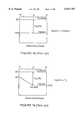
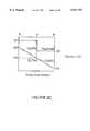
- FIG. 1Ashows a known technique that applies a fixed erase voltage of -10 V to the selected wordline (gate) for the entire erase procedure. Since the initial Vt is about 4 V greater than the final Vt after the completion of the erase procedure, the cell's tunnel oxide suffers the greatest electric stress at the beginning of the erase procedure, thus causing the hole trapping and oxide degradation. As a result, the flash transistor endurance is significantly reduced.
- FIG. 1BAnother known flash memory, described in U.S. Pat. No. 5,485,423 incorporated herein by reference and shown in FIG. 1B, employs a stepwise decreasing voltage to the selected wordline (transistor gates) in order to reduce the possibility of hole trapping in the tunnel oxide and oxide degradation.
- This techniquereduces the applied voltage in a stepwise fashion thereby reducing the high electrical field at the beginning of the erase procedure. Once the maximum negative voltage is achieved (e.g. -9.5 V), that voltage is applied until the erasure is complete. Although this technique significantly reduceas oxide degradation, the erase time is still exponentially long when the lower erase threshold voltage (Vt) is required.
- Vterase threshold voltage
- One feature common to the known flash memories of FIGS. 1A and 1Bis that the deselected wordlines and sourcelines maintain a fixed voltage (e.g. 0 V) during the erase procedure.
- the wordline drivers of these circuitsmay experience significant stress due to the large voltage differential between the driven lines and the non-driven lines if the voltages of wordlines or sourcelines are increased. Such stress can cause device junction breakdown and may cause premature degradation or failure of the wordline driver.
- the most negative or positive voltage of the selected wordlineis limited by the maximum tolerance of the breakdown voltage (BVDSS) of PMOS and NMOS devices in the X-decoder wordline drivers.
- the BVDSSis determined by the voltage drop between two power supplies connected to M20a, M20b and M21a, M21b as shown in FIGS. 5A-B.
- the voltage drop across the two power suppliesis equivalent to the voltage difference Vg(diff) between the selected wordline Vg(sel) and deselected wordline Vg(desel). If Vg(diff) exceeds the junction gated breakdown of the driver device (BVDSS), then large current will leak to the substrate until Vg(diff) drops to lower than (BVDSS).
- Thisis particularly relevant for thin oxide semiconductor devices which are conventionally used in flash memory circuits and where the maximum Vg(diff) is approximately +/-10 V.
- this voltage differenceis not sufficient to provide fast erasing at low threshold voltages below approximately 3 V.
- One further limitation of conventional flash memoriesis that the voltage across the cells' tunnel oxide is reduced when hole and electron trapping occurs after thousands of program and erase cycles.
- the wordline or sourceline voltageshave to be increased to compensate for the electric field drop induced by the trappings.
- Goals of the inventionare to overcome the identified problems and to provide a new technique to quickly erase selected portions of the flash memory and improve the life of the flash memory.
- a flash memory with a high speed erasing structureincludes a bank of flash transistors having a plurality of wordlines, a plurality of bitlines and a sourceline.
- a wordline decoderis coupled to the wordlines and configured to selectively apply voltages to the wordlines to perform procedures on the flash transistors, where the procedures include a read procedure, an erase procedure and a program procedure.
- the wordline decoderis configured to apply a first increasingly negative voltage in a first voltage range to at least one selected wordline until a first threshold voltage is met, then to apply a second increasingly negative voltage in a second voltage range to the selected wordline and to simultaneously apply a third negative voltage in a third voltage range to at least one deselected wordline.
- Another embodiment of the inventionincreases the selected sourceline voltage to achieve a high voltage differential between the gate and source of flash transistors selected to be erased.
- the exemplary embodimentscan be combined with a voltage pump generator.
- a voltage pump generatorprovides operational voltages that are derived from the supplied voltages. For example, if the memory is supplied with +3 V, and needs -12 V for an erase procedure, the voltage pump generator creates the required voltage and provides it to the decoder circuits to accomplish the necessary procedure. Likewise, the voltage pump can provide a high positive voltage to the decoder circuits for the program procedure.
- Advantages of the inventioninclude a fast erasing procedure due to the increased voltage differential applied between the gate and source of flash transistors selected to be erased. Moreover, since the deselected wordlines are also ramped to a negative voltage, stress is reduced on the deselected wordline drivers, thereby increasing the longevity of the flash memory.
- FIGS. 1A-Bdepict wordline voltages applied according to the prior art
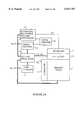
- FIG. 2Adepicts a flash memory according to an embodiment of the invention
- FIG. 2Bdepicts a flash memory according to an embodiment of the invention
- FIGS. 3A-Cdepict wordline voltages applied according to an embodiment of the invention
- FIGS. 4A-Cdepict wordline voltages applied according to an embodiment of the invention that employs an automatically adjusting voltage
- FIGS. 5A-Cdepict selected wordline voltages and selected sourceline voltages applied according to embodiments of the invention.
- FIG. 6Adepicts a wordline driver according to the prior art
- FIG. 6Bdepicts a wordline driver according to an embodiment of the invention
- FIG. 7depicts a wordline voltage applied according to the prior art
- FIGS. 8A-Cdepict wordline voltages applied according to an embodiment of the invention.
- FIGS. 9A-Cdepict wordline voltages applied according to an embodiment of the invention that employs a automatically adjusting voltage
- FIG. 10Adepicts a wordline driver according to the prior art.
- FIG. 10Bdepicts a wordline driver according to an embodiment of the invention.
- the inventioncan be used in any flash memory such as those including stacked-gate Flash cells, split-gate Flash cells, EEPROM, EPROM, BN+ cells, P-channel cells, or other types of flash cells.
- the inventioncan be also used in any memory array, including NOR-plane, NAND-plane, AND-plane, DINOR, dual-string NOR, or other types of memory arrays. All electrical parameters are given by example and can be modified with good results.
- the flash memoryincludes a memory array 11 that has a plurality of wordlines, bitlines and at least one sourceline.
- the memory array 11is constructed similarly to a conventional NOR-plane array.
- An X-decoder 12is coupled to the wordlines of array 11 and serves to apply operational voltages to selected and deselected wordlines.
- a Y-decoder 13is coupled to the bitlines of array 11 and serves to pass selected bitlines to a sense amplifier 14.
- the sourcelineis controlled by the Y-decoder (e.g. the sourceline decoder is within the Y-decoder), but could also be controlled by the X-decoder or by a separate sourceline decoder if desired.
- a voltage pump circuit 15is coupled to a voltage regulator 16 for supplying a variety of voltages to the memory.
- Voltage pump circuitsare known in the art and example is given by way of reference to U.S. Pat. Nos. 4,679,134 and 4,812,961. Additional type pumps that can be incorporated in the invention are described in U.S. Ser. No. 08/744,200 filed on Nov. 5, 1996; U.S. Ser. No. 08/772,232 filed on Dec. 23, 1996.
- the incorporation of a pump generator with the exemplary embodimentsexpands the operational voltages in order to facilitate improved yield and operation of the memory.
- the voltage pump generatorcreates the needed voltage and provides it to the decoder circuits to accomplish the necessary function.
- an automatically adjustable voltage controller 17is included in the flash memory.
- a timing controller 18is included in the flash memory.
- a state machine 19is configured to deliver predetermined voltages to the decoder circuits 12, 13 and array 11 as needed to perform a desired procedure. The function of these circuits is discussed in greater detail below.
- High speed erasingis an important improvement in flash memory technology. It is relevant to note that by decreasing the voltage applied to a tunnel oxide (more negative) the electrical field is increased.
- the inventiontherefore, significantly decreases the selected wordline voltage to very low voltages to speed the erase procedure.
- the best way to avoid device breakdown when further increasing or decreasing the voltage on selected wordlines beyond the specified BVDSSis to also increase or decrease the voltage on deselected wordlines. See, for example, FIG. 6B (described in detail below) where the two power inputs on lines 72a and 72b are connected to the wordlines 73a and 73b respectively. These two power inputs are connected to the source of M20a and M21a or M20b and M21b as indicated in FIG. 6B. Therefore, reducing the voltage across the source nodes of M20a and M21a is equivalent to reducing the voltage difference between selected wordlines and deselected wordlines.
- the inventionprovides a technique to lower both the selected wordline voltage Vg(sel) and the deselected wordline voltage Vg(desel) in order to maintain the differential voltage Vg(diff) below the breakdown voltage.
- the inventionprovides high erase speed while protecting the integrity of the wordline driver circuit.
- the lower selected voltage Vg(sel)also quickens the erase times for low threshold voltages such as from 2 V to 1 V.
- the lower erase-state Vtmeans lower read voltage can be realized. Hence, the flash memory power consumption can also be significantly reduced.
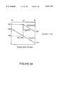
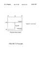
- FIG. 3Adepicts exemplary voltages applied to flash memory wordlines according to an embodiment of the invention.
- the applied sourceline voltageis typically positive, on the order of +5 V, and the bitline is disconnected and allowed to float.
- the voltage for the selected wordline Vg(sel)is ramped in region A-A' from an initial voltage -MV to a voltage -NV. This voltage is delivered to the array 11 via the X-decoder 12.
- the voltage ramp functionis performed by the timing control 18 and state machine 19.
- Vg(desel)is decreased one step Vg(desel)- ⁇ Vg, and then Vg(sel)- ⁇ Vg where ⁇ Vg is approximately 0.2 V.
- the deselected wordline voltageis stepped before the selected wordline. This order is beneficial to insure that the voltage difference remains below BVDSS.
- the erase and verificationis repeated again. This process iterates until Vg(sel) reaches -HV and Vg(desel) reaches -QV. If the erase verification still fails, then the part is considered to be defective.
- One reason to increase the voltage of Vg(desel) or Vg(sel)is to speed up the slowest erase cells or the high hole trapping cells.
- the voltage for the deselected wordlines Vg(desel)is also ramped from an initial voltage of 0 V to a voltage of -QV. This voltage is also delivered to the array 11 via the X-decoder 12, and the voltage ramp function is performed by the timing control 18 and state machine 19. From point A'-B, Vg(sel) is further ramped from the voltage -NV to the lower negative voltage -HV and Vg(desel) is ramped to the negative voltage -QV.
- Vg(desel)decreases one step first and then Vg(sel) follows the same voltage step to insure that the voltage difference between Vg(sel) and Vg(desel) remains less than BVDSS.
- Thisserves the two goals of reducing the initial voltage difference between Vg(sel) and Vs (source voltage) in order to avoid hole trapping in the oxide, and of permitting the Vg(sel) voltage to be lowered to -HV while keeping Vg(diff) below the breakdown voltage (BVDSS).
- the inventionperforms two functions in order to quicken the erase time.
- the inventioncan drive Vg(sel) to a highly negative voltage such as -12 V, -14 V, -16 V, -18 V, -20 V or more. This causes a large voltage differential between the gates and sources of the selected flash transistors thereby creating a strong electrical field that quickens the erase.
- the inventionlowers the voltage on the deselected wordlines Vg(desel) to -QV in order to reduce the possibility of a device breakdown in the X-decoder 12.
- There are two general techniques for providing the erase procedurethe first is time based and the second is threshold voltage based.
- the flash transistorsare always cycled through the same erase procedure. This procedure is a function of time.
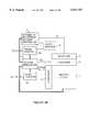
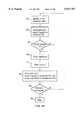
- FIG. 3Bis a flowchart showing the steps performed by the flash memory in order to apply the selected voltages to the wordlines.
- the proceduredetermines whether the voltage Vg(sel) has reached -NV. If not, step 34 is performed to stepwise reduce the Vg(sel) voltage one increment, for example 0.2 V. Then, step 30 is performed again to apply the reduced Vg(sel) voltage to the selected wordline.
- step 36stepwise reduces the Vg(desel) voltage one increment and step 37 stepwise reduces the Vg(sel) voltage one increment.
- Step 38then applies the Vg(sel) voltage to the selected wordline and the Vg(desel) voltage to the deselected wordline.
- Step 40determines whether the erase procedure is complete. If not, the procedure is returned to step 36 to further stepwise reduce the Vg(sel) voltage and Vg(desel) voltage.
- Step 36will stop reducing the Vg(sel) voltage and Vg(desel) voltage once Vg(sel) reaches -HV and Vg(desel) reaches -QV. At that point, step 36 maintains the voltages at those settings and passed the processing to step 38 until step 40 determines that the erasure is complete. Once step 40 determines that the erasure is complete, step 42 ends the erase procedure.
- FIG. 3Cdepicts an alternate aspect for applying Vg(desel) to the deselected wordlines.
- a large step in the deselected wordline voltage Vg(desel)is taken to -QV when Vg(sel) reaches -NV.
- -QVis about 2 V higher than -NV to insure proper operation of the X-decoder, since 2 V is about the sum of the PMOS Vtp and NMOS Vtn for safety inverter operation.
- the large step in Vg(desel)prevents Vg(diff) from exceeding the breakdown voltage similarly to that depicted in FIG. 3A.
- the erase proceduresenses the threshold of the flash transistors before erase and during erase verification.
- This techniqueuses the automatically adjustable voltage controller 17 shown in FIG. 2.
- the principal reason for the voltage based erase procedureis because threshold voltage Vt variations in flash transistors during manufacturing and over time cause the transistors to behave differently. For example, aged flash transistors typically take slightly longer to erase.
- the voltages for -MV, -NV, -QV and -HVare similar to those of the prior embodiment, but can also be modified if desired.
- the principal modification to this embodimentis that the flash transistor threshold voltage is iteratively sensed and so the voltages Vg(sel) and Vg(desel) are provided on demand based on the calculations performed by the controller 17.
- U.S. Ser. No. 08/779,765 filed Jan. 7, 1997describes a technique for sensing the threshold voltage of the flash transistors prior to and at selected times during the erase procedure.
- a benefit of this techniqueis that the maximum electrical field in all cells is kept constant during the entire erase procedure.
- Vg(sel)is a function of Vt, as shown in FIGS. 4A-B.
- the maximum erased cell's Vtis checked periodically, and then the bias condition is updated in accordance with the cell's Vt.
- This approachprovides an optimal control of the erasing operation, suppressing the spread of the cell's Vt distribution, and is accommodating to technology and process variations.
- FIG. 4Bis a flowchart showing the steps performed by the flash memory in order to perform the voltage based erasure.
- the selected cells' maximum threshold voltageis verified periodically, and then changing voltages are applied in accordance with the changing of the threshold voltage.
- the proceduresenses the maximum threshold voltage (Vt) of the flash transistors to be erased. This is performed by stepwise increasing (or decreasing) the wordline voltage until the cells' channels are turned on (or off).
- the sense amplifier 14senses the current and outputs a signal VT to the automatically adjusting voltage controller 17. In the case where multiple wordlines are selected, the sensing procedure is applied for all the selected wordlines.
- the automatically adjustable voltage controller 17calculates the target voltage to be applied to the selected wordline or wordlines Vg(sel) in order to efficiently erase the cells. In some cases Vg(sel) will begin at -MV, and in other cases Vg(sel) will be set below -MV.
- the target voltageis then communicated to the voltage regulator 16.
- the regulatorcontrols the output of the pump circuit 15 to generate the target voltages.
- the gate voltage Vg, drain voltage Vd and source voltage Vsare directly fed back from the selected cells to be compared to the target voltages.
- the automatically adjusting voltage controller 17is controls be the state machine 19.
- step 54the procedure determines whether the voltage Vg(sel) has reached -NV. If not, step 50 is again performed to calculate the Vg(sel) voltage and step 52 applies that voltage. If step 54 determines that Vg(sel) has reached -NV, then step 56 stepwise reduces the Vg(desel) voltage one increment and step 57 stepwise reduces the Vg(sel) voltage one increment. Step 58 then calculates and applies the Vg(desel) voltage to the deselected wordlines and the Vg(sel) voltage to the selected wordline or wordlines similar to that described in step 50. Step 60 determines whether the erase procedure is complete.
- step 56If not, the procedure is returned to step 56 to further stepwise reduce the Vg(sel) voltage and Vg(desel) voltage.
- Vg(sel) reaches -HV and Vg(desel) reaches -MV step 56maintains the voltages at those settings and passes the processing to step 58 until step 60 determines that the erasure is complete.
- step 62ends the erase procedure.
- FIG. 4Cdepicts an alternate aspect for applying Vg(desel) to the deselected wordlines.
- a large step in the deselected wordline voltage Vg(desel)is taken to -QV when Vg(sel) reaches -NV.
- -QVis about 2 V higher than -NV to insure proper operation of the X-decoder, since 2 V is about the sum of the PMOS Vtp and NMOS Vtn for safety inverter operation.
- the large step in Vg(desel)prevents Vg(diff) from exceeding the breakdown voltage similarly to that depicted in FIG. 4A.
- a further technique for increasing the erase speedincludes increasing the selected sourceline voltage to increase the maximum electric field in the flash transistors selected for erasure.
- a structure that provides control over the sourceline to selected flash transistorsis described in U.S. Ser. No. 08/872,475 filed Jun. 5, 1997. Such a structure can be controlled simultaneously with the X-decoder to apply operational voltages to the selected wordlines and selected sourcelines.
- the inventionapplies a sourceline voltage greater than the conventional voltage of 5 V. Unlike wordline voltage increases that gain only about 50% of the electrical field increase per volt increase, a sourceline voltage increase yields a 100% increase in the tunnel field per volt increase, thus increasing the erase current and speed by ten fold increase per volt increase.
- the maximum allowed sourceline voltageis limited by the BVDSS of the sourceline decoder. This sourceline voltage is about 10 V for a typical flash memory. Although a sourceline voltage increase quickens the erase procedure, a drawback is a resultant exponential increase in the substrate current between the P-N junction of the N+ source node and P substrate.
- the erase sizeis typically a block of 64K or 128K bytes. Conventional memories do not have a technique for providing sourceline voltage to a limited number of cells. Since the erase size is relatively large, a sourceline voltage (for EPROM-type flash) or bitline voltage (for EEPROM-type flash) is not recommended over +5 V when the wordline is coupled to -10 V.
- U.S. Ser. No. 08/872,475 filed on Jun. 5, 1997describes a technique to provide sourceline voltage to a specific number of cells.
- This novel techniqueprovides a new array architecture that permits a small erase size and provides that the percentage of slow-erase-speed cells and trapping cells is low (most likely only a few bytes).
- increasing the sourceline or bitline voltage beyond +5 Vis a highly effective technique.
- FIG. 5Adepicts exemplary voltages applied to selected flash memory wordlines and sourcelines according to an embodiment of the invention.
- the voltage for the selected wordline Vg(sel)is ramped in region A-A' from an initial voltage -MV to a voltage -NV.
- the voltage for the selected sourceline V(SL)is then ramped in the region A'-B from an initial voltage of +SV to a voltage +TV. This voltage is delivered to the array 11 via the X-decoder 12 or Y-decoder 13.
- Vg(sel)is further ramped in the region B-B' from voltage -NV to voltage -HV.
- the voltage ramp function for V(SL) and Vg(sel)is performed by the timing control 18 and state machine 19.
- FIG. 5Bdepicts an alternate aspect for applying V(SL) to the selected sourceline.
- V(SL)instead of applying a stepwise increasing voltage as in FIG. 5A, larger steps in the selected sourceline voltage V(SL) are taken to increase the voltage.
- V(SL)is increased from +SV to +PV.
- V(SL)is increased from +PV to +TV.
- +SV5 V
- +PV6 V
- FIG. 5Cdepicts another alternate aspect for applying V(SL) to the selected sourceline.
- V(SL)is stepwise increased from +SV to +PV.
- V(SL)is stepwise increased from +PV to +TV.
- +SV5 V
- +PV6 V
- oxide degradation occurring in conventional erasing procedureshas been observed to significantly reduce flash memory endurance. After many erase/program cycles, erasing efficiency is decreased due to the oxide degradation. As a result, it takes longer to erase aged cells than it does to erase new cells. In conventional flash memories, if the erase time takes longer than the specification allows, the erase will fail. Because conventional memories have predetermined fixed bias conditions, there is no way to change the condition after the cell's erasing efficiency is decreased. This problem has hindered the endurance of the prior art and limits the erase/program cycles in conventional flash memories to approximately 1M cycles.
- the gated breakdown conditionis that, low voltage at drain, and high voltage at all the other three electrodes, gate, source and bulk. Similarly if all the Vdg, Vds and Vdb exceed a specific voltage, the junction breakdown occurs.
- FIG. 6Adepicts a wordline driver according to the prior art.
- the gate of the selected cell M10ais applied with -HV from transistor M21a of the WL driver 70.
- the gate of the de-selected cell M10bis applied with 0 V from transistor M20b of the WL driver 70.
- the gate, source, drain and bulk of transistor M20ais 0 V, 0 V, -HV and 0 V, respectively.
- the transistoris turned off and is below a known "gated junction breakdown," in which, if the drain-bulk voltage difference is higher than BVDSS (approximately +/-10 V) the drain-bulk junction will breakdown and cause large current leakage to the bulk until the voltage difference is reduced. This phenomena constrains the voltage of the Vg(sel).
- transistor M21bis off and is also under the same constraints.
- FIG. 6Bdepicts a wordline driver according to an embodiment of the invention.
- -MVrather than 0 V
- the transistor M20ais relaxed from the junction breakdown structure because the bulk is -MV now and the drain-bulk voltage difference is reduced. Therefore, the drain of the transistor can be lowered to -(HV+MV) and still keep the same drain-bulk voltage difference below BVDSS. As a result, more negative gate voltage is available for selected cells to increase the erasing speed.
- the de-selected cell M10breceives gate voltage -MV, it is not erased. Because the source of the cell is 0 V, not +MV, the electrical field is not high enough to create a tunneling current and erase the cell.
- Vtinitial threshold voltage
- the first conventional artuses a constant selected wordline voltage Vg(sel) at -10 V.
- Vg(sel)As the cell's Vt decreases, the tunneling electrical field decreases, which causes the erasing time to increase at an approximately exponential rate. This results in fast erasing in the beginning but tremendously slow erasing when the cell's Vt becomes low. Experiments have shown a drawback of the fast erasing in the beginning that causes oxide degradation and significantly reduces the cell endurance.
- the second conventional artuses a stepwisely decreased Vg(sel) from about -6 V to -10 V (e.g. U.S. Pat. No. 5,485,423).
- Vg(sel)By decreasing Vg(sel) along the decreasing of cell's Vt, the tunneling electrical field is kept approximately constant and the starting portion of the erasing time is linear. The high field in the beginning is avoided and the oxide degradation is improved.
- Vg(sel)reaches the maximum negative value of -10 V, and it cannot decrease with the cell's Vt any more, the erasing time becomes exponential. As a result, this technique takes as long as the first conventional art to erase the cell to a low Vt in the 3 to 1 volt range.
- the inventionprovides that the Vg(sel) can continue to be reduced, unlike the conventional art.
- the Vg(sel)can be further decreased along the decreasing of the cell's Vt since a negative voltage is also applied to the deselected wordlines Vg(desel). Therefore, for the selected cells, the tunneling electrical field is kept high and constant and a linear erasing time is obtained for the entire erase procedure. This technique significantly reduces the erasing time and avoids oxide degradation.
- the methods to stepwise decrease Vg(sel) for the second conventional art and the inventionare different.
- the decreasing of Vg(sel)is purely a function of time and there is no corresponding decrease of Vg(desel).
- the decreasing of Vg(sel)is a function of cell's Vt and the number of erasing pulses. Due to variation of the cell's characteristic, the erasing speed of each cell is different. Many cells are erased simultaneously. However, the conventional art does not take care of the variation in erasing speed of the cells.
- the erasing time of a fast cellcan be one hundredth of that of a slow cell. It takes 10 ms to erase a fast cell from 4 V to 3 V, it may take 1 sec to erase a slow cell.
- the inventiondetects the slowest cells' Vt, and adjusts Vg(sel) according to the Vt. After a pre-determined number of pulses, if the cell's Vt is not lowered to a pre-determined value, the next Vg(sel) is applied. For example, if the slow cell can not be erased from 4 V to 3 V with ten pulses, which equals 100 ms, Vg(sel) is changed from -10 V to -12 V immediately. This increases the erasing speed by approximately 10 times.
- Vg(sel)is decreased to -14 V, which increases the erasing speed by approximately 100 times of that of -10 V, thus the slow cell can be erased within ten pulses, equal to 100 ms.
- the total erasing time for the slow cellis 300 ms, which is much faster than the conventional art.
- FIG. 7depicts a wordline voltage applied according to the prior art.
- a fixed voltage of this typeis similar to that described with reference to FIG. 1A.
- FIGS. 8A-Cdepict wordline voltages applied according to an embodiment of the invention that employs a time based program procedure similar to that described with reference to FIGS. 3A-C.
- FIGS. 9A-Cdepict wordline voltages applied according to an embodiment of the invention that employs a automatically adjusting program procedure similar to that described with reference to FIGS. 4A-C.
- the voltageis controlled by controller 17.
- FIG. 10Adepicts a wordline driver according to conventional art, similar to FIG. 6A.
- the voltage applied to the selected wordlinesis similarly limited because the voltage difference between the drain-bulk junction is limited to BVDSS. This phenomena constrains the voltage of the Vg(sel).
- FIG. 10Bdepicts a wordline driver according to an embodiment of the invention similar to FIG. 6B.
- +MVrather than 0 V
- the transistor M20ais relaxed from the junction breakdown structure, because the bulk is +MV now and the drain-bulk voltage difference is reduced. Therefore, the drain of the transistor can be raised to +(HV+MV) and still keep the same drain-bulk voltage difference below BVDSS.
- This gate voltage increase methodis mainly targeted to erase the EEPROM-type flash cells that defines the erase by application of a positive gate voltage as opposed to EPROM-type flash cells that defines the erase by application of a negative gate voltage.
- Both of these embodimentsprovide a program function that improves program speed and reduces the Vg(diff) on the wordline drivers.
- a voltage pump circuit 15is coupled to a voltage regulator 16 for supplying a variety of voltages to the memory.
- Voltage pump circuitsare known in the art and example is given by way of reference to U.S. Pat. Nos. 4,679,134 and 4,812,961. Additional types of pumps that can be incorporated in the invention are described in U.S. Ser. No. 08/744,200 filed on Nov. 5, 1997; U.S. Ser. No. 08/772,232 filed on Dec. 23, 1996 (Atty Docket No. A-64099/TOH/MAK); and U.S. Ser. No. 08/814,913 filed Mar. 11, 1997.
- the incorporation of a pump generator with the exemplary embodimentsexpands the operational voltages in order to facilitate improved yield and operation of the memory.
- the voltage pump generatorcreates the needed voltage and provides it to the decoder circuits to accomplish the necessary function.
- Advantages of the inventioninclude a fast erasing procedure due to the increased voltage differential applied between the gate and source of flash transistors selected to be erased. Moreover, since the deselected wordlines are also ramped to either a negative or positive voltage along with the selected wordline voltage raised to a greater negative or positive voltage, stress is reduced on the wordline drivers, thereby increasing the longevity of the flash memory.
Landscapes
- Engineering & Computer Science (AREA)
- Computer Hardware Design (AREA)
- Power Engineering (AREA)
- Microelectronics & Electronic Packaging (AREA)
- Physics & Mathematics (AREA)
- Nonlinear Science (AREA)
- Electromagnetism (AREA)
- General Physics & Mathematics (AREA)
- Radar, Positioning & Navigation (AREA)
- Automation & Control Theory (AREA)
- Read Only Memory (AREA)
Abstract
Description
______________________________________Vg (sel) Vt Time______________________________________(a) First Conventional Art-10 V 6 V to 5 V 100 us (exponential) (most severe oxide degrade)-10V 5 V to 4 V 1 ms (exponential) (severe oxide degrade)-10 V 4 V to 3 V 10 ms (exponential) (negligible oxide degrade)-10 V 3 V to 2 V 100 ms (exponential) (negligible oxide degrade)-10 V 2 V to 1 V 1 s (exponential) (negligible oxide degrade)Total time: approximately 1.1 sec.(b) Second Conventional Art -6 V 6 V to 5 V 10 ms (linear) (negligible oxide degrade) -8V 5 V to 4 V 10 ms (linear) (negligible oxide degrade)-10 V 4 V to 3 V 10 ms (linear) (negligible oxide degrade)-10 V 3 V to 2 V 100 ms (exponential) (negligible oxide degrade)-10 V 2 V to 1 V 1 s (exponential) (negligible oxide degrade)Total time: approximately 1.1 sec.(c) The Invention -6 V 6 V to 5 V 10 ms (linear) (negligible oxide degrade) -8V 5 V to 4 V 10 ms (linear) (negligible oxide degrade)-10 V 4 V to 3 V 10 ms (linear) (negligible oxide degrade)-12 V* 3 V to 2 V 10 ms (linear) (negligible oxide degrade)-14 V* 2 V to 1 V 10 ms (linear) (negligible oxide degrade)Total time: approximately 0.05 sec.______________________________________ *In this voltage range, the Xdecoder driver operates at a greater BVDSS with respect to a negative voltage as opposed to the conventional BVDSS voltage of -10 V with respect to ground.
Claims (40)
Priority Applications (2)
| Application Number | Priority Date | Filing Date | Title |
|---|---|---|---|
| US08/882,558US5917757A (en) | 1996-08-01 | 1997-06-25 | Flash memory with high speed erasing structure using thin oxide semiconductor devices |
| US08/915,344US5914896A (en) | 1996-08-01 | 1997-08-22 | Flash memory with high speed erasing structure using thin oxide and thick oxide semiconductor devices |
Applications Claiming Priority (8)
| Application Number | Priority Date | Filing Date | Title |
|---|---|---|---|
| US08/691,281US5796657A (en) | 1996-03-29 | 1996-08-01 | Flash memory with flexible erasing size from multi-byte to multi-block |
| US74420096A | 1996-11-05 | 1996-11-05 | |
| US77223296A | 1996-12-23 | 1996-12-23 | |
| US77976597A | 1997-01-07 | 1997-01-07 | |
| US08/814,913US5859571A (en) | 1997-03-11 | 1997-03-11 | Frequency trimmable oscillator and frequency multiplier |
| US08/823,571US6381670B1 (en) | 1997-01-07 | 1997-03-25 | Flash memory array having maximum and minimum threshold voltage detection for eliminating over-erasure problem and enhancing write operation |
| US08/872,475US5777924A (en) | 1997-06-05 | 1997-06-05 | Flash memory array and decoding architecture |
| US08/882,558US5917757A (en) | 1996-08-01 | 1997-06-25 | Flash memory with high speed erasing structure using thin oxide semiconductor devices |
Related Parent Applications (7)
| Application Number | Title | Priority Date | Filing Date |
|---|---|---|---|
| US08/691,281Continuation-In-PartUS5796657A (en) | 1996-03-29 | 1996-08-01 | Flash memory with flexible erasing size from multi-byte to multi-block |
| US74420096AContinuation-In-Part | 1996-08-01 | 1996-11-05 | |
| US77223296AContinuation-In-Part | 1996-08-01 | 1996-12-23 | |
| US77976597AContinuation-In-Part | 1996-03-29 | 1997-01-07 | |
| US08/814,913Continuation-In-PartUS5859571A (en) | 1996-08-01 | 1997-03-11 | Frequency trimmable oscillator and frequency multiplier |
| US08/823,571Continuation-In-PartUS6381670B1 (en) | 1996-08-01 | 1997-03-25 | Flash memory array having maximum and minimum threshold voltage detection for eliminating over-erasure problem and enhancing write operation |
| US08/872,475Continuation-In-PartUS5777924A (en) | 1996-03-29 | 1997-06-05 | Flash memory array and decoding architecture |
Related Child Applications (1)
| Application Number | Title | Priority Date | Filing Date |
|---|---|---|---|
| US08/915,344Continuation-In-PartUS5914896A (en) | 1996-08-01 | 1997-08-22 | Flash memory with high speed erasing structure using thin oxide and thick oxide semiconductor devices |
Publications (1)
| Publication Number | Publication Date |
|---|---|
| US5917757Atrue US5917757A (en) | 1999-06-29 |
Family
ID=27569885
Family Applications (1)
| Application Number | Title | Priority Date | Filing Date |
|---|---|---|---|
| US08/882,558Expired - LifetimeUS5917757A (en) | 1996-08-01 | 1997-06-25 | Flash memory with high speed erasing structure using thin oxide semiconductor devices |
Country Status (1)
| Country | Link |
|---|---|
| US (1) | US5917757A (en) |
Cited By (24)
| Publication number | Priority date | Publication date | Assignee | Title |
|---|---|---|---|---|
| US6016275A (en)* | 1998-03-13 | 2000-01-18 | Lg Semicon Co., Ltd. | Flash memory wear leveling system and method |
| US6160740A (en)* | 1999-12-17 | 2000-12-12 | Advanced Micro Devices, Inc. | Method to provide a reduced constant E-field during erase of EEPROMs for reliability improvement |
| WO2001063618A1 (en)* | 2000-02-25 | 2001-08-30 | Advanced Micro Devices, Inc. | Wordline driver for flash memory read mode |
| US6314027B1 (en)* | 1999-07-28 | 2001-11-06 | Samsung Electronics Co., Ltd. | Flash memory device capable of preventing an over-erasure of flash memory cells and erase method thereof |
| US6584034B1 (en)* | 2001-04-23 | 2003-06-24 | Aplus Flash Technology Inc. | Flash memory array structure suitable for multiple simultaneous operations |
| US20030122216A1 (en)* | 2001-12-28 | 2003-07-03 | Rabadam Eleanor P. | Memory device packaging including stacked passive devices and method for making the same |
| EP1569242A1 (en)* | 2004-02-27 | 2005-08-31 | STMicroelectronics S.r.l. | Electrically word-erasable non-volatile memory-device, and biasing method thereof |
| US20050232022A1 (en)* | 1999-07-28 | 2005-10-20 | Samsung Electronics Co., Ltd. | Flash memory device capable of preventing an over-erase of flash memory cells and erase method thereof |
| US20050248990A1 (en)* | 2004-05-07 | 2005-11-10 | Micron Technology, Inc. | Flash memory device with improved programming performance |
| US20060002167A1 (en)* | 2004-06-30 | 2006-01-05 | Micron Technology, Inc. | Minimizing adjacent wordline disturb in a memory device |
| US20060279999A1 (en)* | 2005-06-13 | 2006-12-14 | Samsung Electronics Co., Ltd. | Methods of Erasing Flash Memory Devices by Applying Wordline Bias Voltages Having Multiple Levels and Related Flash Memory Devices |
| US20070183219A1 (en)* | 1999-07-28 | 2007-08-09 | Samsung Electronics Co., Ltd. | Flash memory device capable of preventing an overerase of flash memory cells and erase method thereof |
| US20080049494A1 (en)* | 2006-08-22 | 2008-02-28 | Micron Technology, Inc. | Reducing effects of program disturb in a memory device |
| US20080123425A1 (en)* | 2006-11-02 | 2008-05-29 | Lutze Jeffrey W | Reducing program disturb in non-volatile memory using multiple boosting modes |
| US20080123426A1 (en)* | 2006-11-02 | 2008-05-29 | Lutze Jeffrey W | Non-volatile memory using multiple boosting modes for reduced program disturb |
| WO2008057927A3 (en)* | 2006-11-02 | 2008-07-24 | Sandisk Corp | Reducing program disturb in non-volatile memory using multiple boosting modes |
| US20080291730A1 (en)* | 2006-02-22 | 2008-11-27 | Micron Technology, Inc. | Reducing effects of program disturb in a memory device |
| US20090011560A1 (en)* | 2006-04-12 | 2009-01-08 | Seiichi Aritome | Multiple select gate architecture with select gates of different lengths |
| US20090273979A1 (en)* | 2006-03-28 | 2009-11-05 | Micron Technology, Inc. | Programming method to reduce word line to word line breakdown for nand flash |
| US7733705B2 (en) | 2008-03-13 | 2010-06-08 | Micron Technology, Inc. | Reduction of punch-through disturb during programming of a memory device |
| US8345485B2 (en) | 2011-02-09 | 2013-01-01 | Freescale Semiconductor, Inc. | Erase ramp pulse width control for non-volatile memory |
| US20140019675A1 (en)* | 2012-07-11 | 2014-01-16 | Eun Chu Oh | Nonvolatle memory device and memory system having the same, and related memory management, erase and programming methods |
| US20150146487A1 (en)* | 2013-11-22 | 2015-05-28 | SK Hynix Inc. | Non-volatile memory device and method for erasing the same |
| US9564236B2 (en)* | 2014-12-08 | 2017-02-07 | Winbond Electronics Corp. | NAND flash memory and reading method thereof |
Citations (13)
| Publication number | Priority date | Publication date | Assignee | Title |
|---|---|---|---|---|
| US4357685A (en)* | 1979-09-28 | 1982-11-02 | Sgs-Ates Componenti Elettronici S.P.A. | Method of programming an electrically alterable nonvolatile memory |
| US5485423A (en)* | 1994-10-11 | 1996-01-16 | Advanced Micro Devices, Inc. | Method for eliminating of cycling-induced electron trapping in the tunneling oxide of 5 volt only flash EEPROMS |
| US5532960A (en)* | 1993-08-31 | 1996-07-02 | Macronix International Co., Ltd. | Negative voltage generator for flash EPROM design |
| US5535158A (en)* | 1993-12-01 | 1996-07-09 | Nec Corporation | Non-volatile semiconductor memory device and method for erasure and production thereof |
| US5568419A (en)* | 1994-07-28 | 1996-10-22 | Kabushiki Kaisha Toshiba | Non-volatile semiconductor memory device and data erasing method therefor |
| US5574686A (en)* | 1993-01-27 | 1996-11-12 | Seiko Epson Corporation | Nonvolatile semiconductor storage system |
| US5587947A (en)* | 1994-03-03 | 1996-12-24 | Rohm Corporation | Low voltage one transistor flash EEPROM cell using Fowler-Nordheim programming and erase |
| US5600593A (en)* | 1994-12-06 | 1997-02-04 | National Semiconductor Corporation | Apparatus and method for reducing erased threshold voltage distribution in flash memory arrays |
| US5612913A (en)* | 1994-09-27 | 1997-03-18 | Sgs-Thomson Microelectronics, S.R.L. | Byte erasable EEPROM fully compatible with a single power supply flash-EPROM process |
| US5661683A (en)* | 1996-02-05 | 1997-08-26 | Integrated Silicon Solution Inc. | On-chip positive and negative high voltage wordline x-decoding for EPROM/FLASH |
| US5703807A (en)* | 1996-07-19 | 1997-12-30 | Texas Instruments Incorporated | EEPROM with enhanced reliability by selectable VPP for write and erase |
| US5712819A (en)* | 1988-06-08 | 1998-01-27 | Harari; Eliyahou | Flash EEPROM system with storage of sector characteristic information within the sector |
| US5721704A (en)* | 1996-08-23 | 1998-02-24 | Motorola, Inc. | Control gate driver circuit for a non-volatile memory and memory using same |
- 1997
- 1997-06-25USUS08/882,558patent/US5917757A/ennot_activeExpired - Lifetime
Patent Citations (13)
| Publication number | Priority date | Publication date | Assignee | Title |
|---|---|---|---|---|
| US4357685A (en)* | 1979-09-28 | 1982-11-02 | Sgs-Ates Componenti Elettronici S.P.A. | Method of programming an electrically alterable nonvolatile memory |
| US5712819A (en)* | 1988-06-08 | 1998-01-27 | Harari; Eliyahou | Flash EEPROM system with storage of sector characteristic information within the sector |
| US5574686A (en)* | 1993-01-27 | 1996-11-12 | Seiko Epson Corporation | Nonvolatile semiconductor storage system |
| US5532960A (en)* | 1993-08-31 | 1996-07-02 | Macronix International Co., Ltd. | Negative voltage generator for flash EPROM design |
| US5535158A (en)* | 1993-12-01 | 1996-07-09 | Nec Corporation | Non-volatile semiconductor memory device and method for erasure and production thereof |
| US5587947A (en)* | 1994-03-03 | 1996-12-24 | Rohm Corporation | Low voltage one transistor flash EEPROM cell using Fowler-Nordheim programming and erase |
| US5568419A (en)* | 1994-07-28 | 1996-10-22 | Kabushiki Kaisha Toshiba | Non-volatile semiconductor memory device and data erasing method therefor |
| US5612913A (en)* | 1994-09-27 | 1997-03-18 | Sgs-Thomson Microelectronics, S.R.L. | Byte erasable EEPROM fully compatible with a single power supply flash-EPROM process |
| US5485423A (en)* | 1994-10-11 | 1996-01-16 | Advanced Micro Devices, Inc. | Method for eliminating of cycling-induced electron trapping in the tunneling oxide of 5 volt only flash EEPROMS |
| US5600593A (en)* | 1994-12-06 | 1997-02-04 | National Semiconductor Corporation | Apparatus and method for reducing erased threshold voltage distribution in flash memory arrays |
| US5661683A (en)* | 1996-02-05 | 1997-08-26 | Integrated Silicon Solution Inc. | On-chip positive and negative high voltage wordline x-decoding for EPROM/FLASH |
| US5703807A (en)* | 1996-07-19 | 1997-12-30 | Texas Instruments Incorporated | EEPROM with enhanced reliability by selectable VPP for write and erase |
| US5721704A (en)* | 1996-08-23 | 1998-02-24 | Motorola, Inc. | Control gate driver circuit for a non-volatile memory and memory using same |
Cited By (67)
| Publication number | Priority date | Publication date | Assignee | Title |
|---|---|---|---|---|
| US6016275A (en)* | 1998-03-13 | 2000-01-18 | Lg Semicon Co., Ltd. | Flash memory wear leveling system and method |
| US7190624B2 (en) | 1999-07-28 | 2007-03-13 | Samsung Electronics Co., Ltd. | Flash memory device capable of preventing an over-erase of flash memory cells and erase method thereof |
| US7366020B2 (en) | 1999-07-28 | 2008-04-29 | Samsung Electronics Co., Ltd. | Flash memory device capable of preventing an overerase of flash memory cells and erase method thereof |
| US6314027B1 (en)* | 1999-07-28 | 2001-11-06 | Samsung Electronics Co., Ltd. | Flash memory device capable of preventing an over-erasure of flash memory cells and erase method thereof |
| US6577540B2 (en)* | 1999-07-28 | 2003-06-10 | Samsung Electronics Co., Ltd. | Flash memory device capable of preventing an over-erase of flash memory cells and erase method thereof |
| US20050232022A1 (en)* | 1999-07-28 | 2005-10-20 | Samsung Electronics Co., Ltd. | Flash memory device capable of preventing an over-erase of flash memory cells and erase method thereof |
| US20070183219A1 (en)* | 1999-07-28 | 2007-08-09 | Samsung Electronics Co., Ltd. | Flash memory device capable of preventing an overerase of flash memory cells and erase method thereof |
| US6160740A (en)* | 1999-12-17 | 2000-12-12 | Advanced Micro Devices, Inc. | Method to provide a reduced constant E-field during erase of EEPROMs for reliability improvement |
| US6400638B1 (en) | 2000-02-25 | 2002-06-04 | Advanced Micro Devices, Inc. | Wordline driver for flash memory read mode |
| WO2001063618A1 (en)* | 2000-02-25 | 2001-08-30 | Advanced Micro Devices, Inc. | Wordline driver for flash memory read mode |
| US20030206456A1 (en)* | 2001-04-23 | 2003-11-06 | Aplus Flash Technology, Inc. | Novel flash memory array structure suitable for multiple simultaneous operations |
| US6788611B2 (en)* | 2001-04-23 | 2004-09-07 | Aplus Flash Technology, Inc. | Flash memory array structure suitable for multiple simultaneous operations |
| US6788612B2 (en)* | 2001-04-23 | 2004-09-07 | Aplus Flash Technology, Inc. | Flash memory array structure suitable for multiple simultaneous operations |
| US20030206455A1 (en)* | 2001-04-23 | 2003-11-06 | Aplus Flash Technology, Inc. | Novel flash memory array structure suitable for multiple simultaneous operations |
| US6584034B1 (en)* | 2001-04-23 | 2003-06-24 | Aplus Flash Technology Inc. | Flash memory array structure suitable for multiple simultaneous operations |
| US20030122216A1 (en)* | 2001-12-28 | 2003-07-03 | Rabadam Eleanor P. | Memory device packaging including stacked passive devices and method for making the same |
| EP1569242A1 (en)* | 2004-02-27 | 2005-08-31 | STMicroelectronics S.r.l. | Electrically word-erasable non-volatile memory-device, and biasing method thereof |
| US20050195654A1 (en)* | 2004-02-27 | 2005-09-08 | Stmicroelectronics S.R.I. | Electrically word-erasable non-volatile memory device, and biasing method thereof |
| US7130219B2 (en) | 2004-02-27 | 2006-10-31 | Stmicroelectronics S.R.L. | Electrically word-erasable non-volatile memory device, and biasing method thereof |
| US20050248990A1 (en)* | 2004-05-07 | 2005-11-10 | Micron Technology, Inc. | Flash memory device with improved programming performance |
| US7038945B2 (en) | 2004-05-07 | 2006-05-02 | Micron Technology, Inc. | Flash memory device with improved programming performance |
| US20060146611A1 (en)* | 2004-05-07 | 2006-07-06 | Micron Technology, Inc. | Flash memory device with improved programming performance |
| US7280403B2 (en) | 2004-05-07 | 2007-10-09 | Micron Technology, Inc. | Flash memory device with improved programming performance |
| US7120055B2 (en) | 2004-05-07 | 2006-10-10 | Micron Technology, Inc. | Flash memory device with improved programming performance |
| US20070014158A1 (en)* | 2004-05-07 | 2007-01-18 | Micron Technology, Inc. | Flash memory device with improved programming performance |
| US20060002167A1 (en)* | 2004-06-30 | 2006-01-05 | Micron Technology, Inc. | Minimizing adjacent wordline disturb in a memory device |
| US7212435B2 (en) | 2004-06-30 | 2007-05-01 | Micron Technology, Inc. | Minimizing adjacent wordline disturb in a memory device |
| US20060198221A1 (en)* | 2004-06-30 | 2006-09-07 | Micron Technology, Inc. | Minimizing adjacent wordline disturb in a memory device |
| US7257024B2 (en) | 2004-06-30 | 2007-08-14 | Micron Technology, Inc. | Minimizing adjacent wordline disturb in a memory device |
| US7272039B2 (en) | 2004-06-30 | 2007-09-18 | Micron Technology, Inc. | Minimizing adjacent wordline disturb in a memory device |
| US20060198222A1 (en)* | 2004-06-30 | 2006-09-07 | Micron Technology, Inc. | Minimizing adjacent wordline disturb in a memory device |
| WO2006012292A1 (en)* | 2004-06-30 | 2006-02-02 | Micron Technology, Inc. | Minimizing adjacent wordline disturb in a memory device |
| US7397706B2 (en)* | 2005-06-13 | 2008-07-08 | Samsung Electronics Co., Ltd. | Methods of erasing flash memory devices by applying wordline bias voltages having multiple levels and related flash memory devices |
| US20060279999A1 (en)* | 2005-06-13 | 2006-12-14 | Samsung Electronics Co., Ltd. | Methods of Erasing Flash Memory Devices by Applying Wordline Bias Voltages Having Multiple Levels and Related Flash Memory Devices |
| US7715234B2 (en) | 2006-02-22 | 2010-05-11 | Micron Technology, Inc. | Reducing effects of program disturb in a memory device |
| US8023329B2 (en) | 2006-02-22 | 2011-09-20 | Micron Technology, Inc. | Reducing effects of program disturb in a memory device |
| US20080291730A1 (en)* | 2006-02-22 | 2008-11-27 | Micron Technology, Inc. | Reducing effects of program disturb in a memory device |
| US20100202210A1 (en)* | 2006-02-22 | 2010-08-12 | Micron Technology, Inc. | Reducing effects of program disturb in a memory device |
| US20090273979A1 (en)* | 2006-03-28 | 2009-11-05 | Micron Technology, Inc. | Programming method to reduce word line to word line breakdown for nand flash |
| US7924619B2 (en) | 2006-03-28 | 2011-04-12 | Micron Technology, Inc. | Programming method to reduce word line to word line breakdown for NAND flash |
| US20090011560A1 (en)* | 2006-04-12 | 2009-01-08 | Seiichi Aritome | Multiple select gate architecture with select gates of different lengths |
| US7729171B2 (en) | 2006-04-12 | 2010-06-01 | Micron Technology, Inc. | Multiple select gate architecture with select gates of different lengths |
| US7471565B2 (en) | 2006-08-22 | 2008-12-30 | Micron Technology, Inc. | Reducing effects of program disturb in a memory device |
| US7898861B2 (en) | 2006-08-22 | 2011-03-01 | Micron Technology, Inc. | Reducing effects of program disturb in a memory device |
| US20090046507A1 (en)* | 2006-08-22 | 2009-02-19 | Micron Technology, Inc. | Reducing effects of program disturb in a memory device |
| US8159879B2 (en) | 2006-08-22 | 2012-04-17 | Micron Technology, Inc. | Reducing effects of program disturb in a memory device |
| US20080049494A1 (en)* | 2006-08-22 | 2008-02-28 | Micron Technology, Inc. | Reducing effects of program disturb in a memory device |
| US8325520B2 (en) | 2006-08-22 | 2012-12-04 | Micron Technology, Inc. | Reducing effects of program disturb in a memory device |
| KR101012133B1 (en) | 2006-11-02 | 2011-02-07 | 샌디스크 코포레이션 | How to reduce program disturb in nonvolatile memory using multiple boosting modes |
| US20080123425A1 (en)* | 2006-11-02 | 2008-05-29 | Lutze Jeffrey W | Reducing program disturb in non-volatile memory using multiple boosting modes |
| US7796430B2 (en) | 2006-11-02 | 2010-09-14 | Sandisk Corporation | Non-volatile memory using multiple boosting modes for reduced program disturb |
| US20080123426A1 (en)* | 2006-11-02 | 2008-05-29 | Lutze Jeffrey W | Non-volatile memory using multiple boosting modes for reduced program disturb |
| US20090010065A1 (en)* | 2006-11-02 | 2009-01-08 | Lutze Jeffrey W | Non-volatile memory using multiple boosting modes for reduced program disturb |
| US7468911B2 (en) | 2006-11-02 | 2008-12-23 | Sandisk Corporation | Non-volatile memory using multiple boosting modes for reduced program disturb |
| CN101589436B (en)* | 2006-11-02 | 2013-01-30 | 桑迪士克科技公司 | Reduce Program Disturbance Using Multiple Boost Modes in Nonvolatile Memory |
| US7440323B2 (en) | 2006-11-02 | 2008-10-21 | Sandisk Corporation | Reducing program disturb in non-volatile memory using multiple boosting modes |
| WO2008057927A3 (en)* | 2006-11-02 | 2008-07-24 | Sandisk Corp | Reducing program disturb in non-volatile memory using multiple boosting modes |
| US8164950B2 (en) | 2008-03-13 | 2012-04-24 | Micron Technology, Inc. | Reduction of punch-through disturb during programming of a memory device |
| US7733705B2 (en) | 2008-03-13 | 2010-06-08 | Micron Technology, Inc. | Reduction of punch-through disturb during programming of a memory device |
| US20110116311A1 (en)* | 2008-03-13 | 2011-05-19 | Micron Technology, Inc. | Reduction of punch-through disturb during programming of a memory device |
| US8345485B2 (en) | 2011-02-09 | 2013-01-01 | Freescale Semiconductor, Inc. | Erase ramp pulse width control for non-volatile memory |
| US20140019675A1 (en)* | 2012-07-11 | 2014-01-16 | Eun Chu Oh | Nonvolatle memory device and memory system having the same, and related memory management, erase and programming methods |
| US9390001B2 (en)* | 2012-07-11 | 2016-07-12 | Samsung Electronics Co., Ltd. | Nonvolatle memory device and memory system having the same, and related memory management, erase and programming methods |
| US9818485B2 (en) | 2012-07-11 | 2017-11-14 | Samsung Electronics Co., Ltd. | Nonvolatle memory device and memory system having the same, and related memory management, erase and programming methods |
| US20150146487A1 (en)* | 2013-11-22 | 2015-05-28 | SK Hynix Inc. | Non-volatile memory device and method for erasing the same |
| US9064584B2 (en)* | 2013-11-22 | 2015-06-23 | SK Hynix Inc. | Non-volatile memory device and method for erasing the same |
| US9564236B2 (en)* | 2014-12-08 | 2017-02-07 | Winbond Electronics Corp. | NAND flash memory and reading method thereof |
Similar Documents
| Publication | Publication Date | Title |
|---|---|---|
| US5917757A (en) | Flash memory with high speed erasing structure using thin oxide semiconductor devices | |
| KR100328359B1 (en) | A flash memory device capable of minimizing a substrate voltage bouncing and a program method thereof | |
| US5914896A (en) | Flash memory with high speed erasing structure using thin oxide and thick oxide semiconductor devices | |
| CN105185409B (en) | Memory architecture with two independently controlled voltage pumps | |
| US6031766A (en) | Method and circuit for substrate current induced hot e-injection (SCIHE) approach for VT convergence at low Vcc voltage | |
| US6469933B2 (en) | Flash memory device capable of preventing program disturb and method for programming the same | |
| JP3737525B2 (en) | Semiconductor memory device | |
| KR100290283B1 (en) | Nonvolatile semiconductor memory device and word line driving method thereof | |
| US7460411B2 (en) | Array source line (AVSS) controlled high voltage regulation for programming flash or EE array | |
| US20010012219A1 (en) | Voltage regulator circuit built in a semiconductor memory device | |
| US8289777B2 (en) | Semiconductor memory device | |
| JPH07122998B2 (en) | High voltage generation circuit for semiconductor memory device | |
| JP2007506207A (en) | Boost substrate for flash memory / tab programming | |
| CN101162609A (en) | Non-volatile memory devices and methods of programming the same | |
| US6483750B2 (en) | Flash EEPROM with on-chip erase source voltage generator | |
| US6735125B2 (en) | Nonvolatile semiconductor memory device and method of erasing the same | |
| US6281665B1 (en) | High speed internal voltage generator with reduced current draw | |
| US5901090A (en) | Method for erasing flash electrically erasable programmable read-only memory (EEPROM) | |
| US5920505A (en) | Negative word line voltage regulation circuit for electrically erasable semiconductor memory devices | |
| JP3914340B2 (en) | Flash memory device | |
| US5875130A (en) | Method for programming flash electrically erasable programmable read-only memory | |
| US5784319A (en) | Method for erasing an electrically programmable and erasable non-volatile memory cell | |
| KR20010044901A (en) | Nonvolatile semiconductor memory device which is capable of reducing read time | |
| US20080247237A1 (en) | Semiconductor memory device in which sense timing of sense amplifier can be controlled by constant current charge | |
| US6438041B1 (en) | Negative voltage regulation |
Legal Events
| Date | Code | Title | Description |
|---|---|---|---|
| AS | Assignment | Owner name:APLUS INTEGRATED CIRCUITS, INC., CALIFORNIA Free format text:ASSIGNMENT OF ASSIGNORS INTEREST;ASSIGNORS:LEE, PETER W.;HSU, FU-CHANG;TSAO, HSING-YA;REEL/FRAME:008939/0663 Effective date:19980120 | |
| AS | Assignment | Owner name:APLUS FLASH TECHNOLOGY, INC., CALIFORNIA Free format text:ASSIGNMENT OF ASSIGNORS INTEREST;ASSIGNOR:APLUS INTEGRATED CIRCUITS, INC.;REEL/FRAME:009038/0608 Effective date:19980302 | |
| STCF | Information on status: patent grant | Free format text:PATENTED CASE | |
| FPAY | Fee payment | Year of fee payment:4 | |
| REMI | Maintenance fee reminder mailed | ||
| FPAY | Fee payment | Year of fee payment:8 | |
| SULP | Surcharge for late payment | Year of fee payment:7 | |
| FEPP | Fee payment procedure | Free format text:PAT HOLDER NO LONGER CLAIMS SMALL ENTITY STATUS, ENTITY STATUS SET TO UNDISCOUNTED (ORIGINAL EVENT CODE: STOL); ENTITY STATUS OF PATENT OWNER: LARGE ENTITY | |
| FEPP | Fee payment procedure | Free format text:PAYOR NUMBER ASSIGNED (ORIGINAL EVENT CODE: ASPN); ENTITY STATUS OF PATENT OWNER: LARGE ENTITY | |
| AS | Assignment | Owner name:ABEDNEJA ASSETS AG L.L.C., DELAWARE Free format text:ASSIGNMENT OF ASSIGNORS INTEREST;ASSIGNOR:APLUS FLASH TECHNOLOGY, INC.;REEL/FRAME:022562/0920 Effective date:20090224 | |
| FPAY | Fee payment | Year of fee payment:12 | |
| FEPP | Fee payment procedure | Free format text:PAYER NUMBER DE-ASSIGNED (ORIGINAL EVENT CODE: RMPN); ENTITY STATUS OF PATENT OWNER: LARGE ENTITY Free format text:PAYOR NUMBER ASSIGNED (ORIGINAL EVENT CODE: ASPN); ENTITY STATUS OF PATENT OWNER: LARGE ENTITY | |
| AS | Assignment | Owner name:INTELLECTUAL VENTURES FUND 100 LLC, DELAWARE Free format text:ASSIGNMENT OF ASSIGNORS INTEREST;ASSIGNOR:ABEDNEJA ASSETS AG L.L.C.;REEL/FRAME:031841/0255 Effective date:20131219 | |
| AS | Assignment | Owner name:INTELLECTUAL VENTURES FUND 100 LLC, DELAWARE Free format text:SECURITY AGREEMENT;ASSIGNOR:SECURE AXCESS LLC;REEL/FRAME:032168/0279 Effective date:20131220 Owner name:INTELLECTUAL VENTURES HOLDING 47 LLC, DELAWARE Free format text:SECURITY AGREEMENT;ASSIGNOR:SECURE AXCESS LLC;REEL/FRAME:032168/0279 Effective date:20131220 | |
| AS | Assignment | Owner name:SECURE AXCESS LLC, TEXAS Free format text:ASSIGNMENT OF ASSIGNORS INTEREST;ASSIGNOR:INTELLECTUAL VENTURES FUND 100 LLC;REEL/FRAME:032342/0065 Effective date:20131230 |