US5917335A - Output voltage controlled impedance output buffer - Google Patents
Output voltage controlled impedance output bufferDownload PDFInfo
- Publication number
- US5917335A US5917335AUS08/837,782US83778297AUS5917335AUS 5917335 AUS5917335 AUS 5917335AUS 83778297 AUS83778297 AUS 83778297AUS 5917335 AUS5917335 AUS 5917335A
- Authority
- US
- United States
- Prior art keywords
- output
- voltage
- transistor
- circuit
- impedance
- Prior art date
- Legal status (The legal status is an assumption and is not a legal conclusion. Google has not performed a legal analysis and makes no representation as to the accuracy of the status listed.)
- Expired - Lifetime
Links
Images

Classifications
- H—ELECTRICITY
- H03—ELECTRONIC CIRCUITRY
- H03K—PULSE TECHNIQUE
- H03K19/00—Logic circuits, i.e. having at least two inputs acting on one output; Inverting circuits
- H03K19/003—Modifications for increasing the reliability for protection
- H03K19/00346—Modifications for eliminating interference or parasitic voltages or currents
- H03K19/00361—Modifications for eliminating interference or parasitic voltages or currents in field effect transistor circuits
- H—ELECTRICITY
- H03—ELECTRONIC CIRCUITRY
- H03K—PULSE TECHNIQUE
- H03K19/00—Logic circuits, i.e. having at least two inputs acting on one output; Inverting circuits
- H03K19/0005—Modifications of input or output impedance
- H—ELECTRICITY
- H03—ELECTRONIC CIRCUITRY
- H03K—PULSE TECHNIQUE
- H03K19/00—Logic circuits, i.e. having at least two inputs acting on one output; Inverting circuits
- H03K19/01—Modifications for accelerating switching
- H03K19/017—Modifications for accelerating switching in field-effect transistor circuits
- H03K19/01707—Modifications for accelerating switching in field-effect transistor circuits in asynchronous circuits
- H03K19/01721—Modifications for accelerating switching in field-effect transistor circuits in asynchronous circuits by means of a pull-up or down element
Definitions
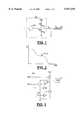
- FIG. 1illustrates a conventional output buffer coupled to a transmission line
- FIG. 2illustrates the output voltage of an output buffer as it undergoes an output transition from a high state to a low state while driving a transmission line load.
- the circuit 150generally comprises a transistor P1, a transistor N1, a transistor N2, a transistor N3, a transistor N4, an inverter 152, a pad 154 and a voltage source 160.
- a gate of the transistor P1generally receives an input signal INP.
- the source of the transistor P1is generally coupled to a supply voltage VCC.
- the drain of the transistor P1is generally coupled to the pad 154 as well as to drains of the transistors N1, N3 and N2.
- the sources of the transistors N1, N2 and N4are generally coupled to ground GND.
- the pulldown transistor N2is generally connected as a diode when the transistor N3 is turned on or can be completely turned off by turning on the transistor N4.
- the initial driveis generally provided by the transistors N1 and N2.
- the gate voltage on the transistor N2needs to be around 2V when the pad may be at 1V. This may insure that the combined impedance of N1 and N2 is generally low enough with respect to the impedance of the transmission line such that the plateau is generally at or below the desired 1V load.
- the precise relationship between the pad voltage and the gate voltage on transistor N2may be controlled by the voltage source follower 160 shown in FIG. 3. Such a voltage source follower on the chip may be implemented in many different ways in order to meet the design criteria of a particular application.
- the transistor N2begins to shut off. Reducing the gate voltage on the transistor N2 significantly below 2V (i.e. to around 1.5V or below) will effectively turn off the transistor N2 and may dramatically increase its impedance.
- the transistor MN1When the output circuit 150 is driving a logic 1, the transistor MN1 is generally on, the transistor MN2 is generally off, the transistor MN4 is generally on and the transistor MN3 is generally off.
- the transistor MP1will generally be off and the node N1 will generally be disconnected from the supply voltage VCC.
- the transistor MN5is generally on so that the node N2 will be connected to the supply voltage VSS.
- the transistors MP2 and MP3will generally be on (but there is generally no current through them since the transistor MP1 is off).
- the node N1will be at a voltage between ground (VSS) and VTP above VSS since the transistors MP2 and MP3 are generally considered to be configured as diodes.
- the transistor MP5Since there may be leakage currents, the transistor MP5 will generally be in a hard off state since the gate of the transistor MP5 is generally connected to the output pad 154.
- the transistor MP4will also be off when the transistor MP5 is in a hard off state.
- the transistor MN2will pull the voltage at the output pad 154 toward the supply voltage VSS fairly rapidly. Additional edge rate control circuits may be implemented to reduce noise on the chip due to the output switching in order to meet the design criteria of a particular application. The fact that the transistors MN3 turns on much later than the transistor MN2 may also help to control noise (e.g., ground bounce).
- noisee.g., ground bounce
- the impedance of the circuit 150is generally a function of the transistors MN2 and MN3 (which is generally controlled by the voltage at the output pad 154), the impedance of the circuit 150 generally varies upwards as the voltage at the output pad 154 varies downwards. After a transition, the voltage at the output pad 154 will reach a level near the ground voltage VSS. The transistor MN5 will then shut off stopping the flow of current through the current mirror 164 of the transistors MP3 and MP2. The transistor MP4 will never shut off completely. Hence the transistor MP5 gradually turns on and will connect the gates of the current mirror 164 to the node N1. When this happens the leakage currents through the current mirror 164 are generally eliminated.
Landscapes
- Physics & Mathematics (AREA)
- Engineering & Computer Science (AREA)
- Computer Hardware Design (AREA)
- Computing Systems (AREA)
- General Engineering & Computer Science (AREA)
- Mathematical Physics (AREA)
- Logic Circuits (AREA)
Abstract
Description
Claims (17)
Priority Applications (1)
| Application Number | Priority Date | Filing Date | Title |
|---|---|---|---|
| US08/837,782US5917335A (en) | 1997-04-22 | 1997-04-22 | Output voltage controlled impedance output buffer |
Applications Claiming Priority (1)
| Application Number | Priority Date | Filing Date | Title |
|---|---|---|---|
| US08/837,782US5917335A (en) | 1997-04-22 | 1997-04-22 | Output voltage controlled impedance output buffer |
Publications (1)
| Publication Number | Publication Date |
|---|---|
| US5917335Atrue US5917335A (en) | 1999-06-29 |
Family
ID=25275410
Family Applications (1)
| Application Number | Title | Priority Date | Filing Date |
|---|---|---|---|
| US08/837,782Expired - LifetimeUS5917335A (en) | 1997-04-22 | 1997-04-22 | Output voltage controlled impedance output buffer |
Country Status (1)
| Country | Link |
|---|---|
| US (1) | US5917335A (en) |
Cited By (10)
| Publication number | Priority date | Publication date | Assignee | Title |
|---|---|---|---|---|
| US6141258A (en)* | 1998-12-11 | 2000-10-31 | Kabushki Kaisha Toshiba | Programmable impedance output buffer drivers, semiconductor devices and static random access memories provided with a progammable impedance output port |
| US6175250B1 (en)* | 1996-09-24 | 2001-01-16 | Telefonaktiebolaget L M Ericsson (Publ) | Output buffer circuit for driving a transmission line |
| US6184730B1 (en) | 1999-11-03 | 2001-02-06 | Pericom Semiconductor Corp. | CMOS output buffer with negative feedback dynamic-drive control and dual P,N active-termination transmission gates |
| US6426653B1 (en) | 1997-09-29 | 2002-07-30 | Cypress Semiconductor Corp. | MOS output driver, and circuit and method of controlling same |
| US7202699B1 (en) | 2003-09-15 | 2007-04-10 | Cypress Semiconductor Corporation | Voltage tolerant input buffer |
| US7394293B1 (en) | 2003-09-25 | 2008-07-01 | Cypress Semiconductor Corp. | Circuit and method for rapid power up of a differential output driver |
| US7479800B1 (en) | 2005-09-29 | 2009-01-20 | Cypress Semiconductor Corporation | Variable impedance sense architecture and method |
| US20090085614A1 (en)* | 2007-09-27 | 2009-04-02 | Suresh Parameswaran | Circuits and methods for programming integrated circuit input and output impedances |
| US7888962B1 (en) | 2004-07-07 | 2011-02-15 | Cypress Semiconductor Corporation | Impedance matching circuit |
| US8036846B1 (en) | 2005-10-20 | 2011-10-11 | Cypress Semiconductor Corporation | Variable impedance sense architecture and method |
Citations (34)
| Publication number | Priority date | Publication date | Assignee | Title |
|---|---|---|---|---|
| US3878483A (en)* | 1973-10-12 | 1975-04-15 | Us Navy | Voltage-tunable, seven-decade, continuously-variable oscillator |
| US4484149A (en)* | 1980-02-12 | 1984-11-20 | Analog Devices, Inc. | Single-supply IC digital-to-analog converter for use with microprocessors |
| US4514704A (en)* | 1983-08-26 | 1985-04-30 | Curtis Douglas R | Variable filter circuit |
| US4543561A (en)* | 1980-02-12 | 1985-09-24 | Analog Devices, Incorporated | Single-supply IC digital-to-analog converter for use with microprocessors |
| US4627085A (en)* | 1984-06-29 | 1986-12-02 | Applied Micro Circuits Corporation | Flip-flop control circuit |
| US4684831A (en)* | 1984-08-21 | 1987-08-04 | Applied Micro Circuits Corporation | Level shift circuit for interfacing between two different voltage levels using a current mirror circuit |
| US4736125A (en)* | 1986-08-28 | 1988-04-05 | Applied Micro Circuits Corporation | Unbuffered TTL-to-ECL translator with temperature-compensated threshold voltage obtained from a constant-current reference voltage |
| US4751404A (en)* | 1986-10-31 | 1988-06-14 | Applied Micro Circuits Corporation | Multi-level ECL series gating with temperature-stabilized source current |
| US4769589A (en)* | 1987-11-04 | 1988-09-06 | Teledyne Industries, Inc. | Low-voltage, temperature compensated constant current and voltage reference circuit |
| US4800298A (en)* | 1987-08-04 | 1989-01-24 | Motorola, Inc. | Output buffer for improving di/dt |
| EP0317271A2 (en)* | 1987-11-17 | 1989-05-24 | Applied Micro Circuits Corporation | Method and apparatus for coupling an ECL output signal using a clamped capacitive bootstrap circuit |
| US4835420A (en)* | 1987-11-17 | 1989-05-30 | Applied Micro Circuits Corporation | Method and apparatus for signal level conversion with clamped capacitive bootstrap |
| US4845385A (en)* | 1988-06-21 | 1989-07-04 | Silicon Connections Corporation | BiCMOS logic circuits with reduced crowbar current |
| US4875003A (en)* | 1989-02-21 | 1989-10-17 | Silicon Connections Corporation | Non-contact I/O signal pad scan testing of VLSI circuits |
| US4874970A (en)* | 1988-05-11 | 1989-10-17 | Applied Micro Circuits Corporation | ECL output with Darlington or common collector-common emitter drive |
| US4876216A (en)* | 1988-03-07 | 1989-10-24 | Applied Micro Circuits Corporation | Semiconductor integrated circuit manufacturing process providing oxide-filled trench isolation of circuit devices |
| US4954769A (en)* | 1989-02-08 | 1990-09-04 | Burr-Brown Corporation | CMOS voltage reference and buffer circuit |
| US4970414A (en)* | 1989-07-07 | 1990-11-13 | Silicon Connections Corporation | TTL-level-output interface circuit |
| US4972101A (en)* | 1989-09-19 | 1990-11-20 | Digital Equipment Corporation | Noise reduction in CMOS driver using capacitor discharge to generate a control voltage |
| US5027013A (en)* | 1987-11-17 | 1991-06-25 | Applied Micro Circuits Corporation | Method and apparatus for coupling an ECL output signal using a clamped capacitive bootstrap circuit |
| US5036222A (en)* | 1990-02-22 | 1991-07-30 | National Semiconductor Corporation | Output buffer circuit with output voltage sensing for reducing switching induced noise |
| US5047711A (en)* | 1989-08-23 | 1991-09-10 | Silicon Connections Corporation | Wafer-level burn-in testing of integrated circuits |
| US5097148A (en)* | 1990-04-25 | 1992-03-17 | At&T Bell Laboratories | Integrated circuit buffer with improved drive capability |
| US5212440A (en)* | 1990-05-14 | 1993-05-18 | Micron Technology, Inc. | Quick response CMOS voltage reference circuit |
| US5245273A (en)* | 1991-10-30 | 1993-09-14 | Motorola, Inc. | Bandgap voltage reference circuit |
| US5252909A (en)* | 1991-01-25 | 1993-10-12 | Nec Corporation | Constant-voltage generating circuit |
| US5272395A (en)* | 1991-04-05 | 1993-12-21 | Analog Devices, Inc. | CMOS strobed comparator |
| US5424629A (en)* | 1991-04-11 | 1995-06-13 | Matsushita Electric Industrial Co., Ltd. | Power circuit for a semiconductor apparatus |
| US5448182A (en)* | 1994-05-02 | 1995-09-05 | Motorola Inc. | Driver circuit with self-adjusting impedance matching |
| US5457407A (en)* | 1994-07-06 | 1995-10-10 | Sony Electronics Inc. | Binary weighted reference circuit for a variable impedance output buffer |
| US5514979A (en)* | 1994-11-28 | 1996-05-07 | Unisys Corporation | Methods and apparatus for dynamically reducing ringing of driver output signal |
| US5528166A (en)* | 1995-03-14 | 1996-06-18 | Intel Corporation | Pulse controlled impedance compensated output buffer |
| US5559447A (en)* | 1994-11-17 | 1996-09-24 | Cypress Semiconductor | Output buffer with variable output impedance |
| US5726589A (en)* | 1995-11-01 | 1998-03-10 | International Business Machines Corporation | Off-chip driver circuit with reduced hot-electron degradation |
- 1997
- 1997-04-22USUS08/837,782patent/US5917335A/ennot_activeExpired - Lifetime
Patent Citations (36)
| Publication number | Priority date | Publication date | Assignee | Title |
|---|---|---|---|---|
| US3878483A (en)* | 1973-10-12 | 1975-04-15 | Us Navy | Voltage-tunable, seven-decade, continuously-variable oscillator |
| US4484149A (en)* | 1980-02-12 | 1984-11-20 | Analog Devices, Inc. | Single-supply IC digital-to-analog converter for use with microprocessors |
| US4543561A (en)* | 1980-02-12 | 1985-09-24 | Analog Devices, Incorporated | Single-supply IC digital-to-analog converter for use with microprocessors |
| US4514704A (en)* | 1983-08-26 | 1985-04-30 | Curtis Douglas R | Variable filter circuit |
| US4627085A (en)* | 1984-06-29 | 1986-12-02 | Applied Micro Circuits Corporation | Flip-flop control circuit |
| US4684831A (en)* | 1984-08-21 | 1987-08-04 | Applied Micro Circuits Corporation | Level shift circuit for interfacing between two different voltage levels using a current mirror circuit |
| US4736125A (en)* | 1986-08-28 | 1988-04-05 | Applied Micro Circuits Corporation | Unbuffered TTL-to-ECL translator with temperature-compensated threshold voltage obtained from a constant-current reference voltage |
| US4751404A (en)* | 1986-10-31 | 1988-06-14 | Applied Micro Circuits Corporation | Multi-level ECL series gating with temperature-stabilized source current |
| US4800298A (en)* | 1987-08-04 | 1989-01-24 | Motorola, Inc. | Output buffer for improving di/dt |
| US4769589A (en)* | 1987-11-04 | 1988-09-06 | Teledyne Industries, Inc. | Low-voltage, temperature compensated constant current and voltage reference circuit |
| EP0317271A2 (en)* | 1987-11-17 | 1989-05-24 | Applied Micro Circuits Corporation | Method and apparatus for coupling an ECL output signal using a clamped capacitive bootstrap circuit |
| US4835420A (en)* | 1987-11-17 | 1989-05-30 | Applied Micro Circuits Corporation | Method and apparatus for signal level conversion with clamped capacitive bootstrap |
| US4926065A (en)* | 1987-11-17 | 1990-05-15 | Applied Micro Circuits Corporation | Method and apparatus for coupling an ECL output signal using a clamped capacitive bootstrap circuit |
| US5027013A (en)* | 1987-11-17 | 1991-06-25 | Applied Micro Circuits Corporation | Method and apparatus for coupling an ECL output signal using a clamped capacitive bootstrap circuit |
| US4876216A (en)* | 1988-03-07 | 1989-10-24 | Applied Micro Circuits Corporation | Semiconductor integrated circuit manufacturing process providing oxide-filled trench isolation of circuit devices |
| US4874970A (en)* | 1988-05-11 | 1989-10-17 | Applied Micro Circuits Corporation | ECL output with Darlington or common collector-common emitter drive |
| US4845385A (en)* | 1988-06-21 | 1989-07-04 | Silicon Connections Corporation | BiCMOS logic circuits with reduced crowbar current |
| US4954769A (en)* | 1989-02-08 | 1990-09-04 | Burr-Brown Corporation | CMOS voltage reference and buffer circuit |
| US4875003A (en)* | 1989-02-21 | 1989-10-17 | Silicon Connections Corporation | Non-contact I/O signal pad scan testing of VLSI circuits |
| US4970414A (en)* | 1989-07-07 | 1990-11-13 | Silicon Connections Corporation | TTL-level-output interface circuit |
| US5047711A (en)* | 1989-08-23 | 1991-09-10 | Silicon Connections Corporation | Wafer-level burn-in testing of integrated circuits |
| US4972101A (en)* | 1989-09-19 | 1990-11-20 | Digital Equipment Corporation | Noise reduction in CMOS driver using capacitor discharge to generate a control voltage |
| US5036222A (en)* | 1990-02-22 | 1991-07-30 | National Semiconductor Corporation | Output buffer circuit with output voltage sensing for reducing switching induced noise |
| EP0443435B1 (en)* | 1990-02-22 | 1995-10-25 | National Semiconductor Corporation | Output buffer circuit with output voltage sensing for reducing switching induced noise |
| US5097148A (en)* | 1990-04-25 | 1992-03-17 | At&T Bell Laboratories | Integrated circuit buffer with improved drive capability |
| US5212440A (en)* | 1990-05-14 | 1993-05-18 | Micron Technology, Inc. | Quick response CMOS voltage reference circuit |
| US5252909A (en)* | 1991-01-25 | 1993-10-12 | Nec Corporation | Constant-voltage generating circuit |
| US5272395A (en)* | 1991-04-05 | 1993-12-21 | Analog Devices, Inc. | CMOS strobed comparator |
| US5424629A (en)* | 1991-04-11 | 1995-06-13 | Matsushita Electric Industrial Co., Ltd. | Power circuit for a semiconductor apparatus |
| US5245273A (en)* | 1991-10-30 | 1993-09-14 | Motorola, Inc. | Bandgap voltage reference circuit |
| US5448182A (en)* | 1994-05-02 | 1995-09-05 | Motorola Inc. | Driver circuit with self-adjusting impedance matching |
| US5457407A (en)* | 1994-07-06 | 1995-10-10 | Sony Electronics Inc. | Binary weighted reference circuit for a variable impedance output buffer |
| US5559447A (en)* | 1994-11-17 | 1996-09-24 | Cypress Semiconductor | Output buffer with variable output impedance |
| US5514979A (en)* | 1994-11-28 | 1996-05-07 | Unisys Corporation | Methods and apparatus for dynamically reducing ringing of driver output signal |
| US5528166A (en)* | 1995-03-14 | 1996-06-18 | Intel Corporation | Pulse controlled impedance compensated output buffer |
| US5726589A (en)* | 1995-11-01 | 1998-03-10 | International Business Machines Corporation | Off-chip driver circuit with reduced hot-electron degradation |
Non-Patent Citations (2)
| Title |
|---|
| Gomez, D., Specifying the ASIC Tester, EE Times, n503, T5, 1988, pp. 1 5.* |
| Gomez, D., Specifying the ASIC Tester, EE Times, n503, T5, 1988, pp. 1-5. |
Cited By (11)
| Publication number | Priority date | Publication date | Assignee | Title |
|---|---|---|---|---|
| US6175250B1 (en)* | 1996-09-24 | 2001-01-16 | Telefonaktiebolaget L M Ericsson (Publ) | Output buffer circuit for driving a transmission line |
| US6426653B1 (en) | 1997-09-29 | 2002-07-30 | Cypress Semiconductor Corp. | MOS output driver, and circuit and method of controlling same |
| US6141258A (en)* | 1998-12-11 | 2000-10-31 | Kabushki Kaisha Toshiba | Programmable impedance output buffer drivers, semiconductor devices and static random access memories provided with a progammable impedance output port |
| US6184730B1 (en) | 1999-11-03 | 2001-02-06 | Pericom Semiconductor Corp. | CMOS output buffer with negative feedback dynamic-drive control and dual P,N active-termination transmission gates |
| US7202699B1 (en) | 2003-09-15 | 2007-04-10 | Cypress Semiconductor Corporation | Voltage tolerant input buffer |
| US7394293B1 (en) | 2003-09-25 | 2008-07-01 | Cypress Semiconductor Corp. | Circuit and method for rapid power up of a differential output driver |
| US7888962B1 (en) | 2004-07-07 | 2011-02-15 | Cypress Semiconductor Corporation | Impedance matching circuit |
| US7479800B1 (en) | 2005-09-29 | 2009-01-20 | Cypress Semiconductor Corporation | Variable impedance sense architecture and method |
| US8036846B1 (en) | 2005-10-20 | 2011-10-11 | Cypress Semiconductor Corporation | Variable impedance sense architecture and method |
| US20090085614A1 (en)* | 2007-09-27 | 2009-04-02 | Suresh Parameswaran | Circuits and methods for programming integrated circuit input and output impedances |
| US8040164B2 (en) | 2007-09-27 | 2011-10-18 | Cypress Semiconductor Corporation | Circuits and methods for programming integrated circuit input and output impedances |
Similar Documents
| Publication | Publication Date | Title |
|---|---|---|
| US5568062A (en) | Low noise tri-state output buffer | |
| US5559447A (en) | Output buffer with variable output impedance | |
| US5594370A (en) | High performance backplane driver circuit | |
| EP0329285B1 (en) | Output buffer | |
| US5347177A (en) | System for interconnecting VLSI circuits with transmission line characteristics | |
| US5488322A (en) | Digital interface circuit with dual switching points for increased speed | |
| US6420913B1 (en) | Dynamic termination logic driver with improved impedance control | |
| US5894238A (en) | Output buffer with static and transient pull-up and pull-down drivers | |
| US6351172B1 (en) | High-speed output driver with an impedance adjustment scheme | |
| US6215342B1 (en) | Power-on reset circuit for dual-supply system | |
| US6911860B1 (en) | On/off reference voltage switch for multiple I/O standards | |
| US5828262A (en) | Ultra low power pumped n-channel output buffer with self-bootstrap | |
| US6255867B1 (en) | CMOS output buffer with feedback control on sources of pre-driver stage | |
| JPH07170168A (en) | Output circuit and operation method | |
| JPH0936673A (en) | Compensated-off bias voltage feeding circuit | |
| US6316957B1 (en) | Method for a dynamic termination logic driver with improved impedance control | |
| KR19990067849A (en) | Voltage tolerant output buffer | |
| US5914844A (en) | Overvoltage-tolerant input-output buffers having a switch configured to isolate a pull up transistor from a voltage supply | |
| US6294924B1 (en) | Dynamic termination logic driver with improved slew rate control | |
| US5097148A (en) | Integrated circuit buffer with improved drive capability | |
| US5917335A (en) | Output voltage controlled impedance output buffer | |
| US7876129B2 (en) | Load sense and active noise reduction for I/O circuit | |
| US6265931B1 (en) | Voltage reference source for an overvoltage-tolerant bus interface | |
| US6225819B1 (en) | Transmission line impedance matching output buffer | |
| US7276939B2 (en) | Semiconductor integrated circuit |
Legal Events
| Date | Code | Title | Description |
|---|---|---|---|
| AS | Assignment | Owner name:CYPRESS SEMICONDUCTOR CORPORATION, CALIFORNIA Free format text:ASSIGNMENT OF ASSIGNORS INTEREST;ASSIGNOR:REES, DAVID B.;REEL/FRAME:008675/0557 Effective date:19970420 | |
| STCF | Information on status: patent grant | Free format text:PATENTED CASE | |
| FPAY | Fee payment | Year of fee payment:4 | |
| FPAY | Fee payment | Year of fee payment:8 | |
| REMI | Maintenance fee reminder mailed | ||
| FPAY | Fee payment | Year of fee payment:12 | |
| SULP | Surcharge for late payment | Year of fee payment:11 | |
| AS | Assignment | Owner name:MORGAN STANLEY SENIOR FUNDING, INC., NEW YORK Free format text:SECURITY INTEREST;ASSIGNORS:CYPRESS SEMICONDUCTOR CORPORATION;SPANSION LLC;REEL/FRAME:035240/0429 Effective date:20150312 | |
| AS | Assignment | Owner name:SPANSION LLC, CALIFORNIA Free format text:PARTIAL RELEASE OF SECURITY INTEREST IN PATENTS;ASSIGNOR:MORGAN STANLEY SENIOR FUNDING, INC., AS COLLATERAL AGENT;REEL/FRAME:039708/0001 Effective date:20160811 Owner name:CYPRESS SEMICONDUCTOR CORPORATION, CALIFORNIA Free format text:PARTIAL RELEASE OF SECURITY INTEREST IN PATENTS;ASSIGNOR:MORGAN STANLEY SENIOR FUNDING, INC., AS COLLATERAL AGENT;REEL/FRAME:039708/0001 Effective date:20160811 | |
| AS | Assignment | Owner name:MONTEREY RESEARCH, LLC, CALIFORNIA Free format text:ASSIGNMENT OF ASSIGNORS INTEREST;ASSIGNOR:CYPRESS SEMICONDUCTOR CORPORATION;REEL/FRAME:040911/0238 Effective date:20160811 | |
| AS | Assignment | Owner name:MORGAN STANLEY SENIOR FUNDING, INC., NEW YORK Free format text:CORRECTIVE ASSIGNMENT TO CORRECT THE 8647899 PREVIOUSLY RECORDED ON REEL 035240 FRAME 0429. ASSIGNOR(S) HEREBY CONFIRMS THE SECURITY INTERST;ASSIGNORS:CYPRESS SEMICONDUCTOR CORPORATION;SPANSION LLC;REEL/FRAME:058002/0470 Effective date:20150312 |