US5917216A - Trenched field effect transistor with PN depletion barrier - Google Patents
Trenched field effect transistor with PN depletion barrierDownload PDFInfo
- Publication number
- US5917216A US5917216AUS08/742,326US74232696AUS5917216AUS 5917216 AUS5917216 AUS 5917216AUS 74232696 AUS74232696 AUS 74232696AUS 5917216 AUS5917216 AUS 5917216A
- Authority
- US
- United States
- Prior art keywords
- region
- trenches
- semiconductor material
- trench
- conductivity type
- Prior art date
- Legal status (The legal status is an assumption and is not a legal conclusion. Google has not performed a legal analysis and makes no representation as to the accuracy of the status listed.)
- Expired - Lifetime
Links
Images


Classifications
- H—ELECTRICITY
- H10—SEMICONDUCTOR DEVICES; ELECTRIC SOLID-STATE DEVICES NOT OTHERWISE PROVIDED FOR
- H10D—INORGANIC ELECTRIC SEMICONDUCTOR DEVICES
- H10D30/00—Field-effect transistors [FET]
- H10D30/60—Insulated-gate field-effect transistors [IGFET]
- H10D30/64—Double-diffused metal-oxide semiconductor [DMOS] FETs
- H10D30/66—Vertical DMOS [VDMOS] FETs
- H10D30/668—Vertical DMOS [VDMOS] FETs having trench gate electrodes, e.g. UMOS transistors
- H—ELECTRICITY
- H10—SEMICONDUCTOR DEVICES; ELECTRIC SOLID-STATE DEVICES NOT OTHERWISE PROVIDED FOR
- H10D—INORGANIC ELECTRIC SEMICONDUCTOR DEVICES
- H10D30/00—Field-effect transistors [FET]
- H10D30/60—Insulated-gate field-effect transistors [IGFET]
- H10D30/63—Vertical IGFETs
- H—ELECTRICITY
- H10—SEMICONDUCTOR DEVICES; ELECTRIC SOLID-STATE DEVICES NOT OTHERWISE PROVIDED FOR
- H10D—INORGANIC ELECTRIC SEMICONDUCTOR DEVICES
- H10D30/00—Field-effect transistors [FET]
- H10D30/60—Insulated-gate field-effect transistors [IGFET]
- H10D30/63—Vertical IGFETs
- H10D30/635—Vertical IGFETs having no inversion channels, e.g. vertical accumulation channel FETs [ACCUFET] or normally-on vertical IGFETs
- H—ELECTRICITY
- H10—SEMICONDUCTOR DEVICES; ELECTRIC SOLID-STATE DEVICES NOT OTHERWISE PROVIDED FOR
- H10D—INORGANIC ELECTRIC SEMICONDUCTOR DEVICES
- H10D30/00—Field-effect transistors [FET]
- H10D30/60—Insulated-gate field-effect transistors [IGFET]
- H10D30/611—Insulated-gate field-effect transistors [IGFET] having multiple independently-addressable gate electrodes influencing the same channel
- H10D30/615—Insulated-gate field-effect transistors [IGFET] having multiple independently-addressable gate electrodes influencing the same channel comprising a MOS gate electrode and at least one non-MOS gate electrode
- H—ELECTRICITY
- H10—SEMICONDUCTOR DEVICES; ELECTRIC SOLID-STATE DEVICES NOT OTHERWISE PROVIDED FOR
- H10D—INORGANIC ELECTRIC SEMICONDUCTOR DEVICES
- H10D62/00—Semiconductor bodies, or regions thereof, of devices having potential barriers
- H10D62/10—Shapes, relative sizes or dispositions of the regions of the semiconductor bodies; Shapes of the semiconductor bodies
- H10D62/102—Constructional design considerations for preventing surface leakage or controlling electric field concentration
- H10D62/103—Constructional design considerations for preventing surface leakage or controlling electric field concentration for increasing or controlling the breakdown voltage of reverse-biased devices
- H10D62/105—Constructional design considerations for preventing surface leakage or controlling electric field concentration for increasing or controlling the breakdown voltage of reverse-biased devices by having particular doping profiles, shapes or arrangements of PN junctions; by having supplementary regions, e.g. junction termination extension [JTE]
- H10D62/106—Constructional design considerations for preventing surface leakage or controlling electric field concentration for increasing or controlling the breakdown voltage of reverse-biased devices by having particular doping profiles, shapes or arrangements of PN junctions; by having supplementary regions, e.g. junction termination extension [JTE] having supplementary regions doped oppositely to or in rectifying contact with regions of the semiconductor bodies, e.g. guard rings with PN or Schottky junctions
- H—ELECTRICITY
- H10—SEMICONDUCTOR DEVICES; ELECTRIC SOLID-STATE DEVICES NOT OTHERWISE PROVIDED FOR
- H10D—INORGANIC ELECTRIC SEMICONDUCTOR DEVICES
- H10D62/00—Semiconductor bodies, or regions thereof, of devices having potential barriers
- H10D62/10—Shapes, relative sizes or dispositions of the regions of the semiconductor bodies; Shapes of the semiconductor bodies
- H10D62/13—Semiconductor regions connected to electrodes carrying current to be rectified, amplified or switched, e.g. source or drain regions
- H10D62/149—Source or drain regions of field-effect devices
- H10D62/151—Source or drain regions of field-effect devices of IGFETs
- H10D62/156—Drain regions of DMOS transistors
- H10D62/157—Impurity concentrations or distributions
- H—ELECTRICITY
- H10—SEMICONDUCTOR DEVICES; ELECTRIC SOLID-STATE DEVICES NOT OTHERWISE PROVIDED FOR
- H10D—INORGANIC ELECTRIC SEMICONDUCTOR DEVICES
- H10D62/00—Semiconductor bodies, or regions thereof, of devices having potential barriers
- H10D62/10—Shapes, relative sizes or dispositions of the regions of the semiconductor bodies; Shapes of the semiconductor bodies
- H10D62/17—Semiconductor regions connected to electrodes not carrying current to be rectified, amplified or switched, e.g. channel regions
- H10D62/213—Channel regions of field-effect devices
- H10D62/221—Channel regions of field-effect devices of FETs
- H10D62/235—Channel regions of field-effect devices of FETs of IGFETs
Definitions
- This inventionpertains to transistors, and more specifically to a field effect transistor having its gate electrode located in a trench and being suitable for use in integrated circuits or as a discrete component, especially for use as a power transistor.
- FETsField effect transistors
- MOSFETsmetal oxide semiconductor field effect transistors
- R DSon-state resistance
- an output rectifiersupports 20 volts for a 3.3 volt output and 10 volts for a 1.5 volt output.
- Schottky rectifiersare used but these disadvantageously have forward voltage drops of about 0.5 volts, which degrades the efficiency of the power supply.
- a power MOSFETshould have the lowest possible on-state specific resistance to minimize conduction losses.
- On-state resistanceis a well known parameter of the efficiency of a power switching transistor and is a ratio of drain to source voltage to drain current when the device is fully turned on.
- On-state specific resistancerefers to resistance times cross sectional area of the substrate carrying the drain current.
- FIG. 1aA typical prior art N-channel trenched MOSFET is shown in FIG. 1a, having conductive gate electrode 10 typically being N doped polycrystalline silicon (N type polysilicon) which is doped to be conductive serving as a gate electrode and located in a trench 12, the floor and sidewalls of which are insulated by a layer of gate oxide 16. Oxide layer 18 insulates the upper portion of gate electrode 10.
- the metallized source contact 20contacts both the N+ doped source region 24 formed in the upper portion of the device and the P doped body region 38.
- the drain electrode 28is a metallized contact to the N+ drain region 30 at the bottom surface of the device.
- N- doped drift region 34typically formed by epitaxy (hence an epitaxial layer) and being the drift region.
- the upper portion of the epitaxial layeris P doped to form the body region 38 and the very upper portion of the epitaxial layer is N+ doped to form the source region 24.
- this transistoris typically formed in a silicon wafer and moreover there are a number of gate trenches 12 arranged (in a plan view) in rectangles, circles, hexagons, or linear structures, each defining a cell and all cells typically having a common source contact and a common gate contact.
- the trench 12extends only partly through the N- doped drift region 34 and does not extend into the N+ doped drain region 30.
- the blocking stateis ordinarily the state when the transistor is off, i.e. not conducting current, and a measure of blocking capability is leakage current. Ideally, leakage current is zero.
- This transistorhas an inferior on-state specific resistance to the ideal due to the substantial resistance of the N-doped drift region 34 below the trench.
- FIG. 1bshows an N-channel device called the ACCUFET as described in "The Accumulation Mode Field Effect Transistor: A New UltraLow On-Resistance MOSFET" by Baliga et al., IEEE ELECTRON DEVICE LETTERS, Vol. 13, No. 8, August 1992.
- the ACCUFETis an ultra-low on-state specific resistance vertical channel power MOSFET structure which uses current conduction via an accumulation layer formed on the surface of the trench gate structure.
- the ACCUFETdoes not contain a P body region 38, unlike the transistor of FIG. 1a, and the gate trench 42 extends all the way into the highly doped drain region 30.
- the polysiliconis P doped and the N-region 34 is very lightly doped.
- the optimum N- drift region doping for a conventional MOSFET of FIG. 1ais typically 2 ⁇ 10 16 /cm 3
- the N- region dopingis typically below 10 14 /cm 3 .
- the doping type of the conventional MOSFET polysilicon gate electrodeis typically N-type, and not P-type.
- the ACCUFET on-state specific resistanceis 105 micro-ohm cm 2 at a gate bias of 15 volts.
- the ACCUFETis described as having an on-state specific resistance which is the lowest attainable for any known MOS gate-control device.
- the ACCUFETis bidirectional, i.e. reversal of the source and drain contacts in use is available.
- the ACCUFET blocking characteristicsare less than might be desired, and negative gate voltages are required to reduce leakage current to acceptable levels.
- a trenched semiconductor deviceincludes relatively lightly doped regions having in cross section the shape of "ears" formed extending laterally from the trench sidewalls, intermediate of the source region and the trench floors. These ears are of opposite doping type to that of the adjacent region and have typical doping concentration of 10 13 to 10 18 /cm 3 .
- the earsare a PN depletion barrier layer, and in the on-state they become inverted at the surface of the trench gate structure.
- the deviceconducts current through the accumulation region and the inverted depletion barrier region at the surface of the trench gate structure. Blocking is achieved in the off-state by gate control depletion of the adjacent N-region and by the PN depletion barrier layer.
- the doping type of the polysilicon gate electrodelike that of the ACCUFET, is opposite to that of the source region and drain region.
- this devicehas been found to have superior on-state specific resistance to that of a conventional MOS trench device, with an on-state specific resistance similar to that of the ACCUFET.
- the present devicehas superior voltage blocking characteristics to those of the ACCUFET due to the inclusion of the depletion barrier layer, and, unlike the ACCUFET, acceptable levels of leakage current are maintained at zero gate bias. Additionally, the present device has bidirectional characteristics with pentode characteristics obtainable with current flow from drain to source when V DS (source-drain voltage) is greater than zero, and with current flow from source to drain when V DS is less than zero.
- the PN depletion barrier layerIn the blocking state the PN depletion barrier layer is fully or almost fully depleted; thus, the undesirable properties of a floating, undepleted PN junction are avoided.
- the PN junctionIn the conventional N-channel MOSFET the PN junction is part of a parasitic NPN transistor which, if not effectively shorted, will lead to device destruction if current is generated by avalanche breakdown. Avalanche breakdown occurs when voltages, and hence electric fields, become large enough to create large amounts of hole-electron current due to impact ionization.
- the blocking characteristics of the present deviceare determined by barrier-limited majority carrier current flow and not by avalanche breakdown.
- the present PN junctionmay float, i.e. remain unshorted, availing bidirectional characteristics.
- the depletion barrier layermay be of various shapes and in various locations between the source region (which is near the semiconductor device principal surface) and the drain region (which is at the lower portion of the semiconductor device).
- the depletion barrier layermay be located immediately below the source region or adjacent the trench floors or intermediate thereof.
- the depletion barrier layermay extend all the way from one trench to an adjacent trench or only part way, so long as it is located near the sidewalls of each trench. There may be multiple such depletion barrier layers stacked vertically.
- the depletion barrier layermay be of various widths and heights and doping levels.
- the depletion barrier layeris formed by a double trench etch process in which the gate trenches are etched to a first depth. Then the depletion barrier layer is implanted through the trench floors and driven in to extend laterally into the substrate. Then a second etch step deepens the trenches, eliminating the portion of the driven-in implant at the trench floors and leaving only the "ears" adjacent to the newly etched trench sidewalls. The device is then completed conventionally.
- the depletion barrier layeris located immediately below the source region and is formed instead by implanting the depletion barrier layer with a high energy implant, followed by etching the trench through the implant. This leaves only the "ear" regions of the implant serving as the depletion barrier layer. This process does not require the double trench etch of the other process.
- Other processesalso may be used for fabricating the presently disclosed structures.
- FIG. 1ashows a prior art N-channel MOSFET.
- FIG. 1bshows a prior art ACCUFET.
- FIG. 2shows in cross section an N-channel MOSFET in accordance with the present invention.
- FIG. 3shows current conduction in the MOSFET of FIG. 2.
- FIG. 4shows a depletion profile of the MOSFET of FIG. 2.
- FIG. 5shows a conduction band barrier profile of the MOSFET of FIG. 2.
- FIG. 6shows dimensions of the MOSFET of FIG. 2.
- FIG. 7shows a P-channel MOSFET complementary to that of FIG. 2.
- FIG. 8shows a MOSFET having multiple depletion barrier regions in accordance with the present invention.
- FIG. 9shows another MOSFET in accordance with the present invention having a Schottky contact to the source regions.
- FIG. 10shows another MOSFET in accordance with the present invention illustrating an epitaxial layer/substrate interface.
- FIG. 11shows another MOSFET in accordance with the present invention illustrating the trench penetrating into the lower portion of the substrate.
- FIGS. 12a-12cshow steps in fabrication of a MOSFET in accordance with the present invention.
- FIG. 13shows another MOSFET in accordance with the present invention with the barrier layer immediately under the source region.
- FIG. 14shows another MOSFET in accordance with the present invention with the barrier layer located immediately under the source region.
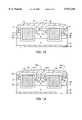
- FIG. 2shows a cross-section of a trenched N-channel MOSFET in accordance with the present invention.
- FIG. 2like the other figures herein, is not to scale and that furthermore the various doped semiconductor regions shown herein, which are shown as precisely defined regions delineated by lines, are conventional representations of doped regions having gradient dopant levels at their edges.
- typically power MOSFETsinclude a large number of cells, the cells having various shapes such as square, circular, hexagonal, linear or others. These cells are evident in a top side view (not provided here); in terms of cell layout, the present MOSFETs are conventional and may be fabricated in any one of a number of well known cell structures. The present depictions are therefore typically of only one cell or a portion of two cells as delineated by the gate trenches, and are not intended to illustrate an entire power transistor which would typically include hundreds or thousands of such cells.
- the N-channel MOSFET of FIG. 2is in most respects similar to that of the N-channel ACCUFET of FIG. 1b (and referred to by identical reference numbers) with the important addition of the P doped depletion barrier layer regions extending from the sidewalls of the trenches into the drift region and having a P-doped polysilicon gate electrode.
- the depletion barrier layer for each trench 42a,42bis in two portions respectively 50-1, 50-2 and 50-3, 50-4 which appear in cross section to be "ears" extending from the trench sidewalls.
- This barrier layer 50-1, 50-2, 50-3, 50-4is a major distinction between the MOSFET of FIG. 2 and the prior art ACCUFET.
- This barrier layerprovides the advantage of surface conduction as depicted in the FIG. 3, which is depicted along the FIG. 2 MOSFET trench sidewall and shows current flow for the on-state conduction path from the N+ doped drain region 30 through the accumulation region, through the inversion region (formed within the depletion barrier layer) layer 50-2 through the upper accumulation region, through the upper portion of the lightly doped drift region 34 through the N+ source region 24 to the N+ source region contact 20.
- FIG. 4Operation of the device of FIG. 2 in the blocking state, i.e., where V GS is equal to zero, is depicted in FIG. 4, showing the depletion region in the P depletion barrier layer (negative charge) and in the N- region (positive charge).
- FIG. 5A corresponding conduction band barrier profile with V DS greater than zero and V GS equal to zero is shown in FIG. 5, where the vertical axis is the energy E C and the horizontal axis is the linear dimension along line XX in FIG. 4.
- the PN depletion barrier layer(designated “PN-barrier”) provides a conduction band energy “hump” in the blocking state, hence advantageously reducing leakage current and improving (increasing) blocking voltage.
- the indication “qV DS " of the right hand side of FIG. 5indicates the total energy is a function of charge (q) multiplied by V DS .
- the depletion barrier layeris totally depleted.
- the typical undesirable parasitic NPN transistorwhich appears in a prior art MOSFET as in FIG. 1a is not present here, due to depletion.
- a MOSFET including the present depletion barrier layer and gate electrode doping typeexhibits significant improvement in blocking voltage capability compared to the ACCUFET for instance.
- An ACCUFEThas been compared to the present MOSFET, at a blocking voltage of 15 volts.
- the leakage current for the ACCUFETwas found to be approximately 10 times greater than that for the present MOSFET.
- V GSis equal to zero, at a blocking voltage of as little as 8 volts, whereas a similar leakage current would only occur for the present MOSFET at a blocking voltage of 15 volts.
- the present deviceis clearly superior to the ACCUFET in this regard. Also it has been found that on-state resistance for the present MOSFET is approximately the same as for comparable ACCUFETS. Hence, a superior blocking capability is achieved at no disadvantage in terms of specific on resistance compared to the ACCUFET.
- the particular shape of the depletion barrier layer as shown in FIG. 2is not critical to the present invention, nor is its extent. That is, the depletion barrier layer may be located anywhere along the sidewalls of the gate trenches and may extend all the way from the sidewall of one trench to the sidewall of the adjacent trench, and need not extend exactly to the sidewall but may be spaced slightly apart therefrom, so long as the depletion improvement is still present. Moreover, the height (vertical extent) of the depletion barrier layer need not be any particular amount so long as it is adequate to provide the desired blocking capability. A wide range of doping levels of the depletion barrier layer also provides the desired depletion effect.
- FIG. 6shows a somewhat schematic depiction of the structure of FIG. 2 with some structures eliminated or redrawn for simplicity, so as to depict relevant illustrative dimensions and doping (concentration) levels.
- the dimension Lwhich is the trench depth, is in the range of 0.2 to 10 microns ( ⁇ m).
- the dimension Wwhich is the spacing between adjacent trenches, is also in the range of 0.2 to 10 microns.
- the width of the trenches, which is dimension Dis in the range of 0.2 to 10 microns.
- Dimension Ywhich is the height of the depletion barrier layer 50-1, 50-2, 50-3, 50-4 may be any dimension greater than zero and less than L and typically is in the range of 0.2 to 2 microns.
- the dimension Xwhich is the spacing between adjacent portions of the depletion barrier layer, is in the range zero (indicating that the depletion barrier layer extends from trench to trench) to slightly less than dimension W, in which case the width of the depletion barrier layer portions is minimal.
- a minimal width of each "ear”is e.g. 0.1 micron.
- Dimension Zwhich is the depth of the depletion barrier layer relative to the principal surface of the substrate, is in the range of zero (immediately below the source region) to L, in which case the barrier layer is located adjacent the floors of the trenches.
- the dopant concentration levels of portions of the present devicemay vary, as is typical of MOSFETs and well understood to one in the art.
- the doping level N S of the N+ source region 24is in the range of 10 17 to 10 22 /cm 3 .
- the doping level N C of the N- lightly doped drift region 34is in the range of 10 13 to 10 16 /cm 3 .
- the doping level of the P depletion barrier layer 50-1, etc.is in the range of 10 13 to 10 18 /cm 3 .
- the usual P type dopantis boron, but this is not limiting; neither are the above-mentioned concentration levels.
- FIG. 7shows a P-channel MOSFET complementary in conductivity types to that of FIG. 2. This device would have the same benefits as those of FIG. 2 and would operate similarly.
- the substrate 60is P+ doped while the lightly doped region 62 is P- doped and the source regions 66 are P+ doped.
- the depletion barrier layer 68-1, 68-2, 68-3,is N doped.
- the polysilicon gate electrodes 64a, 64bare N doped, in contrast to the P doping of the polysilicon gate electrode in the N-channel device of FIG. 2.
- FIG. 8shows (somewhat schematically) a cross section of a MOSFET in accordance with the present invention having a plurality of depletion barrier layers in substrate 80.
- barrier layers NB 1 , NB 2 , NB 3which are at varying depths respectively z 1 , z 2 and z 3 .
- there are three barrier layers NB 1 , NB 2 , NB 3each potentially varying in height, respectively heights y 1 , y 2 and y 3 , and each having a spacing between the two opposing "ears", in respectively spacings x 1 , x 2 and x 3 .
- each barrier layermay have its own dimensions.
- Use of multiple depletion barrier layerwould include in one version one depletion barrier layer near the top of the trench and one near the bottom of the trench, to provide symmetry for bidirectional characteristics.
- Such a devicewould be fabricated e.g. by multiple ion implants at different energies.
- FIG. 9shows another embodiment in accordance with the present invention otherwise similar to that of FIG. 2, except that the N+ doped source region is modified so that it is formed in two portions 84-1, 84-2, separated by a portion of the N- region 34.
- a Schottky contact 88is made ohmically to the source regions 84-1, 84-2 and drift region 34.
- Such a Schottky contactis well known in the art and in this application improves the barrier at the surface of the device. The advantage of this is to extend the barrier into the portion of the N- region 34 between the N+ source regions 84-1, 84-2.
- FIG. 10shows somewhat schematically yet another embodiment in accordance with the present invention.
- the depletion barrier layer 50-1, 50-2, 50-3is as in FIG. 2; however, in this case the trenches 90a, 90b do not penetrate all the way down to the upper portion of the N+ drain region 30, but instead only extend down partly through the N- region 34 (which is in this case an epitaxial layer).
- the dimension t between the floor of the trenches 90a, 90b and the upper portion of the N+ drain region 30may be any dimension, as determined by process or other limitations.
- This structureallows the depletion barrier to extend down further below the trench floors into the lower portion of the region 34. The advantage of this is increased blocking capability, at the expense of on-state specific resistance.
- FIG. 11shows yet another embodiment in accordance with the present invention.
- the trenches 92a, 92bextend down into the lower portion of the device, i.e. into the N+ drain region 30 by a depth t which may be any dimension as determined by the maximum trench depth.
- the advantage of thisis to guarantee extension of the trench into the drain region.
- FIGS. 12a through 12cshow process steps to fabricate the MOSFET of FIG. 2 (and with readily apparent modifications the MOSFETs of FIGS. 7, 8, 9, 10, and 11). These steps individually are conventional.
- FIG. 12abegins with an N+ doped substrate 30, on which is grown an N- doped epitaxial layer 34 having a thickness of 2 microns. Then a "hard” mask (for instance oxide) is formed over the principal surface of layer 34 and patterned into portions 98a, 98b, 98c to define the trench openings. Then the trenches are anisotropically etched to form the straight sided trenches 42a, 42b shown.
- a "hard” maskfor instance oxide
- boronis implanted at an energy level in the range of 30 to 80 KEV and driven in to form the P doped depletion barrier layer 50 having a doping concentration in the range of 10 13 to 10 18 /cm 3 , as described above.
- the hard mask 98a, 98b, 98cextending between each two adjacent trenches prevents the boron atoms from being implanted immediately below the mask 98a, 98b, 98c; however, the drive in step drives the boron atoms so that they extend laterally beyond the trench sidewalls.
- the extent to which the boron atoms extend laterallyis determined by the implant energy and the drive in step parameters, thus determining how close the two adjacent portions of the depletion barrier layer approach one another after drive in.
- a second etch stepis performed using the same hard mask as before to extend the trenches 42a, 42b downward further through the implanted P depletion barrier layer 50, thus eliminating a substantial part of P layer 50 but leaving the characteristic "ears" 50-1, 50-2, 50-3, 50-4 extending from the sidewalls of each trench.
- this structurecan be identified with that of FIG. 2.
- the transistoris then completed conventionally (not shown) by stripping off the hard mask 98a, 98b, 98c, growing the gate oxide, filling the trenches with polysilicon, doping the polysilicon, patterning the polysilicon to form the gate electrodes, and then using a mask to form the N+ source regions (not shown).
- the passivationis formed, and then the metallization is formed to contact the source region and the drain region as shown in FIG. 2.
- FIG. 13shows yet another embodiment fabricated by a process different from that shown in FIGS. 12a to 12c but similar in structure to that of FIG. 2, except that the depletion barrier layer 50-1, 50-2, 50-3, 50-4 is not formed midway on the sidewalls of the trenches 42a, 42b, but instead is formed adjacent the upper portion of the trench sidewalls and immediately below the N+ source regions 24. It has been found that this structure provides the benefits of the depletion barrier layer without the need for the double trench etch steps of FIG. 12.
- FIG. 14A variant of the MOSFET of FIG. 13 is shown in FIG. 14.
- the P depletion barrier layer 50-1, 50-2, 50-3, 50-4 formed adjacent the upper portions of the trench sidewallsthere is also a P+ region 100-1, 100-2 adjacent the principal surface of the substrate and located between each two portions of the source region.
- This P+ regionin combination with the adjacent source region, forms a PN diode and increases the barrier laterally and vertically.
- the depletion barrier layeris formed by a high energy implant so as to be located immediately below the N+ doped source regions 24 and has a typical doping level of 10 16 /cm 3 or less.
- the N- region 34has a typical doping level of 10 14 /cm 3 .
- the trenchesare formed by a conventional single trench etch process.
- the P depletion barrier layer 50-1, 50-2, 50-3, 50-4is implanted (using a suitable separate mask) prior to etching the trenches. The trenches are then etched through the P depletion barrier layer.
- termination isolationprevents drain to source shorting.
- an isolation structurefor a closed cell MOSFET
- the terminationincludes dummy cells (having no source contact).
- the polysilicon gate structures in the dummy cellsare isolated from the active cell gate structures.
- termination isolation moatsare provided to close off the ends of the cells.
Landscapes
- Electrodes Of Semiconductors (AREA)
- Metal-Oxide And Bipolar Metal-Oxide Semiconductor Integrated Circuits (AREA)
Abstract
Description
Claims (14)
Priority Applications (1)
| Application Number | Priority Date | Filing Date | Title |
|---|---|---|---|
| US08/742,326US5917216A (en) | 1995-02-10 | 1996-10-31 | Trenched field effect transistor with PN depletion barrier |
Applications Claiming Priority (2)
| Application Number | Priority Date | Filing Date | Title |
|---|---|---|---|
| US38662095A | 1995-02-10 | 1995-02-10 | |
| US08/742,326US5917216A (en) | 1995-02-10 | 1996-10-31 | Trenched field effect transistor with PN depletion barrier |
Related Parent Applications (1)
| Application Number | Title | Priority Date | Filing Date |
|---|---|---|---|
| US38662095AContinuation | 1995-02-10 | 1995-02-10 |
Publications (1)
| Publication Number | Publication Date |
|---|---|
| US5917216Atrue US5917216A (en) | 1999-06-29 |
Family
ID=23526359
Family Applications (1)
| Application Number | Title | Priority Date | Filing Date |
|---|---|---|---|
| US08/742,326Expired - LifetimeUS5917216A (en) | 1995-02-10 | 1996-10-31 | Trenched field effect transistor with PN depletion barrier |
Country Status (3)
| Country | Link |
|---|---|
| US (1) | US5917216A (en) |
| EP (1) | EP0726603B1 (en) |
| DE (1) | DE69602114T2 (en) |
Cited By (64)
| Publication number | Priority date | Publication date | Assignee | Title |
|---|---|---|---|---|
| US6198127B1 (en)* | 1999-05-19 | 2001-03-06 | Intersil Corporation | MOS-gated power device having extended trench and doping zone and process for forming same |
| US6380569B1 (en)* | 1999-08-10 | 2002-04-30 | Rockwell Science Center, Llc | High power unipolar FET switch |
| US6396084B1 (en) | 1998-08-31 | 2002-05-28 | Fairchild Korea Semiconductor Ltd | Structure of semiconductor rectifier |
| WO2002027800A3 (en)* | 2000-09-28 | 2002-06-13 | Gen Semiconductor Inc | Trench dmos transistor having lightly doped source structure |
| US6498382B2 (en)* | 2000-03-24 | 2002-12-24 | Infineon Technologies Ag | Semiconductor configuration |
| US20030047793A1 (en)* | 2001-09-07 | 2003-03-13 | Power Integrations, Inc. | High-voltage vertical transistor with a multi-layered extended drain structure |
| US20030047792A1 (en)* | 2001-09-07 | 2003-03-13 | Power Integrations, Inc. | High-voltage lateral transistor with a multi-layered extended drain structure |
| US20030060001A1 (en)* | 2001-09-07 | 2003-03-27 | Power Integrations, Inc. | Method of fabricating a high-voltage transistor with a multi-layered extended drain structure |
| US6573559B2 (en)* | 2000-03-01 | 2003-06-03 | Shindengen Electric Manufacturing Co., Ltd. | Transistor and method of manufacturing the same |
| US20030155577A1 (en)* | 1997-06-11 | 2003-08-21 | Seiko Epson Corporation | Semiconductor device, liquid crystal display, and electronic equipment including the same |
| US20040021173A1 (en)* | 2002-07-30 | 2004-02-05 | Fairchild Semiconductor Corporation | Dual trench power mosfet |
| US6710418B1 (en) | 2002-10-11 | 2004-03-23 | Fairchild Semiconductor Corporation | Schottky rectifier with insulation-filled trenches and method of forming the same |
| US6798016B2 (en)* | 1996-04-22 | 2004-09-28 | International Rectifier Corporation | Trench MOS device and process for radhard device |
| US6803626B2 (en) | 2002-07-18 | 2004-10-12 | Fairchild Semiconductor Corporation | Vertical charge control semiconductor device |
| US20050073030A1 (en)* | 2002-12-03 | 2005-04-07 | Kabushiki Kaisha Toshiba | Semiconductor device having rectifying action |
| US20050133858A1 (en)* | 2001-09-07 | 2005-06-23 | Power Integrations, Inc. | High-voltage vertical transistor with a multi-gradient drain doping profile |
| US6916745B2 (en) | 2003-05-20 | 2005-07-12 | Fairchild Semiconductor Corporation | Structure and method for forming a trench MOSFET having self-aligned features |
| US20050242392A1 (en)* | 2004-04-30 | 2005-11-03 | Siliconix Incorporated | Super trench MOSFET including buried source electrode and method of fabricating the same |
| US6991977B2 (en) | 2001-10-17 | 2006-01-31 | Fairchild Semiconductor Corporation | Method for forming a semiconductor structure with improved smaller forward voltage loss and higher blocking capability |
| US7033891B2 (en) | 2002-10-03 | 2006-04-25 | Fairchild Semiconductor Corporation | Trench gate laterally diffused MOSFET devices and methods for making such devices |
| US7061066B2 (en) | 2001-10-17 | 2006-06-13 | Fairchild Semiconductor Corporation | Schottky diode using charge balance structure |
| US7132712B2 (en) | 2002-11-05 | 2006-11-07 | Fairchild Semiconductor Corporation | Trench structure having one or more diodes embedded therein adjacent a PN junction |
| US7265416B2 (en) | 2002-02-23 | 2007-09-04 | Fairchild Korea Semiconductor Ltd. | High breakdown voltage low on-resistance lateral DMOS transistor |
| US7265415B2 (en) | 2004-10-08 | 2007-09-04 | Fairchild Semiconductor Corporation | MOS-gated transistor with reduced miller capacitance |
| US7301203B2 (en) | 2003-11-28 | 2007-11-27 | Fairchild Korea Semiconductor Ltd. | Superjunction semiconductor device |
| US7319256B1 (en) | 2006-06-19 | 2008-01-15 | Fairchild Semiconductor Corporation | Shielded gate trench FET with the shield and gate electrodes being connected together |
| US20080061390A1 (en)* | 2006-09-11 | 2008-03-13 | Pradyumna Kumar Swain | Method and Apparatus for Reducing Smear in Back-Illuminated Imaging Sensors |
| US7345342B2 (en) | 2001-01-30 | 2008-03-18 | Fairchild Semiconductor Corporation | Power semiconductor devices and methods of manufacture |
| US7352036B2 (en) | 2004-08-03 | 2008-04-01 | Fairchild Semiconductor Corporation | Semiconductor power device having a top-side drain using a sinker trench |
| US7368777B2 (en) | 2003-12-30 | 2008-05-06 | Fairchild Semiconductor Corporation | Accumulation device with charge balance structure and method of forming the same |
| US7385248B2 (en) | 2005-08-09 | 2008-06-10 | Fairchild Semiconductor Corporation | Shielded gate field effect transistor with improved inter-poly dielectric |
| US20080197417A1 (en)* | 2007-02-16 | 2008-08-21 | Power Integrations, Inc. | Segmented pillar layout for a high-voltage vertical transistor |
| US20080197406A1 (en)* | 2007-02-16 | 2008-08-21 | Power Integrations, Inc. | Sensing FET integrated with a high-voltage vertical transistor |
| US20080197397A1 (en)* | 2007-02-16 | 2008-08-21 | Power Integrations, Inc. | Checkerboarded high-voltage vertical transistor layout |
| US20080197418A1 (en)* | 2007-02-16 | 2008-08-21 | Power Integrations, Inc. | Gate pullback at ends of high-voltage vertical transistor structure |
| US7446374B2 (en) | 2006-03-24 | 2008-11-04 | Fairchild Semiconductor Corporation | High density trench FET with integrated Schottky diode and method of manufacture |
| US7468536B2 (en) | 2007-02-16 | 2008-12-23 | Power Integrations, Inc. | Gate metal routing for transistor with checkerboarded layout |
| US7504306B2 (en) | 2005-04-06 | 2009-03-17 | Fairchild Semiconductor Corporation | Method of forming trench gate field effect transistor with recessed mesas |
| US7576388B1 (en) | 2002-10-03 | 2009-08-18 | Fairchild Semiconductor Corporation | Trench-gate LDMOS structures |
| US20090218619A1 (en)* | 2008-03-02 | 2009-09-03 | Alpha & Omega Semiconductor, Ltd | Self-aligned slotted accumulation-mode field effect transistor (AccuFET) structure and method |
| US7625793B2 (en) | 1999-12-20 | 2009-12-01 | Fairchild Semiconductor Corporation | Power MOS device with improved gate charge performance |
| US7638841B2 (en) | 2003-05-20 | 2009-12-29 | Fairchild Semiconductor Corporation | Power semiconductor devices and methods of manufacture |
| US7745289B2 (en) | 2000-08-16 | 2010-06-29 | Fairchild Semiconductor Corporation | Method of forming a FET having ultra-low on-resistance and low gate charge |
| US7772668B2 (en) | 2007-12-26 | 2010-08-10 | Fairchild Semiconductor Corporation | Shielded gate trench FET with multiple channels |
| US7786533B2 (en) | 2001-09-07 | 2010-08-31 | Power Integrations, Inc. | High-voltage vertical transistor with edge termination structure |
| US7791136B1 (en)* | 2009-04-23 | 2010-09-07 | Force Mos Technology Co., Ltd. | Trench MOSFET having trench contacts integrated with trench Schottky rectifiers having planar contacts |
| US20110215399A1 (en)* | 2010-03-03 | 2011-09-08 | Renesas Electronics Corporation | P-channel power mosfet |
| US8319290B2 (en) | 2010-06-18 | 2012-11-27 | Fairchild Semiconductor Corporation | Trench MOS barrier schottky rectifier with a planar surface using CMP techniques |
| US8673700B2 (en) | 2011-04-27 | 2014-03-18 | Fairchild Semiconductor Corporation | Superjunction structures for power devices and methods of manufacture |
| US20140117415A1 (en)* | 2012-10-30 | 2014-05-01 | Chengdu Monolithic Power Systems Co., Ltd. | Junction field effect transistors and associated fabrication methods |
| US8723317B2 (en)* | 2012-09-14 | 2014-05-13 | Force Mos Technology Co., Ltd. | Trench metal oxide semiconductor field effect transistor with embedded schottky rectifier using reduced masks process |
| US8772868B2 (en) | 2011-04-27 | 2014-07-08 | Fairchild Semiconductor Corporation | Superjunction structures for power devices and methods of manufacture |
| US8786010B2 (en) | 2011-04-27 | 2014-07-22 | Fairchild Semiconductor Corporation | Superjunction structures for power devices and methods of manufacture |
| US8829641B2 (en) | 2001-01-30 | 2014-09-09 | Fairchild Semiconductor Corporation | Method of forming a dual-trench field effect transistor |
| US8836028B2 (en) | 2011-04-27 | 2014-09-16 | Fairchild Semiconductor Corporation | Superjunction structures for power devices and methods of manufacture |
| US8928077B2 (en) | 2007-09-21 | 2015-01-06 | Fairchild Semiconductor Corporation | Superjunction structures for power devices |
| US8963212B2 (en) | 2008-12-08 | 2015-02-24 | Fairchild Semiconductor Corporation | Trench-based power semiconductor devices with increased breakdown voltage characteristics |
| US9024328B2 (en) | 2013-07-02 | 2015-05-05 | General Electric Company | Metal-oxide-semiconductor (MOS) devices with increased channel periphery and methods of manufacture |
| US9431481B2 (en) | 2008-09-19 | 2016-08-30 | Fairchild Semiconductor Corporation | Superjunction structures for power devices and methods of manufacture |
| US9543396B2 (en) | 2013-12-13 | 2017-01-10 | Power Integrations, Inc. | Vertical transistor device structure with cylindrically-shaped regions |
| US9748341B2 (en) | 2013-07-02 | 2017-08-29 | General Electric Company | Metal-oxide-semiconductor (MOS) devices with increased channel periphery |
| US20180286742A1 (en)* | 2017-03-30 | 2018-10-04 | United Microelectronics Corp. | Semiconductor structure capable of improving row hammer effect in dynamic random access memory and fabrication method thereof |
| US10325988B2 (en) | 2013-12-13 | 2019-06-18 | Power Integrations, Inc. | Vertical transistor device structure with cylindrically-shaped field plates |
| JP2022553305A (en)* | 2019-10-21 | 2022-12-22 | ロベルト・ボッシュ・ゲゼルシャフト・ミト・ベシュレンクテル・ハフツング | Vertical field effect transistor and method of forming the same |
Families Citing this family (6)
| Publication number | Priority date | Publication date | Assignee | Title |
|---|---|---|---|---|
| JP4167313B2 (en)* | 1997-03-18 | 2008-10-15 | 株式会社東芝 | High voltage power semiconductor device |
| GB9820904D0 (en)* | 1998-09-26 | 1998-11-18 | Koninkl Philips Electronics Nv | Bi-directional semiconductor switch and switch circuit for battery-powered equipment |
| DE10001869B4 (en)* | 2000-01-18 | 2006-10-26 | Infineon Technologies Ag | In both directions blocking controllable semiconductor switching element |
| US6555895B1 (en)* | 2000-07-17 | 2003-04-29 | General Semiconductor, Inc. | Devices and methods for addressing optical edge effects in connection with etched trenches |
| DE102010063314B4 (en) | 2010-12-17 | 2022-10-13 | Robert Bosch Gmbh | Semiconductor device with improved avalanche resistance |
| CN109545839B (en)* | 2018-11-12 | 2021-08-24 | 东南大学 | A bidirectional withstand voltage VDMOS device |
Citations (17)
| Publication number | Priority date | Publication date | Assignee | Title |
|---|---|---|---|---|
| US4434433A (en)* | 1977-02-21 | 1984-02-28 | Zaidan Hojin Handotai Kenkyu Shinkokai | Enhancement mode JFET dynamic memory |
| US4791462A (en)* | 1987-09-10 | 1988-12-13 | Siliconix Incorporated | Dense vertical j-MOS transistor |
| US4835586A (en)* | 1987-09-21 | 1989-05-30 | Siliconix Incorporated | Dual-gate high density fet |
| US4914058A (en)* | 1987-12-29 | 1990-04-03 | Siliconix Incorporated | Grooved DMOS process with varying gate dielectric thickness |
| US5021845A (en)* | 1985-08-30 | 1991-06-04 | Texas Instruments Incorporated | Semiconductor device and process fabrication thereof |
| JPH03195064A (en)* | 1989-12-25 | 1991-08-26 | Nippon Telegr & Teleph Corp <Ntt> | MOS field effect transistor |
| US5164325A (en)* | 1987-10-08 | 1992-11-17 | Siliconix Incorporated | Method of making a vertical current flow field effect transistor |
| US5168331A (en)* | 1991-01-31 | 1992-12-01 | Siliconix Incorporated | Power metal-oxide-semiconductor field effect transistor |
| US5177572A (en)* | 1990-04-06 | 1993-01-05 | Nissan Motor Co., Ltd. | Mos device using accumulation layer as channel |
| EP0583023A1 (en)* | 1992-08-12 | 1994-02-16 | SILICONIX Incorporated | Trenched DMOS transistor fabrication using six masks |
| US5350934A (en)* | 1992-03-05 | 1994-09-27 | Kabushiki Kaisha Toshiba | Conductivity modulation type insulated gate field effect transistor |
| US5405794A (en)* | 1994-06-14 | 1995-04-11 | Philips Electronics North America Corporation | Method of producing VDMOS device of increased power density |
| US5410170A (en)* | 1993-04-14 | 1995-04-25 | Siliconix Incorporated | DMOS power transistors with reduced number of contacts using integrated body-source connections |
| US5430315A (en)* | 1993-07-22 | 1995-07-04 | Rumennik; Vladimir | Bi-directional power trench MOS field effect transistor having low on-state resistance and low leakage current |
| US5473176A (en)* | 1993-09-01 | 1995-12-05 | Kabushiki Kaisha Toshiba | Vertical insulated gate transistor and method of manufacture |
| US5474943A (en)* | 1993-03-15 | 1995-12-12 | Siliconix Incorporated | Method for fabricating a short channel trenched DMOS transistor |
| US5488236A (en)* | 1994-05-26 | 1996-01-30 | North Carolina State University | Latch-up resistant bipolar transistor with trench IGFET and buried collector |
- 1996
- 1996-02-06EPEP96300793Apatent/EP0726603B1/ennot_activeExpired - Lifetime
- 1996-02-06DEDE69602114Tpatent/DE69602114T2/ennot_activeExpired - Fee Related
- 1996-10-31USUS08/742,326patent/US5917216A/ennot_activeExpired - Lifetime
Patent Citations (17)
| Publication number | Priority date | Publication date | Assignee | Title |
|---|---|---|---|---|
| US4434433A (en)* | 1977-02-21 | 1984-02-28 | Zaidan Hojin Handotai Kenkyu Shinkokai | Enhancement mode JFET dynamic memory |
| US5021845A (en)* | 1985-08-30 | 1991-06-04 | Texas Instruments Incorporated | Semiconductor device and process fabrication thereof |
| US4791462A (en)* | 1987-09-10 | 1988-12-13 | Siliconix Incorporated | Dense vertical j-MOS transistor |
| US4835586A (en)* | 1987-09-21 | 1989-05-30 | Siliconix Incorporated | Dual-gate high density fet |
| US5164325A (en)* | 1987-10-08 | 1992-11-17 | Siliconix Incorporated | Method of making a vertical current flow field effect transistor |
| US4914058A (en)* | 1987-12-29 | 1990-04-03 | Siliconix Incorporated | Grooved DMOS process with varying gate dielectric thickness |
| JPH03195064A (en)* | 1989-12-25 | 1991-08-26 | Nippon Telegr & Teleph Corp <Ntt> | MOS field effect transistor |
| US5177572A (en)* | 1990-04-06 | 1993-01-05 | Nissan Motor Co., Ltd. | Mos device using accumulation layer as channel |
| US5168331A (en)* | 1991-01-31 | 1992-12-01 | Siliconix Incorporated | Power metal-oxide-semiconductor field effect transistor |
| US5350934A (en)* | 1992-03-05 | 1994-09-27 | Kabushiki Kaisha Toshiba | Conductivity modulation type insulated gate field effect transistor |
| EP0583023A1 (en)* | 1992-08-12 | 1994-02-16 | SILICONIX Incorporated | Trenched DMOS transistor fabrication using six masks |
| US5474943A (en)* | 1993-03-15 | 1995-12-12 | Siliconix Incorporated | Method for fabricating a short channel trenched DMOS transistor |
| US5410170A (en)* | 1993-04-14 | 1995-04-25 | Siliconix Incorporated | DMOS power transistors with reduced number of contacts using integrated body-source connections |
| US5430315A (en)* | 1993-07-22 | 1995-07-04 | Rumennik; Vladimir | Bi-directional power trench MOS field effect transistor having low on-state resistance and low leakage current |
| US5473176A (en)* | 1993-09-01 | 1995-12-05 | Kabushiki Kaisha Toshiba | Vertical insulated gate transistor and method of manufacture |
| US5488236A (en)* | 1994-05-26 | 1996-01-30 | North Carolina State University | Latch-up resistant bipolar transistor with trench IGFET and buried collector |
| US5405794A (en)* | 1994-06-14 | 1995-04-11 | Philips Electronics North America Corporation | Method of producing VDMOS device of increased power density |
Non-Patent Citations (14)
| Title |
|---|
| Baliga, B., et al., "The Accumulation-Mode Field-Effect Transistor: A New Ultralow On-Resistance MOSFET," IEEE Electron Device Letters, vol. 13, No. 8, Aug. 1992, pp. 427-429. |
| Baliga, B., et al., The Accumulation Mode Field Effect Transistor: A New Ultralow On Resistance MOSFET, IEEE Electron Device Letters, vol. 13, No. 8, Aug. 1992, pp. 427 429.* |
| K. Sunouchi et al. "A Surrounding Gate Transistor (SGT) Cell for 64/256 Mbit DRAM s," IEDM Technical Digest 1989, pp. 2.1.1-2.1.4. |
| K. Sunouchi et al. A Surrounding Gate Transistor (SGT) Cell for 64/256 Mbit DRAM s, IEDM Technical Digest 1989, pp. 2.1.1 2.1.4.* |
| Mader, H., "Electrical Properties of Bulk-Barrier Diodes," IEEE Transactions on Electron Devices, vol. ED-29, No. 11, Nov. 1982, pp. 1766-1771. |
| Mader, H., Electrical Properties of Bulk Barrier Diodes, IEEE Transactions on Electron Devices, vol. ED 29, No. 11, Nov. 1982, pp. 1766 1771.* |
| Mader, H., et al., "Bulk-Barrier Transistor," IEEE Transactions on Electron Devices, vol. ED-30, No. 10, Oct. 1983, pp. 1380-1386. |
| Mader, H., et al., Bulk Barrier Transistor, IEEE Transactions on Electron Devices, vol. ED 30, No. 10, Oct. 1983, pp. 1380 1386.* |
| McCowen, A., et al., "Gate controlled bulk-barrier mechanism in an MOS power transistor," IEEE Proceedings, vol. 134, Pt. I, No. 6, Dec. 1987, pp. 165-169. |
| McCowen, A., et al., Gate controlled bulk barrier mechanism in an MOS power transistor, IEEE Proceedings, vol. 134, Pt. I, No. 6, Dec. 1987, pp. 165 169.* |
| S. Watanabe et al. "A Novel Circuit Technology with Surrounding Gate Transistor (SGT's) for Ultra High Density DRAM's," IEEE Journal of Solid-State Circuits, vol. 30, No. 9, Sep. 1995, pp. 960-970. |
| S. Watanabe et al. A Novel Circuit Technology with Surrounding Gate Transistor (SGT s) for Ultra High Density DRAM s, IEEE Journal of Solid State Circuits, vol. 30, No. 9, Sep. 1995, pp. 960 970.* |
| Syau, T., et al., "Comparison of Ultralow Specific On-Resistance Umosfet Structures: The ACCUFET, EXTFET, INVFET, and Conventional UMOSET's," IEEE Transactions on Electron Devices, vol. 41, No. 5, May 1994, pp. 800-808. |
| Syau, T., et al., Comparison of Ultralow Specific On Resistance Umosfet Structures: The ACCUFET, EXTFET, INVFET, and Conventional UMOSET s, IEEE Transactions on Electron Devices, vol. 41, No. 5, May 1994, pp. 800 808.* |
Cited By (163)
| Publication number | Priority date | Publication date | Assignee | Title |
|---|---|---|---|---|
| US6798016B2 (en)* | 1996-04-22 | 2004-09-28 | International Rectifier Corporation | Trench MOS device and process for radhard device |
| US20030155577A1 (en)* | 1997-06-11 | 2003-08-21 | Seiko Epson Corporation | Semiconductor device, liquid crystal display, and electronic equipment including the same |
| US6396084B1 (en) | 1998-08-31 | 2002-05-28 | Fairchild Korea Semiconductor Ltd | Structure of semiconductor rectifier |
| US6198127B1 (en)* | 1999-05-19 | 2001-03-06 | Intersil Corporation | MOS-gated power device having extended trench and doping zone and process for forming same |
| US6380569B1 (en)* | 1999-08-10 | 2002-04-30 | Rockwell Science Center, Llc | High power unipolar FET switch |
| US7625793B2 (en) | 1999-12-20 | 2009-12-01 | Fairchild Semiconductor Corporation | Power MOS device with improved gate charge performance |
| US6573559B2 (en)* | 2000-03-01 | 2003-06-03 | Shindengen Electric Manufacturing Co., Ltd. | Transistor and method of manufacturing the same |
| US6498382B2 (en)* | 2000-03-24 | 2002-12-24 | Infineon Technologies Ag | Semiconductor configuration |
| US8710584B2 (en) | 2000-08-16 | 2014-04-29 | Fairchild Semiconductor Corporation | FET device having ultra-low on-resistance and low gate charge |
| US8101484B2 (en) | 2000-08-16 | 2012-01-24 | Fairchild Semiconductor Corporation | Method of forming a FET having ultra-low on-resistance and low gate charge |
| US7745289B2 (en) | 2000-08-16 | 2010-06-29 | Fairchild Semiconductor Corporation | Method of forming a FET having ultra-low on-resistance and low gate charge |
| US6445037B1 (en) | 2000-09-28 | 2002-09-03 | General Semiconductor, Inc. | Trench DMOS transistor having lightly doped source structure |
| CN1552101B (en)* | 2000-09-28 | 2010-06-16 | 通用半导体公司 | Recessed DMOS Transistor with Lightly Doped Source Structure |
| WO2002027800A3 (en)* | 2000-09-28 | 2002-06-13 | Gen Semiconductor Inc | Trench dmos transistor having lightly doped source structure |
| US7345342B2 (en) | 2001-01-30 | 2008-03-18 | Fairchild Semiconductor Corporation | Power semiconductor devices and methods of manufacture |
| US8829641B2 (en) | 2001-01-30 | 2014-09-09 | Fairchild Semiconductor Corporation | Method of forming a dual-trench field effect transistor |
| US9368587B2 (en) | 2001-01-30 | 2016-06-14 | Fairchild Semiconductor Corporation | Accumulation-mode field effect transistor with improved current capability |
| US20070293002A1 (en)* | 2001-09-07 | 2007-12-20 | Power Intergrations, Inc. | Method of fabricating a high-voltage transistor with an extended drain structure |
| US6987299B2 (en) | 2001-09-07 | 2006-01-17 | Power Integrations, Inc. | High-voltage lateral transistor with a multi-layered extended drain structure |
| US6781198B2 (en) | 2001-09-07 | 2004-08-24 | Power Integrations, Inc. | High-voltage vertical transistor with a multi-layered extended drain structure |
| US20040082122A1 (en)* | 2001-09-07 | 2004-04-29 | Power Integrations, Inc. | Method of fabricating a high-voltage transistor with a multi-layered extended drain structure |
| US6798020B2 (en) | 2001-09-07 | 2004-09-28 | Power Integrations, Inc. | High-voltage lateral transistor with a multi-layered extended drain structure |
| US7829944B2 (en) | 2001-09-07 | 2010-11-09 | Power Integrations, Inc. | High-voltage vertical transistor with a multi-layered extended drain structure |
| US6815293B2 (en) | 2001-09-07 | 2004-11-09 | Power Intergrations, Inc. | High-voltage lateral transistor with a multi-layered extended drain structure |
| US20040232486A1 (en)* | 2001-09-07 | 2004-11-25 | Power Integrations, Inc. | High-voltage lateral transistor with a multi-layered extended drain structure |
| US6838346B2 (en)* | 2001-09-07 | 2005-01-04 | Power Integrations, Inc. | Method of fabricating a high-voltage transistor with a multi-layered extended drain structure |
| US20050023571A1 (en)* | 2001-09-07 | 2005-02-03 | Power Integrations, Inc. | High-voltage vertical transistor with a multi-layered extended drain structure |
| US20090233407A1 (en)* | 2001-09-07 | 2009-09-17 | Power Integrations, Inc. | Method of fabricating a high-voltage transistor with an extended drain structure |
| US20050104121A1 (en)* | 2001-09-07 | 2005-05-19 | Power Integrations, Inc. | Method of fabricating a high-voltage transistor with an extended drain structure |
| US20050133858A1 (en)* | 2001-09-07 | 2005-06-23 | Power Integrations, Inc. | High-voltage vertical transistor with a multi-gradient drain doping profile |
| US7459366B2 (en) | 2001-09-07 | 2008-12-02 | Power Integrations, Inc. | High-voltage vertical transistor with a multi-gradient drain doping profile |
| US8940605B2 (en) | 2001-09-07 | 2015-01-27 | Power Integrations, Inc. | Method of fabricating a high-voltage transistor with an extended drain structure |
| US7745291B2 (en) | 2001-09-07 | 2010-06-29 | Power Integrations, Inc. | Method of fabricating a high-voltage transistor with an extended drain structure |
| US20080102581A1 (en)* | 2001-09-07 | 2008-05-01 | Power Integrations, Inc. | High-voltage vertical transistor with a multi-gradient drain doping profile |
| US20110018058A1 (en)* | 2001-09-07 | 2011-01-27 | Power Integrations, Inc. | High-voltage vertical transistor with edge termination structure |
| US20030151110A1 (en)* | 2001-09-07 | 2003-08-14 | Power Integrations, Inc. | High-voltage lateral transistor with a multi-layered extended drain structure |
| US7786533B2 (en) | 2001-09-07 | 2010-08-31 | Power Integrations, Inc. | High-voltage vertical transistor with edge termination structure |
| US20030047793A1 (en)* | 2001-09-07 | 2003-03-13 | Power Integrations, Inc. | High-voltage vertical transistor with a multi-layered extended drain structure |
| US20030047792A1 (en)* | 2001-09-07 | 2003-03-13 | Power Integrations, Inc. | High-voltage lateral transistor with a multi-layered extended drain structure |
| US20030060001A1 (en)* | 2001-09-07 | 2003-03-27 | Power Integrations, Inc. | Method of fabricating a high-voltage transistor with a multi-layered extended drain structure |
| US7221011B2 (en) | 2001-09-07 | 2007-05-22 | Power Integrations, Inc. | High-voltage vertical transistor with a multi-gradient drain doping profile |
| US7253042B2 (en) | 2001-09-07 | 2007-08-07 | Power Integrations, Inc. | Method of fabricating a high-voltage transistor with an extended drain structure |
| US6750105B2 (en)* | 2001-09-07 | 2004-06-15 | Power Integrations, Inc. | Method of fabricating a high-voltage transistor with a multi-layered extended drain structure |
| US7998817B2 (en) | 2001-09-07 | 2011-08-16 | Power Integrations, Inc. | Method of fabricating a high-voltage transistor with an extended drain structure |
| US8552496B2 (en) | 2001-09-07 | 2013-10-08 | Power Integrations, Inc. | High-voltage vertical transistor with edge termination structure |
| US6635544B2 (en)* | 2001-09-07 | 2003-10-21 | Power Intergrations, Inc. | Method of fabricating a high-voltage transistor with a multi-layered extended drain structure |
| US20030057524A1 (en)* | 2001-09-07 | 2003-03-27 | Power Integrations, Inc. | Method of fabricating a high-voltage transistor with a multi-layered extended drain structure |
| US7429523B2 (en) | 2001-10-17 | 2008-09-30 | Fairchild Semiconductor Corporation | Method of forming schottky diode with charge balance structure |
| US7061066B2 (en) | 2001-10-17 | 2006-06-13 | Fairchild Semiconductor Corporation | Schottky diode using charge balance structure |
| US6991977B2 (en) | 2001-10-17 | 2006-01-31 | Fairchild Semiconductor Corporation | Method for forming a semiconductor structure with improved smaller forward voltage loss and higher blocking capability |
| US7265416B2 (en) | 2002-02-23 | 2007-09-04 | Fairchild Korea Semiconductor Ltd. | High breakdown voltage low on-resistance lateral DMOS transistor |
| US7605040B2 (en) | 2002-02-23 | 2009-10-20 | Fairchild Korea Semiconductor Ltd. | Method of forming high breakdown voltage low on-resistance lateral DMOS transistor |
| US7291894B2 (en) | 2002-07-18 | 2007-11-06 | Fairchild Semiconductor Corporation | Vertical charge control semiconductor device with low output capacitance |
| US7977744B2 (en) | 2002-07-18 | 2011-07-12 | Fairchild Semiconductor Corporation | Field effect transistor with trench filled with insulating material and strips of semi-insulating material along trench sidewalls |
| US6803626B2 (en) | 2002-07-18 | 2004-10-12 | Fairchild Semiconductor Corporation | Vertical charge control semiconductor device |
| US20040021173A1 (en)* | 2002-07-30 | 2004-02-05 | Fairchild Semiconductor Corporation | Dual trench power mosfet |
| US6710403B2 (en) | 2002-07-30 | 2004-03-23 | Fairchild Semiconductor Corporation | Dual trench power MOSFET |
| US7576388B1 (en) | 2002-10-03 | 2009-08-18 | Fairchild Semiconductor Corporation | Trench-gate LDMOS structures |
| US8198677B2 (en) | 2002-10-03 | 2012-06-12 | Fairchild Semiconductor Corporation | Trench-gate LDMOS structures |
| US7033891B2 (en) | 2002-10-03 | 2006-04-25 | Fairchild Semiconductor Corporation | Trench gate laterally diffused MOSFET devices and methods for making such devices |
| US6710418B1 (en) | 2002-10-11 | 2004-03-23 | Fairchild Semiconductor Corporation | Schottky rectifier with insulation-filled trenches and method of forming the same |
| US7132712B2 (en) | 2002-11-05 | 2006-11-07 | Fairchild Semiconductor Corporation | Trench structure having one or more diodes embedded therein adjacent a PN junction |
| US7582519B2 (en) | 2002-11-05 | 2009-09-01 | Fairchild Semiconductor Corporation | Method of forming a trench structure having one or more diodes embedded therein adjacent a PN junction |
| US7781869B2 (en) | 2002-12-03 | 2010-08-24 | Kabushiki Kaisha Toshiba | Semiconductor device having rectifying action |
| US20060267129A1 (en)* | 2002-12-03 | 2006-11-30 | Kabushiki Kaisha Toshiba | Semiconductor device having rectifying action |
| US7102207B2 (en)* | 2002-12-03 | 2006-09-05 | Kabushiki Kaisha Toshiba | Semiconductor device having rectifying action |
| US20050073030A1 (en)* | 2002-12-03 | 2005-04-07 | Kabushiki Kaisha Toshiba | Semiconductor device having rectifying action |
| US7638841B2 (en) | 2003-05-20 | 2009-12-29 | Fairchild Semiconductor Corporation | Power semiconductor devices and methods of manufacture |
| US7982265B2 (en) | 2003-05-20 | 2011-07-19 | Fairchild Semiconductor Corporation | Trenched shield gate power semiconductor devices and methods of manufacture |
| US8350317B2 (en) | 2003-05-20 | 2013-01-08 | Fairchild Semiconductor Corporation | Power semiconductor devices and methods of manufacture |
| US6916745B2 (en) | 2003-05-20 | 2005-07-12 | Fairchild Semiconductor Corporation | Structure and method for forming a trench MOSFET having self-aligned features |
| US8034682B2 (en) | 2003-05-20 | 2011-10-11 | Fairchild Semiconductor Corporation | Power device with trenches having wider upper portion than lower portion |
| US8129245B2 (en) | 2003-05-20 | 2012-03-06 | Fairchild Semiconductor Corporation | Methods of manufacturing power semiconductor devices with shield and gate contacts |
| US7799636B2 (en) | 2003-05-20 | 2010-09-21 | Fairchild Semiconductor Corporation | Power device with trenches having wider upper portion than lower portion |
| US8936985B2 (en) | 2003-05-20 | 2015-01-20 | Fairchild Semiconductor Corporation | Methods related to power semiconductor devices with thick bottom oxide layers |
| US7595524B2 (en) | 2003-05-20 | 2009-09-29 | Fairchild Semiconductor Corporation | Power device with trenches having wider upper portion than lower portion |
| US8889511B2 (en) | 2003-05-20 | 2014-11-18 | Fairchild Semiconductor Corporation | Methods of manufacturing power semiconductor devices with trenched shielded split gate transistor |
| US8143124B2 (en) | 2003-05-20 | 2012-03-27 | Fairchild Semiconductor Corporation | Methods of making power semiconductor devices with thick bottom oxide layer |
| US8013391B2 (en) | 2003-05-20 | 2011-09-06 | Fairchild Semiconductor Corporation | Power semiconductor devices with trenched shielded split gate transistor and methods of manufacture |
| US7344943B2 (en) | 2003-05-20 | 2008-03-18 | Fairchild Semiconductor Corporation | Method for forming a trench MOSFET having self-aligned features |
| US8786045B2 (en) | 2003-05-20 | 2014-07-22 | Fairchild Semiconductor Corporation | Power semiconductor devices having termination structures |
| US7652326B2 (en) | 2003-05-20 | 2010-01-26 | Fairchild Semiconductor Corporation | Power semiconductor devices and methods of manufacture |
| US7855415B2 (en) | 2003-05-20 | 2010-12-21 | Fairchild Semiconductor Corporation | Power semiconductor devices having termination structures and methods of manufacture |
| US8716783B2 (en) | 2003-05-20 | 2014-05-06 | Fairchild Semiconductor Corporation | Power device with self-aligned source regions |
| US8143123B2 (en) | 2003-05-20 | 2012-03-27 | Fairchild Semiconductor Corporation | Methods of forming inter-poly dielectric (IPD) layers in power semiconductor devices |
| US8013387B2 (en) | 2003-05-20 | 2011-09-06 | Fairchild Semiconductor Corporation | Power semiconductor devices with shield and gate contacts and methods of manufacture |
| US7655981B2 (en) | 2003-11-28 | 2010-02-02 | Fairchild Korea Semiconductor Ltd. | Superjunction semiconductor device |
| US7301203B2 (en) | 2003-11-28 | 2007-11-27 | Fairchild Korea Semiconductor Ltd. | Superjunction semiconductor device |
| US7936008B2 (en) | 2003-12-30 | 2011-05-03 | Fairchild Semiconductor Corporation | Structure and method for forming accumulation-mode field effect transistor with improved current capability |
| US8518777B2 (en) | 2003-12-30 | 2013-08-27 | Fairchild Semiconductor Corporation | Method for forming accumulation-mode field effect transistor with improved current capability |
| US7368777B2 (en) | 2003-12-30 | 2008-05-06 | Fairchild Semiconductor Corporation | Accumulation device with charge balance structure and method of forming the same |
| US7704836B2 (en) | 2004-04-30 | 2010-04-27 | Siliconix Incorporated | Method of fabricating super trench MOSFET including buried source electrode |
| US20070187753A1 (en)* | 2004-04-30 | 2007-08-16 | Siliconix Incorporated | Super trench MOSFET including buried source electrode and method of fabricating the same |
| US20100019316A1 (en)* | 2004-04-30 | 2010-01-28 | Siliconix Incorporated | Method of fabricating super trench MOSFET including buried source electrode |
| US7183610B2 (en)* | 2004-04-30 | 2007-02-27 | Siliconix Incorporated | Super trench MOSFET including buried source electrode and method of fabricating the same |
| US20080182376A1 (en)* | 2004-04-30 | 2008-07-31 | Siliconix Incorporated | Method of fabricating super trench MOSFET including buried source electrode |
| US20050242392A1 (en)* | 2004-04-30 | 2005-11-03 | Siliconix Incorporated | Super trench MOSFET including buried source electrode and method of fabricating the same |
| US7557409B2 (en) | 2004-04-30 | 2009-07-07 | Siliconix Incorporated | Super trench MOSFET including buried source electrode |
| US7352036B2 (en) | 2004-08-03 | 2008-04-01 | Fairchild Semiconductor Corporation | Semiconductor power device having a top-side drain using a sinker trench |
| US8026558B2 (en) | 2004-08-03 | 2011-09-27 | Fairchild Semiconductor Corporation | Semiconductor power device having a top-side drain using a sinker trench |
| US7732876B2 (en) | 2004-08-03 | 2010-06-08 | Fairchild Semiconductor Corporation | Power transistor with trench sinker for contacting the backside |
| US8148233B2 (en) | 2004-08-03 | 2012-04-03 | Fairchild Semiconductor Corporation | Semiconductor power device having a top-side drain using a sinker trench |
| US7265415B2 (en) | 2004-10-08 | 2007-09-04 | Fairchild Semiconductor Corporation | MOS-gated transistor with reduced miller capacitance |
| US7534683B2 (en) | 2004-10-08 | 2009-05-19 | Fairchild Semiconductor Corporation | Method of making a MOS-gated transistor with reduced miller capacitance |
| US8680611B2 (en) | 2005-04-06 | 2014-03-25 | Fairchild Semiconductor Corporation | Field effect transistor and schottky diode structures |
| US8084327B2 (en) | 2005-04-06 | 2011-12-27 | Fairchild Semiconductor Corporation | Method for forming trench gate field effect transistor with recessed mesas using spacers |
| US7504306B2 (en) | 2005-04-06 | 2009-03-17 | Fairchild Semiconductor Corporation | Method of forming trench gate field effect transistor with recessed mesas |
| US7598144B2 (en) | 2005-08-09 | 2009-10-06 | Fairchild Semiconductor Corporation | Method for forming inter-poly dielectric in shielded gate field effect transistor |
| US7385248B2 (en) | 2005-08-09 | 2008-06-10 | Fairchild Semiconductor Corporation | Shielded gate field effect transistor with improved inter-poly dielectric |
| US7713822B2 (en) | 2006-03-24 | 2010-05-11 | Fairchild Semiconductor Corporation | Method of forming high density trench FET with integrated Schottky diode |
| US7446374B2 (en) | 2006-03-24 | 2008-11-04 | Fairchild Semiconductor Corporation | High density trench FET with integrated Schottky diode and method of manufacture |
| US7859047B2 (en) | 2006-06-19 | 2010-12-28 | Fairchild Semiconductor Corporation | Shielded gate trench FET with the shield and gate electrodes connected together in non-active region |
| US7473603B2 (en) | 2006-06-19 | 2009-01-06 | Fairchild Semiconductor Corporation | Method for forming a shielded gate trench FET with the shield and gate electrodes being connected together |
| US7319256B1 (en) | 2006-06-19 | 2008-01-15 | Fairchild Semiconductor Corporation | Shielded gate trench FET with the shield and gate electrodes being connected together |
| US7777229B2 (en) | 2006-09-11 | 2010-08-17 | Sarnoff Corporation | Method and apparatus for reducing smear in back-illuminated imaging sensors |
| US20080061390A1 (en)* | 2006-09-11 | 2008-03-13 | Pradyumna Kumar Swain | Method and Apparatus for Reducing Smear in Back-Illuminated Imaging Sensors |
| WO2008033697A3 (en)* | 2006-09-11 | 2008-09-18 | Sarnoff Corp | Method and apparatus for reducing smear in back-illuminated imaging sensors |
| US20110089476A1 (en)* | 2007-02-16 | 2011-04-21 | Power Integrations, Inc. | Checkerboarded high-voltage vertical transistor layout |
| US8410551B2 (en) | 2007-02-16 | 2013-04-02 | Power Integrations, Inc. | Checkerboarded high-voltage vertical transistor layout |
| US20080197397A1 (en)* | 2007-02-16 | 2008-08-21 | Power Integrations, Inc. | Checkerboarded high-voltage vertical transistor layout |
| US7859037B2 (en) | 2007-02-16 | 2010-12-28 | Power Integrations, Inc. | Checkerboarded high-voltage vertical transistor layout |
| US8222691B2 (en) | 2007-02-16 | 2012-07-17 | Power Integrations, Inc. | Gate pullback at ends of high-voltage vertical transistor structure |
| US7557406B2 (en) | 2007-02-16 | 2009-07-07 | Power Integrations, Inc. | Segmented pillar layout for a high-voltage vertical transistor |
| US7468536B2 (en) | 2007-02-16 | 2008-12-23 | Power Integrations, Inc. | Gate metal routing for transistor with checkerboarded layout |
| US20080197406A1 (en)* | 2007-02-16 | 2008-08-21 | Power Integrations, Inc. | Sensing FET integrated with a high-voltage vertical transistor |
| US20080197417A1 (en)* | 2007-02-16 | 2008-08-21 | Power Integrations, Inc. | Segmented pillar layout for a high-voltage vertical transistor |
| US7595523B2 (en) | 2007-02-16 | 2009-09-29 | Power Integrations, Inc. | Gate pullback at ends of high-voltage vertical transistor structure |
| US8022456B2 (en) | 2007-02-16 | 2011-09-20 | Power Integrations, Inc. | Checkerboarded high-voltage vertical transistor layout |
| US8653583B2 (en) | 2007-02-16 | 2014-02-18 | Power Integrations, Inc. | Sensing FET integrated with a high-voltage transistor |
| US20080197418A1 (en)* | 2007-02-16 | 2008-08-21 | Power Integrations, Inc. | Gate pullback at ends of high-voltage vertical transistor structure |
| US8928077B2 (en) | 2007-09-21 | 2015-01-06 | Fairchild Semiconductor Corporation | Superjunction structures for power devices |
| US9595596B2 (en) | 2007-09-21 | 2017-03-14 | Fairchild Semiconductor Corporation | Superjunction structures for power devices |
| US7772668B2 (en) | 2007-12-26 | 2010-08-10 | Fairchild Semiconductor Corporation | Shielded gate trench FET with multiple channels |
| US9224853B2 (en) | 2007-12-26 | 2015-12-29 | Fairchild Semiconductor Corporation | Shielded gate trench FET with multiple channels |
| US20090218619A1 (en)* | 2008-03-02 | 2009-09-03 | Alpha & Omega Semiconductor, Ltd | Self-aligned slotted accumulation-mode field effect transistor (AccuFET) structure and method |
| US8878292B2 (en)* | 2008-03-02 | 2014-11-04 | Alpha And Omega Semiconductor Incorporated | Self-aligned slotted accumulation-mode field effect transistor (AccuFET) structure and method |
| US9431481B2 (en) | 2008-09-19 | 2016-08-30 | Fairchild Semiconductor Corporation | Superjunction structures for power devices and methods of manufacture |
| US8963212B2 (en) | 2008-12-08 | 2015-02-24 | Fairchild Semiconductor Corporation | Trench-based power semiconductor devices with increased breakdown voltage characteristics |
| US9391193B2 (en) | 2008-12-08 | 2016-07-12 | Fairchild Semiconductor Corporation | Trench-based power semiconductor devices with increased breakdown voltage characteristics |
| US8034686B2 (en) | 2009-04-23 | 2011-10-11 | Force Mos Technology Co., Ltd. | Method of manufacturing a trench MOSFET having trench contacts integrated with trench Schottky rectifiers having planar contacts |
| US7791136B1 (en)* | 2009-04-23 | 2010-09-07 | Force Mos Technology Co., Ltd. | Trench MOSFET having trench contacts integrated with trench Schottky rectifiers having planar contacts |
| US20100279478A1 (en)* | 2009-04-23 | 2010-11-04 | Force Mos Technology Co. Ltd. | Trench mosfet having trench contacts integrated with trench schottky rectifiers having planar contacts |
| US20110215399A1 (en)* | 2010-03-03 | 2011-09-08 | Renesas Electronics Corporation | P-channel power mosfet |
| US9825167B2 (en) | 2010-03-03 | 2017-11-21 | Renesas Electronics Corporation | Method of manufacturing a P-channel power MOSFET |
| US8319290B2 (en) | 2010-06-18 | 2012-11-27 | Fairchild Semiconductor Corporation | Trench MOS barrier schottky rectifier with a planar surface using CMP techniques |
| US8432000B2 (en) | 2010-06-18 | 2013-04-30 | Fairchild Semiconductor Corporation | Trench MOS barrier schottky rectifier with a planar surface using CMP techniques |
| US8836028B2 (en) | 2011-04-27 | 2014-09-16 | Fairchild Semiconductor Corporation | Superjunction structures for power devices and methods of manufacture |
| US8772868B2 (en) | 2011-04-27 | 2014-07-08 | Fairchild Semiconductor Corporation | Superjunction structures for power devices and methods of manufacture |
| US8673700B2 (en) | 2011-04-27 | 2014-03-18 | Fairchild Semiconductor Corporation | Superjunction structures for power devices and methods of manufacture |
| US8786010B2 (en) | 2011-04-27 | 2014-07-22 | Fairchild Semiconductor Corporation | Superjunction structures for power devices and methods of manufacture |
| US20140213026A1 (en)* | 2012-09-14 | 2014-07-31 | Force Mos Technology Co., Ltd. | Trench metal oxide semiconductor field effect transistor with embedded schottky rectifier using reduced masks process |
| US8723317B2 (en)* | 2012-09-14 | 2014-05-13 | Force Mos Technology Co., Ltd. | Trench metal oxide semiconductor field effect transistor with embedded schottky rectifier using reduced masks process |
| US20140117415A1 (en)* | 2012-10-30 | 2014-05-01 | Chengdu Monolithic Power Systems Co., Ltd. | Junction field effect transistors and associated fabrication methods |
| US9230956B2 (en)* | 2012-10-30 | 2016-01-05 | Chengdu Monolithic Power Systems, Inc. | Junction field effect transistors and associated fabrication methods |
| US9748341B2 (en) | 2013-07-02 | 2017-08-29 | General Electric Company | Metal-oxide-semiconductor (MOS) devices with increased channel periphery |
| US9024328B2 (en) | 2013-07-02 | 2015-05-05 | General Electric Company | Metal-oxide-semiconductor (MOS) devices with increased channel periphery and methods of manufacture |
| US9543396B2 (en) | 2013-12-13 | 2017-01-10 | Power Integrations, Inc. | Vertical transistor device structure with cylindrically-shaped regions |
| US10325988B2 (en) | 2013-12-13 | 2019-06-18 | Power Integrations, Inc. | Vertical transistor device structure with cylindrically-shaped field plates |
| US20180286742A1 (en)* | 2017-03-30 | 2018-10-04 | United Microelectronics Corp. | Semiconductor structure capable of improving row hammer effect in dynamic random access memory and fabrication method thereof |
| US10211086B2 (en)* | 2017-03-30 | 2019-02-19 | United Microelectronics Corp. | Semiconductor structure capable of improving row hammer effect in dynamic random access memory and fabrication method thereof |
| US10460979B2 (en)* | 2017-03-30 | 2019-10-29 | United Microelectronics Corp. | Semiconductor structure capable of improving row hammer effect in dynamic random access memory and fabrication method thereof |
| JP2022553305A (en)* | 2019-10-21 | 2022-12-22 | ロベルト・ボッシュ・ゲゼルシャフト・ミト・ベシュレンクテル・ハフツング | Vertical field effect transistor and method of forming the same |
| US12211939B2 (en) | 2019-10-21 | 2025-01-28 | Robert Bosch Gmbh | Vertical field-effect transistor and method for forming same |
Also Published As
| Publication number | Publication date |
|---|---|
| EP0726603A2 (en) | 1996-08-14 |
| EP0726603B1 (en) | 1999-04-21 |
| DE69602114T2 (en) | 1999-08-19 |
| DE69602114D1 (en) | 1999-05-27 |
| EP0726603A3 (en) | 1997-01-08 |
Similar Documents
| Publication | Publication Date | Title |
|---|---|---|
| US5917216A (en) | Trenched field effect transistor with PN depletion barrier | |
| US10593759B2 (en) | Nanotube semiconductor devices | |
| US6444527B1 (en) | Method of operation of punch-through field effect transistor | |
| US7910486B2 (en) | Method for forming nanotube semiconductor devices | |
| US6285060B1 (en) | Barrier accumulation-mode MOSFET | |
| US8518777B2 (en) | Method for forming accumulation-mode field effect transistor with improved current capability | |
| US7795638B2 (en) | Semiconductor device with a U-shape drift region | |
| US20030207538A1 (en) | Trench DMOS transistor with embedded trench schottky rectifier |
Legal Events
| Date | Code | Title | Description |
|---|---|---|---|
| STCF | Information on status: patent grant | Free format text:PATENTED CASE | |
| FPAY | Fee payment | Year of fee payment:4 | |
| FPAY | Fee payment | Year of fee payment:8 | |
| AS | Assignment | Owner name:COMERICA BANK, AS AGENT,MICHIGAN Free format text:SECURITY AGREEMENT;ASSIGNORS:VISHAY SPRAGUE, INC., SUCCESSOR IN INTEREST TO VISHAY EFI, INC. AND VISHAY THIN FILM, LLC;VISHAY DALE ELECTRONICS, INC.;VISHAY INTERTECHNOLOGY, INC.;AND OTHERS;REEL/FRAME:024006/0515 Effective date:20100212 Owner name:COMERICA BANK, AS AGENT, MICHIGAN Free format text:SECURITY AGREEMENT;ASSIGNORS:VISHAY SPRAGUE, INC., SUCCESSOR IN INTEREST TO VISHAY EFI, INC. AND VISHAY THIN FILM, LLC;VISHAY DALE ELECTRONICS, INC.;VISHAY INTERTECHNOLOGY, INC.;AND OTHERS;REEL/FRAME:024006/0515 Effective date:20100212 | |
| AS | Assignment | Owner name:VISHAY GENERAL SEMICONDUCTOR, LLC, F/K/A GENERAL S Free format text:RELEASE BY SECURED PARTY;ASSIGNOR:COMERICA BANK, AS AGENT, A TEXAS BANKING ASSOCIATION (FORMERLY A MICHIGAN BANKING CORPORATION);REEL/FRAME:025489/0184 Effective date:20101201 Owner name:VISHAY MEASUREMENTS GROUP, INC., A DELAWARE CORPOR Free format text:RELEASE BY SECURED PARTY;ASSIGNOR:COMERICA BANK, AS AGENT, A TEXAS BANKING ASSOCIATION (FORMERLY A MICHIGAN BANKING CORPORATION);REEL/FRAME:025489/0184 Effective date:20101201 Owner name:VISHAY INTERTECHNOLOGY, INC., A DELAWARE CORPORATI Free format text:RELEASE BY SECURED PARTY;ASSIGNOR:COMERICA BANK, AS AGENT, A TEXAS BANKING ASSOCIATION (FORMERLY A MICHIGAN BANKING CORPORATION);REEL/FRAME:025489/0184 Effective date:20101201 Owner name:SILICONIX INCORPORATED, A DELAWARE CORPORATION, PE Free format text:RELEASE BY SECURED PARTY;ASSIGNOR:COMERICA BANK, AS AGENT, A TEXAS BANKING ASSOCIATION (FORMERLY A MICHIGAN BANKING CORPORATION);REEL/FRAME:025489/0184 Effective date:20101201 Owner name:YOSEMITE INVESTMENT, INC., AN INDIANA CORPORATION, Free format text:RELEASE BY SECURED PARTY;ASSIGNOR:COMERICA BANK, AS AGENT, A TEXAS BANKING ASSOCIATION (FORMERLY A MICHIGAN BANKING CORPORATION);REEL/FRAME:025489/0184 Effective date:20101201 Owner name:VISHAY SPRAGUE, INC., SUCCESSOR-IN-INTEREST TO VIS Free format text:RELEASE BY SECURED PARTY;ASSIGNOR:COMERICA BANK, AS AGENT, A TEXAS BANKING ASSOCIATION (FORMERLY A MICHIGAN BANKING CORPORATION);REEL/FRAME:025489/0184 Effective date:20101201 Owner name:VISHAY DALE ELECTRONICS, INC., A DELAWARE CORPORAT Free format text:RELEASE BY SECURED PARTY;ASSIGNOR:COMERICA BANK, AS AGENT, A TEXAS BANKING ASSOCIATION (FORMERLY A MICHIGAN BANKING CORPORATION);REEL/FRAME:025489/0184 Effective date:20101201 Owner name:VISHAY VITRAMON, INCORPORATED, A DELAWARE CORPORAT Free format text:RELEASE BY SECURED PARTY;ASSIGNOR:COMERICA BANK, AS AGENT, A TEXAS BANKING ASSOCIATION (FORMERLY A MICHIGAN BANKING CORPORATION);REEL/FRAME:025489/0184 Effective date:20101201 | |
| FPAY | Fee payment | Year of fee payment:12 | |
| AS | Assignment | Owner name:JPMORGAN CHASE BANK, N.A., AS ADMINISTRATIVE AGENT, TEXAS Free format text:SECURITY AGREEMENT;ASSIGNORS:VISHAY INTERTECHNOLOGY, INC.;VISHAY DALE ELECTRONICS, INC.;SILICONIX INCORPORATED;AND OTHERS;REEL/FRAME:025675/0001 Effective date:20101201 Owner name:JPMORGAN CHASE BANK, N.A., AS ADMINISTRATIVE AGENT Free format text:SECURITY AGREEMENT;ASSIGNORS:VISHAY INTERTECHNOLOGY, INC.;VISHAY DALE ELECTRONICS, INC.;SILICONIX INCORPORATED;AND OTHERS;REEL/FRAME:025675/0001 Effective date:20101201 | |
| AS | Assignment | Owner name:VISHAY INTERTECHNOLOGY, INC., PENNSYLVANIA Free format text:RELEASE BY SECURED PARTY;ASSIGNOR:JPMORGAN CHASE BANK, N.A., AS ADMINISTRATIVE AGENT;REEL/FRAME:049826/0312 Effective date:20190716 Owner name:VISHAY EFI, INC., VERMONT Free format text:RELEASE BY SECURED PARTY;ASSIGNOR:JPMORGAN CHASE BANK, N.A., AS ADMINISTRATIVE AGENT;REEL/FRAME:049826/0312 Effective date:20190716 Owner name:SILICONIX INCORPORATED, CALIFORNIA Free format text:RELEASE BY SECURED PARTY;ASSIGNOR:JPMORGAN CHASE BANK, N.A., AS ADMINISTRATIVE AGENT;REEL/FRAME:049826/0312 Effective date:20190716 Owner name:SPRAGUE ELECTRIC COMPANY, VERMONT Free format text:RELEASE BY SECURED PARTY;ASSIGNOR:JPMORGAN CHASE BANK, N.A., AS ADMINISTRATIVE AGENT;REEL/FRAME:049826/0312 Effective date:20190716 Owner name:VISHAY DALE ELECTRONICS, INC., NEBRASKA Free format text:RELEASE BY SECURED PARTY;ASSIGNOR:JPMORGAN CHASE BANK, N.A., AS ADMINISTRATIVE AGENT;REEL/FRAME:049826/0312 Effective date:20190716 Owner name:DALE ELECTRONICS, INC., NEBRASKA Free format text:RELEASE BY SECURED PARTY;ASSIGNOR:JPMORGAN CHASE BANK, N.A., AS ADMINISTRATIVE AGENT;REEL/FRAME:049826/0312 Effective date:20190716 Owner name:VISHAY SPRAGUE, INC., VERMONT Free format text:RELEASE BY SECURED PARTY;ASSIGNOR:JPMORGAN CHASE BANK, N.A., AS ADMINISTRATIVE AGENT;REEL/FRAME:049826/0312 Effective date:20190716 Owner name:VISHAY VITRAMON, INC., VERMONT Free format text:RELEASE BY SECURED PARTY;ASSIGNOR:JPMORGAN CHASE BANK, N.A., AS ADMINISTRATIVE AGENT;REEL/FRAME:049826/0312 Effective date:20190716 Owner name:VISHAY TECHNO COMPONENTS, LLC, VERMONT Free format text:RELEASE BY SECURED PARTY;ASSIGNOR:JPMORGAN CHASE BANK, N.A., AS ADMINISTRATIVE AGENT;REEL/FRAME:049826/0312 Effective date:20190716 |