US5914844A - Overvoltage-tolerant input-output buffers having a switch configured to isolate a pull up transistor from a voltage supply - Google Patents
Overvoltage-tolerant input-output buffers having a switch configured to isolate a pull up transistor from a voltage supplyDownload PDFInfo
- Publication number
- US5914844A US5914844AUS08/949,863US94986397AUS5914844AUS 5914844 AUS5914844 AUS 5914844AUS 94986397 AUS94986397 AUS 94986397AUS 5914844 AUS5914844 AUS 5914844A
- Authority
- US
- United States
- Prior art keywords
- voltage
- transistor
- pad
- pull
- circuit
- Prior art date
- Legal status (The legal status is an assumption and is not a legal conclusion. Google has not performed a legal analysis and makes no representation as to the accuracy of the status listed.)
- Expired - Lifetime
Links
Images


Classifications
- H—ELECTRICITY
- H03—ELECTRONIC CIRCUITRY
- H03K—PULSE TECHNIQUE
- H03K19/00—Logic circuits, i.e. having at least two inputs acting on one output; Inverting circuits
- H03K19/003—Modifications for increasing the reliability for protection
- H03K19/00315—Modifications for increasing the reliability for protection in field-effect transistor circuits
Definitions
- the present inventionrelates to a mixed voltage bus system and in particular, to interfaces between a number of integrated circuits and a bus where some of the integrated circuits operate at one logic level and others operate at a different logic level.
- the inventionalso relates to a voltage reference source used to control overvoltage tolerant input/output buffers.
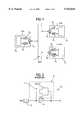
- FIG. 1shows a bus 1 connected to a number of integrated circuits 2.
- Each deviceincludes an i/o interface comprising an input buffer 3 and an output buffer 4 connected to the bus 1 via a pad 5.
- the bus 1has a low logic level of around 0 volts but a high logic level of between 3.3 and 5 volts, depending on which device is active. Only one of the devices 2 can drive the bus at any one time whilst the others are held in a high impedance state to ensure that they do not alter the logic level appearing on the bus 1. It is important that any device 2 which operates at the lower voltage level must be able to connect to the bus 1, even when the bus is at the higher voltage level.
- FIG. 2shows an input buffer 3 which includes a conventional bus hold circuit 6.
- a bus hold circuitis designed to prevent a bus from floating to an undefined state when all of the devices connected to the bus are in a high impedance state. Without this, the input buffers of devices connected to the bus could produce false transitions and may also dissipate unacceptably high currents.
- the bus hold circuit 6comprises a first CMOS inverter 7 connected in a feedback path around a second CMOS inverter 8. An input to the second CMOS inverter 8 is connected to an input pad 5.
- the first CMOS inverter 7includes a PMOS transistor connected in series with an NMOS transistor, the source of the PMOS transistor being connected to a 3.3 volt supply (Vcc).
- the input pad 5is driven by a bus and therefore the voltage which appears at the pad 5 will correspond to whatever voltage level is on the bus.
- the bus hold circuit 6is designed to allow the bus to drive the input to the second inverter 8 high or low.
- the bus hold circuit 6will hold the input at whatever logic level the bus was at until the pad 5 is next driven low or high by the bus so that the bus state does not become undefined.
- the first CMOS inverter 7To sustain a bus hold, the first CMOS inverter 7 must be connected to the pad 5.
- a parasitic N-well diode(not shown) associated with the PMOS transistor of the first CMOS inverter 7 becomes forward biassed and injects current into Vcc.
- the N-well diodeturns on when the pad voltage rises above Vcc.
- the PMOS transistorturns on as its drain voltage rises above Vcc causing an additional drain-source current to flow.
- the effect of the overvoltage on pad 5is to source current from a device driving the pad into Vcc. This will lead to a low transition on the bus and may even damage the device driving the bus to 5 volts.
- the bus hold circuit 6 shown in FIG. 2cannot be connected to a mixed bus of the type shown in FIG. 1 because the PMOS transistor components will not function properly.
- an NMOS transistoris used instead of a PMOS transistor in inverter 7 the problem of current injection into the 3.3 volt apply under overvoltage conditions could be avoided.
- an NMOS transistor connected to Vccdoes produce a sufficiently high voltage level on its output due to its threshold voltage and backbody effects.
- An NMOS transistorcould be used if its gate voltage is raised to a voltage higher than the on-chip supply Vcc by an amount which would overcome the threshold and backbody effects.
- FIG. 3shows a simplified example of a conventional output buffer 9 which includes a number of CMOS inverters which use PMOS transistors powered by a 3.3 volt supply (Vcc).
- Vcc3.3 volt supply
- an overvoltage tolerant interface for a semiconductor integrated devicecomprising:
- an isolation switchoperative to isolate the pull-up transistor from the voltage supply when a voltage at the pad exceeds the operating voltage of the voltage supply.
- the overvoltage tolerant interfacefurther comprises a voltage reference circuit coupled to the pad, configured to generate a reference voltage which tracks the voltage at the pad in a predetermined manner when the pad voltage exceeds the operating voltage of the voltage supply.
- the pull-up transistor and isolation switchare configured as components of a bus hold circuit of an input buffer.
- the pull-up transistor and isolation switchare configured as components of a pre-driver circuit of an output buffer.
- the isolation switch and the pull-up transistorare PMOS transistors.
- a mixed voltage bus systemcomprises a number of semiconductor integrated devices, at least one of which includes an overvoltage tolerant interface circuit in accordance with the first aspect of the present invention.
- a method of protecting a semiconductor integrated device from an overvoltagecomprising the step of applying a voltage reference to a switch to open the switch when the voltage at a pad of the device exceeds the operating voltage of a voltage supply and thereby electronically isolate a pull-up transistor connected to said pad from a voltage supply of the device wherein the switch is coupled between the pull-up transistor and the voltage supply.
- the isolation of the pull-up transistoris affected by controlling the operational state of an isolation switch coupled between the pull-up transistor and the voltage supply.
- the present inventionprovides i/o buffers which include PMOS components which are overvoltage-tolerant and can therefore be connected to a mixed voltage bus whilst retaining their functionality and without affecting the performance of the bus.
- FIG. 1shows a mixed voltage bus
- FIG. 2shows a conventional input buffer having a bus hold circuit
- FIG. 3shows a conventional output buffer
- FIG. 4is a block diagram showing an overvoltage tolerant input/output interface in accordance with the present invention.
- FIG. 5shows an example of an overvoltage tolerant input buffer having a bus hold circuit in accordance with the present invention
- FIG. 6shows a voltage reference signal used to control the input buffer of FIG. 5;
- FIG. 7shows an N-well bias signal used to control the input buffer of FIG. 5;
- FIG. 8shows an example of a reference voltage generating circuit in accordance with the present invention for generating the voltage reference signal shown in FIG. 6;
- FIG. 9shows an N-well bias signal generating circuit
- FIG. 10shows a detailed circuit for an input buffer
- FIG. 11shows an example of an overvoltage tolerant output buffer in accordance with the present invention.
- FIG. 4is a block diagram of an example of an overvoltage tolerant i/o interface 10 for an integrated circuit in accordance with the present invention.
- the i/o interface 10comprises an input buffer 11 having a bus hold circuit 12 and an output buffer 13, each of which is connected to a common pad 14.
- a reference voltage generating circuit 15 and an N-well bias signal generating circuit 16are also connected to the pad 14 and, as will be described below, control the operation of the input buffer 11 and the output buffer 13.
- the signals V ref and NSUB generated by each of these circuits, respectively,are coupled to the gates and N-wells, respectively, of a number of PMOS transistor components found within the input buffer 11 and the output buffer 13 to provide an overvoltage tolerant interface suitable for connection to a mixed voltage bus (not shown).
- each of these signalsis arranged to track whatever voltage appears at the pad 14 in a predetermined manner.
- FIG. 5shows an input buffer with bus hold circuit 12 in more detail.
- the bus hold circuit 12 of the present inventionincludes an isolation transistor 17 in the form of a first PMOS transistor coupled between the source of a second PMOS transistor 18 and the supply voltage Vcc.
- the gate of the isolation transistor 17is controlled by the reference voltage signal V ref whilst the N-wells of each of the PMOS transistors of the bus hold circuit are controlled by the N-well bias signal NSUB.
- voltage reference signal V refremains at zero provided the voltage at the pad 14 does not exceed Vcc. Under these conditions, the isolation transistor 17 remains on and therefore the bus hold circuit 12 functions in the conventional manner. However, if the pad voltage rises above Vcc, the voltage reference V ref then tracks the pad voltage to control the voltage at the gate of the isolation transistor 17. This causes the isolation transistor 17 to turn off, thereby isolating the second PMOS transistor 18 from the voltage source Vcc. Accordingly, although the drain voltage of the second PMOS transistor 18 may rise well above Vcc, the transistor 18 does not source current to Vcc.
- the N-well bias signal NSUBis held constant at a level substantially equal to Vcc providing the pad voltage is below Vcc. If the pad, voltage rises above Vcc, the N-well bias signal NSUB then tracks the pad voltage. This ensures that the parasitic N-well diodes in the PMOS transistor components 17 and 18 of the bus hold circuit remain reverse biassed and therefore do not source current to Vcc.
- the voltage reference signal V refis supplied by the voltage reference signal generating circuit 15 shown in detail in FIG. 8. This circuit is designed to detect when the voltage at the pad 14 exceeds Vcc and then feed the overvoltage input onto the gate of the isolation transistor 17 shown in FIG. 5. This ensures that the gate-source voltage (Vgs) is zero and so prevents the isolation transistor 17 from turning on.
- the voltage reference generating circuit 15 of FIG. 8comprises a concatenated series of inverters I1 to I3. each comprising a PMOS transistor connected in series with an NMOS transistor.
- the N-wells of each of the PMOS transistorsare driven by the N-well bias signal (NSUB) described above to ensure that the parasitic N-well diodes remain reverse biassed and therefore do not source current to Vcc.
- the sources of each of the PMOS transistors of the inverters I1 to I3are connected to the pad 14.
- the gates of the transistors in a first inverter I1are tied to the voltage source Vcc.
- An output of the first inverter I2is fed via a further inverter I4 in a feed forward circuit path 19 to an NMOS pull-down transistor 20 at the output of the circuit.
- the PMOS transistor in the first inverter I1turns off and the associated NMOS transistor turns on. This gives a low output at node N1 which, once inverted by inverter I4, causes NMOS transistor 20 to turn on, pulling the output at node N2 of the circuit low.
- the PMOS transistor in the first inverter I1turns on so that the output at node N1 is pulled up to the voltage of the pad 14. This voltage is then passed through the following inverter stages I2 and I3 and appears at Node N2 at the output of the circuit. Accordingly, as shown in FIG. 6, when the pad voltage rises above Vcc, the voltage reference V ref tracks the pad voltage.
- the concatenated series of inverters I1 to I3act as buffers and so improve the edge rate of the V ref signal.
- the PMOS transistor in inverter I1is significantly larger, and hence more powerful, than the corresponding NMOS transistor. Accordingly, when the PMOS transistor turns on it is able to pull node N1 high despite the efforts of the NMOS transistor to pull this node low.
- the concatenation of the buffers I1 to I3is required to decouple the large load capacitance connected on node N2 from the output of the inverter I1.
- FIG. 9shows an N-well bias signal NSUB generating circuit 16.
- This circuitis conventional. As shown, the circuit comprises a pair of PMOS transistors 21 and 22 connected in series between a supply rail Vcc and the pad 14. The gate of PMOS transistor 21 is connected to the pad 14 and so is controlled in dependence on whatever voltage appears at the pad 14, whilst the gate of PMOS transistor 22 is connected to Vcc. As described above with respect to FIG. 7, when the pad voltage is below Vcc, the output of the NSUB circuit 16 is held constant at a voltage level substantially equal to Vcc. Should the pad voltage rise above Vcc, the output NSUB tracks the pad voltage.
- the NSUB output signalis fed to a number of PMOS transistor components in the i/o interface 10 to bias the N-wells. This keeps the parasitic diodes of the N-wells reverse biassed so they do not source current to the supply voltage Vcc of the associated device.
- FIG. 10is a detailed circuit for an input buffer for an integrated circuit which implements a bus hold function, showing the bus hold circuit 12, voltage reference generating circuit 15 and NSUB generating circuit 16 described above connected together. As shown, the voltage reference generating circuit also generates a signal V ref B. Under normal conditions this signal is at a voltage level substantially equal to the supply voltage Vcc. In an overvoltage state V ref B corresponds to the level of Vss.
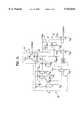
- FIG. 11shows an example of an overvoltage tolerant output buffer in accordance with the present invention.
- the voltage reference generating circuit and N-well bias signal generating circuithave been omitted for clarity.
- the N-wells of the PMOS transistor components in the circuitare connected to the N-well bias signal NSUB.
- the output bufferincludes a pre-driver circuit 23, a PMOS transistor 24 and an NMOS transistor 25.
- the voltage reference signal V ref Bis connected to the gate of a PMOS transistor 26.
- the source of the transistor 26is connected to the gate of an output PMOS transistor 27 and the drain is connected to the pad 14. Under overvoltage conditions, transistor 26 turns on and so raises the gate voltage of transistor 27 to that of the pad 14.
- Two isolation transistors 28 and 29are provided in the pre-driver 23.
- PMOS isolation transistor 28prevents current injection into Vcc because its gate is connected to V ref
- NMOS isolation transistor 29prevents leakage into Vss because its gate is coupled to V ref B which ensures that the
- the i/o buffers described aboveare overvoltage tolerant and can therefore be connected to a mixed voltage bus whilst retaining their functionality and without affecting the performance of the bus.
Landscapes
- Physics & Mathematics (AREA)
- Engineering & Computer Science (AREA)
- Computer Hardware Design (AREA)
- Computing Systems (AREA)
- General Engineering & Computer Science (AREA)
- Mathematical Physics (AREA)
- Logic Circuits (AREA)
Abstract
Description
Claims (14)
Priority Applications (1)
| Application Number | Priority Date | Filing Date | Title |
|---|---|---|---|
| US08/949,863US5914844A (en) | 1997-10-14 | 1997-10-14 | Overvoltage-tolerant input-output buffers having a switch configured to isolate a pull up transistor from a voltage supply |
Applications Claiming Priority (1)
| Application Number | Priority Date | Filing Date | Title |
|---|---|---|---|
| US08/949,863US5914844A (en) | 1997-10-14 | 1997-10-14 | Overvoltage-tolerant input-output buffers having a switch configured to isolate a pull up transistor from a voltage supply |
Publications (1)
| Publication Number | Publication Date |
|---|---|
| US5914844Atrue US5914844A (en) | 1999-06-22 |
Family
ID=25489604
Family Applications (1)
| Application Number | Title | Priority Date | Filing Date |
|---|---|---|---|
| US08/949,863Expired - LifetimeUS5914844A (en) | 1997-10-14 | 1997-10-14 | Overvoltage-tolerant input-output buffers having a switch configured to isolate a pull up transistor from a voltage supply |
Country Status (1)
| Country | Link |
|---|---|
| US (1) | US5914844A (en) |
Cited By (20)
| Publication number | Priority date | Publication date | Assignee | Title |
|---|---|---|---|---|
| US6150845A (en)* | 1999-06-01 | 2000-11-21 | Fairchild Semiconductor Corp. | Bus hold circuit with overvoltage tolerance |
| US6184715B1 (en)* | 1997-11-14 | 2001-02-06 | Stmicroelectronics S.R.L. | Bus-hold input circuit adapted for receiving input signals with voltage levels higher than the voltage supply thereof |
| US6236236B1 (en)* | 1999-06-02 | 2001-05-22 | National Semiconductor Corporation | 2.5 volt input/output buffer circuit tolerant to 3.3 and 5 volts |
| US6252375B1 (en)* | 2000-07-24 | 2001-06-26 | In-System Design, Inc. | Power management system and current augmentation and battery charger method and apparatus for a computer peripheral |
| US6265931B1 (en)* | 1997-10-14 | 2001-07-24 | Cypress Semiconductor Corp. | Voltage reference source for an overvoltage-tolerant bus interface |
| US20020078389A1 (en)* | 2000-12-20 | 2002-06-20 | Xiaolin Yuan | Apparatus and method for a low power, multi-level GTL I/O buffer with fast restoration of static bias |
| US6496054B1 (en) | 2000-05-13 | 2002-12-17 | Cypress Semiconductor Corp. | Control signal generator for an overvoltage-tolerant interface circuit on a low voltage process |
| US20030040278A1 (en)* | 2001-08-22 | 2003-02-27 | Iliadis Agisilaos A. | System and method for protecting devices from interference signals |
| US6538867B1 (en)* | 2000-11-15 | 2003-03-25 | Fairchild Semiconductor Corporation | FET switch with overvoltage protection |
| US6577163B1 (en) | 2000-12-21 | 2003-06-10 | Cypress Semiconductor Corp. | Configurable PCI clamp or high voltage tolerant I/O circuit |
| US20030151428A1 (en)* | 2002-02-12 | 2003-08-14 | Ouyang Paul H. | 5 Volt tolerant input/output buffer |
| US20040183567A1 (en)* | 2003-03-20 | 2004-09-23 | Engler David W. | Isolated channel in an integrated circuit |
| US20060181315A1 (en)* | 2005-02-12 | 2006-08-17 | Samsung Electronics Co., Ltd. | Bus holders having wide input and output voltage ranges and tolerant input/output buffers using the same |
| US7202699B1 (en) | 2003-09-15 | 2007-04-10 | Cypress Semiconductor Corporation | Voltage tolerant input buffer |
| US7321238B1 (en) | 2005-12-22 | 2008-01-22 | Integrated Device Technology, Inc. | Over-voltage tolerant multifunction input stage |
| US20080150577A1 (en)* | 2003-06-30 | 2008-06-26 | Tatsuya Ueno | Interface Circuit |
| US7394293B1 (en) | 2003-09-25 | 2008-07-01 | Cypress Semiconductor Corp. | Circuit and method for rapid power up of a differential output driver |
| US7408751B1 (en)* | 2005-09-15 | 2008-08-05 | Integrated Device Technology, Inc. | Self-biased electrostatic discharge protection method and circuit |
| US8018268B1 (en) | 2004-11-19 | 2011-09-13 | Cypress Semiconductor Corporation | Over-voltage tolerant input circuit |
| JP2013247383A (en)* | 2012-05-23 | 2013-12-09 | Fujitsu Semiconductor Ltd | Semiconductor integrated circuit |
Citations (26)
| Publication number | Priority date | Publication date | Assignee | Title |
|---|---|---|---|---|
| US4472647A (en)* | 1982-08-20 | 1984-09-18 | Motorola, Inc. | Circuit for interfacing with both TTL and CMOS voltage levels |
| US4555642A (en)* | 1983-09-22 | 1985-11-26 | Standard Microsystems Corporation | Low power CMOS input buffer circuit |
| US4642488A (en)* | 1985-09-03 | 1987-02-10 | Codex Corporation | CMOS input buffer accepting TTL level inputs |
| US4698526A (en)* | 1985-10-17 | 1987-10-06 | Inmos Corporation | Source follower CMOS input buffer |
| US4763021A (en)* | 1987-07-06 | 1988-08-09 | Unisys Corporation | CMOS input buffer receiver circuit with ultra stable switchpoint |
| US4825415A (en)* | 1985-12-06 | 1989-04-25 | Nec Corporation | Signal input circuit having signal latch function |
| US4930112A (en)* | 1985-11-22 | 1990-05-29 | Hitachi, Ltd. | Semiconductor device having a voltage limiter |
| US4937700A (en)* | 1988-01-07 | 1990-06-26 | Kabushiki Kaisha Toshiba | Semiconductor integrated circuit with a circuit limiting an input voltage to a predetermined voltage |
| US4964084A (en)* | 1988-12-15 | 1990-10-16 | Samsung Electronics Co., Ltd. | Static random access memory device with voltage control circuit |
| US5115150A (en)* | 1990-11-19 | 1992-05-19 | Hewlett-Packard Co. | Low power CMOS bus receiver with small setup time |
| US5117177A (en)* | 1991-01-23 | 1992-05-26 | Ramtron Corporation | Reference generator for an integrated circuit |
| US5144167A (en)* | 1991-05-10 | 1992-09-01 | Altera Corporation | Zero power, high impedance TTL-to-CMOS converter |
| US5247212A (en)* | 1991-01-31 | 1993-09-21 | Thunderbird Technologies, Inc. | Complementary logic input parallel (clip) logic circuit family |
| US5268599A (en)* | 1990-09-27 | 1993-12-07 | Kabushiki Kaisha Toshiba | TTL to CMOS input buffer using CMOS structure |
| US5300832A (en)* | 1992-11-10 | 1994-04-05 | Sun Microsystems, Inc. | Voltage interfacing buffer with isolation transistors used for overvoltage protection |
| US5329184A (en)* | 1992-11-05 | 1994-07-12 | National Semiconductor Corporation | Method and apparatus for feedback control of I/O characteristics of digital interface circuits |
| US5359243A (en)* | 1993-04-16 | 1994-10-25 | Altera Corporation | Fast TTL to CMOS level converting buffer with low standby power |
| US5359240A (en)* | 1993-01-25 | 1994-10-25 | National Semiconductor Corporation | Low power digital signal buffer circuit |
| US5406139A (en)* | 1993-03-19 | 1995-04-11 | Advanced Micro Devices, Inc. | Input buffer utilizing a cascode to provide a zero power TTL to CMOS input with high speed switching |
| US5455532A (en)* | 1993-04-21 | 1995-10-03 | Texas Instruments Incorporated | 3V to 5V receiver/translator using a 5V supply and a 3V reference |
| US5455527A (en)* | 1992-09-18 | 1995-10-03 | Siemens Aktiengesellschaft | CMOS buffer circuit with controlled current source |
| US5467031A (en)* | 1994-09-22 | 1995-11-14 | Lsi Logic Corporation | 3.3 volt CMOS tri-state driver circuit capable of driving common 5 volt line |
| US5510738A (en)* | 1995-03-01 | 1996-04-23 | Lattice Semiconductor Crop. | CMOS programmable resistor-based transconductor |
| US5555149A (en)* | 1993-06-07 | 1996-09-10 | National Semiconductor Corporation | Overvoltage protection |
| US5570043A (en)* | 1995-01-31 | 1996-10-29 | Cypress Semiconductor Corporation | Overvoltage tolerant intergrated circuit output buffer |
| US5576635A (en)* | 1995-02-14 | 1996-11-19 | Advanced Micro Devices, Inc. | Output buffer with improved tolerance to overvoltage |
- 1997
- 1997-10-14USUS08/949,863patent/US5914844A/ennot_activeExpired - Lifetime
Patent Citations (27)
| Publication number | Priority date | Publication date | Assignee | Title |
|---|---|---|---|---|
| US4472647A (en)* | 1982-08-20 | 1984-09-18 | Motorola, Inc. | Circuit for interfacing with both TTL and CMOS voltage levels |
| US4555642A (en)* | 1983-09-22 | 1985-11-26 | Standard Microsystems Corporation | Low power CMOS input buffer circuit |
| US4642488A (en)* | 1985-09-03 | 1987-02-10 | Codex Corporation | CMOS input buffer accepting TTL level inputs |
| US4698526A (en)* | 1985-10-17 | 1987-10-06 | Inmos Corporation | Source follower CMOS input buffer |
| US4930112A (en)* | 1985-11-22 | 1990-05-29 | Hitachi, Ltd. | Semiconductor device having a voltage limiter |
| US4825415A (en)* | 1985-12-06 | 1989-04-25 | Nec Corporation | Signal input circuit having signal latch function |
| US4763021A (en)* | 1987-07-06 | 1988-08-09 | Unisys Corporation | CMOS input buffer receiver circuit with ultra stable switchpoint |
| US4937700A (en)* | 1988-01-07 | 1990-06-26 | Kabushiki Kaisha Toshiba | Semiconductor integrated circuit with a circuit limiting an input voltage to a predetermined voltage |
| US4964084A (en)* | 1988-12-15 | 1990-10-16 | Samsung Electronics Co., Ltd. | Static random access memory device with voltage control circuit |
| US5268599A (en)* | 1990-09-27 | 1993-12-07 | Kabushiki Kaisha Toshiba | TTL to CMOS input buffer using CMOS structure |
| US5115150A (en)* | 1990-11-19 | 1992-05-19 | Hewlett-Packard Co. | Low power CMOS bus receiver with small setup time |
| US5117177A (en)* | 1991-01-23 | 1992-05-26 | Ramtron Corporation | Reference generator for an integrated circuit |
| US5247212A (en)* | 1991-01-31 | 1993-09-21 | Thunderbird Technologies, Inc. | Complementary logic input parallel (clip) logic circuit family |
| US5144167A (en)* | 1991-05-10 | 1992-09-01 | Altera Corporation | Zero power, high impedance TTL-to-CMOS converter |
| US5455527A (en)* | 1992-09-18 | 1995-10-03 | Siemens Aktiengesellschaft | CMOS buffer circuit with controlled current source |
| US5329184A (en)* | 1992-11-05 | 1994-07-12 | National Semiconductor Corporation | Method and apparatus for feedback control of I/O characteristics of digital interface circuits |
| US5300832A (en)* | 1992-11-10 | 1994-04-05 | Sun Microsystems, Inc. | Voltage interfacing buffer with isolation transistors used for overvoltage protection |
| US5359240A (en)* | 1993-01-25 | 1994-10-25 | National Semiconductor Corporation | Low power digital signal buffer circuit |
| US5406139A (en)* | 1993-03-19 | 1995-04-11 | Advanced Micro Devices, Inc. | Input buffer utilizing a cascode to provide a zero power TTL to CMOS input with high speed switching |
| US5359243A (en)* | 1993-04-16 | 1994-10-25 | Altera Corporation | Fast TTL to CMOS level converting buffer with low standby power |
| US5455532A (en)* | 1993-04-21 | 1995-10-03 | Texas Instruments Incorporated | 3V to 5V receiver/translator using a 5V supply and a 3V reference |
| US5555149A (en)* | 1993-06-07 | 1996-09-10 | National Semiconductor Corporation | Overvoltage protection |
| US5467031A (en)* | 1994-09-22 | 1995-11-14 | Lsi Logic Corporation | 3.3 volt CMOS tri-state driver circuit capable of driving common 5 volt line |
| US5570043A (en)* | 1995-01-31 | 1996-10-29 | Cypress Semiconductor Corporation | Overvoltage tolerant intergrated circuit output buffer |
| US5576635A (en)* | 1995-02-14 | 1996-11-19 | Advanced Micro Devices, Inc. | Output buffer with improved tolerance to overvoltage |
| US5510738A (en)* | 1995-03-01 | 1996-04-23 | Lattice Semiconductor Crop. | CMOS programmable resistor-based transconductor |
| US5574678A (en)* | 1995-03-01 | 1996-11-12 | Lattice Semiconductor Corp. | Continuous time programmable analog block architecture |
Non-Patent Citations (7)
| Title |
|---|
| Daniel W. Dobberpuhl, et al., A 200 MHz 64 b Dual Issue CMOS Microprocessor, Nov., 1992, IEEE Journal of Solid State Circuits, vol. 27, No. 11.* |
| Daniel W. Dobberpuhl, et al., A 200-MHz 64-b Dual-Issue CMOS Microprocessor, Nov., 1992, IEEE Journal of Solid-State Circuits, vol. 27, No. 11. |
| Makoto Ueda, et al., A 3.3V ASIC for Mixed Voltage Applications with Shut Down Mode, 1993, IEEE Custom Integrated Circuits Conference.* |
| Marcel J. M. Pelgrom, et al., A 3/5 V Compatible I/O Buffer, Jul. 1995, IEEE Journal of Solid State Circuits, vol. 30, No. 7.* |
| Marcel J. M. Pelgrom, et al., A 3/5 V Compatible I/O Buffer, Jul. 1995, IEEE Journal of Solid-State Circuits, vol. 30, No. 7. |
| Rakesh Patel, et al., A 3.3 V Programmable Logic Device that Addresses Low Power Supply and Interface Trends, 1997, IEEE Custom Integrated Circuits Conference.* |
| Rakesh Patel, et al., A 3.3-V Programmable Logic Device that Addresses Low Power Supply and Interface Trends, 1997, IEEE Custom Integrated Circuits Conference. |
Cited By (29)
| Publication number | Priority date | Publication date | Assignee | Title |
|---|---|---|---|---|
| US6265931B1 (en)* | 1997-10-14 | 2001-07-24 | Cypress Semiconductor Corp. | Voltage reference source for an overvoltage-tolerant bus interface |
| US6184715B1 (en)* | 1997-11-14 | 2001-02-06 | Stmicroelectronics S.R.L. | Bus-hold input circuit adapted for receiving input signals with voltage levels higher than the voltage supply thereof |
| US6150845A (en)* | 1999-06-01 | 2000-11-21 | Fairchild Semiconductor Corp. | Bus hold circuit with overvoltage tolerance |
| US6236236B1 (en)* | 1999-06-02 | 2001-05-22 | National Semiconductor Corporation | 2.5 volt input/output buffer circuit tolerant to 3.3 and 5 volts |
| US6496054B1 (en) | 2000-05-13 | 2002-12-17 | Cypress Semiconductor Corp. | Control signal generator for an overvoltage-tolerant interface circuit on a low voltage process |
| US6252375B1 (en)* | 2000-07-24 | 2001-06-26 | In-System Design, Inc. | Power management system and current augmentation and battery charger method and apparatus for a computer peripheral |
| US6538867B1 (en)* | 2000-11-15 | 2003-03-25 | Fairchild Semiconductor Corporation | FET switch with overvoltage protection |
| US20020078389A1 (en)* | 2000-12-20 | 2002-06-20 | Xiaolin Yuan | Apparatus and method for a low power, multi-level GTL I/O buffer with fast restoration of static bias |
| US6785828B2 (en)* | 2000-12-20 | 2004-08-31 | Intel Corporation | Apparatus and method for a low power, multi-level GTL I/O buffer with fast restoration of static bias |
| US6577163B1 (en) | 2000-12-21 | 2003-06-10 | Cypress Semiconductor Corp. | Configurable PCI clamp or high voltage tolerant I/O circuit |
| US20030040278A1 (en)* | 2001-08-22 | 2003-02-27 | Iliadis Agisilaos A. | System and method for protecting devices from interference signals |
| US6968157B2 (en) | 2001-08-22 | 2005-11-22 | University Of Maryland | System and method for protecting devices from interference signals |
| US20030151428A1 (en)* | 2002-02-12 | 2003-08-14 | Ouyang Paul H. | 5 Volt tolerant input/output buffer |
| US6975136B2 (en)* | 2003-03-20 | 2005-12-13 | Hewlett-Packard Development Company, L.P. | Isolated channel in an integrated circuit |
| US20040183567A1 (en)* | 2003-03-20 | 2004-09-23 | Engler David W. | Isolated channel in an integrated circuit |
| US8018264B2 (en)* | 2003-06-30 | 2011-09-13 | Yamatake Corporation | Interface circuit |
| US20080150577A1 (en)* | 2003-06-30 | 2008-06-26 | Tatsuya Ueno | Interface Circuit |
| US7750705B2 (en)* | 2003-06-30 | 2010-07-06 | Yamatake Corporation | Interface circuit |
| US20110133775A1 (en)* | 2003-06-30 | 2011-06-09 | Yamatake Corporation | Interface circuit |
| US20110133779A1 (en)* | 2003-06-30 | 2011-06-09 | Yamatake Corporation | Interface circuit |
| US7986162B2 (en)* | 2003-06-30 | 2011-07-26 | Yamatake Corporation | Interface circuit |
| US7202699B1 (en) | 2003-09-15 | 2007-04-10 | Cypress Semiconductor Corporation | Voltage tolerant input buffer |
| US7394293B1 (en) | 2003-09-25 | 2008-07-01 | Cypress Semiconductor Corp. | Circuit and method for rapid power up of a differential output driver |
| US8018268B1 (en) | 2004-11-19 | 2011-09-13 | Cypress Semiconductor Corporation | Over-voltage tolerant input circuit |
| US20060181315A1 (en)* | 2005-02-12 | 2006-08-17 | Samsung Electronics Co., Ltd. | Bus holders having wide input and output voltage ranges and tolerant input/output buffers using the same |
| US7504867B2 (en) | 2005-02-12 | 2009-03-17 | Samsung Electronics Co., Ltd. | Bus holders having wide input and output voltage ranges and tolerant input/output buffers using the same |
| US7408751B1 (en)* | 2005-09-15 | 2008-08-05 | Integrated Device Technology, Inc. | Self-biased electrostatic discharge protection method and circuit |
| US7321238B1 (en) | 2005-12-22 | 2008-01-22 | Integrated Device Technology, Inc. | Over-voltage tolerant multifunction input stage |
| JP2013247383A (en)* | 2012-05-23 | 2013-12-09 | Fujitsu Semiconductor Ltd | Semiconductor integrated circuit |
Similar Documents
| Publication | Publication Date | Title |
|---|---|---|
| US5914844A (en) | Overvoltage-tolerant input-output buffers having a switch configured to isolate a pull up transistor from a voltage supply | |
| US5933025A (en) | Low voltage interface circuit with a high voltage tolerance | |
| US5534795A (en) | Voltage translation and overvoltage protection | |
| EP0614279B1 (en) | Overvoltage tolerant output buffer circuit | |
| EP0608489B1 (en) | Low-to-high voltage translator with latch-up immunity | |
| US5828262A (en) | Ultra low power pumped n-channel output buffer with self-bootstrap | |
| EP0621692B1 (en) | Overvoltage protection circuitry | |
| US5721508A (en) | 5 Volt tolerant 3.3 volt output buffer | |
| KR20180040958A (en) | High voltage output driver with low voltage device | |
| US6049242A (en) | Voltage reference source for an overvoltage-tolerant bus interface | |
| US7477075B2 (en) | CMOS output driver using floating wells to prevent leakage current | |
| US6313672B1 (en) | Over-voltage tolerant integrated circuit I/O buffer | |
| US6335637B1 (en) | Two-supply protection circuit | |
| US6184700B1 (en) | Fail safe buffer capable of operating with a mixed voltage core | |
| US6232818B1 (en) | Voltage translator | |
| US6580291B1 (en) | High voltage output buffer using low voltage transistors | |
| US6201428B1 (en) | 5-volt tolerant 3-volt drive push-pull buffer/driver | |
| US6294943B1 (en) | Method of designing fail-safe CMOS I/O buffers whose external nodes accept voltages higher than the maximum gate oxide operating voltage | |
| US6496054B1 (en) | Control signal generator for an overvoltage-tolerant interface circuit on a low voltage process | |
| EP0874462B1 (en) | Pull-up circuit and semiconductor device using the same | |
| US20050127953A1 (en) | 5 Volt tolerant IO scheme using low-voltage devices | |
| US6043680A (en) | 5V tolerant I/O buffer | |
| US6169432B1 (en) | High voltage switch for providing voltages higher than 2.5 volts with transistors made using a 2.5 volt process | |
| US6222387B1 (en) | Overvoltage tolerant integrated circuit input/output interface | |
| US6351157B1 (en) | Output buffer for making a high voltage (5.0 volt) compatible input/output in a low voltage (2.5 volt) semiconductor process |
Legal Events
| Date | Code | Title | Description |
|---|---|---|---|
| AS | Assignment | Owner name:CYPRESS SEMICONDUCTOR CORPORATION, CALIFORNIA Free format text:ASSIGNMENT OF ASSIGNORS INTEREST;ASSIGNORS:LUTLEY, JAMES;PANT, SANDEEP;REEL/FRAME:008782/0826 Effective date:19971010 | |
| STCF | Information on status: patent grant | Free format text:PATENTED CASE | |
| FPAY | Fee payment | Year of fee payment:4 | |
| FPAY | Fee payment | Year of fee payment:8 | |
| REMI | Maintenance fee reminder mailed | ||
| FPAY | Fee payment | Year of fee payment:12 | |
| SULP | Surcharge for late payment | Year of fee payment:11 | |
| AS | Assignment | Owner name:MORGAN STANLEY SENIOR FUNDING, INC., NEW YORK Free format text:SECURITY INTEREST;ASSIGNORS:CYPRESS SEMICONDUCTOR CORPORATION;SPANSION LLC;REEL/FRAME:035240/0429 Effective date:20150312 | |
| AS | Assignment | Owner name:CYPRESS SEMICONDUCTOR CORPORATION, CALIFORNIA Free format text:PARTIAL RELEASE OF SECURITY INTEREST IN PATENTS;ASSIGNOR:MORGAN STANLEY SENIOR FUNDING, INC., AS COLLATERAL AGENT;REEL/FRAME:039708/0001 Effective date:20160811 Owner name:SPANSION LLC, CALIFORNIA Free format text:PARTIAL RELEASE OF SECURITY INTEREST IN PATENTS;ASSIGNOR:MORGAN STANLEY SENIOR FUNDING, INC., AS COLLATERAL AGENT;REEL/FRAME:039708/0001 Effective date:20160811 | |
| AS | Assignment | Owner name:MONTEREY RESEARCH, LLC, CALIFORNIA Free format text:ASSIGNMENT OF ASSIGNORS INTEREST;ASSIGNOR:CYPRESS SEMICONDUCTOR CORPORATION;REEL/FRAME:040911/0238 Effective date:20160811 | |
| AS | Assignment | Owner name:MORGAN STANLEY SENIOR FUNDING, INC., NEW YORK Free format text:CORRECTIVE ASSIGNMENT TO CORRECT THE 8647899 PREVIOUSLY RECORDED ON REEL 035240 FRAME 0429. ASSIGNOR(S) HEREBY CONFIRMS THE SECURITY INTERST;ASSIGNORS:CYPRESS SEMICONDUCTOR CORPORATION;SPANSION LLC;REEL/FRAME:058002/0470 Effective date:20150312 |