US5913020A - Method for using fuse identification codes for masking bad bits on single in-line memory modules - Google Patents
Method for using fuse identification codes for masking bad bits on single in-line memory modulesDownload PDFInfo
- Publication number
- US5913020A US5913020AUS08/918,604US91860497AUS5913020AUS 5913020 AUS5913020 AUS 5913020AUS 91860497 AUS91860497 AUS 91860497AUS 5913020 AUS5913020 AUS 5913020A
- Authority
- US
- United States
- Prior art keywords
- memory
- circuit board
- storage device
- fail map
- identification code
- Prior art date
- Legal status (The legal status is an assumption and is not a legal conclusion. Google has not performed a legal analysis and makes no representation as to the accuracy of the status listed.)
- Expired - Lifetime
Links
Images


Classifications
- G—PHYSICS
- G11—INFORMATION STORAGE
- G11C—STATIC STORES
- G11C29/00—Checking stores for correct operation ; Subsequent repair; Testing stores during standby or offline operation
- G11C29/70—Masking faults in memories by using spares or by reconfiguring
- G11C29/72—Masking faults in memories by using spares or by reconfiguring with optimized replacement algorithms
- G—PHYSICS
- G11—INFORMATION STORAGE
- G11C—STATIC STORES
- G11C29/00—Checking stores for correct operation ; Subsequent repair; Testing stores during standby or offline operation
- G11C29/04—Detection or location of defective memory elements, e.g. cell constructio details, timing of test signals
- G11C29/08—Functional testing, e.g. testing during refresh, power-on self testing [POST] or distributed testing
- G11C29/12—Built-in arrangements for testing, e.g. built-in self testing [BIST] or interconnection details
- G11C2029/1208—Error catch memory
- H—ELECTRICITY
- H01—ELECTRIC ELEMENTS
- H01L—SEMICONDUCTOR DEVICES NOT COVERED BY CLASS H10
- H01L2223/00—Details relating to semiconductor or other solid state devices covered by the group H01L23/00
- H01L2223/544—Marks applied to semiconductor devices or parts
- H01L2223/54433—Marks applied to semiconductor devices or parts containing identification or tracking information
- H01L2223/5444—Marks applied to semiconductor devices or parts containing identification or tracking information for electrical read out
Definitions
- This inventionrelates generally to the field of integrated circuit manufacturing, and more particularly to a method for masking failing memory locations on a SIMM module.
- DRAMDynamic Random-Access-Memory
- SIMMSingle In-Line Memory Module
- DRAMsare sometimes manufactured with a failing memory location. It is desirable not to throw away DRAMs with failing memory locations because this results in a loss of revenue. Instead, DRAMs with failing memory locations can still be incorporated onto a SIMM while still maintaining proper SIMM functionality.
- Another type of chiptypically an application specific integrated circuit (ASIC)
- ASICapplication specific integrated circuit
- Such back-up memorycan be located in the ASIC itself, or could constitute a designated portion of DRAM memory already included on the SIMM. Either way, the failing locations, by the use of the programmable ASIC, are effectively masked from the SIMM consumer, who notices no loss in functionality.
- U.S. Pat. No. 5,315,552(Yoneda) describes a basic use of this technique.
- DRAMs used in SIMM manufacturingcan be tested individually both before and after assembly onto a SIMM printed circuit board. It is usually the case that the individual DRAMs can be scrutinized for failures with greater sensitivity before assembly of the DRAMs onto the SIMM. This results because SIMM testers are generally not as sophisticated as individual chip testers, and because the electrical interference of the SIMM board and the other DRAMs present on the SIMM board, preclude an unhampered investigation of a single DRAM once it is assembled onto a SIMM. For this reason, it is desirable to use the data gathered while testing the DRAMs before SIMM assembly to assist in programming the ASIC to mask the failing locations.
- DRAMsBefore SIMM assembly, DRAMs may be tested under a variety of conditions to try and aggravate potentially latent failures. For example, a DRAM could be tested at cold (-10 Centigrade) or high (+85 Centigrade) temperatures, or subject to various timing conditions, or subject to different voltage conditions, etc.
- a "fail map” of the devicecan be generated.
- a “fail map”is constructed by writing a pre-selected pattern into a DRAM, and then reading out the pattern. If the DRAM is working properly, then the pattern written into the DRAM and the pattern read out of the DRAM, when compared, should be the same. If there are no differences, the fail map will be blank. But if a difference exists between the two patterns, for example, if a "1" is written into a particular memory location, but a "0" is read, or vice versa, then the device has a failure at the given memory location. The failing memory location (or locations) is logged into the fail map.
- the fail maps for a given deviceare stored by means of a computer which is connected to the memory tester which generated the fail map.
- Testing the device under various conditionsis desirable because some modes of failure may be present only when subjected to a particular test condition (e.g., a given memory location may only fail at high temperature, or when subjected to lower than usual voltages, etc.).
- a particular test conditione.g., a given memory location may only fail at high temperature, or when subjected to lower than usual voltages, etc.
- several different fail mapscan be generated, which may or may not be equivalent. From these fail maps, a "worst case fail map" can be generated which contains all failing locations (generated from any of the test conditions) in a single map.
- the programming of the ASIC to mask out failing memory locationsis inefficient.
- the SIMM itselfis tested to determine if there are any failing memory locations. If failing locations are detected, the fail maps of the DRAMs which were generated before SIMM assembly are searched to see if a "match" can be located. In other words, the fail maps of an individual DRAM are read off of the SIMM and are compared to the hosts of files that were collected from the individual DRAMs pre-SIMM assembly. Typically, this process of matching compares the SIMM data to the worst case fail map generated before SIMM assembly.
- the individual DRAM fail mapsare generally much more sensitive and therefore provide the most conservative summary of which failing locations should be masked off to maximize product reliability.
- the pre-assembly datamay be relied on, instead of the SIMM data, when programming the ASIC.
- the matching processcan be both time consuming and inaccurate. It is time consuming because the pattern matching process must sort through relatively large fail maps to try and locate a matching map. Also, it is inaccurate since the fails generated when the DRAMs are on a SIMM will likely only show a portion of the failures that were highlighted in the DRAM fail maps generated before SIMM assembly, therefore making pattern matching difficult.
- a new method for masking off failing memory locations on a Single In-line Memory Moduleentails reading out the identification (ID) codes which are fused in the individual DRAMs.
- ID codesare used to index stored fail maps which were taken from the DRAMs prior to their assembly onto the SIMM. After all failing locations of all of the DRAMs located on a single SIMM are determined, the SIMM is then programmed to re-route these locations to auxiliary memory located on the SIMM.
- FIG. 1shows the layout of DRAM and ASIC devices on a SIMM.
- FIG. 2shows a block diagram of one embodiment of an apparatus as may be used to implement the invention in one particular embodiment.
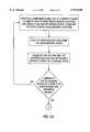
- FIG. 3illustrates one embodiment of a method of programming a circuit board including a memory device having a plurality of memory locations and a machine-readable identification code.
- FIG. 4illustrates a variation on the embodiment of FIG. 3 in which a part of the method is performed at different operating temperatures for the same memory device.
- FIG. 4Aillustrates another variation on the embodiment of FIG. 3 in which a part of the method is performed in different operating modes for the same memory device.
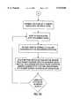
- FIGS. 5A and 5Billustrate an embodiment of a method for testing a plurality of memory devices after their assembly onto a circuit board.
- FIG 6illustrates an embodiment of a method of using a SIMM test head and a storage device.
- the methodtakes advantage of the identification (ID) code 100 that is fused into a DRAM 105, upon its manufacture, to retrieve more quickly and accurately the stored fail maps for the individual DRAMs 105 that have been assembled onto the SIMM 115, without the need for pattern matching.
- the ID code 100 for a DRAM 105is typically "burned in” to a given DRAM 105 after a DRAM wafer has finished fabrication, but before the wafer has been "diced” into individual devices suitable for assembly into packages.
- the ID code 100is typically comprised of a specialized bank of dielectric antifuses (e.g., capacitors) which exists outside of the normal array of DRAM cells 110. The antifuses are selectively destroyed to give each individual chip a unique ID code 100. Antifuses are not the only way to construct an ID code 100, of course; for example, laser fuses, sometimes used to program DRAM redundancy circuits, can also be used.
- FIG. 1also shows an ASIC device 120 which is assembled onto the SIMM 115.
- a component test head 200is configured to generate fail maps generated for the individual DRAMs 105 prior to their assembly in a SIMM.
- the design and construction of the component test head 200will depend on specific business-related constraints such as the type of memory devices to be tested but would be a matter of routine engineering for those of ordinary skill having the benefit of this disclosure.
- an individual DRAM's ID code 100is read out of the DRAM 105.
- the fail map or maps and the ID code 100are combined into a record in a database indexed by the ID code 100.
- the databasemay be simple in form, e.g., a conventional comma-delimited text file with one record per line; alternatively, the database may conform to a database management system (DBMS) format such as MICROSOFT ACCESS, DBASE, etc.
- DBMSdatabase management system
- the record for the individual DRAM 100may be stored in a computer 205 connected to the component test head 200. While the fail maps are still resident in the component test head 200 or after the fail maps have been stored in the computer 205, a worst case fail map can likewise be generated and stored, again indexed by the ID code 100.
- the computer 205need not be directly and physically linked to component test head 200.
- datacould instead be transferred from the component test head 200 by storing the data files onto a floppy disk and transferring the data by hand to the computer 205.
- a variety of storage devicescould be used in lieu of a computer 205; in addition, the component test head 200 may contain its own internal computer 205 or other storage device.
- the method for extracting the ID codes 100will vary depending on manufacture and device variations. Some DRAMs 105 might not contain ID codes 100, in which case the operations described above and in the discussion below can be selectively omitted as appropriate.
- the DRAMs 105are next sent to a conventional SIMM assembly station 210, where they are assembled onto SIMM printed circuit boards, or a similar equivalent, such as a Multi-Chip Module (MCM).
- MCMMulti-Chip Module
- the SIMM test head 215will typically comprise a processor (which may be internal 220 or may be part of the computer 205) and suitable conventional circuitry for reading an ID code 100 from DRAMs 105 and for programming replacement memory on a SIMM, e.g., the ASIC 120.
- the processormay be controlled by program instructions stored in a program storage device such as a ROM 225 or EEPROM.
- the ID codes 100 for each of the DRAMs 105 on the SIMM 115are read out from the SIMM 115.
- the ID codes 100are then used to index the data files that were previously stored in computer 205.
- the fail maps from the indexed data fileare returned to the SIMM test head 215.
- the data filescan be configured in several different ways to facilitate retrieval of the fail maps. For instance, a "look-up" table which contains the ID codes 100 could be used.
- the fail mapWhen the fail map is received at the SIMM test head, the fail map is converted into a programming signal, which, as disclosed in Yoneda '552, is used to program the ASIC 120. Then the ASIC 120 is programmed to re-route those memory locations that the fail maps reveal are failing.
- the conversion of the fail map into a programming signalcan also be performed at computer 205 and the programming signal can be sent directly to the SIMM test head 215 without the need for further processing. Furthermore, the conversion of the fail map into a programming signal will be dependent on the pin-out of the SIMM 115 and the architecture of the ASIC 120 that is used to perform the function of re-routing.
- the method described abovewill not necessarily preclude the need of electrically testing the SIMM 115 altogether. Indeed, the SIMM assembly process itself may cause damage to the chips or cause damage to the SIMM printed circuit boards themselves, and such a state of affairs could not be known from reviewing only pre-assembly data files. Also, although the preferred embodiment describe a process relating to the use of DRAM memory devices, the disclosed methods would be appropriate for other types of memory modules as well (e.g., flash, SRAM, ROMs, etc.).
Landscapes
- For Increasing The Reliability Of Semiconductor Memories (AREA)
- Tests Of Electronic Circuits (AREA)
- Techniques For Improving Reliability Of Storages (AREA)
Abstract
Description
Claims (18)
Priority Applications (1)
| Application Number | Priority Date | Filing Date | Title |
|---|---|---|---|
| US08/918,604US5913020A (en) | 1996-09-20 | 1997-08-22 | Method for using fuse identification codes for masking bad bits on single in-line memory modules |
Applications Claiming Priority (2)
| Application Number | Priority Date | Filing Date | Title |
|---|---|---|---|
| US08/716,947US6009536A (en) | 1996-09-20 | 1996-09-20 | Method for using fuse identification codes for masking bad bits on memory modules |
| US08/918,604US5913020A (en) | 1996-09-20 | 1997-08-22 | Method for using fuse identification codes for masking bad bits on single in-line memory modules |
Related Parent Applications (1)
| Application Number | Title | Priority Date | Filing Date |
|---|---|---|---|
| US08/716,947ContinuationUS6009536A (en) | 1996-09-20 | 1996-09-20 | Method for using fuse identification codes for masking bad bits on memory modules |
Publications (1)
| Publication Number | Publication Date |
|---|---|
| US5913020Atrue US5913020A (en) | 1999-06-15 |
Family
ID=24880088
Family Applications (2)
| Application Number | Title | Priority Date | Filing Date |
|---|---|---|---|
| US08/716,947Expired - LifetimeUS6009536A (en) | 1996-09-20 | 1996-09-20 | Method for using fuse identification codes for masking bad bits on memory modules |
| US08/918,604Expired - LifetimeUS5913020A (en) | 1996-09-20 | 1997-08-22 | Method for using fuse identification codes for masking bad bits on single in-line memory modules |
Family Applications Before (1)
| Application Number | Title | Priority Date | Filing Date |
|---|---|---|---|
| US08/716,947Expired - LifetimeUS6009536A (en) | 1996-09-20 | 1996-09-20 | Method for using fuse identification codes for masking bad bits on memory modules |
Country Status (1)
| Country | Link |
|---|---|
| US (2) | US6009536A (en) |
Cited By (12)
| Publication number | Priority date | Publication date | Assignee | Title |
|---|---|---|---|---|
| US6314527B1 (en) | 1998-03-05 | 2001-11-06 | Micron Technology, Inc. | Recovery of useful areas of partially defective synchronous memory components |
| US6332183B1 (en) | 1998-03-05 | 2001-12-18 | Micron Technology, Inc. | Method for recovery of useful areas of partially defective synchronous memory components |
| US6381707B1 (en) | 1998-04-28 | 2002-04-30 | Micron Technology, Inc. | System for decoding addresses for a defective memory array |
| US6381708B1 (en) | 1998-04-28 | 2002-04-30 | Micron Technology, Inc. | Method for decoding addresses for a defective memory array |
| US6386456B1 (en) | 1999-06-04 | 2002-05-14 | International Business Machines Corporation | Memory card identification system |
| US6496876B1 (en) | 1998-12-21 | 2002-12-17 | Micron Technology, Inc. | System and method for storing a tag to identify a functional storage location in a memory device |
| US6578157B1 (en) | 2000-03-06 | 2003-06-10 | Micron Technology, Inc. | Method and apparatus for recovery of useful areas of partially defective direct rambus rimm components |
| US20050168236A1 (en)* | 2002-09-26 | 2005-08-04 | Samsung Electronics Co., Ltd. | Test apparatus having multiple test sites at one handler and its test method |
| US20060271725A1 (en)* | 2005-05-24 | 2006-11-30 | Micron Technology, Inc. | Version based non-volatile memory translation layer |
| US7269765B1 (en) | 2000-04-13 | 2007-09-11 | Micron Technology, Inc. | Method and apparatus for storing failing part locations in a module |
| US7444565B1 (en)* | 2003-11-24 | 2008-10-28 | Itt Manufacturing Enterprises, Inc. | Re-programmable COMSEC module |
| US20140032528A1 (en)* | 2012-07-24 | 2014-01-30 | Unisys Corporation | Relational database tree engine implementing map-reduce query handling |
Families Citing this family (4)
| Publication number | Priority date | Publication date | Assignee | Title |
|---|---|---|---|---|
| US6240535B1 (en)* | 1995-12-22 | 2001-05-29 | Micron Technology, Inc. | Device and method for testing integrated circuit dice in an integrated circuit module |
| US6963813B1 (en)* | 2000-09-13 | 2005-11-08 | Dieter Rathei | Method and apparatus for fast automated failure classification for semiconductor wafers |
| US6477095B2 (en)* | 2000-12-28 | 2002-11-05 | Infineon Technologies Richmond, Lp | Method for reading semiconductor die information in a parallel test and burn-in system |
| DE102004047813A1 (en) | 2004-09-29 | 2006-03-30 | Infineon Technologies Ag | Semiconductor device with a deflection circuit |
Citations (18)
| Publication number | Priority date | Publication date | Assignee | Title |
|---|---|---|---|---|
| US4450560A (en)* | 1981-10-09 | 1984-05-22 | Teradyne, Inc. | Tester for LSI devices and memory devices |
| US4646299A (en)* | 1983-08-01 | 1987-02-24 | Fairchild Semiconductor Corporation | Method and apparatus for applying and monitoring programmed test signals during automated testing of electronic circuits |
| US4876685A (en)* | 1987-06-08 | 1989-10-24 | Teradyne, Inc. | Failure information processing in automatic memory tester |
| US4985988A (en)* | 1989-11-03 | 1991-01-22 | Motorola, Inc. | Method for assembling, testing, and packaging integrated circuits |
| US5134584A (en)* | 1988-07-22 | 1992-07-28 | Vtc Incorporated | Reconfigurable memory |
| US5200959A (en)* | 1989-10-17 | 1993-04-06 | Sundisk Corporation | Device and method for defect handling in semi-conductor memory |
| US5315552A (en)* | 1991-08-29 | 1994-05-24 | Kawasaki Steel Corporation | Memory module, method for control thereof and method for setting fault bit table for use therewith |
| US5390129A (en)* | 1992-07-06 | 1995-02-14 | Motay Electronics, Inc. | Universal burn-in driver system and method therefor |
| US5434792A (en)* | 1992-10-28 | 1995-07-18 | Fujitsu Limited | Versatile production system |
| US5479609A (en)* | 1993-08-17 | 1995-12-26 | Silicon Storage Technology, Inc. | Solid state peripheral storage device having redundent mapping memory algorithm |
| US5497381A (en)* | 1993-10-15 | 1996-03-05 | Analog Devices, Inc. | Bitstream defect analysis method for integrated circuits |
| US5576999A (en)* | 1994-06-30 | 1996-11-19 | Samsung Electronics Co., Ltd. | Redundancy circuit of a semiconductor memory device |
| US5588115A (en)* | 1993-01-29 | 1996-12-24 | Teradyne, Inc. | Redundancy analyzer for automatic memory tester |
| US5600258A (en)* | 1993-09-15 | 1997-02-04 | Intest Corporation | Method and apparatus for automated docking of a test head to a device handler |
| US5654204A (en)* | 1994-07-20 | 1997-08-05 | Anderson; James C. | Die sorter |
| US5717694A (en)* | 1995-08-22 | 1998-02-10 | Advantest Corp. | Fail analysis device for semiconductor memory test system |
| US5745673A (en)* | 1994-09-21 | 1998-04-28 | Texas Instruments Incorporated | Memory architecture for solid state discs |
| US5844850A (en)* | 1995-04-25 | 1998-12-01 | Mitsubishi Denki Kabushiki Kaisha | Apparatus for analyzing a failure in a semiconductor wafer and method thereof |
Family Cites Families (10)
| Publication number | Priority date | Publication date | Assignee | Title |
|---|---|---|---|---|
| US4736373A (en)* | 1981-08-03 | 1988-04-05 | Pacific Western Systems, Inc. | Memory tester having concurrent failure data readout and memory repair analysis |
| US4527251A (en)* | 1982-12-17 | 1985-07-02 | Honeywell Information Systems Inc. | Remap method and apparatus for a memory system which uses partially good memory devices |
| JP2700640B2 (en)* | 1986-09-24 | 1998-01-21 | 日立超エル・エス・アイ・エンジニアリング 株式会社 | Semiconductor storage device |
| DE3751002T2 (en)* | 1986-10-20 | 1995-10-05 | Nippon Telegraph & Telephone | Semiconductor memory. |
| US5400263A (en)* | 1992-04-06 | 1995-03-21 | Hewlett-Packard Company | Apparatus and method for specifying the flow of test execution and the binning for a testing system |
| US5475695A (en)* | 1993-03-19 | 1995-12-12 | Semiconductor Diagnosis & Test Corporation | Automatic failure analysis system |
| JP3301047B2 (en)* | 1993-09-16 | 2002-07-15 | 株式会社日立製作所 | Semiconductor memory system |
| US5502333A (en)* | 1994-03-30 | 1996-03-26 | International Business Machines Corporation | Semiconductor stack structures and fabrication/sparing methods utilizing programmable spare circuit |
| GB9411950D0 (en)* | 1994-06-15 | 1994-08-03 | Deas Alexander R | Memory test system |
| US5764574A (en)* | 1996-06-20 | 1998-06-09 | Nevill; Leland R. | Method and apparatus for back-end repair of multi-chip modules |
- 1996
- 1996-09-20USUS08/716,947patent/US6009536A/ennot_activeExpired - Lifetime
- 1997
- 1997-08-22USUS08/918,604patent/US5913020A/ennot_activeExpired - Lifetime
Patent Citations (18)
| Publication number | Priority date | Publication date | Assignee | Title |
|---|---|---|---|---|
| US4450560A (en)* | 1981-10-09 | 1984-05-22 | Teradyne, Inc. | Tester for LSI devices and memory devices |
| US4646299A (en)* | 1983-08-01 | 1987-02-24 | Fairchild Semiconductor Corporation | Method and apparatus for applying and monitoring programmed test signals during automated testing of electronic circuits |
| US4876685A (en)* | 1987-06-08 | 1989-10-24 | Teradyne, Inc. | Failure information processing in automatic memory tester |
| US5134584A (en)* | 1988-07-22 | 1992-07-28 | Vtc Incorporated | Reconfigurable memory |
| US5200959A (en)* | 1989-10-17 | 1993-04-06 | Sundisk Corporation | Device and method for defect handling in semi-conductor memory |
| US4985988A (en)* | 1989-11-03 | 1991-01-22 | Motorola, Inc. | Method for assembling, testing, and packaging integrated circuits |
| US5315552A (en)* | 1991-08-29 | 1994-05-24 | Kawasaki Steel Corporation | Memory module, method for control thereof and method for setting fault bit table for use therewith |
| US5390129A (en)* | 1992-07-06 | 1995-02-14 | Motay Electronics, Inc. | Universal burn-in driver system and method therefor |
| US5434792A (en)* | 1992-10-28 | 1995-07-18 | Fujitsu Limited | Versatile production system |
| US5588115A (en)* | 1993-01-29 | 1996-12-24 | Teradyne, Inc. | Redundancy analyzer for automatic memory tester |
| US5479609A (en)* | 1993-08-17 | 1995-12-26 | Silicon Storage Technology, Inc. | Solid state peripheral storage device having redundent mapping memory algorithm |
| US5600258A (en)* | 1993-09-15 | 1997-02-04 | Intest Corporation | Method and apparatus for automated docking of a test head to a device handler |
| US5497381A (en)* | 1993-10-15 | 1996-03-05 | Analog Devices, Inc. | Bitstream defect analysis method for integrated circuits |
| US5576999A (en)* | 1994-06-30 | 1996-11-19 | Samsung Electronics Co., Ltd. | Redundancy circuit of a semiconductor memory device |
| US5654204A (en)* | 1994-07-20 | 1997-08-05 | Anderson; James C. | Die sorter |
| US5745673A (en)* | 1994-09-21 | 1998-04-28 | Texas Instruments Incorporated | Memory architecture for solid state discs |
| US5844850A (en)* | 1995-04-25 | 1998-12-01 | Mitsubishi Denki Kabushiki Kaisha | Apparatus for analyzing a failure in a semiconductor wafer and method thereof |
| US5717694A (en)* | 1995-08-22 | 1998-02-10 | Advantest Corp. | Fail analysis device for semiconductor memory test system |
Cited By (22)
| Publication number | Priority date | Publication date | Assignee | Title |
|---|---|---|---|---|
| US6621748B2 (en) | 1998-03-05 | 2003-09-16 | Micron Technology, Inc. | Recovery of useful areas of partially defective synchronous memory components |
| US6332183B1 (en) | 1998-03-05 | 2001-12-18 | Micron Technology, Inc. | Method for recovery of useful areas of partially defective synchronous memory components |
| US6314527B1 (en) | 1998-03-05 | 2001-11-06 | Micron Technology, Inc. | Recovery of useful areas of partially defective synchronous memory components |
| US6381707B1 (en) | 1998-04-28 | 2002-04-30 | Micron Technology, Inc. | System for decoding addresses for a defective memory array |
| US6381708B1 (en) | 1998-04-28 | 2002-04-30 | Micron Technology, Inc. | Method for decoding addresses for a defective memory array |
| US6496876B1 (en) | 1998-12-21 | 2002-12-17 | Micron Technology, Inc. | System and method for storing a tag to identify a functional storage location in a memory device |
| US6386456B1 (en) | 1999-06-04 | 2002-05-14 | International Business Machines Corporation | Memory card identification system |
| US6810492B2 (en) | 2000-03-06 | 2004-10-26 | Micron Technology, Inc. | Apparatus and system for recovery of useful areas of partially defective direct rambus RIMM components |
| US6578157B1 (en) | 2000-03-06 | 2003-06-10 | Micron Technology, Inc. | Method and apparatus for recovery of useful areas of partially defective direct rambus rimm components |
| US7890819B2 (en) | 2000-04-13 | 2011-02-15 | Micron Technology, Inc. | Method and apparatus for storing failing part locations in a module |
| US7269765B1 (en) | 2000-04-13 | 2007-09-11 | Micron Technology, Inc. | Method and apparatus for storing failing part locations in a module |
| US20070288805A1 (en)* | 2000-04-13 | 2007-12-13 | Charlton David E | Method and apparatus for storing failing part locations in a module |
| US7602172B2 (en) | 2002-09-26 | 2009-10-13 | Samsung Electronics Co., Ltd. | Test apparatus having multiple head boards at one handler and its test method |
| US20050168236A1 (en)* | 2002-09-26 | 2005-08-04 | Samsung Electronics Co., Ltd. | Test apparatus having multiple test sites at one handler and its test method |
| US7378864B2 (en)* | 2002-09-26 | 2008-05-27 | Samsung Electronics Co., Ltd. | Test apparatus having multiple test sites at one handler and its test method |
| US20080197874A1 (en)* | 2002-09-26 | 2008-08-21 | Samsung Electronics Co., Ltd. | Test apparatus having multiple test sites at one handler and its test method |
| US7444565B1 (en)* | 2003-11-24 | 2008-10-28 | Itt Manufacturing Enterprises, Inc. | Re-programmable COMSEC module |
| US7752381B2 (en) | 2005-05-24 | 2010-07-06 | Micron Technology, Inc. | Version based non-volatile memory translation layer |
| US20060271725A1 (en)* | 2005-05-24 | 2006-11-30 | Micron Technology, Inc. | Version based non-volatile memory translation layer |
| US8151040B2 (en) | 2005-05-24 | 2012-04-03 | Micron Technology, Inc. | Version based non-volatile memory translation layer |
| US20140032528A1 (en)* | 2012-07-24 | 2014-01-30 | Unisys Corporation | Relational database tree engine implementing map-reduce query handling |
| US10242052B2 (en)* | 2012-07-24 | 2019-03-26 | Unisys Corporation | Relational database tree engine implementing map-reduce query handling |
Also Published As
| Publication number | Publication date |
|---|---|
| US6009536A (en) | 1999-12-28 |
Similar Documents
| Publication | Publication Date | Title |
|---|---|---|
| US5913020A (en) | Method for using fuse identification codes for masking bad bits on single in-line memory modules | |
| US6622270B2 (en) | System for optimizing anti-fuse repair time using fuse ID | |
| US6067262A (en) | Redundancy analysis for embedded memories with built-in self test and built-in self repair | |
| EP0555307B1 (en) | A fault tolerant data storage system | |
| US8423841B1 (en) | Method and systems for memory testing and test data reporting during memory testing | |
| US7890819B2 (en) | Method and apparatus for storing failing part locations in a module | |
| US7127647B1 (en) | Apparatus, method, and system to allocate redundant components | |
| US7178072B2 (en) | Methods and apparatus for storing memory test information | |
| EP0849675B1 (en) | Volatile memory chip with non-volatile memory locations for storing quality information | |
| US7237154B1 (en) | Apparatus and method to generate a repair signature | |
| JP2004040103A (en) | Permanent chip ID using FeRAM | |
| US6812557B2 (en) | Stacked type semiconductor device | |
| KR100458357B1 (en) | Test device for testing a memory | |
| US5721741A (en) | Memory test system | |
| EP0070823A1 (en) | Semiconductor memory redundant element identification circuit | |
| US7076699B1 (en) | Method for testing semiconductor devices having built-in self repair (BISR) memory | |
| US6895538B2 (en) | Method for testing a device and a test configuration including a device with a test memory | |
| US6578157B1 (en) | Method and apparatus for recovery of useful areas of partially defective direct rambus rimm components | |
| KR20010013920A (en) | Storage cell system and method for testing the function of storage cells | |
| US20020124203A1 (en) | Method for utilizing DRAM memory | |
| US6961880B2 (en) | Recording test information to identify memory cell errors | |
| US6510443B1 (en) | Processing semiconductor devices having some defective input-output pins | |
| WO2006034704A1 (en) | Semiconductor memory chip comprising a rerouting circuit | |
| US6829721B2 (en) | Method for recording and storage of system information in multi-board solid-state storage systems | |
| US20020149979A1 (en) | Method for identifying an integrated circuit and integrated circuit |
Legal Events
| Date | Code | Title | Description |
|---|---|---|---|
| STCF | Information on status: patent grant | Free format text:PATENTED CASE | |
| AS | Assignment | Owner name:MEI CALIFORNIA, INC., CALIFORNIA Free format text:ASSIGNMENT OF ASSIGNORS INTEREST;ASSIGNOR:MICRON ELECTRONICS, INC.;REEL/FRAME:011658/0956 Effective date:20010322 | |
| AS | Assignment | Owner name:MICRON TECHNOLOGY, INC., IDAHO Free format text:ASSIGNMENT OF ASSIGNORS INTEREST;ASSIGNOR:MEI CALIFORNIA, INC.;REEL/FRAME:012391/0370 Effective date:20010322 | |
| FPAY | Fee payment | Year of fee payment:4 | |
| FPAY | Fee payment | Year of fee payment:8 | |
| FPAY | Fee payment | Year of fee payment:12 | |
| AS | Assignment | Owner name:U.S. BANK NATIONAL ASSOCIATION, AS COLLATERAL AGENT, CALIFORNIA Free format text:SECURITY INTEREST;ASSIGNOR:MICRON TECHNOLOGY, INC.;REEL/FRAME:038669/0001 Effective date:20160426 Owner name:U.S. BANK NATIONAL ASSOCIATION, AS COLLATERAL AGEN Free format text:SECURITY INTEREST;ASSIGNOR:MICRON TECHNOLOGY, INC.;REEL/FRAME:038669/0001 Effective date:20160426 | |
| AS | Assignment | Owner name:MORGAN STANLEY SENIOR FUNDING, INC., AS COLLATERAL AGENT, MARYLAND Free format text:PATENT SECURITY AGREEMENT;ASSIGNOR:MICRON TECHNOLOGY, INC.;REEL/FRAME:038954/0001 Effective date:20160426 Owner name:MORGAN STANLEY SENIOR FUNDING, INC., AS COLLATERAL Free format text:PATENT SECURITY AGREEMENT;ASSIGNOR:MICRON TECHNOLOGY, INC.;REEL/FRAME:038954/0001 Effective date:20160426 | |
| AS | Assignment | Owner name:U.S. BANK NATIONAL ASSOCIATION, AS COLLATERAL AGENT, CALIFORNIA Free format text:CORRECTIVE ASSIGNMENT TO CORRECT THE REPLACE ERRONEOUSLY FILED PATENT #7358718 WITH THE CORRECT PATENT #7358178 PREVIOUSLY RECORDED ON REEL 038669 FRAME 0001. ASSIGNOR(S) HEREBY CONFIRMS THE SECURITY INTEREST;ASSIGNOR:MICRON TECHNOLOGY, INC.;REEL/FRAME:043079/0001 Effective date:20160426 Owner name:U.S. BANK NATIONAL ASSOCIATION, AS COLLATERAL AGEN Free format text:CORRECTIVE ASSIGNMENT TO CORRECT THE REPLACE ERRONEOUSLY FILED PATENT #7358718 WITH THE CORRECT PATENT #7358178 PREVIOUSLY RECORDED ON REEL 038669 FRAME 0001. ASSIGNOR(S) HEREBY CONFIRMS THE SECURITY INTEREST;ASSIGNOR:MICRON TECHNOLOGY, INC.;REEL/FRAME:043079/0001 Effective date:20160426 | |
| AS | Assignment | Owner name:MICRON TECHNOLOGY, INC., IDAHO Free format text:RELEASE BY SECURED PARTY;ASSIGNOR:U.S. BANK NATIONAL ASSOCIATION, AS COLLATERAL AGENT;REEL/FRAME:047243/0001 Effective date:20180629 | |
| AS | Assignment | Owner name:MICRON TECHNOLOGY, INC., IDAHO Free format text:RELEASE BY SECURED PARTY;ASSIGNOR:MORGAN STANLEY SENIOR FUNDING, INC., AS COLLATERAL AGENT;REEL/FRAME:050937/0001 Effective date:20190731 |