US5911084A - System and method for accessing peripheral devices on a non-functional controller - Google Patents
System and method for accessing peripheral devices on a non-functional controllerDownload PDFInfo
- Publication number
- US5911084A US5911084AUS09/024,719US2471998AUS5911084AUS 5911084 AUS5911084 AUS 5911084AUS 2471998 AUS2471998 AUS 2471998AUS 5911084 AUS5911084 AUS 5911084A
- Authority
- US
- United States
- Prior art keywords
- bus
- cpu
- memory
- interface
- coupled
- Prior art date
- Legal status (The legal status is an assumption and is not a legal conclusion. Google has not performed a legal analysis and makes no representation as to the accuracy of the status listed.)
- Expired - Lifetime
Links
Images


Classifications
- G—PHYSICS
- G06—COMPUTING OR CALCULATING; COUNTING
- G06F—ELECTRIC DIGITAL DATA PROCESSING
- G06F11/00—Error detection; Error correction; Monitoring
- G06F11/07—Responding to the occurrence of a fault, e.g. fault tolerance
- G06F11/14—Error detection or correction of the data by redundancy in operation
- G06F11/1402—Saving, restoring, recovering or retrying
- G06F11/1415—Saving, restoring, recovering or retrying at system level
- G06F11/1433—Saving, restoring, recovering or retrying at system level during software upgrading
- G—PHYSICS
- G06—COMPUTING OR CALCULATING; COUNTING
- G06F—ELECTRIC DIGITAL DATA PROCESSING
- G06F11/00—Error detection; Error correction; Monitoring
- G06F11/07—Responding to the occurrence of a fault, e.g. fault tolerance
- G06F11/0703—Error or fault processing not based on redundancy, i.e. by taking additional measures to deal with the error or fault not making use of redundancy in operation, in hardware, or in data representation
- G06F11/0706—Error or fault processing not based on redundancy, i.e. by taking additional measures to deal with the error or fault not making use of redundancy in operation, in hardware, or in data representation the processing taking place on a specific hardware platform or in a specific software environment
- G06F11/073—Error or fault processing not based on redundancy, i.e. by taking additional measures to deal with the error or fault not making use of redundancy in operation, in hardware, or in data representation the processing taking place on a specific hardware platform or in a specific software environment in a memory management context, e.g. virtual memory or cache management
- G—PHYSICS
- G06—COMPUTING OR CALCULATING; COUNTING
- G06F—ELECTRIC DIGITAL DATA PROCESSING
- G06F11/00—Error detection; Error correction; Monitoring
- G06F11/07—Responding to the occurrence of a fault, e.g. fault tolerance
- G06F11/0703—Error or fault processing not based on redundancy, i.e. by taking additional measures to deal with the error or fault not making use of redundancy in operation, in hardware, or in data representation
- G06F11/0706—Error or fault processing not based on redundancy, i.e. by taking additional measures to deal with the error or fault not making use of redundancy in operation, in hardware, or in data representation the processing taking place on a specific hardware platform or in a specific software environment
- G06F11/0745—Error or fault processing not based on redundancy, i.e. by taking additional measures to deal with the error or fault not making use of redundancy in operation, in hardware, or in data representation the processing taking place on a specific hardware platform or in a specific software environment in an input/output transactions management context
- G—PHYSICS
- G06—COMPUTING OR CALCULATING; COUNTING
- G06F—ELECTRIC DIGITAL DATA PROCESSING
- G06F11/00—Error detection; Error correction; Monitoring
- G06F11/07—Responding to the occurrence of a fault, e.g. fault tolerance
- G06F11/0703—Error or fault processing not based on redundancy, i.e. by taking additional measures to deal with the error or fault not making use of redundancy in operation, in hardware, or in data representation
- G06F11/0766—Error or fault reporting or storing
- G06F11/0781—Error filtering or prioritizing based on a policy defined by the user or on a policy defined by a hardware/software module, e.g. according to a severity level
- G—PHYSICS
- G06—COMPUTING OR CALCULATING; COUNTING
- G06F—ELECTRIC DIGITAL DATA PROCESSING
- G06F11/00—Error detection; Error correction; Monitoring
- G06F11/22—Detection or location of defective computer hardware by testing during standby operation or during idle time, e.g. start-up testing
- G—PHYSICS
- G06—COMPUTING OR CALCULATING; COUNTING
- G06F—ELECTRIC DIGITAL DATA PROCESSING
- G06F11/00—Error detection; Error correction; Monitoring
- G06F11/22—Detection or location of defective computer hardware by testing during standby operation or during idle time, e.g. start-up testing
- G06F11/2205—Detection or location of defective computer hardware by testing during standby operation or during idle time, e.g. start-up testing using arrangements specific to the hardware being tested
- G06F11/2236—Detection or location of defective computer hardware by testing during standby operation or during idle time, e.g. start-up testing using arrangements specific to the hardware being tested to test CPU or processors
- G—PHYSICS
- G06—COMPUTING OR CALCULATING; COUNTING
- G06F—ELECTRIC DIGITAL DATA PROCESSING
- G06F11/00—Error detection; Error correction; Monitoring
- G06F11/006—Identification
- G—PHYSICS
- G06—COMPUTING OR CALCULATING; COUNTING
- G06F—ELECTRIC DIGITAL DATA PROCESSING
- G06F11/00—Error detection; Error correction; Monitoring
- G06F11/22—Detection or location of defective computer hardware by testing during standby operation or during idle time, e.g. start-up testing
- G06F11/2205—Detection or location of defective computer hardware by testing during standby operation or during idle time, e.g. start-up testing using arrangements specific to the hardware being tested
- G—PHYSICS
- G06—COMPUTING OR CALCULATING; COUNTING
- G06F—ELECTRIC DIGITAL DATA PROCESSING
- G06F11/00—Error detection; Error correction; Monitoring
- G06F11/30—Monitoring
- G06F11/34—Recording or statistical evaluation of computer activity, e.g. of down time, of input/output operation ; Recording or statistical evaluation of user activity, e.g. usability assessment
- G06F11/3466—Performance evaluation by tracing or monitoring
- G06F11/3476—Data logging
Definitions
- the present inventionrelates to a PCI bus interface controller, and more particularly to a PCI to PCI bus interface controller which includes a peripheral slave bus extension that can be accessed even if the bus interface controller is non-functional.
- Modern computer systemsare moving toward system architectures which include a local bus that is coupled directly to the CPU's local bus through local bus bridge logic.
- Two different local bus standardscurrently exist, these being the VESA (Video Electronics Standards Association) VL bus standard and the peripheral component interconnect (PCI) bus standard from Intel Corporation.
- the new local bus standardssuch as the VL bus and the PCI bus are not constrained by the requirement to be backwards compatible with prior expansion bus adapters and thus provide much higher throughput than prior expansion buses.
- Examples of devices which can be coupled to local expansion busesinclude SCSI adapters, network interface cards, video adapters, etc.
- an adapter cardto a local bus, such as the PCI bus, wherein the adapter includes a secondary PCI local bus for added expansion capabilities.
- a local non-PCI standard interfacesuch as an ISA bus or X-bus
- peripheral devicesinclude direct memory access (DMA) logic, ROM/Flash memory, non-volatile static random access memory (NVSRAM), communications ports, diagnostics ports, timers, interrupt control logic, command/status registers, a real time clock, etc.
- the Flash memoryis typically used to store the firmware for the embedded controller's local processor.
- Flash memoryto store the processor's firmware allows convenient and cost effective firmware upgrades.
- the NVRAMtypically stores dynamic event and failure logs for the embedded controller subsystem. If the bus adapter should fail, the dynamic event and failure log information is used to ascertain the cause of the failure. Virtually all embedded PCI adapter cards require some combination of the above peripheral devices for a complete functional architecture.
- the local processor in the PCI controlleris required to fetch instructions from the Flash device to successfully boot and initialize.
- the Flash memoryis required to have valid code.
- the code in the Flash memorymay become corrupted or invalid. Examples include initial blank part installation in manufacturing, power failure during a Flash update, and an erratic bus failure which inadvertently causes the Flash device to be erased.
- the Flash codebecomes corrupted or invalid, this condition prevents the local processor from booting and thus typically renders the local or secondary bus inaccessible by the host.
- Flash deviceIt would also be highly desirable to enable host access to a Flash device when the local processor is inoperable to allow the Flash device to be installed blank and then programmed by a host utility during the manufacturing process. This would eliminate the cost of preprogramming the device prior to board installation.
- the non-volatile RAM in an adapter boardstores dynamic event and failure logs for the embedded controller subsystem.
- the NVRAMprovides a powerful debugging and service/support resource for evaluation of a failed board.
- the event logs in the NVRAMare inaccessible.
- many failed adapters that are returned by customers to system vendorsinclude little or no accessible data describing their condition prior to failure. Therefore, a system and method is desired which allows access to the NVRAM in a failed adapter even when the secondary PCI bus is inaccessible.
- the present inventioncomprises a computer system including a host CPU, a primary PCI bus coupled to the CPU, and a bus adapter coupled to the primary PCI bus, wherein the host CPU can access peripherals comprised in the bus adapter even when the bus adapter is inoperable.
- the bus adapterincludes a PCI to PCI interface controller which includes a primary PCI interface for coupling to the primary PCI bus and a secondary PCI interface bridge for coupling to a secondary PCI bus.
- Various logicmay be coupled to the secondary PCI bus which implements a desired function, such as SCSI controllers, network interface logic, etc.
- a local processoris also coupled to the secondary PCI bus.
- Peripheral bus interface logicis coupled between the primary PCI interface and the secondary PCI interface, and this interface logic couples to various peripheral devices, including a direct memory access (DMA) system, interrupt system, ROM/Flash memory, non-volatile static random access memory (NVSRAM), timers, registers, etc.
- DMAdirect memory access
- ROM/Flash memorynon-volatile static random access memory
- NVSRAMnon-volatile static random access memory
- the Flash memorypreferably stores boot and initialization code firmware for the adapter's local processor.
- the NVRAMstores dynamic event and failure logs for the adapter.
- a host utility executing on the host CPUcan access the peripheral devices without requiring the bus adapter be operational and without having to access the secondary PCI bus.
- the hostcan still access the controller's peripheral interface because the peripheral interface is effectively decoupled from the secondary PCI bus and the local processor.
- the present inventionincludes a host utility which can update the Flash memory independently of the secondary bus and/or local processor. This provides a cost-effective and efficient mechanism for restoring code in a corrupted Flash device on a failed board. This also enables the Flash memory to be programmed for the first time during manufacturing. In other words, the Flash memory device can be installed blank and then later programmed by a host utility in the manufacturing process. This eliminates the cost of preprogramming the device prior to board installation.
- the present inventionalso includes a utility that allows the host CPU to access the NVRAM to obtain event failure information even if the local processor is unable to boot or the secondary PCI bus has failed. As discussed in the background section, many failed controllers that are returned include little or no data describing the conditions prior to failure because the event logs are typically inaccessible. The present invention allows much greater access to these event logs in many diverse types of bus adapter failures.
- the method of the present invention for enabling host access to peripheral devices in the bus adapter when the local processor is unable to boot or the secondary bus is inaccessibleis as follows. First, a jumper is set to direct the primary PCI interface to configure itself as a memory device and to map the memory of the peripheral devices into the primary PCI interface. This jumper also serves to maintain a reset signal asserted to the local processor to prevent the local processor from booting. The CPU then begins its POST procedure. During POST, the host CPU views the memory in the primary PCI interface and maps this memory into its local memory. The CPU preferably maps a 16 Kbyte memory block into its local memory so that future utilities can access memory in the peripheral devices.
- a desired applicationis then run on the host CPU which accesses memory in one or more of the peripheral devices.
- the applicationcan program the Flash memory if the Flash memory has become corrupted or was installed blank.
- the application programmay also read event and failure log information from the NVRAM if the adapter has failed. Since the peripheral devices do not reside on the secondary PCI bus, these accesses can occur even if the secondary PCI bus is inaccessible and/or the local processor is inoperable.
- the jumperis removed, which restores the memory mapping to memory in the primary PCI interface and enables the local processor to boot.
- the computer systemis then rebooted, and the host CPU again begins its POST procedure.
- the CPUsees the primary PCI interface as the respective bus adapter device, such as a disk controller or network interface card.
- the method of the present inventionallows the host CPU to access peripheral device memory on a bus adapter even when the bus adapter is inoperable.
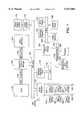
- FIG. 1illustrates a computer system incorporating a SCSI adapter which includes PCI-PCI interface logic according to the present invention
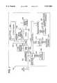
- FIG. 2is a more detailed block diagram of the SCSI adapter of FIG. 1, including a PCI bus interface controller according to the preferred embodiment of the present invention
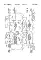
- FIG. 3illustrates the PCI to PCI interface system architecture of the present invention
- FIG. 4is a block diagram illustrating the PCI bus interface controller of FIG. 2;
- FIG. 5illustrates the data/address path of each respective dedicated PCI interface controller of FIG. 4;
- FIG. 6illustrates the data/address path of the DMA/XBUS data controller and local arbiter of FIG. 4;
- FIG. 7is a flowchart diagram illustrating operation of a method for accessing peripheral memory in an embedded controller during powerup of the computer system.
- the computer systemincludes a central processing unit (CPU) 102 which is coupled through a CPU local bus 104 to a host/PCI/cache bridge 106.
- the bridge 106couples through a memory bus 108 to main memory 110.
- the host/PCI/cache bridge 106also interfaces to a peripheral component interconnect (PCI) bus 120.
- PCIperipheral component interconnect
- a PCI local busis used.
- VESAVideo Electronics Standards Association
- a video adapter 170 and video frame buffer 172are coupled to the PCI bus 120 for controlling video functions.
- a SCSI (small computer systems interface) controller or SCSI adapter 122is coupled to the PCI bus 120.
- the SCSI adapter 122includes PCI to PCI interface logic according to the present invention.
- the SCSI adapter 122also includes peripheral devices which can be accessed by utilities executing on the host CPU 102 even when the adapter 122 is inoperable.
- a jumper 180is coupled to the SCSI adapter 122. The jumper 180 is set to allow host utilities to access peripheral device memory according to the present invention, as discussed further below.
- the SCSI controller or adapter 122may be integrated into the motherboard of the computer system or may be a separate adapter card insertable into the PCI bus 120.
- the terms adapter and controllerare intended to refer to either an embedded controller on the motherboard of the computer system or a controller on a removable adapter card.
- the SCSI adapter 122includes two SCSI channels 123 and 125. Each of these SCSI channels 123 and 125 may have various devices connected to them.
- the SCSI channel 123includes two disk drive units 124 and a tape drive 126.
- the SCSI channel 125includes two disk drive units 124 and a CD-ROM 128. It is noted that other devices may be connected to the SCSI channels 123 and 125, as desired.
- Various other devicesmay be connected to the PCI bus 120, such as a network interface card 140. As shown, the network interface card 140 interfaces to a local area network (LAN) 142.
- LANlocal area network
- Expansion bus bridge logic 150is also preferably coupled to the PCI bus 120.
- the expansion bus bridge logic 150interfaces to an expansion bus 152.
- the expansion busmay be any of varying types, including the industry standard architecture (ISA) bus, also referred to as the AT bus, the extended industry standard architecture (EISA) bus, or the microchannel architecture (MCA) bus.
- ISAindustry standard architecture
- EISAextended industry standard architecture
- MCAmicrochannel architecture
- Various devicesmay be coupled to the expansion bus 152, including expansion bus memory 154 and a modem 156.
- the expansion bus bridge logic 150also couples to a peripheral expansion bus referred to as the X-bus 160.
- the X-bus 160is used for connecting various peripherals to the computer system.
- an interrupt system 162a real time clock (RTC) and timers 164, a direct memory access (DMA) system 166, and ROM/Flash memory 168 are coupled to the X-bus 160.
- Other peripheralsare preferably connected to the X-bus 160, including communications ports, diagnostics ports, command/status registers, non-volatile static random access memory (NVSRAM), etc.
- FIG. 2a block diagram illustrating the SCSI adapter 122 in FIG. 1 is shown.
- PCI to PCI interface bridge logicaccording to the present invention is comprised within SCSI adapter 122.
- the PCI to PCI bridge logic of the present inventionmay be incorporated into various types of devices, including the network interface card 140, video adapter 170, and other types of devices.
- the SCSI adapter 122includes a PCI bus interface chip (interface chip) 202, which couples to the host or primary PCI bus 120.
- the interface chip 202includes the PCI to PCI interface logic of the present invention, which is discussed further below.
- the interface chip 202interfaces through a second X-bus 204 to various X-bus peripherals 206 as shown. It is noted that the X-bus 204 in the SCSI adapter 122 is different from the X-bus 160 in FIG. 1.
- the various X-bus peripherals 206preferably include a DMA system, interrupt system, timers, a real time clock (RTC), configuration ports, diagnostic ports, command/status registers, ROM/Flash memory, and non-volatile SRAM (NVSRAM) (all not shown).
- the interface chip 202also couples to a secondary PCI bus 210.
- the secondary PCI bus 210is different than the primary PCI bus 120.
- the secondary PCI bus 210is referred to as either the secondary PCI bus or the local PCI bus, and the primary PCI bus 210 is referred to as either the primary PCI bus or the host PCI bus.
- the term "local PCI bus" used to describe the bus 210should not be confused with the fact that the PCI bus itself can be classified as a local bus.
- SCSI controllers 212are coupled to the secondary PCI bus 210.
- the SCSI controllers 212in turn couple through a SCSI bus 214 to internal SCSI connectors 216.
- SCSI bus 214comprises the two SCSI channels 123 and 125.
- the internal SCSI connectors 216are for attaching the various devices, such as the disk drives 124, tape drive 126, and CD ROM 128, as shown in FIG. 1.
- a local CPU 220is coupled to the secondary PCI bus 210.
- the local CPU 220may be any of various types.
- the local CPU 220is the PowerPC microprocessor produced by Motorola, IBM and Apple.
- the local CPU 220is the Alpha chip from Digital Equipment Corporation (DEC).
- the local CPU 220couples through a serial bus to an SROM 222.
- the local CPU 220receives power from a 3.3V switching regulator 224, as shown.
- the local CPU 220includes a 64 bit data path which couples through a 64-bit data bus 230.
- Dynamic random access memory (DRAM) 236is coupled to the 64-bit data bus 230.
- DRAMDynamic random access memory
- the 64-bit data bus 230also includes a connection for coupling to an optional dynamic random access memory (DRAM) upgrade daughter card 234.
- DRAMdynamic random access memory
- An optional second level or L2 cache system 232may also be coupled to the 64-bit data bus 230.
- the DRAM upgrade daughter card 234 and the L2 cache system 232are shown in dotted lines and are options that are included in the preferred embodiment, but may be left out as desired.
- a battery backup controller 238is coupled to each of the DRAM 236 and the DRAM upgrade daughter card 234.
- the local PCI bus 210also includes a daughter card option for additional SCSI connections. As shown, additional PCI controllers 250 may be coupled to the local PCI bus 210 through a daughter card PCI bus as shown. The PCI controllers 250 couple through additional SCSI channels 252 to respective external SCSI connectors 254, as shown.
- Jumper 180connects to the interface chip 202 in the SCSI adapter 122.
- the interface chip 202configures itself as a memory device and maps in the memory of the peripheral devices.
- the jumper 180also causes the interface chip 202 to generate a signal to reset logic 272 which provides a reset signal to the reset input of the local CPU 220. This prevents the local CPU 220 from booting.
- a host utility executing on the host CPU 102can access memory in the peripheral devices.
- the interface chip 202includes a primary PCI interface 302 and a secondary PCI interface 304.
- the primary PCI interface 302interfaces to the host or primary PCI bus 120.
- the secondary PCI interface 304interfaces to the secondary or local PCI bus 210.
- the primary PCI interface 302 and secondary PCI interface 304interface to each other via a control handshake signal 305 as shown.
- the primary PCI interface 302also provides various bus signals over bus 306, including address, data, control and byte enable signals, referred to as A/D/C/BE.
- the secondary PCI interface 304provides bus signals, including address, data, control and byte enable signals, over bus 308.
- Data Queue 310is coupled between bus 306 and bus 308 to allow data communication between primary PCI interface 302 and secondary PCI interface 304.
- a bypass 312is coupled between each of the buses 306 and 308, and the primary PCI interface 302 and secondary PCI interface 304 provide their respective bus signals to each other through the bypass 312 as shown.
- the primary PCI interface 302 and secondary PCI interface 304also each provide their respective bus signals over buses 306 and 308 to a peripheral bus interface 314.
- the peripheral bus interface 314interfaces to an N bit peripheral bus, which is the X-bus 204.
- various peripheral devicesare connected to the N bit peripheral bus 204, including ROM/Flash memory 330 and non-volatile RAM 332 as shown, as well as direct memory access (DMA), controller logic, an interrupt subsystem, a real time clock, various timers, communication ports, diagnostic ports, command/status registers, etc.
- Jumper 180connects to the primary PCI interface 302, and the primary PCI interface 302 provides a signal to Reset logic 272.
- the Reset Logic 272provides a Reset signal to the local processor 220 as shown.
- the interface chip 202comprises a high performance host PCI to local PCI bus controller interface.
- the interface chip architecture of the present inventionincludes a symmetrical design for sharing DMA controller and peripheral extension bus (X-bus) resources between each PCI side.
- the primary PCI interface 302 and secondary PCI interface 304provide master/slave interfaces between each PCI side.
- the PCI interfaces 302 and 304symmetrically interface to the data queue 310 for DMA and/or burst cycles and symmetrically interface to the queue bypass buffer 312, which allows the PCI interfaces 302 and 304 to bridge directly.
- the PCI interfaces 302 and 304target the peripheral bus 204 based on address and configuration mapping, and the interfaces 302 and 304 arbitrate between each other for access to the peripheral bus 204.
- the symmetrical interface chip architecture of the present inventionprovides numerous advantages over those found in the prior art. For more information on some of these advantages, please see related co-pending application DC-00617, Ser. No. 08/319,207, titled “PCI/PCI Bus Interface Controller with Non-coupled Peripheral Slave Bus Extension", and filed Oct. 6, 1994, which is hereby incorporated by reference.
- primary and secondary PCI interfaces 302 and 304allows peripheral I/O devices to be accessed without having to cross PCI sides.
- host devices on the primary PCI interface 302can access devices on the peripheral X-bus 204 without having to arbitrate and gain access to the secondary PCI bus 210.
- Arbitration to gain access to the secondary PCI bus 210would be required in a PCI-PCI interface control system where the peripheral X-bus interface resided as unique target device on the secondary PCI bus 210. Since host devices do not have to gain access to the secondary PCI bus 210 to access peripheral devices, the peripheral devices can be accessed when the local processor 220 is unable to boot and/or the secondary bus 210 is inoperable.
- the system of the present inventionallows a host device to access Flash memory 330 or NVRAM 332 on the X-bus 204 when the local processor 220 is unable to boot and/or the secondary bus 210 is inoperable. Since the Flash memory 330 is accessible by the host, the Flash memory 330 can be reprogrammed by the host if it has become invalid or corrupted. This removes the need for the Flash device 330 to be socketed for removal in case it becomes corrupted or invalid and, as a result, the local processor 220 is unable to boot. Also, the system architecture of the present invention allows the Flash memory device 330 to be installed blank and then programmed by a host utility in the manufacturing process. This eliminates the cost of pre-programming the device prior to board installation. Further, the NVRAM 332 can be accessed for event log and failure information even if the SCSI adapter 122 is inoperable and the local processor 220 is unable to boot. This provides valuable failure information that many times is otherwise inaccessible.
- FIG. 4illustrates a presently preferred embodiment of the interface chip 202 of FIG. 2. Elements described in FIG. 4 which are similar to those in FIG. 3 include the same reference numerals for convenience.
- the interface chip 202includes primary PCI interface 302 and secondary PCI interface 304.
- the primary PCI interface 302 and the secondary PCI interface 304are comprised of the same logic chip, referred to as the Dual PCI Interface Controller (DPIC).
- the DPIC chipincludes a primary/secondary strappable pin which allows the chip to be used as separate host and local PCI interfaces in the interface chip 202, depending on the state of the pin.
- the DPIC configured as the primary PCI interface 302is referred to as the Host DPIC, and the DPIC configured as the secondary PCI interface 304 is referred to as the Local DPIC, as shown.
- the use of a single logic chip as the primary and secondary PCI interfaces 302 and 304reduces system costs.
- the primary PCI interface 302 and the secondary PCI interface 304communicate with each other via DPIC control handshake 305.
- Primary PCI interface 302couples to host UBUS 306 which includes address and data portions as well as control and byte enable portions.
- secondary PCI interface 304couples to local UBUS 308 as shown.
- the host UBUS 306connects to buffer 410 and likewise local UBUS 308 connects to buffer 412.
- the buffers 410 and 412are connected via a FIFO out bus 414.
- the FIFO out bus 414connects to data queue 310.
- the data queue 310is preferably a synchronous 256 ⁇ 36 bit single channel FIFO data queue. However, it is noted that other data queues may be used as desired.
- the primary PCI interface 302 and secondary interface 304also are coupled through a control bus referred to as the DXAC/FIFO control bus 420.
- the DXAC/FIFO control bus 420couples to the data queue 310 and also connects to DMA/XBUS controller logic 422, also referred to as the DXAC.
- the DMA/XBUS controller logic 422generates X-bus control signal, X-bus request signals referred to as SREQ 5:0!, and grant signals referred to SGNT 5:0!.
- the host UBUS 306connects to a transceiver 430 which connects to a DXAC bus 432.
- the local UBUS 308connects to transceiver 434, which couples to the DXAC bus 432.
- the DXAC bus 432couples to the DMA/XBUS controller logic 422.
- the data queue 310is coupled to the DMA/XBUS controller 422 via a FIFO In bus 440.
- the FIFO In bus 440couples to an X-bus buffer 442 which in turn provides X-bus addressing signals XA 19:2! and X-bus data signals XD 7:0!.
- the various logic comprised in the interface chip 202preferably receives a 33 MHz CLK signal from the host PCI bus through CLK buffer 450.
- the Host and Local DPIC 302 and 304are each responsible for PCI bus mastering and bus target slave control on the respective host and local PCI sides of the SCSI controller 122. In the preferred embodiment, all PCI data and address transactions are completed through the DPIC.
- the primary (host) and secondary (local) DPICs 302 and 304arbitrate between each other for the respective interface chip UBUS 306 and 308 and X-bus 204. These interfaces are preferably slaves to the DMA/XBUS (DXAC) controller 422.
- the DPICsare PCI masters for all DMA transactions.
- Jumper 180connects to the primary PCI interface 302, and the primary PCI interface 302 provides a signal to Reset logic 272.
- the Reset Logic 272provides a Reset signal to the local processor 220 (not shown).
- each DPIC 302 and 304connects on one side to a PCI bus and on another side to a UBUS.
- the address, data and byte enable signals of the UBUSare connected to a 4:1 multiplexer 502.
- a memory map block referred to as Map A Address 504also provides input to the multiplexer 502.
- the Map A Address block 504provides addressing to a 256 Kbyte region accessible on the host side, and this region is the primary memory region used by host drivers to access the SCSI controller 122.
- the multiplexer 502provides output to an N+1 FIFO posting register 506.
- the register 506in turn provides output back to an input of the multiplexer 502 as shown.
- the register 506also provides output to a 3:1 multiplexer 510.
- the UBUSalso provides signals that are connected to an input of the multiplexer 510.
- the multiplexer 510provides output to a PCI output register 512 which in turn provides output back to the multiplexer 510.
- the register 512also provides output to the PCI bus, as shown.
- the PCI busis coupled to a second 3:1 multiplexer 540.
- the output of the multiplexer 510also provides input to the multiplexer 540.
- Multiplexer 540provides an output to an address/data posting register 542, which is coupled to a bus 530.
- the bus 530provides input to the multiplexer 540.
- the bus 530couples to prefix address register/comparator and retry counter 544 and parity generator checking logic 546, as shown.
- the parity generator/checking logic 546provides a parity error signal on the PCI bus as shown.
- the register 542provides an output over bus 530 to a second 4:1 multiplexer 550.
- the multiplexer 550also receives input from the PCI bus and from a Map B address block 552.
- the Map B address block 552provides addressing for a 256 Kbyte region accessible on the SCSI controller local side which is used by the SCSI controller 122 to maintain fill PCI address compatibility.
- the multiplexer 550provides output to a UBUS output register 554, which in turn provides output back into the multiplexer 550.
- the UBUS output register 554also couples to the UBUS.
- UBUS control signalsare coupled to UBUS state machine and control logic 520, and PCI control signals are provided to PCI master/slave state machine and control logic 522.
- the UBUS state machine and control logic 520is coupled to the PCI master/slave state machine and control logic 522 via a bus 524.
- the bus 524couples to configuration and control registers 526 and address comparator/decode logic 528.
- the configuration and control registers 526provide output to the multiplexer 502.
- the configuration and control registers 526couple to the address comparator/decode logic 528 via bus 530.
- FIG. 6a block diagram illustrating the address path of the DMA/XBUS controller (DXAC) 422 is shown.
- the UBUSis connected to a DMA byte lane alignment multiplexer 604.
- the multiplexer 604provides output to a 2:1 multiplexer 606 and also provides output to a second 4:1 multiplexer 612.
- the multiplexer 606provides output to an X-bus/DMA posting register 608.
- the register 608provides output to the multiplexer 606 and to an X-bus write byte shift 4:1 multiplexer 614.
- the multiplexer 614provides an output to the multiplexer 612.
- the multiplexer 612provides an output to a FIFO X-bus output register 616, which in turn provides an output back to the multiplexer 612.
- the register 616also provides output to the FIFO bus 440 and correspondingly to the X-bus 204.
- the register 608further provides output to X-bus chip select logic 620 which provides a chip select signal out onto the X-bus.
- the register 608also provides an output to configuration control and DMA address registers 630.
- the registers 630provide output to a 4:1 multiplexer 634.
- the FIFO/X-busprovides two inputs to the multiplexer 634.
- the multiplexerprovides an output to a UBUS output register 636 which provides an output back to an input of the multiplexer 634.
- the register 636also provides an output to the register block 630.
- the UBUS output register 636also couples to the UBUS as shown.
- the configuration control and DMA address registers 630are coupled to DMA counter state machine and control logic 640 via a bus 642.
- the bus 642also couples to UBUS state machine and control logic 644, which couples to the control portion of the UBUS.
- the bus 642also couples to FIFO/X-bus state machine and control logic 646 which couples to the control portion of the FIFO/X-bus 440.
- Local PCI bus master arbiter logic 650is coupled to the control portion of the local PCI bus and the request/GNT portion of the local PCI bus.
- FIG. 7a flowchart diagram illustrating operation of a method for enabling the host CPU 102 to access peripheral devices in the bus adapter 122 even when the local processor 220 is unable to boot and/or the secondary bus is inaccessible is shown.
- the method of the present inventionupdates the Flash memory 330 independently of the secondary local bus 210 and/or local processor 220. This provides a cost-effective and efficient mechanism for restoring code in the Flash device 330 if the Flash device 330 has become corrupted and as a result, the local processor 220 is unable to boot.
- Thisalso enables the Flash memory 330 to be programmed for the first time during manufacturing. In other words, the Flash memory device 330 can be installed blank and then later programmed by a host utility in the manufacturing process.
- the present inventionalso allows the host CPU 102 to access the NVRAM 332 to obtain event failure information even if the local processor 220 is unable to boot and/or the secondary PCI bus 210 has failed. As discussed in the background section, many failed controllers that are returned include little or no data describing the conditions prior to failure because the event logs are typically inaccessible. The present invention allows much greater access to these event logs in many diverse types of bus adapter failures.
- jumper 180is set to direct the primary PCI interface to configure itself as a memory device and to map the memory of the peripheral devices into the primary PCI interface 302.
- subsequent CPUreads or writes to the primary PCI interface 302 while the jumper 180 is set actually access memory in selected peripheral devices such as Flash memory 330 or NVRAM 332, depending on the host utility.
- the result of setting the jumper 180is to make the Flash device 330, NVRAM 332 and the memory of other peripheral devices accessible by the host CPU 102.
- the jumper 180provides both memory and I/O mapping in systems which support both memory and I/O mapping, such as systems using Intel CPUs. In other systems which include only memory mapping, such as RISC systems or Apple systems, the jumper only provides a memory map to the peripheral devices.
- step 704the CPU begins its POST (power on self test) procedure.
- the hostviews the memory in the primary PCI interface 302 and in step 708 the host CPU 102 maps this memory into its local memory.
- the CPU 102preferably maps a 16 Kbyte memory block window into its local memory so that future host utilities can access memory in the peripheral devices. Since the host CPU 102 only maps a 16 Kbyte window corresponding to the memory of the peripheral devices into its local memory, the host CPU 102 only "sees" a 16 Kbyte window of the actual peripheral device memory.
- the DXAC chip 422includes a register referred to as the X-bus Paging Register that is used to adjust this 16 Kbyte window to access the memory of different peripheral devices or to access different portions of the memory of a peripheral device.
- the Flash device 330is actually 512 Kbytes, and thus the CPU 102 is required to do 32 16 Kbyte writes to reprogram the Flash memory.
- a desired applicationexecutes on the host CPU 102 which accesses the desired peripheral in the SCSI adapter 122.
- the CPU 102accesses, i.e., reads or writes, memory in the primary PCI interface 302, and the primary PCI interface 302 in turn accesses the desired peripheral device.
- the primary PCI interface 302receives the write data in a posting register and transfers the write data to the desired peripheral.
- the primary PCI interface 302receives the read request and the addresses corresponding to the desired data, obtains the requested data from the respective peripheral device, and provides the requested data to the CPU 102.
- the interface chip 202uses the X-bus paging register discussed above to increment through 16 Kbyte windows of data to perform the transfer.
- Flash memory 330Various types of applications can execute in step 710 to access desired peripheral devices.
- one applicationprograms the Flash memory 330. This is preferably for cases where Flash memory 330 was installed blank and needs to be programmed or has become corrupted and/or contains invalid code.
- the Flash memory 330is accessible even when local processor 220 is unable to boot and/or the bus adapter 122 is inoperable.
- Another applicationwhich may execute in step 710 reads the NVRAM 332 to obtain event log and failure information.
- step 712the jumper 180 is removed or reset, which unmaps the peripheral device memory and returns the adapter 122 to the appearance of a SCSI controller 122.
- step 714the system is rebooted, and the host CPU 102 again begins its POST procedure.
- step 716the CPU 102 sees the primary PCI interface 302 in the adapter 122 as a SCSI controller, and operation proceeds normally.
Landscapes
- Engineering & Computer Science (AREA)
- Theoretical Computer Science (AREA)
- General Engineering & Computer Science (AREA)
- Quality & Reliability (AREA)
- Physics & Mathematics (AREA)
- General Physics & Mathematics (AREA)
- Computer Hardware Design (AREA)
- Debugging And Monitoring (AREA)
- Bus Control (AREA)
Abstract
Description
Claims (21)
Priority Applications (1)
| Application Number | Priority Date | Filing Date | Title |
|---|---|---|---|
| US09/024,719US5911084A (en) | 1994-10-07 | 1998-02-17 | System and method for accessing peripheral devices on a non-functional controller |
Applications Claiming Priority (2)
| Application Number | Priority Date | Filing Date | Title |
|---|---|---|---|
| US08/319,689US5729767A (en) | 1994-10-07 | 1994-10-07 | System and method for accessing peripheral devices on a non-functional controller |
| US09/024,719US5911084A (en) | 1994-10-07 | 1998-02-17 | System and method for accessing peripheral devices on a non-functional controller |
Related Parent Applications (1)
| Application Number | Title | Priority Date | Filing Date |
|---|---|---|---|
| US08/319,689DivisionUS5729767A (en) | 1994-10-07 | 1994-10-07 | System and method for accessing peripheral devices on a non-functional controller |
Publications (1)
| Publication Number | Publication Date |
|---|---|
| US5911084Atrue US5911084A (en) | 1999-06-08 |
Family
ID=23243282
Family Applications (2)
| Application Number | Title | Priority Date | Filing Date |
|---|---|---|---|
| US08/319,689Expired - LifetimeUS5729767A (en) | 1994-10-07 | 1994-10-07 | System and method for accessing peripheral devices on a non-functional controller |
| US09/024,719Expired - LifetimeUS5911084A (en) | 1994-10-07 | 1998-02-17 | System and method for accessing peripheral devices on a non-functional controller |
Family Applications Before (1)
| Application Number | Title | Priority Date | Filing Date |
|---|---|---|---|
| US08/319,689Expired - LifetimeUS5729767A (en) | 1994-10-07 | 1994-10-07 | System and method for accessing peripheral devices on a non-functional controller |
Country Status (1)
| Country | Link |
|---|---|
| US (2) | US5729767A (en) |
Cited By (23)
| Publication number | Priority date | Publication date | Assignee | Title |
|---|---|---|---|---|
| US6021483A (en)* | 1997-03-17 | 2000-02-01 | International Business Machines Corporation | PCI-to-PCI bridges with a timer register for storing a delayed transaction latency |
| US6065085A (en)* | 1998-01-27 | 2000-05-16 | Lsi Logic Corporation | Bus bridge architecture for a data processing system capable of sharing processing load among a plurality of devices |
| US6076130A (en)* | 1998-03-19 | 2000-06-13 | Hewlett-Packard Company | System and method for efficient communication between buses |
| FR2796478A1 (en)* | 1999-07-13 | 2001-01-19 | Thomson Training & Simulation | MULTIPROCESSOR COMPUTER SYSTEM |
| US20030018889A1 (en)* | 2001-07-20 | 2003-01-23 | Burnett Keith L. | Automated establishment of addressability of a network device for a target network enviroment |
| US6553432B1 (en) | 1999-10-26 | 2003-04-22 | Dell Usa, L.P. | Method and system for selecting IDE devices |
| US20030191978A1 (en)* | 2002-04-04 | 2003-10-09 | International Business Machines Corporation | Multiple fault location in a series of devices |
| US20030204780A1 (en)* | 2002-04-25 | 2003-10-30 | International Business Machines Corporation | Handling multiple operating system capabilities in a logical partition data processing system |
| WO2002077817A3 (en)* | 2001-03-22 | 2004-01-15 | I Bus Phoenix Inc | Fault tolerant hybrid switching architecture coupling pci buses and processors |
| US20040059862A1 (en)* | 2002-09-24 | 2004-03-25 | I-Bus Corporation | Method and apparatus for providing redundant bus control |
| US6725312B1 (en) | 2000-11-02 | 2004-04-20 | Cml Versatel Inc. | Bus architecture for high reliability communications in computer system |
| US6728822B1 (en)* | 1999-03-12 | 2004-04-27 | International Business Machines Corporation | Bus bridge circuit, information processing system and cardbus controller |
| US6745243B2 (en)* | 1998-06-30 | 2004-06-01 | Nortel Networks Limited | Method and apparatus for network caching and load balancing |
| US20040230878A1 (en)* | 2003-05-14 | 2004-11-18 | Mantey Paul John | Detecting and diagnosing a malfunctioning host coupled to a communications bus |
| US20040250035A1 (en)* | 2003-06-06 | 2004-12-09 | Atkinson Lee W. | Method and apparatus for affecting computer system |
| US20040268359A1 (en)* | 2003-06-27 | 2004-12-30 | Hanes David H. | Computer-readable medium, method and computer system for processing input/output requests |
| US20050060472A1 (en)* | 2003-09-12 | 2005-03-17 | Mantey Paul J. | Communications bus transceiver |
| US6981079B2 (en) | 2002-03-21 | 2005-12-27 | International Business Machines Corporation | Critical datapath error handling in a multiprocessor architecture |
| US20060026211A1 (en)* | 2004-07-30 | 2006-02-02 | United Parcel Service Of America, Inc. | Systems, methods, computer readable medium and apparatus for memory management using NVRAM |
| WO2006019330A1 (en)* | 2004-07-16 | 2006-02-23 | Intel Corporation | Techniques to store configuration information in an option read-only memory |
| US20130013820A1 (en)* | 2011-07-04 | 2013-01-10 | Stmicroelectronics (Rousset) Sas | Method for initializing registers of peripherals in a microcontroller |
| US20140013028A1 (en)* | 2012-07-09 | 2014-01-09 | Hamilton Sundstrand Corporation | Hardware flash memory wear monitoring |
| CN107656887A (en)* | 2016-07-25 | 2018-02-02 | 中兴通讯股份有限公司 | The control device and method of peripheral bus |
Families Citing this family (13)
| Publication number | Priority date | Publication date | Assignee | Title |
|---|---|---|---|---|
| US6924790B1 (en) | 1995-10-16 | 2005-08-02 | Nec Corporation | Mode switching for pen-based computer systems |
| US5759102A (en)* | 1996-02-12 | 1998-06-02 | International Game Technology | Peripheral device download method and apparatus |
| US6253334B1 (en)* | 1997-05-13 | 2001-06-26 | Micron Electronics, Inc. | Three bus server architecture with a legacy PCI bus and mirrored I/O PCI buses |
| US5918073A (en)* | 1997-06-27 | 1999-06-29 | Advanced Micro Devices, Inc. | System and method for equalizing data buffer storage and fetch rates of peripheral devices |
| KR100448932B1 (en)* | 1997-09-23 | 2004-12-17 | 삼성전자주식회사 | Flash ROM Writer Device and Control Method |
| US6141757A (en)* | 1998-06-22 | 2000-10-31 | Motorola, Inc. | Secure computer with bus monitoring system and methods |
| US6625747B1 (en) | 2000-06-30 | 2003-09-23 | Dell Products L.P. | Computer storage system and failover method |
| US7194663B2 (en)* | 2003-11-18 | 2007-03-20 | Honeywell International, Inc. | Protective bus interface and method |
| CN1926521B (en)* | 2004-03-18 | 2010-10-06 | 英特尔公司 | Method and device to support booting despite deficient resources |
| US8639855B2 (en)* | 2008-10-20 | 2014-01-28 | International Business Machines Corporation | Information collection and storage for single core chips to 'N core chips |
| US9665468B2 (en)* | 2013-08-19 | 2017-05-30 | Intel Corporation | Systems and methods for invasive debug of a processor without processor execution of instructions |
| WO2019152037A1 (en)* | 2018-02-01 | 2019-08-08 | Hewlett-Packard Development Company, L.P. | Instruction updates via side channels |
| CN114281722B (en)* | 2021-12-29 | 2024-04-05 | 合肥市芯海电子科技有限公司 | Embedded control circuit with double bus interfaces, chip and electronic equipment |
Citations (10)
| Publication number | Priority date | Publication date | Assignee | Title |
|---|---|---|---|---|
| US4484263A (en)* | 1981-09-25 | 1984-11-20 | Data General Corporation | Communications controller |
| US4736373A (en)* | 1981-08-03 | 1988-04-05 | Pacific Western Systems, Inc. | Memory tester having concurrent failure data readout and memory repair analysis |
| US4740882A (en)* | 1986-06-27 | 1988-04-26 | Environmental Computer Systems, Inc. | Slave processor for controlling environments |
| US5019799A (en)* | 1981-08-06 | 1991-05-28 | Nissan Motor Company, Limited | Electronic device with self-monitor for an automotive vehicle |
| US5047921A (en)* | 1989-01-31 | 1991-09-10 | International Business Machines Corporation | Asynchronous microprocessor random access memory arbitration controller |
| US5054024A (en)* | 1989-08-09 | 1991-10-01 | Texas Instruments Incorporated | System scan path architecture with remote bus controller |
| US5056093A (en)* | 1989-08-09 | 1991-10-08 | Texas Instruments Incorporated | System scan path architecture |
| US5197034A (en)* | 1991-05-10 | 1993-03-23 | Intel Corporation | Floating gate non-volatile memory with deep power down and write lock-out |
| US5361343A (en)* | 1991-07-30 | 1994-11-01 | Intel Corporation | Microprocessor system including first and second nonvolatile memory arrays which may be simultaneously read and reprogrammed |
| US5396602A (en)* | 1993-05-28 | 1995-03-07 | International Business Machines Corp. | Arbitration logic for multiple bus computer system |
- 1994
- 1994-10-07USUS08/319,689patent/US5729767A/ennot_activeExpired - Lifetime
- 1998
- 1998-02-17USUS09/024,719patent/US5911084A/ennot_activeExpired - Lifetime
Patent Citations (10)
| Publication number | Priority date | Publication date | Assignee | Title |
|---|---|---|---|---|
| US4736373A (en)* | 1981-08-03 | 1988-04-05 | Pacific Western Systems, Inc. | Memory tester having concurrent failure data readout and memory repair analysis |
| US5019799A (en)* | 1981-08-06 | 1991-05-28 | Nissan Motor Company, Limited | Electronic device with self-monitor for an automotive vehicle |
| US4484263A (en)* | 1981-09-25 | 1984-11-20 | Data General Corporation | Communications controller |
| US4740882A (en)* | 1986-06-27 | 1988-04-26 | Environmental Computer Systems, Inc. | Slave processor for controlling environments |
| US5047921A (en)* | 1989-01-31 | 1991-09-10 | International Business Machines Corporation | Asynchronous microprocessor random access memory arbitration controller |
| US5054024A (en)* | 1989-08-09 | 1991-10-01 | Texas Instruments Incorporated | System scan path architecture with remote bus controller |
| US5056093A (en)* | 1989-08-09 | 1991-10-08 | Texas Instruments Incorporated | System scan path architecture |
| US5197034A (en)* | 1991-05-10 | 1993-03-23 | Intel Corporation | Floating gate non-volatile memory with deep power down and write lock-out |
| US5361343A (en)* | 1991-07-30 | 1994-11-01 | Intel Corporation | Microprocessor system including first and second nonvolatile memory arrays which may be simultaneously read and reprogrammed |
| US5396602A (en)* | 1993-05-28 | 1995-03-07 | International Business Machines Corp. | Arbitration logic for multiple bus computer system |
Cited By (35)
| Publication number | Priority date | Publication date | Assignee | Title |
|---|---|---|---|---|
| US6021483A (en)* | 1997-03-17 | 2000-02-01 | International Business Machines Corporation | PCI-to-PCI bridges with a timer register for storing a delayed transaction latency |
| US6065085A (en)* | 1998-01-27 | 2000-05-16 | Lsi Logic Corporation | Bus bridge architecture for a data processing system capable of sharing processing load among a plurality of devices |
| US6223240B1 (en)* | 1998-01-27 | 2001-04-24 | Lsi Logic Corporation | Bus bridge architecture for a data processing system capable of sharing processing load among a plurality of devices |
| US6076130A (en)* | 1998-03-19 | 2000-06-13 | Hewlett-Packard Company | System and method for efficient communication between buses |
| US6745243B2 (en)* | 1998-06-30 | 2004-06-01 | Nortel Networks Limited | Method and apparatus for network caching and load balancing |
| US6728822B1 (en)* | 1999-03-12 | 2004-04-27 | International Business Machines Corporation | Bus bridge circuit, information processing system and cardbus controller |
| FR2796478A1 (en)* | 1999-07-13 | 2001-01-19 | Thomson Training & Simulation | MULTIPROCESSOR COMPUTER SYSTEM |
| US6553432B1 (en) | 1999-10-26 | 2003-04-22 | Dell Usa, L.P. | Method and system for selecting IDE devices |
| US6725312B1 (en) | 2000-11-02 | 2004-04-20 | Cml Versatel Inc. | Bus architecture for high reliability communications in computer system |
| US6950893B2 (en) | 2001-03-22 | 2005-09-27 | I-Bus Corporation | Hybrid switching architecture |
| WO2002077817A3 (en)* | 2001-03-22 | 2004-01-15 | I Bus Phoenix Inc | Fault tolerant hybrid switching architecture coupling pci buses and processors |
| US20060031625A1 (en)* | 2001-03-22 | 2006-02-09 | I-Bus Corporation | Hybrid switching architecture |
| US20040225785A1 (en)* | 2001-03-22 | 2004-11-11 | I-Bus/Phoenix, Inc. | Hybrid switching architecture |
| US7313819B2 (en)* | 2001-07-20 | 2007-12-25 | Intel Corporation | Automated establishment of addressability of a network device for a target network environment |
| US20030018889A1 (en)* | 2001-07-20 | 2003-01-23 | Burnett Keith L. | Automated establishment of addressability of a network device for a target network enviroment |
| US6981079B2 (en) | 2002-03-21 | 2005-12-27 | International Business Machines Corporation | Critical datapath error handling in a multiprocessor architecture |
| US20030191978A1 (en)* | 2002-04-04 | 2003-10-09 | International Business Machines Corporation | Multiple fault location in a series of devices |
| US6920587B2 (en) | 2002-04-25 | 2005-07-19 | International Business Machines Corporation | Handling multiple operating system capabilities in a logical partition data processing system |
| US20030204780A1 (en)* | 2002-04-25 | 2003-10-30 | International Business Machines Corporation | Handling multiple operating system capabilities in a logical partition data processing system |
| US20040059862A1 (en)* | 2002-09-24 | 2004-03-25 | I-Bus Corporation | Method and apparatus for providing redundant bus control |
| US7200781B2 (en) | 2003-05-14 | 2007-04-03 | Hewlett-Packard Development Company, L.P. | Detecting and diagnosing a malfunctioning host coupled to a communications bus |
| US20040230878A1 (en)* | 2003-05-14 | 2004-11-18 | Mantey Paul John | Detecting and diagnosing a malfunctioning host coupled to a communications bus |
| US20040250035A1 (en)* | 2003-06-06 | 2004-12-09 | Atkinson Lee W. | Method and apparatus for affecting computer system |
| US20040268359A1 (en)* | 2003-06-27 | 2004-12-30 | Hanes David H. | Computer-readable medium, method and computer system for processing input/output requests |
| US20050060472A1 (en)* | 2003-09-12 | 2005-03-17 | Mantey Paul J. | Communications bus transceiver |
| US7676621B2 (en) | 2003-09-12 | 2010-03-09 | Hewlett-Packard Development Company, L.P. | Communications bus transceiver |
| WO2006019330A1 (en)* | 2004-07-16 | 2006-02-23 | Intel Corporation | Techniques to store configuration information in an option read-only memory |
| US8667214B2 (en) | 2004-07-16 | 2014-03-04 | Intel Corporation | Techniques to store configuration information in an option read-only memory |
| US9086893B2 (en) | 2004-07-16 | 2015-07-21 | Intel Corporation | Techniques to store configuration information in an option read-only memory |
| US20060026211A1 (en)* | 2004-07-30 | 2006-02-02 | United Parcel Service Of America, Inc. | Systems, methods, computer readable medium and apparatus for memory management using NVRAM |
| US7562202B2 (en) | 2004-07-30 | 2009-07-14 | United Parcel Service Of America, Inc. | Systems, methods, computer readable medium and apparatus for memory management using NVRAM |
| US20130013820A1 (en)* | 2011-07-04 | 2013-01-10 | Stmicroelectronics (Rousset) Sas | Method for initializing registers of peripherals in a microcontroller |
| US8677033B2 (en)* | 2011-07-04 | 2014-03-18 | Stmicroelectronics (Rousset) Sas | Method for initializing registers of peripherals in a microcontroller |
| US20140013028A1 (en)* | 2012-07-09 | 2014-01-09 | Hamilton Sundstrand Corporation | Hardware flash memory wear monitoring |
| CN107656887A (en)* | 2016-07-25 | 2018-02-02 | 中兴通讯股份有限公司 | The control device and method of peripheral bus |
Also Published As
| Publication number | Publication date |
|---|---|
| US5729767A (en) | 1998-03-17 |
Similar Documents
| Publication | Publication Date | Title |
|---|---|---|
| US5911084A (en) | System and method for accessing peripheral devices on a non-functional controller | |
| KR100262677B1 (en) | ADD-IN Board With Enable/Disable Expansion ROM for PCI BUS Computer | |
| US5499346A (en) | Bus-to-bus bridge for a multiple bus information handling system that optimizes data transfers between a system bus and a peripheral bus | |
| EP0836724B1 (en) | Add-in board with programmable configuration registers for pci bus computers | |
| US5761458A (en) | Intelligent bus bridge for input/output subsystems in a computer system | |
| US5905888A (en) | Bootable redundant hard disk attached to a PC's parallel port with rom-address auto-detect and configure during BIOS scan | |
| US7149823B2 (en) | System and method for direct memory access from host without processor intervention wherein automatic access to memory during host start up does not occur | |
| US4991085A (en) | Personal computer bus interface chip with multi-function address relocation pins | |
| US5802269A (en) | Method and apparatus for power management of distributed direct memory access (DDMA) devices | |
| EP0591437B1 (en) | Multiprocessor distributed initialization and self-test system | |
| US6529989B1 (en) | Intelligent expansion ROM sharing bus subsystem | |
| US9052916B2 (en) | System ROM with an embedded disk image | |
| US7890690B2 (en) | System and method for dual-ported flash memory | |
| US5987536A (en) | Computer system having flash memory bios which can be accessed while protected mode operating system is running | |
| JP3403284B2 (en) | Information processing system and control method thereof | |
| US5634079A (en) | System for providing for a parallel port with standard signals and a flash recovery mode with second predetermined signals redefining parallel port with alternate functions | |
| EP0661637A1 (en) | Configuration and RAM/ROM control of daughter card residing on adapter card | |
| US20010018721A1 (en) | Upgrade card for a computer system | |
| US7100088B2 (en) | Computer system equipped with a BIOS debugging card | |
| JPH05257657A (en) | Sequencer at power on | |
| US5809260A (en) | Burst mode data transmission retry of previously aborted block transfer of data | |
| US7249253B2 (en) | Booting from a re-programmable memory on an unconfigured bus | |
| US5933613A (en) | Computer system and inter-bus control circuit | |
| US6757770B1 (en) | Computer system supporting a universal serial bus (USB) interface and method for controlling a USB corresponding I/O device | |
| US20040153810A1 (en) | Computer system equipped with a BIOS debugging card |
Legal Events
| Date | Code | Title | Description |
|---|---|---|---|
| STCF | Information on status: patent grant | Free format text:PATENTED CASE | |
| FPAY | Fee payment | Year of fee payment:4 | |
| FEPP | Fee payment procedure | Free format text:PAYOR NUMBER ASSIGNED (ORIGINAL EVENT CODE: ASPN); ENTITY STATUS OF PATENT OWNER: LARGE ENTITY | |
| FPAY | Fee payment | Year of fee payment:8 | |
| FPAY | Fee payment | Year of fee payment:12 | |
| AS | Assignment | Owner name:BANK OF AMERICA, N.A., AS ADMINISTRATIVE AGENT, TE Free format text:PATENT SECURITY AGREEMENT (ABL);ASSIGNORS:DELL INC.;APPASSURE SOFTWARE, INC.;ASAP SOFTWARE EXPRESS, INC.;AND OTHERS;REEL/FRAME:031898/0001 Effective date:20131029 Owner name:BANK OF AMERICA, N.A., AS COLLATERAL AGENT, NORTH CAROLINA Free format text:PATENT SECURITY AGREEMENT (TERM LOAN);ASSIGNORS:DELL INC.;APPASSURE SOFTWARE, INC.;ASAP SOFTWARE EXPRESS, INC.;AND OTHERS;REEL/FRAME:031899/0261 Effective date:20131029 Owner name:BANK OF NEW YORK MELLON TRUST COMPANY, N.A., AS FIRST LIEN COLLATERAL AGENT, TEXAS Free format text:PATENT SECURITY AGREEMENT (NOTES);ASSIGNORS:APPASSURE SOFTWARE, INC.;ASAP SOFTWARE EXPRESS, INC.;BOOMI, INC.;AND OTHERS;REEL/FRAME:031897/0348 Effective date:20131029 Owner name:BANK OF AMERICA, N.A., AS ADMINISTRATIVE AGENT, TEXAS Free format text:PATENT SECURITY AGREEMENT (ABL);ASSIGNORS:DELL INC.;APPASSURE SOFTWARE, INC.;ASAP SOFTWARE EXPRESS, INC.;AND OTHERS;REEL/FRAME:031898/0001 Effective date:20131029 Owner name:BANK OF NEW YORK MELLON TRUST COMPANY, N.A., AS FI Free format text:PATENT SECURITY AGREEMENT (NOTES);ASSIGNORS:APPASSURE SOFTWARE, INC.;ASAP SOFTWARE EXPRESS, INC.;BOOMI, INC.;AND OTHERS;REEL/FRAME:031897/0348 Effective date:20131029 Owner name:BANK OF AMERICA, N.A., AS COLLATERAL AGENT, NORTH Free format text:PATENT SECURITY AGREEMENT (TERM LOAN);ASSIGNORS:DELL INC.;APPASSURE SOFTWARE, INC.;ASAP SOFTWARE EXPRESS, INC.;AND OTHERS;REEL/FRAME:031899/0261 Effective date:20131029 | |
| AS | Assignment | Owner name:ASAP SOFTWARE EXPRESS, INC., ILLINOIS Free format text:RELEASE BY SECURED PARTY;ASSIGNOR:BANK OF AMERICA, N.A., AS ADMINISTRATIVE AGENT;REEL/FRAME:040065/0216 Effective date:20160907 Owner name:WYSE TECHNOLOGY L.L.C., CALIFORNIA Free format text:RELEASE BY SECURED PARTY;ASSIGNOR:BANK OF AMERICA, N.A., AS ADMINISTRATIVE AGENT;REEL/FRAME:040065/0216 Effective date:20160907 Owner name:SECUREWORKS, INC., GEORGIA Free format text:RELEASE BY SECURED PARTY;ASSIGNOR:BANK OF AMERICA, N.A., AS ADMINISTRATIVE AGENT;REEL/FRAME:040065/0216 Effective date:20160907 Owner name:FORCE10 NETWORKS, INC., CALIFORNIA Free format text:RELEASE BY SECURED PARTY;ASSIGNOR:BANK OF AMERICA, N.A., AS ADMINISTRATIVE AGENT;REEL/FRAME:040065/0216 Effective date:20160907 Owner name:CREDANT TECHNOLOGIES, INC., TEXAS Free format text:RELEASE BY SECURED PARTY;ASSIGNOR:BANK OF AMERICA, N.A., AS ADMINISTRATIVE AGENT;REEL/FRAME:040065/0216 Effective date:20160907 Owner name:APPASSURE SOFTWARE, INC., VIRGINIA Free format text:RELEASE BY SECURED PARTY;ASSIGNOR:BANK OF AMERICA, N.A., AS ADMINISTRATIVE AGENT;REEL/FRAME:040065/0216 Effective date:20160907 Owner name:PEROT SYSTEMS CORPORATION, TEXAS Free format text:RELEASE BY SECURED PARTY;ASSIGNOR:BANK OF AMERICA, N.A., AS ADMINISTRATIVE AGENT;REEL/FRAME:040065/0216 Effective date:20160907 Owner name:DELL MARKETING L.P., TEXAS Free format text:RELEASE BY SECURED PARTY;ASSIGNOR:BANK OF AMERICA, N.A., AS ADMINISTRATIVE AGENT;REEL/FRAME:040065/0216 Effective date:20160907 Owner name:DELL PRODUCTS L.P., TEXAS Free format text:RELEASE BY SECURED PARTY;ASSIGNOR:BANK OF AMERICA, N.A., AS ADMINISTRATIVE AGENT;REEL/FRAME:040065/0216 Effective date:20160907 Owner name:COMPELLANT TECHNOLOGIES, INC., MINNESOTA Free format text:RELEASE BY SECURED PARTY;ASSIGNOR:BANK OF AMERICA, N.A., AS ADMINISTRATIVE AGENT;REEL/FRAME:040065/0216 Effective date:20160907 Owner name:DELL SOFTWARE INC., CALIFORNIA Free format text:RELEASE BY SECURED PARTY;ASSIGNOR:BANK OF AMERICA, N.A., AS ADMINISTRATIVE AGENT;REEL/FRAME:040065/0216 Effective date:20160907 Owner name:DELL USA L.P., TEXAS Free format text:RELEASE BY SECURED PARTY;ASSIGNOR:BANK OF AMERICA, N.A., AS ADMINISTRATIVE AGENT;REEL/FRAME:040065/0216 Effective date:20160907 Owner name:DELL INC., TEXAS Free format text:RELEASE BY SECURED PARTY;ASSIGNOR:BANK OF AMERICA, N.A., AS ADMINISTRATIVE AGENT;REEL/FRAME:040065/0216 Effective date:20160907 | |
| AS | Assignment | Owner name:APPASSURE SOFTWARE, INC., VIRGINIA Free format text:RELEASE BY SECURED PARTY;ASSIGNOR:BANK OF AMERICA, N.A., AS COLLATERAL AGENT;REEL/FRAME:040040/0001 Effective date:20160907 Owner name:SECUREWORKS, INC., GEORGIA Free format text:RELEASE BY SECURED PARTY;ASSIGNOR:BANK OF AMERICA, N.A., AS COLLATERAL AGENT;REEL/FRAME:040040/0001 Effective date:20160907 Owner name:DELL MARKETING L.P., TEXAS Free format text:RELEASE BY SECURED PARTY;ASSIGNOR:BANK OF AMERICA, N.A., AS COLLATERAL AGENT;REEL/FRAME:040040/0001 Effective date:20160907 Owner name:CREDANT TECHNOLOGIES, INC., TEXAS Free format text:RELEASE BY SECURED PARTY;ASSIGNOR:BANK OF AMERICA, N.A., AS COLLATERAL AGENT;REEL/FRAME:040040/0001 Effective date:20160907 Owner name:DELL USA L.P., TEXAS Free format text:RELEASE BY SECURED PARTY;ASSIGNOR:BANK OF AMERICA, N.A., AS COLLATERAL AGENT;REEL/FRAME:040040/0001 Effective date:20160907 Owner name:FORCE10 NETWORKS, INC., CALIFORNIA Free format text:RELEASE BY SECURED PARTY;ASSIGNOR:BANK OF AMERICA, N.A., AS COLLATERAL AGENT;REEL/FRAME:040040/0001 Effective date:20160907 Owner name:COMPELLENT TECHNOLOGIES, INC., MINNESOTA Free format text:RELEASE BY SECURED PARTY;ASSIGNOR:BANK OF AMERICA, N.A., AS COLLATERAL AGENT;REEL/FRAME:040040/0001 Effective date:20160907 Owner name:DELL SOFTWARE INC., CALIFORNIA Free format text:RELEASE BY SECURED PARTY;ASSIGNOR:BANK OF AMERICA, N.A., AS COLLATERAL AGENT;REEL/FRAME:040040/0001 Effective date:20160907 Owner name:DELL PRODUCTS L.P., TEXAS Free format text:RELEASE BY SECURED PARTY;ASSIGNOR:BANK OF AMERICA, N.A., AS COLLATERAL AGENT;REEL/FRAME:040040/0001 Effective date:20160907 Owner name:ASAP SOFTWARE EXPRESS, INC., ILLINOIS Free format text:RELEASE BY SECURED PARTY;ASSIGNOR:BANK OF AMERICA, N.A., AS COLLATERAL AGENT;REEL/FRAME:040040/0001 Effective date:20160907 Owner name:WYSE TECHNOLOGY L.L.C., CALIFORNIA Free format text:RELEASE BY SECURED PARTY;ASSIGNOR:BANK OF AMERICA, N.A., AS COLLATERAL AGENT;REEL/FRAME:040040/0001 Effective date:20160907 Owner name:PEROT SYSTEMS CORPORATION, TEXAS Free format text:RELEASE BY SECURED PARTY;ASSIGNOR:BANK OF AMERICA, N.A., AS COLLATERAL AGENT;REEL/FRAME:040040/0001 Effective date:20160907 Owner name:DELL INC., TEXAS Free format text:RELEASE BY SECURED PARTY;ASSIGNOR:BANK OF AMERICA, N.A., AS COLLATERAL AGENT;REEL/FRAME:040040/0001 Effective date:20160907 Owner name:WYSE TECHNOLOGY L.L.C., CALIFORNIA Free format text:RELEASE BY SECURED PARTY;ASSIGNOR:BANK OF NEW YORK MELLON TRUST COMPANY, N.A., AS COLLATERAL AGENT;REEL/FRAME:040065/0618 Effective date:20160907 Owner name:DELL SOFTWARE INC., CALIFORNIA Free format text:RELEASE BY SECURED PARTY;ASSIGNOR:BANK OF NEW YORK MELLON TRUST COMPANY, N.A., AS COLLATERAL AGENT;REEL/FRAME:040065/0618 Effective date:20160907 Owner name:DELL INC., TEXAS Free format text:RELEASE BY SECURED PARTY;ASSIGNOR:BANK OF NEW YORK MELLON TRUST COMPANY, N.A., AS COLLATERAL AGENT;REEL/FRAME:040065/0618 Effective date:20160907 Owner name:DELL PRODUCTS L.P., TEXAS Free format text:RELEASE BY SECURED PARTY;ASSIGNOR:BANK OF NEW YORK MELLON TRUST COMPANY, N.A., AS COLLATERAL AGENT;REEL/FRAME:040065/0618 Effective date:20160907 Owner name:APPASSURE SOFTWARE, INC., VIRGINIA Free format text:RELEASE BY SECURED PARTY;ASSIGNOR:BANK OF NEW YORK MELLON TRUST COMPANY, N.A., AS COLLATERAL AGENT;REEL/FRAME:040065/0618 Effective date:20160907 Owner name:CREDANT TECHNOLOGIES, INC., TEXAS Free format text:RELEASE BY SECURED PARTY;ASSIGNOR:BANK OF NEW YORK MELLON TRUST COMPANY, N.A., AS COLLATERAL AGENT;REEL/FRAME:040065/0618 Effective date:20160907 Owner name:ASAP SOFTWARE EXPRESS, INC., ILLINOIS Free format text:RELEASE BY SECURED PARTY;ASSIGNOR:BANK OF NEW YORK MELLON TRUST COMPANY, N.A., AS COLLATERAL AGENT;REEL/FRAME:040065/0618 Effective date:20160907 Owner name:DELL USA L.P., TEXAS Free format text:RELEASE BY SECURED PARTY;ASSIGNOR:BANK OF NEW YORK MELLON TRUST COMPANY, N.A., AS COLLATERAL AGENT;REEL/FRAME:040065/0618 Effective date:20160907 Owner name:SECUREWORKS, INC., GEORGIA Free format text:RELEASE BY SECURED PARTY;ASSIGNOR:BANK OF NEW YORK MELLON TRUST COMPANY, N.A., AS COLLATERAL AGENT;REEL/FRAME:040065/0618 Effective date:20160907 Owner name:FORCE10 NETWORKS, INC., CALIFORNIA Free format text:RELEASE BY SECURED PARTY;ASSIGNOR:BANK OF NEW YORK MELLON TRUST COMPANY, N.A., AS COLLATERAL AGENT;REEL/FRAME:040065/0618 Effective date:20160907 Owner name:DELL MARKETING L.P., TEXAS Free format text:RELEASE BY SECURED PARTY;ASSIGNOR:BANK OF NEW YORK MELLON TRUST COMPANY, N.A., AS COLLATERAL AGENT;REEL/FRAME:040065/0618 Effective date:20160907 Owner name:COMPELLENT TECHNOLOGIES, INC., MINNESOTA Free format text:RELEASE BY SECURED PARTY;ASSIGNOR:BANK OF NEW YORK MELLON TRUST COMPANY, N.A., AS COLLATERAL AGENT;REEL/FRAME:040065/0618 Effective date:20160907 Owner name:PEROT SYSTEMS CORPORATION, TEXAS Free format text:RELEASE BY SECURED PARTY;ASSIGNOR:BANK OF NEW YORK MELLON TRUST COMPANY, N.A., AS COLLATERAL AGENT;REEL/FRAME:040065/0618 Effective date:20160907 |