US5910687A - Wafer fabrication of die-bottom contacts for electronic devices - Google Patents
Wafer fabrication of die-bottom contacts for electronic devicesDownload PDFInfo
- Publication number
- US5910687A US5910687AUS08/788,762US78876297AUS5910687AUS 5910687 AUS5910687 AUS 5910687AUS 78876297 AUS78876297 AUS 78876297AUS 5910687 AUS5910687 AUS 5910687A
- Authority
- US
- United States
- Prior art keywords
- substrate
- wires
- encapsulant
- electronic circuit
- silicon
- Prior art date
- Legal status (The legal status is an assumption and is not a legal conclusion. Google has not performed a legal analysis and makes no representation as to the accuracy of the status listed.)
- Expired - Lifetime
Links
Images


Classifications
- H—ELECTRICITY
- H01—ELECTRIC ELEMENTS
- H01L—SEMICONDUCTOR DEVICES NOT COVERED BY CLASS H10
- H01L21/00—Processes or apparatus adapted for the manufacture or treatment of semiconductor or solid state devices or of parts thereof
- H01L21/70—Manufacture or treatment of devices consisting of a plurality of solid state components formed in or on a common substrate or of parts thereof; Manufacture of integrated circuit devices or of parts thereof
- H01L21/77—Manufacture or treatment of devices consisting of a plurality of solid state components or integrated circuits formed in, or on, a common substrate
- H01L21/78—Manufacture or treatment of devices consisting of a plurality of solid state components or integrated circuits formed in, or on, a common substrate with subsequent division of the substrate into plural individual devices
- H—ELECTRICITY
- H01—ELECTRIC ELEMENTS
- H01L—SEMICONDUCTOR DEVICES NOT COVERED BY CLASS H10
- H01L23/00—Details of semiconductor or other solid state devices
- H01L23/48—Arrangements for conducting electric current to or from the solid state body in operation, e.g. leads, terminal arrangements ; Selection of materials therefor
- H01L23/481—Internal lead connections, e.g. via connections, feedthrough structures
- H—ELECTRICITY
- H01—ELECTRIC ELEMENTS
- H01L—SEMICONDUCTOR DEVICES NOT COVERED BY CLASS H10
- H01L23/00—Details of semiconductor or other solid state devices
- H01L23/52—Arrangements for conducting electric current within the device in operation from one component to another, i.e. interconnections, e.g. wires, lead frames
- H01L23/522—Arrangements for conducting electric current within the device in operation from one component to another, i.e. interconnections, e.g. wires, lead frames including external interconnections consisting of a multilayer structure of conductive and insulating layers inseparably formed on the semiconductor body
- H01L23/532—Arrangements for conducting electric current within the device in operation from one component to another, i.e. interconnections, e.g. wires, lead frames including external interconnections consisting of a multilayer structure of conductive and insulating layers inseparably formed on the semiconductor body characterised by the materials
- H01L23/53204—Conductive materials
- H01L23/53209—Conductive materials based on metals, e.g. alloys, metal silicides
- H01L23/53242—Conductive materials based on metals, e.g. alloys, metal silicides the principal metal being a noble metal, e.g. gold
- H01L23/53252—Additional layers associated with noble-metal layers, e.g. adhesion, barrier, cladding layers
- H—ELECTRICITY
- H01—ELECTRIC ELEMENTS
- H01L—SEMICONDUCTOR DEVICES NOT COVERED BY CLASS H10
- H01L24/00—Arrangements for connecting or disconnecting semiconductor or solid-state bodies; Methods or apparatus related thereto
- H01L24/01—Means for bonding being attached to, or being formed on, the surface to be connected, e.g. chip-to-package, die-attach, "first-level" interconnects; Manufacturing methods related thereto
- H01L24/10—Bump connectors ; Manufacturing methods related thereto
- H01L24/11—Manufacturing methods
- H—ELECTRICITY
- H01—ELECTRIC ELEMENTS
- H01L—SEMICONDUCTOR DEVICES NOT COVERED BY CLASS H10
- H01L24/00—Arrangements for connecting or disconnecting semiconductor or solid-state bodies; Methods or apparatus related thereto
- H01L24/01—Means for bonding being attached to, or being formed on, the surface to be connected, e.g. chip-to-package, die-attach, "first-level" interconnects; Manufacturing methods related thereto
- H01L24/10—Bump connectors ; Manufacturing methods related thereto
- H01L24/12—Structure, shape, material or disposition of the bump connectors prior to the connecting process
- H01L24/13—Structure, shape, material or disposition of the bump connectors prior to the connecting process of an individual bump connector
- H—ELECTRICITY
- H01—ELECTRIC ELEMENTS
- H01L—SEMICONDUCTOR DEVICES NOT COVERED BY CLASS H10
- H01L2224/00—Indexing scheme for arrangements for connecting or disconnecting semiconductor or solid-state bodies and methods related thereto as covered by H01L24/00
- H01L2224/01—Means for bonding being attached to, or being formed on, the surface to be connected, e.g. chip-to-package, die-attach, "first-level" interconnects; Manufacturing methods related thereto
- H01L2224/10—Bump connectors; Manufacturing methods related thereto
- H01L2224/12—Structure, shape, material or disposition of the bump connectors prior to the connecting process
- H01L2224/13—Structure, shape, material or disposition of the bump connectors prior to the connecting process of an individual bump connector
- H01L2224/13001—Core members of the bump connector
- H01L2224/13005—Structure
- H01L2224/13008—Bump connector integrally formed with a redistribution layer on the semiconductor or solid-state body
- H—ELECTRICITY
- H01—ELECTRIC ELEMENTS
- H01L—SEMICONDUCTOR DEVICES NOT COVERED BY CLASS H10
- H01L2224/00—Indexing scheme for arrangements for connecting or disconnecting semiconductor or solid-state bodies and methods related thereto as covered by H01L24/00
- H01L2224/01—Means for bonding being attached to, or being formed on, the surface to be connected, e.g. chip-to-package, die-attach, "first-level" interconnects; Manufacturing methods related thereto
- H01L2224/10—Bump connectors; Manufacturing methods related thereto
- H01L2224/12—Structure, shape, material or disposition of the bump connectors prior to the connecting process
- H01L2224/13—Structure, shape, material or disposition of the bump connectors prior to the connecting process of an individual bump connector
- H01L2224/13001—Core members of the bump connector
- H01L2224/13099—Material
- H—ELECTRICITY
- H01—ELECTRIC ELEMENTS
- H01L—SEMICONDUCTOR DEVICES NOT COVERED BY CLASS H10
- H01L24/00—Arrangements for connecting or disconnecting semiconductor or solid-state bodies; Methods or apparatus related thereto
- H01L24/01—Means for bonding being attached to, or being formed on, the surface to be connected, e.g. chip-to-package, die-attach, "first-level" interconnects; Manufacturing methods related thereto
- H01L24/10—Bump connectors ; Manufacturing methods related thereto
- H01L24/15—Structure, shape, material or disposition of the bump connectors after the connecting process
- H01L24/16—Structure, shape, material or disposition of the bump connectors after the connecting process of an individual bump connector
- H—ELECTRICITY
- H01—ELECTRIC ELEMENTS
- H01L—SEMICONDUCTOR DEVICES NOT COVERED BY CLASS H10
- H01L2924/00—Indexing scheme for arrangements or methods for connecting or disconnecting semiconductor or solid-state bodies as covered by H01L24/00
- H01L2924/01—Chemical elements
- H01L2924/01005—Boron [B]
- H—ELECTRICITY
- H01—ELECTRIC ELEMENTS
- H01L—SEMICONDUCTOR DEVICES NOT COVERED BY CLASS H10
- H01L2924/00—Indexing scheme for arrangements or methods for connecting or disconnecting semiconductor or solid-state bodies as covered by H01L24/00
- H01L2924/01—Chemical elements
- H01L2924/01013—Aluminum [Al]
- H—ELECTRICITY
- H01—ELECTRIC ELEMENTS
- H01L—SEMICONDUCTOR DEVICES NOT COVERED BY CLASS H10
- H01L2924/00—Indexing scheme for arrangements or methods for connecting or disconnecting semiconductor or solid-state bodies as covered by H01L24/00
- H01L2924/01—Chemical elements
- H01L2924/01022—Titanium [Ti]
- H—ELECTRICITY
- H01—ELECTRIC ELEMENTS
- H01L—SEMICONDUCTOR DEVICES NOT COVERED BY CLASS H10
- H01L2924/00—Indexing scheme for arrangements or methods for connecting or disconnecting semiconductor or solid-state bodies as covered by H01L24/00
- H01L2924/01—Chemical elements
- H01L2924/01027—Cobalt [Co]
- H—ELECTRICITY
- H01—ELECTRIC ELEMENTS
- H01L—SEMICONDUCTOR DEVICES NOT COVERED BY CLASS H10
- H01L2924/00—Indexing scheme for arrangements or methods for connecting or disconnecting semiconductor or solid-state bodies as covered by H01L24/00
- H01L2924/01—Chemical elements
- H01L2924/01029—Copper [Cu]
- H—ELECTRICITY
- H01—ELECTRIC ELEMENTS
- H01L—SEMICONDUCTOR DEVICES NOT COVERED BY CLASS H10
- H01L2924/00—Indexing scheme for arrangements or methods for connecting or disconnecting semiconductor or solid-state bodies as covered by H01L24/00
- H01L2924/01—Chemical elements
- H01L2924/01032—Germanium [Ge]
- H—ELECTRICITY
- H01—ELECTRIC ELEMENTS
- H01L—SEMICONDUCTOR DEVICES NOT COVERED BY CLASS H10
- H01L2924/00—Indexing scheme for arrangements or methods for connecting or disconnecting semiconductor or solid-state bodies as covered by H01L24/00
- H01L2924/01—Chemical elements
- H01L2924/01033—Arsenic [As]
- H—ELECTRICITY
- H01—ELECTRIC ELEMENTS
- H01L—SEMICONDUCTOR DEVICES NOT COVERED BY CLASS H10
- H01L2924/00—Indexing scheme for arrangements or methods for connecting or disconnecting semiconductor or solid-state bodies as covered by H01L24/00
- H01L2924/01—Chemical elements
- H01L2924/01046—Palladium [Pd]
- H—ELECTRICITY
- H01—ELECTRIC ELEMENTS
- H01L—SEMICONDUCTOR DEVICES NOT COVERED BY CLASS H10
- H01L2924/00—Indexing scheme for arrangements or methods for connecting or disconnecting semiconductor or solid-state bodies as covered by H01L24/00
- H01L2924/01—Chemical elements
- H01L2924/01047—Silver [Ag]
- H—ELECTRICITY
- H01—ELECTRIC ELEMENTS
- H01L—SEMICONDUCTOR DEVICES NOT COVERED BY CLASS H10
- H01L2924/00—Indexing scheme for arrangements or methods for connecting or disconnecting semiconductor or solid-state bodies as covered by H01L24/00
- H01L2924/01—Chemical elements
- H01L2924/01049—Indium [In]
- H—ELECTRICITY
- H01—ELECTRIC ELEMENTS
- H01L—SEMICONDUCTOR DEVICES NOT COVERED BY CLASS H10
- H01L2924/00—Indexing scheme for arrangements or methods for connecting or disconnecting semiconductor or solid-state bodies as covered by H01L24/00
- H01L2924/01—Chemical elements
- H01L2924/01052—Tellurium [Te]
- H—ELECTRICITY
- H01—ELECTRIC ELEMENTS
- H01L—SEMICONDUCTOR DEVICES NOT COVERED BY CLASS H10
- H01L2924/00—Indexing scheme for arrangements or methods for connecting or disconnecting semiconductor or solid-state bodies as covered by H01L24/00
- H01L2924/01—Chemical elements
- H01L2924/01074—Tungsten [W]
- H—ELECTRICITY
- H01—ELECTRIC ELEMENTS
- H01L—SEMICONDUCTOR DEVICES NOT COVERED BY CLASS H10
- H01L2924/00—Indexing scheme for arrangements or methods for connecting or disconnecting semiconductor or solid-state bodies as covered by H01L24/00
- H01L2924/01—Chemical elements
- H01L2924/01078—Platinum [Pt]
- H—ELECTRICITY
- H01—ELECTRIC ELEMENTS
- H01L—SEMICONDUCTOR DEVICES NOT COVERED BY CLASS H10
- H01L2924/00—Indexing scheme for arrangements or methods for connecting or disconnecting semiconductor or solid-state bodies as covered by H01L24/00
- H01L2924/01—Chemical elements
- H01L2924/01079—Gold [Au]
- H—ELECTRICITY
- H01—ELECTRIC ELEMENTS
- H01L—SEMICONDUCTOR DEVICES NOT COVERED BY CLASS H10
- H01L2924/00—Indexing scheme for arrangements or methods for connecting or disconnecting semiconductor or solid-state bodies as covered by H01L24/00
- H01L2924/01—Chemical elements
- H01L2924/01082—Lead [Pb]
- H—ELECTRICITY
- H01—ELECTRIC ELEMENTS
- H01L—SEMICONDUCTOR DEVICES NOT COVERED BY CLASS H10
- H01L2924/00—Indexing scheme for arrangements or methods for connecting or disconnecting semiconductor or solid-state bodies as covered by H01L24/00
- H01L2924/013—Alloys
- H01L2924/014—Solder alloys
- H—ELECTRICITY
- H01—ELECTRIC ELEMENTS
- H01L—SEMICONDUCTOR DEVICES NOT COVERED BY CLASS H10
- H01L2924/00—Indexing scheme for arrangements or methods for connecting or disconnecting semiconductor or solid-state bodies as covered by H01L24/00
- H01L2924/10—Details of semiconductor or other solid state devices to be connected
- H01L2924/102—Material of the semiconductor or solid state bodies
- H01L2924/1025—Semiconducting materials
- H01L2924/1026—Compound semiconductors
- H01L2924/1032—III-V
- H01L2924/10329—Gallium arsenide [GaAs]
- H—ELECTRICITY
- H01—ELECTRIC ELEMENTS
- H01L—SEMICONDUCTOR DEVICES NOT COVERED BY CLASS H10
- H01L2924/00—Indexing scheme for arrangements or methods for connecting or disconnecting semiconductor or solid-state bodies as covered by H01L24/00
- H01L2924/10—Details of semiconductor or other solid state devices to be connected
- H01L2924/11—Device type
- H01L2924/13—Discrete devices, e.g. 3 terminal devices
- H01L2924/1304—Transistor
- H01L2924/1306—Field-effect transistor [FET]
- H—ELECTRICITY
- H01—ELECTRIC ELEMENTS
- H01L—SEMICONDUCTOR DEVICES NOT COVERED BY CLASS H10
- H01L2924/00—Indexing scheme for arrangements or methods for connecting or disconnecting semiconductor or solid-state bodies as covered by H01L24/00
- H01L2924/10—Details of semiconductor or other solid state devices to be connected
- H01L2924/11—Device type
- H01L2924/14—Integrated circuits
- H—ELECTRICITY
- H01—ELECTRIC ELEMENTS
- H01L—SEMICONDUCTOR DEVICES NOT COVERED BY CLASS H10
- H01L2924/00—Indexing scheme for arrangements or methods for connecting or disconnecting semiconductor or solid-state bodies as covered by H01L24/00
- H01L2924/19—Details of hybrid assemblies other than the semiconductor or other solid state devices to be connected
- H01L2924/1901—Structure
- H01L2924/1904—Component type
- H01L2924/19041—Component type being a capacitor
- H—ELECTRICITY
- H01—ELECTRIC ELEMENTS
- H01L—SEMICONDUCTOR DEVICES NOT COVERED BY CLASS H10
- H01L2924/00—Indexing scheme for arrangements or methods for connecting or disconnecting semiconductor or solid-state bodies as covered by H01L24/00
- H01L2924/19—Details of hybrid assemblies other than the semiconductor or other solid state devices to be connected
- H01L2924/1901—Structure
- H01L2924/1904—Component type
- H01L2924/19043—Component type being a resistor
- H—ELECTRICITY
- H01—ELECTRIC ELEMENTS
- H01L—SEMICONDUCTOR DEVICES NOT COVERED BY CLASS H10
- H01L2924/00—Indexing scheme for arrangements or methods for connecting or disconnecting semiconductor or solid-state bodies as covered by H01L24/00
- H01L2924/30—Technical effects
- H01L2924/301—Electrical effects
- H01L2924/30107—Inductance
Definitions
- the present inventionrelates generally to the field of electronic device packaging and fabrication. More particularly, the present invention relates to improved contacts for semiconductors, integrated circuits and other electronic circuits and discrete electronic components.
- the package of any electronic devicemust include contacts for transmitting signals providing power and ground connections between the internal circuitry of the device and external circuitry.
- Simple examples of prior-art contactsinclude the wire leads protruding from the ends of a discrete diode or resistor, or the metal caps located on the ends of a fuse.
- a sophisticated electronic devicesuch as a microprocessor, may require several hundred contacts. Those devices are usually produced in a package having multiple pins for mounting to a printed circuit board via contact holes.
- More modern surface mount techniquescan be used to connect a device to a printed circuit board without cumbersome pins.
- the leads of a surface mount devicesimply flush mount to the surface of a printed circuit board, such as the motherboard of a personal computer system, onto which the device is attached by soldering to contact wires or conductors.
- Surface mount leadsdo not penetrate through the circuit board like a conventional packages having pins, making them efficient to use in production.
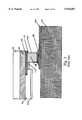
- This integrated circuitincludes a silicon (Si) based integrated circuit 101.
- Insulating film 102coats the underside of circuit 101 to protect and passivate it.
- Epoxy layer 103 and a silicon cap 104cover circuit 101.
- Epoxy layer 103 and silicon cap 104also cover metal bridge 105.
- Metal bridge 105electrically connects circuit 101 to silicon post 106.
- Epoxy section 111mechanically secures circuit 101, metal bridge 105 and silicon post 106.
- Nickel (Ni) plate 107covers silicon post 106 and forms a butt-joint with metal bridge 105.
- Nickel plate 107is electrically coupled to silicon post 106 and metal bridge 105.
- Nickel plate 107provides the integrated circuit with a connection point to external circuitry.
- This prior-art contactcomprises:
- circuit board conductor 109As illustrated in FIG. 1, the contact of the integrated circuit has been soldered to circuit board conductor 109 with solder fillet 108. Circuit board conductor 109 has been formed onto circuit board substrate 110.
- nickel plate 107covers the sidewalls of silicon post 106, which helps to strengthen the bond between the circuit 101 and the circuit board substrate 110. This is due to the fact that solder can be placed on nickel plate 107 on the sidewalls of silicon post 106 as illustrated in FIG. 1. It also facilitates inspection during surface mount of the integrated circuit to the circuit board. Whether a good mount is made can be easily confirmed by looking at the solder on the sidewalls of silicon post 106.
- nickel plate 107extends over the sidewalls of silicon post 106 and contacts the side of metal bridge 105, forming a butt-joint interface between nickel plate 107 and metal bridge 105. This provides for an electrical contact between circuit board conductor 109 and circuit 101.
- the physical surface of the side of metal bridge 105might not be flat enough to ensure a reliable bond at this butt-joint interface.
- the side of metal bridge 105is difficult to clean because of its location on the side of the wafer. The bond at this butt-joint interface therefore might be weakened if the side of metal bridge 105 is not flat or has not been thoroughly cleaned.
- this butt-joint interfacealso limits the materials that can be used for nickel plate 107 and metal bridge 105. This is so because metal bridge 105 and nickel plate 107 can comprise more than one metal layer.
- the bonding layer of nickel plate 107then has to be formed so as to bond with each metal layer at the side of metal bridge 105 in order to form an effective contact. Accordingly, the selection of materials that can be used for metal bridge 105 and for the bonding layer of nickel plate 107 is limited.
- FIG. 2shows a prior-art contact that avoids a butt-joint by using a wrap-around flange contact.
- Silicon based circuit 101, insulating film 102, epoxy layer 103, silicon cap 104, metal bridge 105, silicon post 106, solder filet 108, circuit board conductor 109, circuit board substrate 110, and epoxy section 111are similar to that of the above described butt-joint contact.
- wrap around nickel plate 112 and metal bridge 105have a horizontal flange interface 113. While the wrap around flange avoids the problems associated with a butt-joint, it is still a relatively complex design, requiring a rather involved series of processing steps and a relatively large amount of wafer area dedicated to contact fabrication.
- An object of the present inventionis to simplify the process of fabricating contacts for electronic devices.
- Another objectis to increase the simplicity and the reliability of contacts for electronic devices.
- a further objectis to increase the wafer packing density of an electronic circuit by reducing the substrate area that is used for fabricating the device's contacts.
- Another objectis to provide contacts that have physical and electronic properties applicable to varied types of electronic devices.
- a contact for an electronic devicecomprises a standoff on the bottom surface of the substrate and a lower wire that extends from the standoff to an upper wire that runs on an encapsulant protrusion.
- Such a contactis fabricated by forming a trench in the top surface of a substrate.
- the trenchmay be located near the edge of an electronic circuit or discrete component formed using or attached to the substrate.
- an insulation layeris formed that has a through hole at a connection point within the circuit or component, and that ends part way through the trench.
- An upper wireis formed that runs from the connection point into the trench.
- the top of the substrateis encapsulated, forming an encapsulant protrusion in the trench.
- the substrateis selectively thinned from the bottom, exposing part of the bottom surface of the upper wire.
- a standoffis formed below the bottom surface of the substrate.
- the standoffcan be formed from the substrate during the selective thinning step.
- a lower wireis formed that runs on the bottom of the substrate from the exposed portion of the upper wire and onto the standoff.
- the trench in which the upper wires and the lower wires connectis formed from the bottom of the substrate after it has been encapsulated.
- the thinning of the substrate's bottom surfaceleaves a portion of the bottom surface of the substrate substantially co-planar with the bottom of the contacts.
- FIG. 1illustrates a cross-sectional side view of a prior-art integrated circuit butt-joint contact has been soldered onto a circuit board.
- FIG. 2illustrates a cross-sectional side view of a prior-art integrated circuit wrap-around flange contact that has been soldered onto a circuit board.
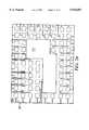
- FIGS. 3 and 3billustrate a top view of a substrate wafer showing how its top surface is tiled with replications of die, each of which will become an electronic device, and a cross-sectional side view of a portion of the wafer showing the electronic circuit or component areas for two adjacent devices, each having a connection point.
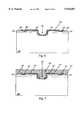
- FIG. 4shows a cross-sectional side view of the wafer portion of the previous Figure after a trench has been etched in the wafer between the two electronic circuit areas.
- FIG. 5shows a cross-sectional side view of the wafer portion of the previous Figure after an insulator has been formed on selected portions of the top of the wafer according to a pattern.
- FIG. 6shows a cross-sectional side view of the wafer portion of the previous Figure after a gold wire has been formed on top of the wafer and the insulator.
- FIG. 7shows a cross-sectional side view of the wafer portion of the previous Figure after a relatively thick layer of epoxy has been applied to the top surface of the wafer, the insulator, and the gold wire, which encapsulates them into a strong and rigid unit and which forms an encapsulant protrusion.
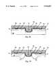
- FIG. 8shows a cross-sectional side view of the wafer portion of the previous Figure after the wafer has been thinned from the bottom to form the bottom surface of the electronic device.
- FIG. 9shows a cross-sectional side view of the wafer portion of the previous Figure after selected portions of the wafer's bottom have been further thinned, which exposes the gold wire at the bottom of the protruding encapsulant.
- FIG. 10shows a cross-sectional side view of the wafer portion of the previous Figure after epoxy standoffs have been placed on the bottom surface of wafer.
- FIG. 11shows a cross-sectional side view of the wafer portion of the previous Figure after an insulator has been formed on its bottom according to a pattern.
- FIG. 12shows a cross-sectional side view of the wafer portion of the previous Figure after a contact wire has been formed on its bottom surface.
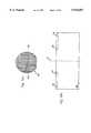
- FIGS. 13 and 13bshow a cross-sectional side view of the wafer portion of the previous Figure after it has been sawed into electronic devices, each with an attached contact and a corresponding partial bottom view of the same two electronic devices, each with multiple contacts in a two dimensional array.
- FIG. 14shows a cross-sectional side view of the electronic device and contact of the previous Figure after it has been soldered onto a circuit board.
- FIG. 15show a complete bottom view of one of the electronic devices of the previous Figure, with multiple contacts in a two dimensional array and with a bottom substrate surface that drops down to circuit-board level to dissipate heat generate in the electronic device by transferring the heat to the circuit board.
- FIG. 16shows a cross-sectional side view of the electronic device, contact and drop bottom of the previous Figure after being soldered onto a circuit board.
- FIGS. 17a and 17billustrates a cross-sectional side view of two electronic devices and contacts comparable to those of FIG. 13, but made using a gallium arsenide substrate wafer for which no insulator is necessary.
- FIG. 18illustrates a cross-sectional side view according to an alternative method which the wafer portion of FIG. 7 is next thinned from the bottom to form the bottom surface of substrate posts.
- FIG. 19shows a cross-sectional side view of the wafer portion of the previous Figure after selected portions of it have been further thinned, which exposes the bottom of the gold wire and which forms the substrate posts.
- FIG. 20shows a cross-sectional side view of the wafer portion of the previous Figure after an insulator has been formed on the bottom of the wafer according to a pattern.
- FIG. 21shows a cross-sectional side view of the wafer portion of the previous Figure after a contact wire has been formed on the bottom of the wafer.
- FIGS. 22a and 22bshow a cross-sectional side view of the wafer portion of the previous Figure after it has been sawed into two electronic devices each with an attached contact and a corresponding partial bottom view of these same two electronic devices, each with multiple contacts in a two dimensional array.
- FIGS. 23a and 23bshow a cross-sectional side view of two electronic devices and contacts comparable to those of the previous Figure, but made using a gallium arsenide substrate wafer for which no insulator is necessary.
- FIG. 24shows a complete bottom view of the electronic device of the previous Figure, with multiple contacts in a two dimensional array and with a bottom substrate surface that drops down, according to an irregular shape, to circuit-board level to transfer heat generated in the electronic device to the circuit board.
- FIG. 25illustrates a cross-sectional side view according to an alternative method in which the wafer portion of FIG. 3 next has an insulator formed on selected portions of its top surface according to a pattern.
- FIG. 26shows a cross-sectional side view of the wafer portion of the previous Figure after a gold wire has been formed on top of the wafer and the insulator.
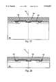
- FIG. 27shows a cross-sectional side view of the wafer portion of the previous Figure after a relatively thick layer of epoxy has been applied to the top of the wafer, the insulator, and the gold wire, which encapsulates them into a strong and rigid unit.
- FIG. 28shows a cross-sectional side view of the wafer portion of the previous Figure after it has been thinned from the bottom to form the bottom surface of substrate posts.
- FIG. 29shows a cross-sectional side view of the wafer portion of the previous Figure after a notch has been cut in its bottom surface between adjacent electronic circuits.
- FIG. 30shows a cross-sectional side view of the wafer portion of the previous Figure after it has been further thinned selectively from the bottom, which separates the substrate regions of adjacent electronic circuits and which forms the silicon posts.
- FIG. 31shows a cross-sectional side view of the wafer portion of the previous Figure after an insulator has been formed on the bottom of the wafer according to a pattern.
- FIG. 32shows a cross-sectional side view of the wafer portion of the previous Figure after contact wires have been formed on the bottom of the wafer according to a pattern.
- FIGS. 33a and 33bshow a cross-sectional side view of the wafer portion of the previous Figure after it has been sawed into two electronic devices each with an attached contact and corresponding partial bottom view of the same two electronic devices, each with multiple contacts in a two dimensional array.
- FIG. 34shows a complete bottom view of one of the electronic devices of the previous Figure, with multiple contacts in a two dimensional array and with a bottom substrate surface that drops down in a ribbed pattern to circuit-board level to transfer heat generated in the electronic device to the circuit board.
- FIG. 35shows a cross-sectional side view of two electronic devices and contacts comparable to those of FIGS. 33, but made using a gallium arsenide substrate wafer for which no insulator is necessary.
- FIGS. 36a and 36bshow a cross-sectional side view of two electronic devices and contacts comparable to those of the previous Figure and of FIG. 33, but made with epoxy standoffs on a gallium arsenide substrate.
- FIG. 37shows a complete bottom view of one of the electronic devices of the previous Figure, with multiple contacts in a two dimensional array and with a bottom substrate surface that drops down, in a pillared pattern, to circuit-board level to transfer heat generated in the electronic device to the circuit board.
- the present inventionencompasses embodiments involving various types of contacts for electrical or electronic devices that include a contact layer or wire that runs on the bottom surface of an insulative standoff located on the bottom surface of the devices' substrate underneath the passive or active circuit or component of an electronic device (i.e. the die).
- the present inventionalso encompasses embodiments in which there is no insulative standoff, wherein the contact layer runs over a substrate standoff.
- One embodimentemploys a trench within the top surface of the substrate to connect the contact layer to an upper wire or beam that runs to the circuit or component on the die and where another embodiment uses a bottom-surface trench.
- Yet another embodimentincorporates insulative substrates and another uses conductive substrates with insulation layers.
- Still another embodimentuses a drop bottom, in which the substrate extends down to the circuit board to which the device is attached, so as to transfer heat thereto.
- Die-bottom contactscomprising a standoff that is applied to the bottom surface of the substrate, a wire running on the standoff and an insulation layer between the wire and the substrate are illustrated in FIG. 13, FIG. 15 and FIG. 17. How such a contact is attached to a circuit board is illustrated in FIG. 14 and FIG. 16. How such a contact is fabricated is illustrated in FIG. 3 through FIG. 13. During fabrication, a wafer is typically held by a carrier.
- a trenchis formed in the top surface of a substrate, such as, but not limited to, a semiconductor wafer.
- the trenchmay be located near the edge of an electronic circuit or component, such as, but not limited to, an integrated circuit.
- the circuit or componentis formed using the substrate, or is attached to the substrate.
- An upper insulation layeris formed having a through-hole over a connection point within the circuit.
- the insulation layerends part way through the trench.
- the top of the substrateis encapsulated, forming an encapsulant protrusion in the trench.
- the encapsulantcan include a cap layer.
- the substrateis thinned from the bottom, thus forming the bottom surface of the finished electronic device.
- the substrateis further selectively thinned from the bottom to expose part of the bottom surface of the upper wire on the encapsulant protrusion.
- a standoffis applied to or formed on the bottom surface of the substrate.
- a lower insulation layeris formed that has a through hole over the exposed portion of the upper wire.
- a lower wire or contact layeris formed that runs on the bottom surface of the substrate from the exposed portion of the upper wire and onto the standoff.
- the top surface of the electronic devicescan be marked, so as to identify the part type and the orientation of pin number 1.
- the waferis diced. For some embodiments, this completes the fabrication of the electronic device.
- the electronic devicescan be tested while still attached to a carrier.
- FIG. 3illustrates a top view of substrate wafer 300, with a corresponding cross section.
- the top surface of substrate wafer 300has been used to fabricate a number of integrated circuits each within a rectangular die that is replicated or tiled across the wafer.
- Cut line or separation plane 311is one of the planes along which substrate wafer 300 will be separated or diced into individual electronic devices--finished electronic devices, not merely die requiring a subsequent assembly process.
- substrate wafer 300is formed of crystalline silicon (Si).
- substrate wafer 300is formed of crystalline silicon (Si).
- Other embodimentsuse other semiconductors for substrate wafer 300 such as but not limited to the following: gallium arsenide (GaAs), silicon germanium (SiGe), silicon carbide (SiC), gallium phosphide (GaP) or the like.
- insulative substratessuch as, but not limited to ceramic materials, sapphire, quartz or the like.
- a cross-sectional view of substrate wafer 300is also shown in FIG. 3, the cross section being taken along line 3(b).
- the top surface of substrate wafer 300has been used to fabricate an integrated circuit within electronic circuit regions 301.
- Electronic circuit regions 301include connection points 302. An electrical signal or power supply voltage must be connected between connection points 302 and circuitry external to the finished electronic device in order for it to operate properly.
- electronic circuit regions 301suggest an integrated circuit that is fabricated using the top surface of substrate wafer 300. Nevertheless, the techniques and embodiments described throughout this disclosure apply to contacts for any electronic circuit or discrete electronic component that can be fabricated using, or attached to, substrate wafer 300.
- a passive discrete componentsuch as, but not limited to a resistor or capacitor, or an active discrete component such as, but not limited to a transistor, power transistor, diode, thrysister, field-effect transistor (FET) or the like could include connection points 302 and could have contacts fabricated according to any of the techniques or embodiments disclosed herein.
- FETfield-effect transistor
- various integrated circuits or other electronic circuitscould be attached to substrate wafers 300 could include connection points 302 and could then have contacts fabricated according to any of the techniques or embodiments disclosed herein.
- an electronic circuitis formed within or attached to square or rectangular shaped electronic regions 301 that are replicated both horizontally and vertically, covering the top surface of substrate wafer 300. Edges of two adjacent electronic circuit regions 301 are also shown in FIG. 3. Connection points 302 are typically near those edges, but could be located away from the edge if desired.
- a potential advantage of the present method of fabricating contactsis higher wafer packing density. That is, the area of substrate wafer 300 that must be dedicated to forming contacts might be reduced over that required, for example, in the prior-art contact shown in FIG. 2. This may allow more replications of electronic circuit regions 301 to fit on a wafer, thus reducing the manufacturing cost for each device.
- the first step in fabricating a contact with a substrate postis to form a trench in substrate wafer 300 near, and possibly parallel to, an edge of electronic circuit regions 301.
- Trench 303can be formed by any technique, such as but not limited to wet chemical etching, dry plasma etching, mechanical micro machining, sawing, diamond-tip sawing or the like. It might be advantageous to use a technique that allows a relatively deep but narrow trench to be formed, such as but not limited to cutting a starter trench with a diamond-tip saw and then etching, using etching techniques and specialized equipment designed for deep narrow trenches, or the like.
- Trench 303is a relatively deep recess (150 microns deep, for example) into substrate wafer 300. As will become clear, trench 303 must be formed deeper than the thickness of the substrate that will remain beneath electronic circuit region 301 in the finished device.
- trench 303 of a suitable size and shapeNumerous methods of forming trench 303 of a suitable size and shape are known.
- the regions of substrate wafer 300 that are not to be etchedcan be protected by a photolithographic chemical resist and etch process as follows:
- a maskcan be prepared on a glass plate.
- the maskdetermines which areas of substrate wafer 300 are to be protected.
- Substrate wafer 300is coated with a photosensitive resist layer, then ultraviolet light is projected onto the regions that are to be etched (or that are not to be etched).
- the resulting substrate wafer 300is subjected to a resist-developer chemical solution that removes only the regions of the resist that were exposed to the ultraviolet light (or that were not exposed to the ultraviolet light).
- a chemical etch solutionis applied that etches substrate wafer 300 in those regions not protected by the resist. After etching has occurred to the desired depth and width, the resist is removed by a resist-dissolving solution.
- dry plasma or ion etching processescan be used instead of the above described wet chemical etch process.
- therecan be a photosensitive layer applied and developed on top of a non-photosensitive resist layer, which is then selectively removed prior to the etch process. Any method of forming trench 303 of a suitable size and shape can be employed.
- insulation layer 304(with a thickness of 25 microns or less, for example) on selected regions of substrate wafer 300. Insulation layer 304 is formed in a pattern such that connection points 302 and a portion of trench 303 are not insulated.
- insulation layer 304directly on top of substrate wafer 300.
- insulation layer 304is separated from substrate wafer 300 by other layers (not shown) that form the electronic circuit.
- layerscan include, but are not limited to interconnect layers, insulation layers or the like.
- insulation layer 304serves as the passivation layer over electronic circuit regions 301.
- Insulation layer 304can be formed by any technique that selectively forms regions of an insulation layer on top of a substrate according to a pattern.
- Any technique for forming a layer of any insulating material on top of substrate wafer 300can be used, such as but not limited to the following: silicon oxide grown from a silicon substrate wafer by an oxidation process (at least for those regions where the substrate is exposed); or silicon oxide (SiO 2 ) or silicon (nitride (Si 3 N 4 ), aluminum oxide (Al 2 O 3 ), polymide resins, epoxy, acrylics, patternable plastics deposited on top of substrate wafer 300; or the like.
- Any technique for selectively removing regions of that insulation layercan be used, such as, but not limited to a photolithographic etch processes, photolithography directly on a photosensitive insulator, or the like.
- Interconnection wire 305extends from connection points 302 within electronic circuit regions 301 into the non-insulated portion of trench 303. Any technique of forming interconnection wire 305 can be used, such as but not limited to pattern plating, sputter deposition of a metal layer within a low-pressure insert gas followed by photo-lithographically selective etching of that layer, or the like.
- Interconnection wire 305can be any substance of suitable conductivity, for example a metal, such as but not limited to gold (Au), silver (Ag), copper (Cu), aluminum (Al), nickel (Ni), alloys thereof or layers thereof.
- a metalsuch as but not limited to gold (Au), silver (Ag), copper (Cu), aluminum (Al), nickel (Ni), alloys thereof or layers thereof.
- Interconnection wire 305 as well as the other metal, wire, interconnect or contact layers described hereinmight be advantageously formed of layers of metals, such as but not limited to the following: a thin barrier metal layer (as can allow current to flow between certain metals while avoiding the metals directly touching) or a thin seed metal layer (as can facilitate forming a metal layer by plating); followed by a main layer; followed by a gold flash layer (as can resist corrosion).
- a thin barrier metal layeras can allow current to flow between certain metals while avoiding the metals directly touching
- a thin seed metal layeras can facilitate forming a metal layer by plating
- main layerfollowed by a gold flash layer (as can resist corrosion).
- the next step in forming a contactis to encapsulate substrate wafer 300, insulating layer 304 and interconnection wire 305.
- the top surfaces of these structuresare covered with a relatively thick layer (150 microns, for example) of a strong and insulative encapsulant.
- the encapsulantfills trench 303, thus forming encapsulant protrusion 313.
- Encapsulant layer 306can be formed of epoxy, glass, plastic, polymide resins, Teflon®, silicon oxide (SiO 2 ), silicon nitride (Si 3 N 4 ), mixtures thereof, layers thereof, or any other material that is non-conducting, relatively rigid and strong, and sufficiently flexible or compliant to allow for thermal expansion both in subsequent wafer processing and in the complete electronic system.
- Encapsulant layer 306can be formed of a material with thermal expansion characteristics similar to those of substrate wafer 300.
- Encapsulant layer 306can be applied using a variety of techniques. These techniques may attempt to keep encapsulant layer 306 at a uniform thickness, or to eliminate air bubbles within encapsulant layer 306 or between it and substrate wafer 300, insulating layer 304 and interconnection wire 305. In some embodiments, substrate wafer 300 is spun, possibly in a centrifuge, to form encapsulant layer 306. In alternative embodiments, encapsulant layer 306 comprises a high-temperature insulative epoxy material that is cured in a furnace.
- encapsulant layer 306can include a top or cap layer (not shown) containing materials, such as but not limited to the following: silicon, polysilicon, amorphous silicon, plastic, glass, epoxy, aluminum, diamond, mixtures thereof, layers thereof, or any other material that is relatively rigid and strong.
- This cap layercan make the finished electronic device more mechanically rugged. It can also serve as a thermal conduit to dissipate heat produced by the operating electronic device. This cap layer need not be an insulator.
- the next step in fabricating a contactis to remove material from the bottom surface of substrate wafer 300 so as to reduce its thickness.
- Any method of removing substrate material from the back of substrate wafer 300can be used, such as but not limited to back planing, back lapping, sandblasting, grinding, wet chemical etching, dry plasma etching or the like.
- the thickness remaining of substrate wafer 300determines the substrate thickness in the finished device (for example, 100 microns).
- the next stepis to selectively remove material from the bottom surface of substrate wafer 300 so as to reduce (by 2 microns, for example) its substrate thickness over encapsulant protrusion 313.
- Any method of selectively removing substrate material from the back of substrate wafer 300can be used, such as but not limited to the following: photo-lithographically selective wet chemical etching; photo-lithographically selective dry plasma; ion etching; or the like.
- the thinning steps of FIG. 8 and FIG. 9could be combined into a single step.
- Standoffs 320can be formed of a relatively thick layer (50 microns, for example) of a strong material such as epoxy, glass, plastic, polymide resins, Teflon®, silicon oxide (SiO 2 ), silicon nitride (Si 3 N 4 ), mixtures thereof, layers thereof, or any other material that is relatively rigid and strong, and sufficiently flexible or compliant to allow for thermal expansion both in subsequent wafer processing and in the complete electronic system.
- a strong materialsuch as epoxy, glass, plastic, polymide resins, Teflon®, silicon oxide (SiO 2 ), silicon nitride (Si 3 N 4 ), mixtures thereof, layers thereof, or any other material that is relatively rigid and strong, and sufficiently flexible or compliant to allow for thermal expansion both in subsequent wafer processing and in the complete electronic system.
- Hysol® FP4650 epoxymanufactured by Dexter Corp., Electronic Materials Division, of Industry, California, might be suitable for standoffs 320.
- standoffs 320can be formed of a
- Standoffs 320can be applied using a variety of techniques. These techniques may attempt to keep standoffs 320 at a uniform thickness, or to eliminate air bubbles within standoffs 320 or between it and substrate wafer 300.
- substrate wafer 300has standoffs 320 applied to its bottom surface in a screening process or the like is used in which a screen or mask allows an epoxy material to contact the bottom surface of substrate wafer 300 only at those locations where a standoff 320 is to be formed.
- substrate wafer 300has epoxy standoffs 320 applied to its bottom surface from a flexible disk or strip on which the standoffs have been pre-located at the appropriate positions.
- the next step in fabricating a contactis to form lower insulation layer 321 on the bottom surface of substrate wafer 300 according to a pattern.
- Lower insulation layer 321must not cover at least a portion of the part of interconnect layer 305 that is exposed on the bottom of the wafer. If substrate 300 is conductive, then lower insulation layer 321 must insulate substrate 300 from contact layer 307, discussed below in connection with FIG. 12, which is formed in the next step. It may be advantageous to have lower insulation layer 321 completely cover standoffs 320 in order to facilitate forming or increase the reliability of contact layer 307.
- the next step in fabricating a contactis to selectively form lower wires, lead wires or contact layer 307 (6 to 10 microns thick, for example) on the bottom surface of substrate wafer 300.
- One portion relative to each finished device, of contact layer 307connects with the exposed portion of interconnection wire 305.
- the other ends of contact layer 307runs onto standoffs 320 and optionally extends over their bottom surface, thus forming the bottom of each contact being fabricated.
- Contact layer 307completely covers standoffs 320 and extends beyond them toward the center of each electronic device. Such a large contact surface is optional, thus contact layer 307 may end at the inside edge of standoff 320, or it may only partially cover its bottom surface.
- Contact layer 307is formed from a metal or other conductor that facilitates connecting the contacts of the electronic device with the wiring on the surface to which the device is mounted.
- contact layer 307can be made of an easily solderable conductor such as but not limited to the following: nickel (Ni), nichrome-gold, nichrome-nickel, nickel-arsenic-gold, nickel-arsenic, nickel-gold, gold-tin-oxide (ATO), palladium-silicide, titanium (Ti), tungsten (W), titanium-tungsten (Ti-W), indium titanium oxide (ITO), aluminum (Al), copper (Cu), platinum (Pt), alloys thereof or layers thereof.
- Gold (Au) or silver (Ag)can also be used for contact layer 307.
- Pattern platingis not wasteful of materials and can be faster than, and result in a higher quality contact layer 307 than would result from depositing contact layer 307 by evaporation or sputtering.
- a first layer(0.2 microns thick, for example) of titanium-tungsten (Ti-W) is deposited on the bottom of substrate wafer 300.
- a second layer(0.2 microns thick, for example) of gold (Au) is deposited over the first layer.
- the second layeris then selectively coated by a photo resist layer (6 to 10 microns thick, for example) in the regions where contact layer 307 is not to be formed. Electroplating is then used to form a contact layer 307, which can actually become thicker than the photoresist layer.
- the photoresist layeris then stripped off and the first and second layers are etched away where they are not protected by contact layer 307.
- the contact's bottom surface dimensionscan vary from contact to contact. It is not necessary for any contact to have the same width or the same length as any other contact.
- the inter-contact pitchcan be variable.
- the contact's surface areaFor some uses of some types of electronic devices, it potentially is a significant advantage to be able to vary the contact's surface area. In the absence of this ability, if the current carrying capacity of a single contact is exceeded, then multiple contacts must be dedicated to carry the same signal or power-supply voltage level. Also, the ability to vary the contact's surface area might help reduce parasitic circuit elements such as resistance and inductance that can be introduced by a contact. Such a reduction could be a significant advantage in some cases, such as for power switching devices.
- the top surface of the electronic devicescan be marked while the devices are still attached to the wafer, so as to identify such information as the part type and the orientation of pin number 1.
- a screening process or the likecan be used for that marking.
- the electronic devices described throughout this disclosurecould possibly be tested while still in wafer form just prior to, or during, a final separation step. If the operation of each device is not affected by its contacts being still connected to those of the adjacent devices, then testing of each electronic device could possibly occur just prior to their being separated into individual devices. It is more common however, to cut and separate the devices before testing.
- the device separation and testingcan occur in three steps:
- testing while still on the wafermight provide significant cost savings over prior-art techniques, in which typically a wafer is tested and any defective dies within the wafer are marked, then the non-marked dies are assembled into packaged devices, and then the packaged devices are then tested a second time.
- the packaged devicescan be tested after being separated from the wafer without any wafer testing. If the yield of the wafer is high enough, the wafer testing step might be unnecessary--even if the bad devices were marked it may not be feasible to sort out the good devices for processing that differs from the processing of the bad devices.
- the final step in forming a contactis to separate substrate wafer 300 into individual electronic devices.
- This separationcan be achieved by any method, such as but not limited to sawing, etching, or the like.
- the separation formed by that sawing or etchingforms the outside surface of the finished electronic device.
- the electronic deviceis now completely packaged, unlike those prior-art techniques in which wafers are separated into dies, which are subsequently assembled into packaged devices.
- additional test or marking stepsmight be required.
- additional device assembly stepsmight be required in embodiments where contacts on the bottom of the device as disclosed herein are combined with additional contacts on the top of the device that are fabricated using other techniques.
- contacts as disclosed hereincan be combined in the same electronic device with top-side connections.
- FIG. 13a bottom view is also shown of the same electronic device, which is a cross section view taken along line 13(a).
- the cross sectionexposes a portion of the multiple rows of contacts is shown along each edge of the electronic device. As shown, there are only a few contacts in each row of the electronic device. In practice, there would be many such contacts in each row and more than one row of contacts on each edge. With variable sized contacts, the contacts may not line up in rows.
- a square package with sides of 7.5 millimeters in lengthcould include a total of 300 contacts along its four edges using three contact rows per edge and a pitch of approximately 300 microns between contacts.
- a typical prior-art microprocessor having 200 contacts around the edges of a 38 millimeter square packagecould be packaged according to the above embodiment, using a relatively conservative inter-contact pitch of approximately 760 microns and only one row of contacts per edge.
- an advanced integrated circuit having 1000 contacts around the edges of a 38 millimeter square packagewould require an inter-contact pitch of approximately 300 microns using two rows along each edge, or an inter-contact pitch of 600 microns using 4 rows of contacts.
- inter-contact pitch of 300 micronsis straightforward to achieve using the above substrate post embodiment.
- the inter-contact pitch achievable in practiceis likely to be limited by circuit board considerations, not the contacts. It may be difficult to reliably fabricate circuit board conductor 109, as illustrated in FIG. 14, with less than 150 microns spacing between conductors that are less than 150 microns in width.
- the contact fabricatedcomprises standoff 320, bottom insulator layer 321 and contact layer 307.
- the relative simplicity of this contactmight help to minimize parasitic elements being introduced into the circuit in which the contact is used. For some uses of some types of devices, including but not limited to power-switching devices and the like, this might be a significant advantage.
- solder fillet 108provides both mechanical and electrical connection between the contact and the circuit board.
- Contacts disclosed hereinare suitable for connecting with a circuit board using a variety of techniques, such as but not limited to surface mount soldering, gold compression bonding, epoxy, conductive epoxy or the like.
- the contacts described throughout this disclosureare suitable for connection to a variety of apparatus, including but not limited to circuit boards, glass plates, or the like.
- Drop bottom 315is a protruding portion of substrate 300.
- Drop bottom 315is formed by selectively not thinning portions of the bottom of substrate 300 during the selective thinning step discussed above in connection with FIG. 9. This results in drop bottom 315 having a bottom surface approximately co-planar with the bottom of the contacts of the finished electronic device.
- the selective thinningprovides a stand off between the electronic device and the circuit board to which the device is attached in the region near the contacts.
- Drop bottom 315connects with the circuit board or other apparatus to which the electronic device is attached, so that heat can be transferred out of the electronic device and into the circuit board, where the heat might be more easily dissipated without overheating the device.
- drop bottom 315has a square bottom surface that forms a significant portion of the bottom surface of substrate 300.
- Drop bottom 315could have any shape and could cover more or less area depending on the heat dissipation needs of the electronic device and the heat absorption, transfer and dissipation characteristics of the circuit board or the like to which the device is mounted.
- both drop bottom 315 and the contact of the electronic devicecan be soldered to circuit board conductors 109 with solder filets 108.
- Solder filets 108provide both mechanical connection and heat conduction with drop bottom 315. If substrate 300 is conductive, then the circuit board connector 109 connected to drop bottom 315 should either be electrically isolated or be tied to the substrate voltage appropriate for the electronic device.
- the contactcomprises a standoff and a wire that extends onto the standoff.
- a relatively large trenchis formed in the top surface of a substrate, such as but not limited to a semiconductor wafer.
- the trenchmay be located near the edge of an electronic circuit or component, such as but not limited to an integrated circuit.
- the circuit or componentis formed using the substrate, or is attached to the substrate.
- An upper interconnection wire or beamis formed that runs from the connection point into the trench.
- the top of the substrateis encapsulated, thus forming an encapsulant protrusion in the trench.
- the encapsulantincludes a cap layer.
- the substrateis thinned from the bottom, thus forming the bottom surface of the finished electronic device.
- the substrateis further selectively thinned from the bottom, thus exposing part of the bottom surface of the upper wire on the encapsulant protrusion.
- a standoffis applied to or formed on the bottom surface of the substrate.
- a lower wire or contact layeris formed that runs on the bottom surface of the substrate from the exposed portion of the upper wire and onto the standoff.
- the top surface of the electronic devicesare marked, so as to identify the part type and the orientation of pin number 1.
- the waferis diced. For some embodiments, this completes the fabrication of the electronic device.
- the electronic devicesare tested while still attached to the carrier.
- Gallium arsenideis a semiconductor that, unlike silicon, does not significantly conduct electricity unless the gallium arsenide is doped.
- Patternable insulator layers 304 and 321are not needed in gallium arsenide embodiments, or in other embodiments where substrate wafer is made of an insulator, such as but not limited to sapphire, quartz or the like.
- the step of adding a pattemable insulator described above in reference to FIG. 5is not needed. Rather, interconnect wire 305 and contact layer 307 can be insulated from substrate wafer 300 by simply not doping the gallium arsenide substrate in the areas where there is to be no electrical conductivity.
- FIG. 17illustrates the contact that results in embodiments that use gallium arsenide as the substrate.
- a major difference in the contact shown in FIG. 17 from the contact of FIG. 13is that insulation layers 304 and 321 are missing.
- Connection point 310is formed by doping the gallium arsenide so that it becomes conductive at the point where interconnection wire 305 connects to it.
- the process required to produce a contact according to this insulative substrate embodimentis even simpler than that disclosed for conductive substrates. Such simplicity may result in advantages such as reduced cost and higher yield. Also, the resulting contact has even fewer elements than for conductive substrates, which may help improve the reliability of the contact.
- FIG. 22A contact comprising a substrate standoff, a wire that runs onto it and an insulation layer formed there between is shown in FIG. 22.
- An example of how such contacts are fabricatedis shown in FIG. 3 though FIG. 7 and FIG. 18 though FIG. 22.
- FIG. 3 through FIG. 7 and the steps and materials they represent and involveare discussed in more detail above.
- a relatively large trenchis formed in the top surface of a substrate, such as but not limited to a semiconductor wafer.
- the trenchmay be located near the edge of an electronic circuit or component, such as but not limited to an integrated circuit.
- the circuit or componentis formed using the substrate, or is attached to the substrate.
- An upper insulation layeris formed that has a through hole over a connection point within the circuit.
- the insulation layerends part way through the trench.
- the top of the substrateis encapsulated, thus forming an encapsulant protrusion in the trench.
- the encapsulantincludes a cap layer.
- the substrateis thinned from the bottom, thus forming the bottom surface of the substrate standoff.
- the substrateis further selectively thinned from the bottom, thus exposing part of the bottom surface of the upper wire on the encapsulant protrusion and forming the sidewalls of the substrate standoff.
- a lower insulation layeris formed that has a through hole over the exposed portion of the upper wire.
- a lower wire or contact layeris formed that runs on the bottom surface of the substrate from the exposed portion of the upper wire and onto the standoff.
- the top surface of the electronic devicesare marked, so as to identify the part type and the orientation of pin number 1.
- the waferis diced. For some embodiments, this completes the fabrication of the electronic device.
- the electronic devicesare tested while still attached to a carrier.
- the next step in fabricating a contactis to take substrate wafer 300, as shown in FIG. 7, and remove material from its bottom surface so as to reduce its thickness.
- Any method of removing substrate material from the back of substrate wafer 300can be used, such as but not limited to back planing, back lapping, sandblasting, grinding, wet chemical etching, dry plasma etching or the like.
- the thickness remaining of substrate wafer 300determines the height of the substrate standoff in the contact in the finished device. For example, thinning the substrate wafer to a thickness of 150 microns allows a substrate thickness of 100 microns in the finished packaged device and a 50 micron standoff between the bottom surface of the contacts and the bottom surface of the device.
- the next stepis to selectively remove material from the bottom surface of substrate wafer 300 so as to reduce its substrate thickness over encapsulant protrusion 313 and so as to form the sidewalls of substrate standoffs 325 similar to drop bottoms 315 of FIGS. 15 and 16.
- Any method of selectively removing substrate material from the back of substrate wafer 300can be used, such as but not limited to the following: photo-lithographically selective wet chemical etching; photo-lithographically selective dry plasma; ion etching; or the like.
- the thinning steps of FIG. 18 and FIG. 19could be combined into a single step.
- the next step in fabricating a contactis to form lower insulation layer 321 on the bottom surface of substrate wafer 300 according to a pattern.
- Lower insulation layer 321is discussed above in reference to FIG. 11.
- the next step in fabricating a contactis to form lower wire or contact layer 307 on the bottom surface of substrate wafer 300 according to a pattern.
- Contact layer 307is discussed above in connection with FIG. 12.
- FIG. 22illustrates a cross sectional side view of the wafer of the previous Figure after being sawed, etched, or otherwise separated into two finished devices, each with an attached contact.
- FIG. 22also shows a partial bottom view of the same two devices of the previous Figure, the previous Figure being a cross section view taken along line 22(aa). Each device has multiple contacts arranged in multiple rows along each edge of the device.
- the electronic deviceis now completely packaged, unlike those prior-art techniques in which wafers are separated into dies, which are subsequently assembled into packaged devices.
- additional test or marking stepsmight be required.
- additional device assembly stepsmight be required in embodiments where contacts on the bottom of the device as disclosed herein are combined with additional contacts on the top of the device that are fabricated using other techniques.
- contacts as disclosed hereincan be combined in the same electronic device with top-side connections.
- FIG. 23 and FIG. 24A contact for an electronic device using an insulative substrate is illustrated in FIG. 23 and FIG. 24.
- the contactcomprises a substrate standoff and a contact layer or lower wire that extends onto the standoff.
- a relatively large trenchis formed in the top surface of a substrate, such as but not limited to a semiconductor wafer.
- the trenchmay be located near the edge of an electronic circuit or component, such as but not limited to an integrated circuit.
- the circuit or componentis formed using the substrate, or is attached to the substrate.
- An upper interconnection wire or beamis formed that runs from the connection point into the trench.
- the top of the substrateis encapsulated, thus forming an encapsulant protrusion in the trench.
- the encapsulantincludes a cap layer.
- the substrateis thinned from the bottom, thus forming the bottom surface of the finished electronic device.
- the substrateis further selectively thinned from the bottom, thus exposing part of the bottom surface of the upper wire on the encapsulant protrusion and forming the substrate standoff.
- a lower wire or contact layeris formed that runs on the bottom surface of the substrate from the exposed portion of the upper wire and onto the standoff.
- the top surface of the electronic devicesare marked, so as to identify the part type and the orientation of pin number 1.
- the waferis diced. For some embodiments, this completes the fabrication of the electronic device.
- the electronic devicesare tested while still attached to a carrier.
- Gallium arsenideis a semiconductor that, unlike silicon, does not significantly conduct electricity unless the gallium arsenide is doped.
- Pattemable insulator layers 304 and 321are not needed in gallium arsenide embodiments, or in other embodiments where substrate wafer is made of an insulator, such as but not limited to sapphire, quartz or the like. Also, the steps of adding patternable insulators described above in reference to FIG. 5 and FIG. 20 are not needed. Rather, interconnect wire 305 and contact layer 307 can be insulated from substrate wafer 300 by simply not doping the gallium arsenide substrate in the areas where there is to be no electrical conductivity.
- FIG. 23illustrates the contact that results in embodiments that use gallium arsenide as the substrate.
- a major difference from the contact of FIG. 22is that insulation layers 304 and 321 are missing.
- Connection point 310is formed by doping the gallium arsenide so that it becomes conductive at the point where interconnection wire 305 connects to it.
- the process required to produce a contact according to this insulative substrate embodimentis even simpler than that disclosed for conductive substrates. Such simplicity may result in advantages such as reduced cost and higher yield. Also, the resulting contact has even fewer elements than for conductive substrates, which may help improve the reliability of the contact.
- FIG. 24illustrates an electronic device similar to that of the previous Figure, except that it includes an irregularly shaped drop bottom 315.
- Drop bottom 315is a protruding portion of substrate 300. It has a bottom surface approximately co-planar with the bottom of the contacts of the finished electronic device. Drop bottom 315 is discussed above in connection with FIG. 15.
- drop bottom 315has an irregular shaped bottom surface, perhaps designed so that drop bottom 315 protrudes beneath those portions of the electronic circuit or device that produce substantial heat.
- Drop bottom 315could have any shape and could cover more or less area depending on the heat dissipation needs of the electronic device and the heat absorption, transfer and dissipation characteristics of the circuit board or other apparatus to which the device is mounted.
- FIG. 33 and FIG. 34A contact comprising a substrate standoff, a wire that runs onto it and an insulation layer there between is illustrated in FIG. 33 and FIG. 34. How such contacts are fabricated is shown in FIG. 3 and FIG. 25 though FIG. 34.
- An upper insulation layeris formed on the top surface of a substrate, such as but not limited to a semiconductor wafer.
- the circuit or component that will make up the finished electronic device(such as but not limited to an integrated circuit) is formed using the substrate, or is attached to the substrate.
- the upper insulation layerhas a through hole over a connection point within the circuit. Also, the insulation layer ends prior to the plane that will separate adjacent electronic devices.
- An upper interconnection wire or beamis formed that runs from the connection point to the separation plane.
- the top of the substrateis encapsulated.
- the encapsulantincludes a cap layer.
- the substrateis thinned from the bottom, thus forming the bottom surface of the substrate standoff.
- the substrateis further selectively thinned from the bottom, thus forming the sidewalls of the substrate standoff.
- This selective thinningalso forms a relatively large trench in the bottom surface of the substrate, thus exposing part of the bottom surface of the upper wire.
- This selective thinningmay be performed by first making a saw cut along the device separation plane and then etching.
- a lower insulation layeris formed that has a through hole over the exposed portion of the upper wire.
- a lower wire or contact layeris formed that runs on the bottom surface of the lower insulation layer from the exposed portion of the upper wire and onto the standoff.
- the top surface of the electronic devicesare marked, so as to identify the part type and the orientation of pin number 1.
- the waferis diced. For some embodiments, this completes the fabrication of the electronic device.
- the electronic devicesare tested while still attached to a carrier.
- the top of the wafer shown in FIG. 3is selectively coated with insulation layer 304.
- Insulation layer 304is discussed above in connection with FIG. 5.
- Interconnection wire 305extends from connection point 302 within electronic circuit region 301 into the non-insulated portion of trench 303 (for example, 6 to 10 microns thick and 10 microns wide, or a width going up to whatever is appropriate for the current carried). Interconnection wire 305 is discussed above in connection with FIG. 6.
- substrate wafer 300, insulating layer 304 and interconnection wire 305are encapsulated.
- the top surfaces of these structuresare covered with a relatively thick layer (150 microns, for example) of a strong and insulative encapsulant.
- Encapsulant layer 305is discussed above in connection with FIG. 7.
- substrate wafer 300then is thinned from its bottom surface so as to reduce its thickness.
- Any method of removing substrate material from the back of substrate wafer 300can be used, such as but not limited to back planing, back lapping, sandblasting, grinding, wet chemical etching, dry plasma etching or the like.
- the thickness remaining of substrate wafer 300determines the height of the substrate standoff in the contact in the finished device. For example, thinning the substrate wafer to a thickness of 150 microns allows a substrate thickness of 100 microns in the finished device and a 50 micron standoff between the bottom surface of the contacts and the bottom surface of the device.
- the next stepis to selectively remove material from the bottom surface of substrate wafer 300 so as to reduce its substrate thickness along separation plane 311.
- Any method of selectively removing substrate material from the back of substrate wafer 300can be used, such as but not limited to the following: diamond saw cutting, photo-lithographically selective wet chemical etching; photo-lithographically selective dry plasma; ion etching; or the like.
- first a diamond-shaped saw cutcan be made and then selective etching can be used to broaden the cut and to form the substrate standoffs.
- the thinning steps of FIG. 29 and FIG. 30could be combined into a single step.
- the top trench 303 shown first in FIG. 4 and again in FIG. 9can be accomplished using the same technique as that discussed above in relation to saw cut 340 shown in FIG. 29 and trench 352 shown in FIG. 31.
- the top trench 303could first be cut with the diamond-shaped saw cut such as saw-cut 340 of FIG. 29 to reduce its substrate thickness. Then, selective etching can be used to broaden trench 303 to the shape shown in FIG. 4.
- the bottom trench 350 shown in FIG. 9could be pre-cut in the same manner with the diamond-shaped saw and selectively etched to achieve the shape shown in FIG. 9.
- the next step in fabricating a contactis to form lower insulation layer 321 on the bottom surface of substrate wafer 300 according to a pattern.
- Lower insulation layer 321is discussed above in reference to FIG. 11.
- the next step in fabricating a contactis to form lower wire or contact layer 307 on the bottom surface of substrate wafer 300 according to a pattern.
- Contact layer 307is discussed above in connection with FIG. 12.
- the final step in fabricating a contactis to separate substrate wafer 300 into completed electronic devices, each with a set of attached contacts, as illustrated in FIG. 33.
- the separation formed by this sawing, etching or the likefinishes the formation of the contact.
- FIG. 33also shows a bottom view of the same two die of the previous Figure, the previous Figure being a cross section view taken along line 33(a). Each die has multiple rows of contacts along each edge.
- the electronic deviceis now completely packaged, unlike those prior-art techniques in which wafers are separated into dies, which are subsequently assembled into packaged devices. Alternatively, additional test or marking steps might be required.
- Drop bottoms 315are protruding portions of substrate 300. They are formed by selectively not thinning portions of the bottom of substrate portion 300 during at least part of the thinning step discussed in connection with FIG. 31. Drop bottoms 315 are discussed above in connection with FIG. 15, FIG. 16 and FIG. 24.
- a contactcomprising an insulative substrate standoff and a wire that runs onto it is shown in FIG. 35.
- An upper or interconnection wire or beamis formed on the top surface of a substrate, such as but not limited to a semiconductor wafer.
- the circuit or component that will make up the finished electronic device(such as but not limited to an integrated circuit) is formed using the substrate, or is attached to the substrate.
- the upper interconnection wireruns from a connection point within the circuit to the separation plane between devices.
- the top of the substrateis encapsulated.
- the encapsulantincludes a cap layer.
- the substrateis thinned from the bottom, thus forming the bottom surface of the substrate standoff.
- the substrateis further selectively thinned from the bottom, thus forming the sidewalls of the substrate standoff.
- This selective thinningforms a relatively large trench in the bottom surface of the substrate, thus exposing part of the bottom surface of the upper wire.
- This selective thinningmay be performed by first making a saw cut along the device separation plane and then etching.
- a lower wire or contact layeris formed that runs on the bottom surface of the lower insulation layer from the exposed portion of the upper wire and onto the standoff.
- the top surface of the electronic devicesare marked, so as to identify the part type and the orientation of pin number 1.
- the waferis diced. For some embodiments, this completes the fabrication of the electronic device.
- the electronic devicesare tested while still attached to a carrier.
- FIG. 35shows a contact according to embodiments that use an insulative substrate and die-bottom contacts on a substrate standoff.
- the major difference from the silicon-based, substrate-standoff contact of FIG. 33is that insulation layers 304 and 321 are missing.
- connection point 310is formed by doping the gallium arsenide so that it becomes conductive where it will electrically connect to interconnect wire 305.
- the process required to produce a contact according to this insulative substrate embodimentis even simpler than that disclosed for conductive substrates, which may result in advantages such as reduced cost and higher yield. Also, the resulting contact has even fewer elements than for conductive substrates, which may help improve the reliability of the contact.
- the relative simplicity of the contact of this embodimentmay help to minimize parasitic elements being introduced into the circuit in which the contact is used. For some uses of some types of devices, including but not limited to power-switching devices and the like, this may be a significant advantage.
- a contactcomprising a formed standoff and a wire that runs onto it is shown in FIG. 36.
- An upper or interconnection wire or beamis formed on the top surface of a substrate, such as but not limited to a semiconductor wafer.
- the circuit or component that will make up the finished electronic device(such as but not limited to an integrated circuit) is formed using the substrate, or is attached to the substrate.
- the upper interconnection wireruns from a connection point within the circuit to the separation plane between devices.
- the top of the substrateis encapsulated.
- the encapsulantincludes a cap layer.
- the substrateis thinned from the bottom, thus forming the bottom surface of the finished device.
- the substrateis further selectively thinned from the bottom, thus forming a relatively large trench in the bottom surface of the substrate, thus exposing part of the bottom surface of the upper wire.
- This selective thinningmay be performed by first making a saw cut along the device separation plane and then etching.
- a standoffis formed on the bottom surface of the wafer.
- a lower wire or contact layeris formed that runs on the bottom surface of the lower insulation layer from the exposed portion of the upper wire and onto the standoff.
- the top surface of the electronic devicesare marked, so as to identify the part type and the orientation of pin number 1.
- the waferis diced. For some embodiments, this completes the fabrication of the electronic device.
- the electronic devicesare tested while still attached to the carrier.
- FIG. 36shows a contact according to embodiments that use an insulative substrate and die-bottom contacts on a formed standoff.
- the major difference from the insulative-substrate, substrate-standoff contact of FIG. 35is that substrate standoff 325 is replaced with formed standoff 320.
- Formed standoff 320is discussed above in reference to FIG. 10.
- FIG. 37shows a complete bottom view of one of the electronic devices of the previous Figure, with multiple contacts in a two dimensional array and with a bottom substrate surface that drops down, in a pillared pattem, to circuit-board level.
- FIG. 15, FIG. 16, FIG. 24, FIG. 34; and FIG. 37show contact embodiments that include at least one drop bottom 315.
- Drop bottom 315is a protruding portion of substrate 300.
- Drop bottom 315has a bottom surface approximately co-planar with the bottom of the contacts of the finished electronic device.
- Drop bottom 315is formed by selectively not thinning portions of the bottom of substrate portion 300a during at least part of the thinning step that exposes the wire on the bottom of the encapsulant protrusion. Forming drop bottom 315 sometimes requires a first thinning step that forms the bottom surface of drop bottom 315, followed by a second selective thinning step that exposed the wire without further thinning drop bottom 315.
- Drop bottom 315mechanically connects with the circuit board, glass plate, or the like to which the electronic device is attached, so that heat can be transferred out of the electronic device and into the larger system, where the heat might be more easily dissipated without overheating the device.
- drop bottom 315can electrically connect to the circuit board and can be used to supply the substrate voltage or signal for the device.
- drop bottom 315can be employed with every type or embodiment of contact described herein.
- Drop bottom 315is been described herein as having a variety of shapes:
- Drop bottom 315could take on any shape including but limited to the above, horizontal ribs, vertical ribs, angled ribs, a single rib or wide strip down the middle of the device, combinations thereof and patterns thereof.
- the shape of drop bottom 315 and the number of drop bottoms 315 in a deviceare design alternatives that can be chosen taking into account the size of the electronic device, the heat generation characteristics of the electronic device, the heat absorption characteristics of the circuit board or other apparatus to which the electronic device is attached and the characteristics of the method of attaching the electronic device to the circuit board. For example, for a small device, a square or rectangle large enough to cover most of its bottom surface might be the simplest and most reliable, whereas for a large device such a drop bottom might introduce thermal expansion problems or solder flow problems that could be avoided by a ribbed or pillared drop bottom.
- Described hereinare several methods for fabricating several different types of contacts for electrical and electronic devices.
- the embodiments describedcan be employed in ways that potentially realize one or more significant advantages, including but not limited to short and simple fabrication processes, simple and reliable contacts, high wafer packing density, and contacts with advantageous physical and electronic properties that are applicable for use with varied types of electronic devices.
- an electronic devicecan be completely packaged using wafer fabrication processes, unlike those prior-art techniques in which wafers are separated into dies, which are subsequently assembled into packaged devices. Further, the finished electronic devices might be tested while still in wafer form. Alternatively, the finished devices might be tested after being separated, and the typical prior-art wafer testing step might be eliminated. Further, the processes disclosed for a contact with an insulative substrate, such as gallium arsenide, is even simpler than the processes disclosed for conductive substrates, such as silicon, which might further enhance these advantages.
- the contacts disclosed hereincan potentially be advantageously simple, mechanically rugged and sturdy, and contain relatively few elements. Thus, they might be inherently reliable. Further, the contacts disclosed using an insulative substrate, such as gallium arsenide, have even fewer elements compared to those described for conductive substrates, such as silicon, and thus might be even more inherently reliable.
- Wafer packing densitycan potentially be advantageously increased over those prior-art techniques that use substrate area to fabricate contacts. No substrate wafer area is dedicated to forming contacts; thus more replications of the electronic circuit or discrete component may fit on a wafer; thus manufacturing costs per device may be lower.
- the contacts disclosed hereincan potentially have advantageous physical properties, which may make them advantageously adaptable for use with electronic devices of different types.
- An inter-contact pitch compatible with 300-micron surface mount techniquesis easily achieved.
- the contact layercan be formed of an easily solderable material, or formed of gold, or formed of whatever material is suited for the particular mounting technique to be employed with the completed electronic device.
- Contacts formed on the bottom surface of the substrate as described hereinmight be combined in the same electronic device with contacts or pads on the top surface of the substrate; thus increasing the number of contacts per device and allowing flexibility in the types of contacts a device uses.
- the contacts disclosed hereincan potentially have advantageous electronic properties, which may make them advantageously adaptable for use with electronic devices of different types.
- the contact's bottom surface dimensions, both length and widthcan vary from contact to contact, which may reduce or eliminate the need to dedicate multiple contacts to carrying the a signal or a power supply voltage that requires substantial current. Both because of their varying sizes and because of their relative simplicity, the resulting contacts may help to minimize parasitic circuit effects, which may be advantageous for uses such as power switching devices and the like.
Landscapes
- Engineering & Computer Science (AREA)
- Computer Hardware Design (AREA)
- Microelectronics & Electronic Packaging (AREA)
- Power Engineering (AREA)
- Physics & Mathematics (AREA)
- Condensed Matter Physics & Semiconductors (AREA)
- General Physics & Mathematics (AREA)
- Manufacturing & Machinery (AREA)
- Internal Circuitry In Semiconductor Integrated Circuit Devices (AREA)
Abstract
Description
Claims (44)
Priority Applications (6)
| Application Number | Priority Date | Filing Date | Title |
|---|---|---|---|
| US08/788,762US5910687A (en) | 1997-01-24 | 1997-01-24 | Wafer fabrication of die-bottom contacts for electronic devices |
| GB9915640AGB2336034B (en) | 1997-01-24 | 1998-01-26 | Semiconductor wafer fabrication of die-bottom contacts for electronic devices |
| KR1019997006677AKR20000070442A (en) | 1997-01-24 | 1998-01-26 | Semiconductor water fabrication of die-bottom contacts for electronic devices |
| PCT/US1998/001541WO1998033215A1 (en) | 1997-01-24 | 1998-01-26 | Semiconductor wafer fabrication of die-bottom contacts for electronic devices |
| AU62512/98AAU6251298A (en) | 1997-01-24 | 1998-01-26 | Semiconductor wafer fabrication of die-bottom contacts for electronic devices |
| US09/105,504US6221751B1 (en) | 1997-01-24 | 1998-06-26 | Wafer fabrication of die-bottom contacts for electronic devices |
Applications Claiming Priority (1)
| Application Number | Priority Date | Filing Date | Title |
|---|---|---|---|
| US08/788,762US5910687A (en) | 1997-01-24 | 1997-01-24 | Wafer fabrication of die-bottom contacts for electronic devices |
Related Child Applications (1)
| Application Number | Title | Priority Date | Filing Date |
|---|---|---|---|
| US09/105,504DivisionUS6221751B1 (en) | 1997-01-24 | 1998-06-26 | Wafer fabrication of die-bottom contacts for electronic devices |
Publications (1)
| Publication Number | Publication Date |
|---|---|
| US5910687Atrue US5910687A (en) | 1999-06-08 |
Family
ID=25145469
Family Applications (2)
| Application Number | Title | Priority Date | Filing Date |
|---|---|---|---|
| US08/788,762Expired - LifetimeUS5910687A (en) | 1997-01-24 | 1997-01-24 | Wafer fabrication of die-bottom contacts for electronic devices |
| US09/105,504Expired - Fee RelatedUS6221751B1 (en) | 1997-01-24 | 1998-06-26 | Wafer fabrication of die-bottom contacts for electronic devices |
Family Applications After (1)
| Application Number | Title | Priority Date | Filing Date |
|---|---|---|---|
| US09/105,504Expired - Fee RelatedUS6221751B1 (en) | 1997-01-24 | 1998-06-26 | Wafer fabrication of die-bottom contacts for electronic devices |
Country Status (5)
| Country | Link |
|---|---|
| US (2) | US5910687A (en) |
| KR (1) | KR20000070442A (en) |
| AU (1) | AU6251298A (en) |
| GB (1) | GB2336034B (en) |
| WO (1) | WO1998033215A1 (en) |
Cited By (84)
| Publication number | Priority date | Publication date | Assignee | Title |
|---|---|---|---|---|
| WO2001003180A1 (en)* | 1999-07-01 | 2001-01-11 | Fraunhofer-Gesellschaft zur Förderung der angewandten Forschung e. V. | Method of subdividing a wafer |
| US6184465B1 (en)* | 1998-11-12 | 2001-02-06 | Micron Technology, Inc. | Semiconductor package |
| EP1073113A3 (en)* | 1999-07-26 | 2001-02-07 | STMicroelectronics, Inc. | Backside contact for touch sensing chip |
| US6187611B1 (en)* | 1998-10-23 | 2001-02-13 | Microsemi Microwave Products, Inc. | Monolithic surface mount semiconductor device and method for fabricating same |
| FR2802337A1 (en)* | 1999-12-14 | 2001-06-15 | St Microelectronics Sa | METHOD FOR INTERCONNECTING INTEGRATED CIRCUITS |
| US6291894B1 (en)* | 1998-08-31 | 2001-09-18 | Micron Technology, Inc. | Method and apparatus for a semiconductor package for vertical surface mounting |
| US6300670B1 (en) | 1999-07-26 | 2001-10-09 | Stmicroelectronics, Inc. | Backside bus vias |
| US6489557B2 (en) | 1999-08-30 | 2002-12-03 | Intel Corporation | Implementing micro BGA™ assembly techniques for small die |
| US20020185710A1 (en)* | 1999-09-13 | 2002-12-12 | Vishay Intertechnology, Inc. | Chip scale surface mount package for semiconductor device and process of fabricating the same |
| US6521513B1 (en)* | 2000-07-05 | 2003-02-18 | Eastman Kodak Company | Silicon wafer configuration and method for forming same |
| EP1085569A3 (en)* | 1999-09-13 | 2003-04-02 | Vishay Intertechnology, Inc. | Chip scale surface mount packages for semiconductor device and process of fabricating the same |
| FR2838578A1 (en)* | 2002-04-12 | 2003-10-17 | Thales Sa | INTERCONNECTION DEVICE FOR INTERFACE ACOUSTIC WAVE COMPONENTS |
| US6655022B1 (en) | 1998-09-24 | 2003-12-02 | Intel Corporation | Implementing micro BGA assembly techniques for small die |
| US20030230805A1 (en)* | 2002-04-23 | 2003-12-18 | Sanyo Electric Co., Ltd. | Semiconductor device and manufacturing method thereof |
| US20040017419A1 (en)* | 2002-07-29 | 2004-01-29 | Diane Lai | Method of forming a through-substrate interconnect |
| US6759688B2 (en) | 2001-11-21 | 2004-07-06 | Microsemi Microwave Products, Inc. | Monolithic surface mount optoelectronic device and method for fabricating the device |
| US6759275B1 (en)* | 2001-09-04 | 2004-07-06 | Megic Corporation | Method for making high-performance RF integrated circuits |
| US6777261B2 (en) | 2000-12-26 | 2004-08-17 | Micron Technology, Inc. | Method and apparatus for a semiconductor package for vertical surface mounting |
| US20040196137A1 (en)* | 2003-04-03 | 2004-10-07 | Ronald Dedert | Fuel tank resistor card having improved corrosion resistance |
| US20050017348A1 (en)* | 2003-02-25 | 2005-01-27 | Tessera, Inc. | Manufacture of mountable capped chips |
| US20050029668A1 (en)* | 2001-10-08 | 2005-02-10 | Micron Technology, Inc. | Apparatus and method for packaging circuits |
| US20050048695A1 (en)* | 2002-05-21 | 2005-03-03 | Micron Technology, Inc. | Super high density module with integrated wafer level packages |
| US20050104179A1 (en)* | 2003-07-03 | 2005-05-19 | Shellcase Ltd. | Methods and apparatus for packaging integrated circuit devices |
| US20050189637A1 (en)* | 2004-02-17 | 2005-09-01 | Sanyo Electric Co., Ltd. | Semiconductor device and manufacturing method thereof |
| US20050208703A1 (en)* | 1999-06-17 | 2005-09-22 | Infineon Technologies, Ag | Method of producing an electronic component with flexible bonding pads |
| US20050205977A1 (en)* | 2003-06-16 | 2005-09-22 | Shellcase Ltd. | Methods and apparatus for packaging integrated circuit devices |
| US20060087042A1 (en)* | 2004-10-26 | 2006-04-27 | Sanyo Electric Co., Ltd. | Semiconductor device and manufacturing method of the same |
| US20060094165A1 (en)* | 2004-10-29 | 2006-05-04 | Harry Hedler | Method for fabricating semiconductor components |
| US20060108691A1 (en)* | 2004-10-28 | 2006-05-25 | Sanyo Electric Co., Ltd. | Semiconductor device and manufacturing method of the same |
| US20060202348A1 (en)* | 2005-03-10 | 2006-09-14 | Sanyo Electric Co., Ltd. | Semiconductor device and manufacturing method thereof |
| US7109571B1 (en)* | 2001-12-03 | 2006-09-19 | National Semiconductor Corporation | Method of forming a hermetic seal for silicon die with metal feed through structure |
| US20070026639A1 (en)* | 2002-10-30 | 2007-02-01 | Sanyo Electric Co., Ltd. | Manufacturing method of semiconductor device |
| US7211877B1 (en) | 1999-09-13 | 2007-05-01 | Vishay-Siliconix | Chip scale surface mount package for semiconductor device and process of fabricating the same |
| US20070166957A1 (en)* | 2005-12-28 | 2007-07-19 | Sanyo Electric Co., Ltd | Method of manufacturing semiconductor device |
| JP2007273876A (en)* | 2006-03-31 | 2007-10-18 | Toyota Motor Corp | Semiconductor device manufacturing method and semiconductor device |
| US20070257367A1 (en)* | 2006-05-05 | 2007-11-08 | Tru-Si Technologies, Inc. | Dielectric trenches, nickel/tantalum oxide structures,and chemical mechanical polishing techniques |
| US20080132038A1 (en)* | 2004-10-26 | 2008-06-05 | Sanyo Electric Co., Ltd. | Semiconductor device and manufacturing method of the same |
| EP1478021B1 (en)* | 2003-05-15 | 2008-07-16 | Sanyo Electric Co., Ltd. | Semiconductor device and manufacturing method thereof |
| US20080233740A1 (en)* | 2005-11-09 | 2008-09-25 | Fraunhofer-Gesellschaft Zur Foerderung Der Angewandten Forschung E.V. | Method for Producing Electrically Conductive Bushings Through Non-Conductive or Semiconductive Substrates |
| US20080315407A1 (en)* | 2007-06-20 | 2008-12-25 | Vertical Circuits, Inc. | Three-dimensional circuitry formed on integrated circuit device using two-dimensional fabrication |
| US20090065916A1 (en)* | 2007-09-10 | 2009-03-12 | Vertical Circuits, Inc. | Semiconductor die mount by conformal die coating |
| US20090174023A1 (en)* | 2007-12-28 | 2009-07-09 | Hidekazu Takahashi | Semiconductor device and method of manufacturing semiconductor device |
| US20090183766A1 (en)* | 2008-01-22 | 2009-07-23 | Hidekazu Takahashi | Semiconductor device and method of manufacturing semiconductor device |
| US7566955B2 (en) | 2001-08-28 | 2009-07-28 | Tessera, Inc. | High-frequency chip packages |
| US20090197394A1 (en)* | 2008-02-04 | 2009-08-06 | Micron Technology, Inc. | Wafer processing |
| US20090194154A1 (en)* | 2008-02-01 | 2009-08-06 | Semiconductor Energy Laboratory Co., Ltd. | Semiconductor device and method of manufacturing semiconductor device |
| US20090230528A1 (en)* | 2008-03-12 | 2009-09-17 | Vertical Circuits, Inc. | Support Mounted Electrically Interconnected Die Assembly |
| EP1356718A4 (en)* | 2000-12-21 | 2009-12-02 | Tessera Tech Hungary Kft | INTEGRATED CIRCUITS IN HOUSING AND METHODS OF PRODUCING THE SAME |
| US20090324906A1 (en)* | 2008-06-26 | 2009-12-31 | Marcoux Phil P | Semiconductor with top-side wrap-around flange contact |
| US7719102B2 (en) | 2002-06-18 | 2010-05-18 | Sanyo Electric Co., Ltd. | Semiconductor device |
| US20100146780A1 (en)* | 2003-05-06 | 2010-06-17 | Yong Poo Chia | Method for packaging circuits and packaged circuits |
| US7858512B2 (en) | 2008-06-26 | 2010-12-28 | Wafer-Level Packaging Portfolio Llc | Semiconductor with bottom-side wrap-around flange contact |
| US20100327461A1 (en)* | 2009-06-26 | 2010-12-30 | Vertical Circuits, Inc. | Electrical interconnect for die stacked in zig-zag configuration |
| US20110033975A1 (en)* | 2006-06-05 | 2011-02-10 | Denso Corporation | Semiconductor device and method for manufacturing the same |
| US20110037159A1 (en)* | 2007-06-11 | 2011-02-17 | Vertical Circuits, Inc. | Electrically Interconnected Stacked Die Assemblies |
| US7919875B2 (en) | 2003-08-06 | 2011-04-05 | Sanyo Electric Co., Ltd. | Semiconductor device with recess portion over pad electrode |
| US7936062B2 (en) | 2006-01-23 | 2011-05-03 | Tessera Technologies Ireland Limited | Wafer level chip packaging |
| US20110101505A1 (en)* | 2008-06-19 | 2011-05-05 | Vertical Circuits, Inc. | Semiconductor Die Separation Method |
| US8106488B2 (en) | 2002-06-14 | 2012-01-31 | Micron Technology, Inc. | Wafer level packaging |
| US8143095B2 (en) | 2005-03-22 | 2012-03-27 | Tessera, Inc. | Sequential fabrication of vertical conductive interconnects in capped chips |
| DE102010055935A1 (en)* | 2010-12-23 | 2012-06-28 | Epcos Ag | Method for joining a plurality of unhoused substrates |
| CN101621012B (en)* | 2008-06-30 | 2012-07-04 | 桑迪士克股份有限公司 | Method of fabricating stacked semiconductor package with localized cavities for wire bonding |
| US20120315726A1 (en)* | 2011-06-07 | 2012-12-13 | Byun Hak-Kyoon | Method of manufacturing a semiconductor chip package |
| US20130161828A1 (en)* | 2011-12-23 | 2013-06-27 | Commissariat A L'energie Atomique Et Aux Ene Alt | Tsv via provided with a stress release structure and its fabrication method |
| US8604605B2 (en) | 2007-01-05 | 2013-12-10 | Invensas Corp. | Microelectronic assembly with multi-layer support structure |
| US20140014975A1 (en)* | 2012-07-12 | 2014-01-16 | Samsung Electronics Co., Ltd. | Semiconductor chip including heat radiation member, and display module |
| US20140048937A1 (en)* | 2012-08-16 | 2014-02-20 | SK Hynix Inc. | Semiconductor device and method for manufacturing the same |
| US8912661B2 (en) | 2009-11-04 | 2014-12-16 | Invensas Corporation | Stacked die assembly having reduced stress electrical interconnects |
| CN104900616A (en)* | 2014-03-07 | 2015-09-09 | 精材科技股份有限公司 | Chip package and manufacturing method thereof |
| US9147583B2 (en) | 2009-10-27 | 2015-09-29 | Invensas Corporation | Selective die electrical insulation by additive process |
| US9153517B2 (en) | 2008-05-20 | 2015-10-06 | Invensas Corporation | Electrical connector between die pad and z-interconnect for stacked die assemblies |
| US9490195B1 (en) | 2015-07-17 | 2016-11-08 | Invensas Corporation | Wafer-level flipped die stacks with leadframes or metal foil interconnects |
| US9508691B1 (en) | 2015-12-16 | 2016-11-29 | Invensas Corporation | Flipped die stacks with multiple rows of leadframe interconnects |
| CN106206484A (en)* | 2016-08-23 | 2016-12-07 | 苏州科阳光电科技有限公司 | Chip packaging method and encapsulating structure |
| US9543262B1 (en)* | 2009-08-18 | 2017-01-10 | Cypress Semiconductor Corporation | Self aligned bump passivation |
| US9595511B1 (en) | 2016-05-12 | 2017-03-14 | Invensas Corporation | Microelectronic packages and assemblies with improved flyby signaling operation |
| US9728524B1 (en) | 2016-06-30 | 2017-08-08 | Invensas Corporation | Enhanced density assembly having microelectronic packages mounted at substantial angle to board |
| US9825002B2 (en) | 2015-07-17 | 2017-11-21 | Invensas Corporation | Flipped die stack |
| US9871019B2 (en) | 2015-07-17 | 2018-01-16 | Invensas Corporation | Flipped die stack assemblies with leadframe interconnects |
| US10566310B2 (en) | 2016-04-11 | 2020-02-18 | Invensas Corporation | Microelectronic packages having stacked die and wire bond interconnects |
| US20210175094A1 (en)* | 2019-12-04 | 2021-06-10 | Stmicroelectronics (Tours) Sas | Method for manufacturing electronic chips |
| CN113539980A (en)* | 2020-06-30 | 2021-10-22 | 台湾积体电路制造股份有限公司 | Semiconductor device and method for manufacturing the same |
| US20220375840A1 (en)* | 2021-05-18 | 2022-11-24 | Stmicroelectronics (Tours) Sas | Manufacture of electronic chips |
| US12230602B2 (en) | 2019-12-04 | 2025-02-18 | Stmicroelectronics (Tours) Sas | Method for manufacturing electronic chips |
Families Citing this family (44)
| Publication number | Priority date | Publication date | Assignee | Title |
|---|---|---|---|---|
| US7205635B1 (en) | 1998-03-20 | 2007-04-17 | Mcsp, Llc | Hermetic wafer scale integrated circuit structure |
| US6982475B1 (en)* | 1998-03-20 | 2006-01-03 | Mcsp, Llc | Hermetic wafer scale integrated circuit structure |
| FR2793605B1 (en)* | 1999-05-12 | 2001-07-27 | St Microelectronics Sa | METHOD FOR PACKAGING A SEMICONDUCTOR CHIP |
| US6338980B1 (en)* | 1999-08-13 | 2002-01-15 | Citizen Watch Co., Ltd. | Method for manufacturing chip-scale package and manufacturing IC chip |
| US6350664B1 (en) | 1999-09-02 | 2002-02-26 | Matsushita Electric Industrial Co., Ltd. | Semiconductor device and method of manufacturing the same |
| JP2001085361A (en)* | 1999-09-10 | 2001-03-30 | Oki Electric Ind Co Ltd | Semiconductor device and manufacturing method |
| JP3368876B2 (en)* | 1999-11-05 | 2003-01-20 | 株式会社東京精密 | Semiconductor chip manufacturing method |
| JP2001185519A (en)* | 1999-12-24 | 2001-07-06 | Hitachi Ltd | Semiconductor device and manufacturing method thereof |
| JP2003521120A (en)* | 2000-01-26 | 2003-07-08 | トル−シ・テクノロジーズ・インコーポレイテッド | Thinning and dicing a semiconductor wafer using dry etching, and a method for rounding the bottom edge and corner of a semiconductor chip |
| US6444499B1 (en) | 2000-03-30 | 2002-09-03 | Amkor Technology, Inc. | Method for fabricating a snapable multi-package array substrate, snapable multi-package array and snapable packaged electronic components |
| JP2002026270A (en)* | 2000-07-10 | 2002-01-25 | Nec Corp | Method for manufacturing semiconductor device |
| GB2371922B (en)* | 2000-09-21 | 2004-12-15 | Cambridge Semiconductor Ltd | Semiconductor device and method of forming a semiconductor device |
| US6498381B2 (en) | 2001-02-22 | 2002-12-24 | Tru-Si Technologies, Inc. | Semiconductor structures having multiple conductive layers in an opening, and methods for fabricating same |
| US6524870B2 (en)* | 2001-04-24 | 2003-02-25 | Pell, Iii Edwin A. | Method and apparatus for improving resolution of objects in a semiconductor wafer |
| KR100407472B1 (en)* | 2001-06-29 | 2003-11-28 | 삼성전자주식회사 | Chip-Stacked Package Device Having Upper Chip Provided With Corner Trenchs And Method For Manufacturing the Same |
| ITTO20011038A1 (en)* | 2001-10-30 | 2003-04-30 | St Microelectronics Srl | PROCEDURE FOR THE MANUFACTURE OF AN INTEGRATED SEMICONDUCTIVE SLICE FOR ELECTRONIC DEVICES AND A STRUCTURE FOR THE DECOUPLING AND |
| JP2003289073A (en)* | 2002-01-22 | 2003-10-10 | Canon Inc | Semiconductor device and manufacturing method of semiconductor device |
| DE10202881B4 (en)* | 2002-01-25 | 2007-09-20 | Infineon Technologies Ag | Method for producing semiconductor chips with a chip edge protection layer, in particular for wafer level packaging chips |
| US6908784B1 (en)* | 2002-03-06 | 2005-06-21 | Micron Technology, Inc. | Method for fabricating encapsulated semiconductor components |
| US6903442B2 (en)* | 2002-08-29 | 2005-06-07 | Micron Technology, Inc. | Semiconductor component having backside pin contacts |
| JP4013753B2 (en)* | 2002-12-11 | 2007-11-28 | 松下電器産業株式会社 | Semiconductor wafer cutting method |
| TWI239607B (en)* | 2002-12-13 | 2005-09-11 | Sanyo Electric Co | Method for making a semiconductor device |
| US7388294B2 (en)* | 2003-01-27 | 2008-06-17 | Micron Technology, Inc. | Semiconductor components having stacked dice |
| US6841883B1 (en)* | 2003-03-31 | 2005-01-11 | Micron Technology, Inc. | Multi-dice chip scale semiconductor components and wafer level methods of fabrication |
| TWI229890B (en)* | 2003-04-24 | 2005-03-21 | Sanyo Electric Co | Semiconductor device and method of manufacturing same |
| US7345350B2 (en) | 2003-09-23 | 2008-03-18 | Micron Technology, Inc. | Process and integration scheme for fabricating conductive components, through-vias and semiconductor components including conductive through-wafer vias |
| KR100550857B1 (en)* | 2003-09-23 | 2006-02-10 | 삼성전기주식회사 | Segmentation Method of Sapphire Wafer Using Dry Etching |
| WO2005031861A1 (en)* | 2003-09-26 | 2005-04-07 | Tessera, Inc. | Structure and method of making capped chips including a flowable conductive medium |
| JP3767864B2 (en)* | 2004-02-16 | 2006-04-19 | ローム株式会社 | Manufacturing method of mesa type semiconductor device |
| US20050189635A1 (en)* | 2004-03-01 | 2005-09-01 | Tessera, Inc. | Packaged acoustic and electromagnetic transducer chips |
| JP4703127B2 (en)* | 2004-03-31 | 2011-06-15 | ルネサスエレクトロニクス株式会社 | Semiconductor wafer, semiconductor chip and manufacturing method thereof |
| TWI313914B (en)* | 2005-01-31 | 2009-08-21 | Sanyo Electric Co | Semiconductor device and a method for manufacturing thereof |
| WO2007040688A2 (en)* | 2005-09-30 | 2007-04-12 | Bae Systems Information And Electronic Systems Integration Inc. | Cmos process for fabrication of ultra small or non standard size or shape semiconductor die |
| US20070190747A1 (en)* | 2006-01-23 | 2007-08-16 | Tessera Technologies Hungary Kft. | Wafer level packaging to lidded chips |
| US20080002460A1 (en)* | 2006-03-01 | 2008-01-03 | Tessera, Inc. | Structure and method of making lidded chips |
| TW200815885A (en)* | 2006-09-29 | 2008-04-01 | Chunghwa Picture Tubes Ltd | Active device array substrate and cutting method thereof |
| KR100905779B1 (en)* | 2007-08-20 | 2009-07-02 | 주식회사 하이닉스반도체 | Semiconductor package |
| US8501612B2 (en) | 2007-09-20 | 2013-08-06 | Semiconductor Components Industries, Llc | Flip chip structure and method of manufacture |
| US8378504B2 (en)* | 2008-06-30 | 2013-02-19 | Intel Corporation | Microelectronic package with self-heating interconnect |
| US7998860B2 (en)* | 2009-03-12 | 2011-08-16 | Micron Technology, Inc. | Method for fabricating semiconductor components using maskless back side alignment to conductive vias |
| US20110197429A1 (en)* | 2010-02-16 | 2011-08-18 | Nuggehalli Ravindra | Method of Magnetically Driven Simultaneous Assembly |
| US9117715B2 (en)* | 2012-07-18 | 2015-08-25 | Hong Kong Applied Science and Technology Research Institute Company Limited | Wafer-level device packaging |
| US9553021B2 (en)* | 2012-09-03 | 2017-01-24 | Infineon Technologies Ag | Method for processing a wafer and method for dicing a wafer |
| US10522440B2 (en)* | 2017-11-07 | 2019-12-31 | Taiwan Semiconductor Manufacturing Co., Ltd. | Package structure and method of manufacturing the same |
Citations (17)
| Publication number | Priority date | Publication date | Assignee | Title |
|---|---|---|---|---|
| US4870475A (en)* | 1985-11-01 | 1989-09-26 | Nec Corporation | Semiconductor device and method of manufacturing the same |
| US4931410A (en)* | 1987-08-25 | 1990-06-05 | Hitachi, Ltd. | Process for producing semiconductor integrated circuit device having copper interconnections and/or wirings, and device produced |
| US5071792A (en)* | 1990-11-05 | 1991-12-10 | Harris Corporation | Process for forming extremely thin integrated circuit dice |
| US5280194A (en)* | 1988-11-21 | 1994-01-18 | Micro Technology Partners | Electrical apparatus with a metallic layer coupled to a lower region of a substrate and metallic layer coupled to a lower region of a semiconductor device |
| US5306942A (en)* | 1989-10-11 | 1994-04-26 | Nippondenso Co., Ltd. | Semiconductor device having a shield which is maintained at a reference potential |
| US5353498A (en)* | 1993-02-08 | 1994-10-11 | General Electric Company | Method for fabricating an integrated circuit module |
| US5403729A (en)* | 1992-05-27 | 1995-04-04 | Micro Technology Partners | Fabricating a semiconductor with an insulative coating |
| US5407864A (en)* | 1992-07-24 | 1995-04-18 | Samsung Electronics Co., Ltd. | Process for mounting a semiconductor chip and depositing contacts into through holes of a circuit board and of an insulating interposer and onto the chip |
| JPH07169796A (en)* | 1993-10-13 | 1995-07-04 | Yamaha Corp | Semiconductor device and its manufacture |
| US5434745A (en)* | 1994-07-26 | 1995-07-18 | White Microelectronics Div. Of Bowmar Instrument Corp. | Stacked silicon die carrier assembly |
| WO1995034083A1 (en)* | 1994-06-09 | 1995-12-14 | Chipscale, Inc. | Resistor fabrication |
| US5521420A (en)* | 1992-05-27 | 1996-05-28 | Micro Technology Partners | Fabricating a semiconductor with an insulative coating |
| US5557149A (en)* | 1994-05-11 | 1996-09-17 | Chipscale, Inc. | Semiconductor fabrication with contact processing for wrap-around flange interface |
| US5559362A (en)* | 1993-10-27 | 1996-09-24 | Nec Corporation | Semiconductor device having double metal connection layers connected to each other and to the substrate in the scribe line area |
| US5565697A (en)* | 1988-06-28 | 1996-10-15 | Ricoh Company, Ltd. | Semiconductor structure having island forming grooves |
| US5595935A (en)* | 1992-04-30 | 1997-01-21 | Sgs-Thomson Microelectronics, Inc. | Method for forming interconnect in integrated circuits |
| US5639694A (en)* | 1994-10-07 | 1997-06-17 | International Business Machines Corporation | Method for making single layer leadframe having groundplane capability |
- 1997
- 1997-01-24USUS08/788,762patent/US5910687A/ennot_activeExpired - Lifetime
- 1998
- 1998-01-26GBGB9915640Apatent/GB2336034B/ennot_activeExpired - Fee Related
- 1998-01-26KRKR1019997006677Apatent/KR20000070442A/ennot_activeWithdrawn
- 1998-01-26AUAU62512/98Apatent/AU6251298A/ennot_activeAbandoned
- 1998-01-26WOPCT/US1998/001541patent/WO1998033215A1/ennot_activeApplication Discontinuation
- 1998-06-26USUS09/105,504patent/US6221751B1/ennot_activeExpired - Fee Related
Patent Citations (23)
| Publication number | Priority date | Publication date | Assignee | Title |
|---|---|---|---|---|
| US4870475A (en)* | 1985-11-01 | 1989-09-26 | Nec Corporation | Semiconductor device and method of manufacturing the same |
| US4931410A (en)* | 1987-08-25 | 1990-06-05 | Hitachi, Ltd. | Process for producing semiconductor integrated circuit device having copper interconnections and/or wirings, and device produced |
| US5565697A (en)* | 1988-06-28 | 1996-10-15 | Ricoh Company, Ltd. | Semiconductor structure having island forming grooves |
| US5280194A (en)* | 1988-11-21 | 1994-01-18 | Micro Technology Partners | Electrical apparatus with a metallic layer coupled to a lower region of a substrate and metallic layer coupled to a lower region of a semiconductor device |
| US5455187A (en)* | 1988-11-21 | 1995-10-03 | Micro Technology Partners | Method of making a semiconductor device with a metallic layer coupled to a lower region of a substrate and metallic layer coupled to a lower region of a semiconductor device |
| US5306942A (en)* | 1989-10-11 | 1994-04-26 | Nippondenso Co., Ltd. | Semiconductor device having a shield which is maintained at a reference potential |
| US5071792A (en)* | 1990-11-05 | 1991-12-10 | Harris Corporation | Process for forming extremely thin integrated circuit dice |
| US5595935A (en)* | 1992-04-30 | 1997-01-21 | Sgs-Thomson Microelectronics, Inc. | Method for forming interconnect in integrated circuits |
| US5403729A (en)* | 1992-05-27 | 1995-04-04 | Micro Technology Partners | Fabricating a semiconductor with an insulative coating |
| US5592022A (en)* | 1992-05-27 | 1997-01-07 | Chipscale, Inc. | Fabricating a semiconductor with an insulative coating |
| US5441898A (en)* | 1992-05-27 | 1995-08-15 | Micro Technology Partners | Fabricating a semiconductor with an insulative coating |
| US5444009A (en)* | 1992-05-27 | 1995-08-22 | Micro Technology Partners | Fabricating a semiconductor with an insulative coating |
| US5521420A (en)* | 1992-05-27 | 1996-05-28 | Micro Technology Partners | Fabricating a semiconductor with an insulative coating |
| US5407864A (en)* | 1992-07-24 | 1995-04-18 | Samsung Electronics Co., Ltd. | Process for mounting a semiconductor chip and depositing contacts into through holes of a circuit board and of an insulating interposer and onto the chip |
| US5353498A (en)* | 1993-02-08 | 1994-10-11 | General Electric Company | Method for fabricating an integrated circuit module |
| JPH07169796A (en)* | 1993-10-13 | 1995-07-04 | Yamaha Corp | Semiconductor device and its manufacture |
| US5606198A (en)* | 1993-10-13 | 1997-02-25 | Yamaha Corporation | Semiconductor chip with electrodes on side surface |
| US5559362A (en)* | 1993-10-27 | 1996-09-24 | Nec Corporation | Semiconductor device having double metal connection layers connected to each other and to the substrate in the scribe line area |
| US5557149A (en)* | 1994-05-11 | 1996-09-17 | Chipscale, Inc. | Semiconductor fabrication with contact processing for wrap-around flange interface |
| US5656547A (en)* | 1994-05-11 | 1997-08-12 | Chipscale, Inc. | Method for making a leadless surface mounted device with wrap-around flange interface contacts |
| WO1995034083A1 (en)* | 1994-06-09 | 1995-12-14 | Chipscale, Inc. | Resistor fabrication |
| US5434745A (en)* | 1994-07-26 | 1995-07-18 | White Microelectronics Div. Of Bowmar Instrument Corp. | Stacked silicon die carrier assembly |
| US5639694A (en)* | 1994-10-07 | 1997-06-17 | International Business Machines Corporation | Method for making single layer leadframe having groundplane capability |
Non-Patent Citations (1)
| Title |
|---|
| Joint Industry Standard Implementation of Flip Chip and Chip Scale Technology, The Institute for Interconnecting and Packaging Electronic Circuits (Jan. 1996).* |
Cited By (196)
| Publication number | Priority date | Publication date | Assignee | Title |
|---|---|---|---|---|
| US6291894B1 (en)* | 1998-08-31 | 2001-09-18 | Micron Technology, Inc. | Method and apparatus for a semiconductor package for vertical surface mounting |
| US6511863B2 (en) | 1998-08-31 | 2003-01-28 | Micron Technology, Inc. | Method and apparatus for a semiconductor package for vertical surface mounting |
| US6903465B2 (en) | 1998-08-31 | 2005-06-07 | Micron Technology, Inc. | Method and apparatus for a semiconductor package for vertical surface mounting |
| US6655022B1 (en) | 1998-09-24 | 2003-12-02 | Intel Corporation | Implementing micro BGA assembly techniques for small die |
| US6187611B1 (en)* | 1998-10-23 | 2001-02-13 | Microsemi Microwave Products, Inc. | Monolithic surface mount semiconductor device and method for fabricating same |
| US20050253237A1 (en)* | 1998-11-12 | 2005-11-17 | Corisis David J | Method of forming an array of semiconductor packages |
| US7365420B2 (en) | 1998-11-12 | 2008-04-29 | Micron Technology, Inc. | Semiconductor packages and methods for making and using same |
| US6184465B1 (en)* | 1998-11-12 | 2001-02-06 | Micron Technology, Inc. | Semiconductor package |
| US7056771B2 (en) | 1998-11-12 | 2006-06-06 | Micron Technology, Inc. | Method of forming an array of semiconductor packages |
| US20060186521A1 (en)* | 1998-11-12 | 2006-08-24 | Corisis David J | Semiconductor packages and methods for making and using same |
| US6956287B2 (en)* | 1999-06-17 | 2005-10-18 | Infineon Technologies Ag | Electronic component with flexible bonding pads and method of producing such a component |
| US20050208703A1 (en)* | 1999-06-17 | 2005-09-22 | Infineon Technologies, Ag | Method of producing an electronic component with flexible bonding pads |
| US7820482B2 (en) | 1999-06-17 | 2010-10-26 | Qimonda Ag | Method of producing an electronic component with flexible bonding |
| WO2001003180A1 (en)* | 1999-07-01 | 2001-01-11 | Fraunhofer-Gesellschaft zur Förderung der angewandten Forschung e. V. | Method of subdividing a wafer |
| US6756288B1 (en) | 1999-07-01 | 2004-06-29 | Fraunhofer-Gesellschaft Zur Foerderung Der Angewandten Forschung E.V. | Method of subdividing a wafer |
| US6326689B1 (en)* | 1999-07-26 | 2001-12-04 | Stmicroelectronics, Inc. | Backside contact for touchchip |
| US6746953B2 (en) | 1999-07-26 | 2004-06-08 | Stmicroelectronics, Inc. | Method of forming backside bus vias |
| US6300670B1 (en) | 1999-07-26 | 2001-10-09 | Stmicroelectronics, Inc. | Backside bus vias |
| EP1073113A3 (en)* | 1999-07-26 | 2001-02-07 | STMicroelectronics, Inc. | Backside contact for touch sensing chip |
| US7339204B2 (en) | 1999-07-26 | 2008-03-04 | Stmicroelectronics, Inc. | Backside contact for touchchip |
| US6489557B2 (en) | 1999-08-30 | 2002-12-03 | Intel Corporation | Implementing micro BGA™ assembly techniques for small die |
| EP1085570A3 (en)* | 1999-09-13 | 2003-04-23 | Vishay Intertechnology, Inc. | Chip scale surface mount package for semiconductor device and process of fabricating the same |
| US7211877B1 (en) | 1999-09-13 | 2007-05-01 | Vishay-Siliconix | Chip scale surface mount package for semiconductor device and process of fabricating the same |
| EP1085569A3 (en)* | 1999-09-13 | 2003-04-02 | Vishay Intertechnology, Inc. | Chip scale surface mount packages for semiconductor device and process of fabricating the same |
| US6876061B2 (en) | 1999-09-13 | 2005-04-05 | Vishay Intertechnology, Inc. | Chip scale surface mount package for semiconductor device and process of fabricating the same |
| US20020185710A1 (en)* | 1999-09-13 | 2002-12-12 | Vishay Intertechnology, Inc. | Chip scale surface mount package for semiconductor device and process of fabricating the same |
| SG97858A1 (en)* | 1999-09-13 | 2003-08-20 | Vishay Intertechnology Inc | Chip scale surface mount package for semiconductor device and process of fabricating the same |
| US20070235774A1 (en)* | 1999-09-13 | 2007-10-11 | Vishay-Siliconix | Chip scale surface mount package for semiconductor device and process of fabricating the same |
| CN1320617C (en)* | 1999-09-13 | 2007-06-06 | 维谢伊因特泰克诺洛吉公司 | Semiconductor device chip scale surface assembling and packaging, and mfg. method therefor |
| KR100462980B1 (en)* | 1999-09-13 | 2004-12-23 | 비쉐이 메저먼츠 그룹, 인코포레이티드 | Chip scale surface mount package for semiconductor device and process of fabricating the same |
| US7589396B2 (en) | 1999-09-13 | 2009-09-15 | Vishay-Siliconix | Chip scale surface mount package for semiconductor device and process of fabricating the same |
| WO2001045164A1 (en)* | 1999-12-14 | 2001-06-21 | Stmicroelectronics | Method for interconnecting integrated circuits |
| FR2802337A1 (en)* | 1999-12-14 | 2001-06-15 | St Microelectronics Sa | METHOD FOR INTERCONNECTING INTEGRATED CIRCUITS |
| US6521513B1 (en)* | 2000-07-05 | 2003-02-18 | Eastman Kodak Company | Silicon wafer configuration and method for forming same |
| EP1356718A4 (en)* | 2000-12-21 | 2009-12-02 | Tessera Tech Hungary Kft | INTEGRATED CIRCUITS IN HOUSING AND METHODS OF PRODUCING THE SAME |
| US6777261B2 (en) | 2000-12-26 | 2004-08-17 | Micron Technology, Inc. | Method and apparatus for a semiconductor package for vertical surface mounting |
| US7566955B2 (en) | 2001-08-28 | 2009-07-28 | Tessera, Inc. | High-frequency chip packages |
| US6759275B1 (en)* | 2001-09-04 | 2004-07-06 | Megic Corporation | Method for making high-performance RF integrated circuits |
| US7973629B2 (en) | 2001-09-04 | 2011-07-05 | Megica Corporation | Method for making high-performance RF integrated circuits |
| US20110175195A1 (en)* | 2001-09-04 | 2011-07-21 | Megica Corporation | Method for making high-performance rf integrated circuits |
| US8384508B2 (en) | 2001-09-04 | 2013-02-26 | Megica Corporation | Method for making high-performance RF integrated circuits |
| US7675169B2 (en)* | 2001-10-08 | 2010-03-09 | Micron Technology, Inc. | Apparatus and method for packaging circuits |
| US20080054423A1 (en)* | 2001-10-08 | 2008-03-06 | Micron Technology, Inc. | Apparatus and method for packaging circuits |
| US8115306B2 (en) | 2001-10-08 | 2012-02-14 | Round Rock Research, Llc | Apparatus and method for packaging circuits |
| US8138617B2 (en) | 2001-10-08 | 2012-03-20 | Round Rock Research, Llc | Apparatus and method for packaging circuits |
| US20100140794A1 (en)* | 2001-10-08 | 2010-06-10 | Chia Yong Poo | Apparatus and method for packaging circuits |
| US20050029668A1 (en)* | 2001-10-08 | 2005-02-10 | Micron Technology, Inc. | Apparatus and method for packaging circuits |
| US6759688B2 (en) | 2001-11-21 | 2004-07-06 | Microsemi Microwave Products, Inc. | Monolithic surface mount optoelectronic device and method for fabricating the device |
| US7109571B1 (en)* | 2001-12-03 | 2006-09-19 | National Semiconductor Corporation | Method of forming a hermetic seal for silicon die with metal feed through structure |
| WO2003088475A1 (en)* | 2002-04-12 | 2003-10-23 | Thales | Interconnection device for acoustic wave interface components |
| FR2838578A1 (en)* | 2002-04-12 | 2003-10-17 | Thales Sa | INTERCONNECTION DEVICE FOR INTERFACE ACOUSTIC WAVE COMPONENTS |
| US8105856B2 (en) | 2002-04-23 | 2012-01-31 | Semiconductor Components Industries, Llc | Method of manufacturing semiconductor device with wiring on side surface thereof |
| US20060033198A1 (en)* | 2002-04-23 | 2006-02-16 | Sanyo Electric Co., Ltd. | Semiconductor device with sidewall wiring |
| US20040235270A1 (en)* | 2002-04-23 | 2004-11-25 | Sanyo Electric Co., Ltd. | Method of manufacturing semiconductor device |
| US7312521B2 (en) | 2002-04-23 | 2007-12-25 | Sanyo Electric Co., Ltd. | Semiconductor device with holding member |
| US7271466B2 (en) | 2002-04-23 | 2007-09-18 | Sanyo Electric Co., Ltd. | Semiconductor device with sidewall wiring |
| US20030230805A1 (en)* | 2002-04-23 | 2003-12-18 | Sanyo Electric Co., Ltd. | Semiconductor device and manufacturing method thereof |
| US8698295B2 (en) | 2002-05-21 | 2014-04-15 | Micron Technology, Inc. | Super high-density module with integrated wafer level packages |
| US20070264751A1 (en)* | 2002-05-21 | 2007-11-15 | Micron Technology, Inc. | Super High Density Module with Integrated Wafer Level Packages |
| US20050048695A1 (en)* | 2002-05-21 | 2005-03-03 | Micron Technology, Inc. | Super high density module with integrated wafer level packages |
| US20070145558A1 (en)* | 2002-05-21 | 2007-06-28 | Micron Technology, Inc. | Super high density module with integrated wafer level packages |
| US7884007B2 (en) | 2002-05-21 | 2011-02-08 | Micron Technology, Inc. | Super high density module with integrated wafer level packages |
| US20070152327A1 (en)* | 2002-05-21 | 2007-07-05 | Micron Technology, Inc. | Super high density module with integrated wafer level packages |
| US7368374B2 (en) | 2002-05-21 | 2008-05-06 | Micron Technology Inc. | Super high density module with integrated wafer level packages |
| US8304894B2 (en) | 2002-05-21 | 2012-11-06 | Micron Technology, Inc. | Super high-density module with integrated wafer level packages |
| US7579681B2 (en)* | 2002-06-11 | 2009-08-25 | Micron Technology, Inc. | Super high density module with integrated wafer level packages |
| US8106488B2 (en) | 2002-06-14 | 2012-01-31 | Micron Technology, Inc. | Wafer level packaging |
| US8564106B2 (en) | 2002-06-14 | 2013-10-22 | Micron Technology, Inc. | Wafer level packaging |
| US7719102B2 (en) | 2002-06-18 | 2010-05-18 | Sanyo Electric Co., Ltd. | Semiconductor device |
| US20040017419A1 (en)* | 2002-07-29 | 2004-01-29 | Diane Lai | Method of forming a through-substrate interconnect |
| US6902872B2 (en)* | 2002-07-29 | 2005-06-07 | Hewlett-Packard Development Company, L.P. | Method of forming a through-substrate interconnect |
| US7662670B2 (en)* | 2002-10-30 | 2010-02-16 | Sanyo Electric Co., Ltd. | Manufacturing method of semiconductor device |
| US20070026639A1 (en)* | 2002-10-30 | 2007-02-01 | Sanyo Electric Co., Ltd. | Manufacturing method of semiconductor device |
| US20050017348A1 (en)* | 2003-02-25 | 2005-01-27 | Tessera, Inc. | Manufacture of mountable capped chips |
| US7754537B2 (en) | 2003-02-25 | 2010-07-13 | Tessera, Inc. | Manufacture of mountable capped chips |
| US7462932B2 (en) | 2003-02-25 | 2008-12-09 | Tessera, Inc. | Manufacture of mountable capped chips |
| US20070096296A1 (en)* | 2003-02-25 | 2007-05-03 | Tessera, Inc. | Manufacture of mountable capped chips |
| US6828898B2 (en)* | 2003-04-03 | 2004-12-07 | Cts Corporation | Fuel tank resistor card having improved corrosion resistance |
| US20040196137A1 (en)* | 2003-04-03 | 2004-10-07 | Ronald Dedert | Fuel tank resistor card having improved corrosion resistance |
| US10453704B2 (en) | 2003-05-06 | 2019-10-22 | Micron Technology, Inc. | Method for packaging circuits |
| US8065792B2 (en) | 2003-05-06 | 2011-11-29 | Micron Technology, Inc. | Method for packaging circuits |
| US20100146780A1 (en)* | 2003-05-06 | 2010-06-17 | Yong Poo Chia | Method for packaging circuits and packaged circuits |
| US8555495B2 (en) | 2003-05-06 | 2013-10-15 | Micron Technology, Inc. | Method for packaging circuits |
| US10811278B2 (en) | 2003-05-06 | 2020-10-20 | Micron Technology, Inc. | Method for packaging circuits |
| US9484225B2 (en) | 2003-05-06 | 2016-11-01 | Micron Technology, Inc. | Method for packaging circuits |
| EP1478021B1 (en)* | 2003-05-15 | 2008-07-16 | Sanyo Electric Co., Ltd. | Semiconductor device and manufacturing method thereof |
| US7265440B2 (en) | 2003-06-16 | 2007-09-04 | Tessera Technologies Hungary Kft. | Methods and apparatus for packaging integrated circuit devices |
| US7642629B2 (en) | 2003-06-16 | 2010-01-05 | Tessera Technologies Hungary Kft. | Methods and apparatus for packaging integrated circuit devices |
| US20050205977A1 (en)* | 2003-06-16 | 2005-09-22 | Shellcase Ltd. | Methods and apparatus for packaging integrated circuit devices |
| US7479398B2 (en) | 2003-07-03 | 2009-01-20 | Tessera Technologies Hungary Kft. | Methods and apparatus for packaging integrated circuit devices |
| US20050104179A1 (en)* | 2003-07-03 | 2005-05-19 | Shellcase Ltd. | Methods and apparatus for packaging integrated circuit devices |
| WO2005004195A3 (en)* | 2003-07-03 | 2007-01-25 | Shellcase Ltd | Method and apparatus for packaging integrated circuit devices |
| US7192796B2 (en)* | 2003-07-03 | 2007-03-20 | Tessera Technologies Hungary Kft. | Methods and apparatus for packaging integrated circuit devices |
| US7495341B2 (en) | 2003-07-03 | 2009-02-24 | Tessera Technologies Hungary Kft. | Methods and apparatus for packaging integrated circuit devices |
| US7919875B2 (en) | 2003-08-06 | 2011-04-05 | Sanyo Electric Co., Ltd. | Semiconductor device with recess portion over pad electrode |
| US20070249158A1 (en)* | 2004-02-17 | 2007-10-25 | Sanyo Electric Co., Ltd. | Semiconductor device and manufacturing method thereof |
| US7750478B2 (en) | 2004-02-17 | 2010-07-06 | Sanyo Electric Co., Ltd. | Semiconductor device with via hole of uneven width |
| US20050189637A1 (en)* | 2004-02-17 | 2005-09-01 | Sanyo Electric Co., Ltd. | Semiconductor device and manufacturing method thereof |
| US7732925B2 (en) | 2004-02-17 | 2010-06-08 | Sanyo Electric Co., Ltd. | Semiconductor device and manufacturing method thereof |
| US20060087042A1 (en)* | 2004-10-26 | 2006-04-27 | Sanyo Electric Co., Ltd. | Semiconductor device and manufacturing method of the same |
| US7582971B2 (en)* | 2004-10-26 | 2009-09-01 | Sanyo Electric Co., Ltd. | Semiconductor device and manufacturing method of the same |
| US7670955B2 (en) | 2004-10-26 | 2010-03-02 | Sanyo Electric Co., Ltd. | Semiconductor device and manufacturing method of the same |
| US20080132038A1 (en)* | 2004-10-26 | 2008-06-05 | Sanyo Electric Co., Ltd. | Semiconductor device and manufacturing method of the same |
| US7646100B2 (en) | 2004-10-28 | 2010-01-12 | Sanyo Electric Co., Ltd. | Semiconductor device with penetrating electrode |
| US20060108691A1 (en)* | 2004-10-28 | 2006-05-25 | Sanyo Electric Co., Ltd. | Semiconductor device and manufacturing method of the same |
| US20060094165A1 (en)* | 2004-10-29 | 2006-05-04 | Harry Hedler | Method for fabricating semiconductor components |
| DE102004052921A1 (en)* | 2004-10-29 | 2006-05-11 | Infineon Technologies Ag | Process for the production of semiconductor devices with external contacts |
| US7485967B2 (en) | 2005-03-10 | 2009-02-03 | Sanyo Electric Co., Ltd. | Semiconductor device with via hole for electric connection |
| US9165898B2 (en) | 2005-03-10 | 2015-10-20 | Semiconductor Components Industries, Llc | Method of manufacturing semiconductor device with through hole |
| US20060202348A1 (en)* | 2005-03-10 | 2006-09-14 | Sanyo Electric Co., Ltd. | Semiconductor device and manufacturing method thereof |
| US20090124078A1 (en)* | 2005-03-10 | 2009-05-14 | Sanyo Electric Co., Ltd. | Method of manufacturing semiconductor device with through hole |
| US8143095B2 (en) | 2005-03-22 | 2012-03-27 | Tessera, Inc. | Sequential fabrication of vertical conductive interconnects in capped chips |
| US7781331B2 (en)* | 2005-11-09 | 2010-08-24 | Fraunhofer-Gesellschaft Zur Foerderung Der Angewandten Forschung E.V. | Method for producing electrically conductive bushings through non-conductive or semiconductive substrates |
| US20080233740A1 (en)* | 2005-11-09 | 2008-09-25 | Fraunhofer-Gesellschaft Zur Foerderung Der Angewandten Forschung E.V. | Method for Producing Electrically Conductive Bushings Through Non-Conductive or Semiconductive Substrates |
| US7795115B2 (en) | 2005-12-28 | 2010-09-14 | Sanyo Electric Co., Ltd. | Method of manufacturing semiconductor device |
| US20070166957A1 (en)* | 2005-12-28 | 2007-07-19 | Sanyo Electric Co., Ltd | Method of manufacturing semiconductor device |
| US7936062B2 (en) | 2006-01-23 | 2011-05-03 | Tessera Technologies Ireland Limited | Wafer level chip packaging |
| JP2007273876A (en)* | 2006-03-31 | 2007-10-18 | Toyota Motor Corp | Semiconductor device manufacturing method and semiconductor device |
| US9111902B2 (en) | 2006-05-05 | 2015-08-18 | Invensas Corporation | Dielectric trenches, nickel/tantalum oxide structures, and chemical mechanical polishing techniques |
| US8633589B2 (en) | 2006-05-05 | 2014-01-21 | Invensas Corporation | Dielectric trenches, nickel/tantalum oxide structures, and chemical mechanical polishing techniques |
| US20070257367A1 (en)* | 2006-05-05 | 2007-11-08 | Tru-Si Technologies, Inc. | Dielectric trenches, nickel/tantalum oxide structures,and chemical mechanical polishing techniques |
| US7964508B2 (en) | 2006-05-05 | 2011-06-21 | Allvia, Inc. | Dielectric trenches, nickel/tantalum oxide structures, and chemical mechanical polishing techniques |
| US7510928B2 (en) | 2006-05-05 | 2009-03-31 | Tru-Si Technologies, Inc. | Dielectric trenches, nickel/tantalum oxide structures, and chemical mechanical polishing techniques |
| US20080025009A1 (en)* | 2006-05-05 | 2008-01-31 | Sergey Savastiouk | Dielectric trenches, nickel/tantalum oxide structures, and chemical mechanical polishing techniques |
| US20080311749A1 (en)* | 2006-05-05 | 2008-12-18 | Sergey Savastiouk | Dielectric trenches, nickel/tantalum oxide structures, and chemical mechanical polishing techniques |
| US20110033975A1 (en)* | 2006-06-05 | 2011-02-10 | Denso Corporation | Semiconductor device and method for manufacturing the same |
| US8309434B2 (en)* | 2006-06-05 | 2012-11-13 | Denso Corporation | Method for manufacturing semiconductor device including semiconductor elements with electrode formed thereon |
| US8604605B2 (en) | 2007-01-05 | 2013-12-10 | Invensas Corp. | Microelectronic assembly with multi-layer support structure |
| US9548145B2 (en) | 2007-01-05 | 2017-01-17 | Invensas Corporation | Microelectronic assembly with multi-layer support structure |
| US8629543B2 (en) | 2007-06-11 | 2014-01-14 | Invensas Corporation | Electrically interconnected stacked die assemblies |
| US20110037159A1 (en)* | 2007-06-11 | 2011-02-17 | Vertical Circuits, Inc. | Electrically Interconnected Stacked Die Assemblies |
| US8723332B2 (en) | 2007-06-11 | 2014-05-13 | Invensas Corporation | Electrically interconnected stacked die assemblies |
| US20080315407A1 (en)* | 2007-06-20 | 2008-12-25 | Vertical Circuits, Inc. | Three-dimensional circuitry formed on integrated circuit device using two-dimensional fabrication |
| US8704379B2 (en) | 2007-09-10 | 2014-04-22 | Invensas Corporation | Semiconductor die mount by conformal die coating |
| US9252116B2 (en) | 2007-09-10 | 2016-02-02 | Invensas Corporation | Semiconductor die mount by conformal die coating |
| US20090065916A1 (en)* | 2007-09-10 | 2009-03-12 | Vertical Circuits, Inc. | Semiconductor die mount by conformal die coating |
| US9824999B2 (en) | 2007-09-10 | 2017-11-21 | Invensas Corporation | Semiconductor die mount by conformal die coating |
| JP2014241415A (en)* | 2007-12-28 | 2014-12-25 | 株式会社半導体エネルギー研究所 | Method for manufacturing semiconductor device, and semiconductor device |
| US8999818B2 (en) | 2007-12-28 | 2015-04-07 | Semiconductor Energy Laboratory Co., Ltd. | Semiconductor device and method of manufacturing semiconductor device |
| US20090174023A1 (en)* | 2007-12-28 | 2009-07-09 | Hidekazu Takahashi | Semiconductor device and method of manufacturing semiconductor device |
| US8610152B2 (en) | 2008-01-22 | 2013-12-17 | Semiconductor Energy Laboratory Co., Ltd. | Semiconductor device and method of manufacturing semiconductor device |
| US8324079B2 (en) | 2008-01-22 | 2012-12-04 | Semiconductor Energy Laboratory Co., Ltd. | Method of manufacturing semiconductor device |
| US20090183766A1 (en)* | 2008-01-22 | 2009-07-23 | Hidekazu Takahashi | Semiconductor device and method of manufacturing semiconductor device |
| US8227886B2 (en) | 2008-02-01 | 2012-07-24 | Semiconductor Energy Laboratory Co., Ltd. | Semiconductor device and method of manufacturing semiconductor device |
| US20090194154A1 (en)* | 2008-02-01 | 2009-08-06 | Semiconductor Energy Laboratory Co., Ltd. | Semiconductor device and method of manufacturing semiconductor device |
| US20090280584A1 (en)* | 2008-02-04 | 2009-11-12 | Micron Technology, Inc. | Wafer processing |
| US20090197394A1 (en)* | 2008-02-04 | 2009-08-06 | Micron Technology, Inc. | Wafer processing |
| US7622365B2 (en)* | 2008-02-04 | 2009-11-24 | Micron Technology, Inc. | Wafer processing including dicing |
| US7897485B2 (en) | 2008-02-04 | 2011-03-01 | Micron Technology, Inc. | Wafer processing including forming trench rows and columns at least one of which has a different width |
| US8178978B2 (en) | 2008-03-12 | 2012-05-15 | Vertical Circuits, Inc. | Support mounted electrically interconnected die assembly |
| US9305862B2 (en) | 2008-03-12 | 2016-04-05 | Invensas Corporation | Support mounted electrically interconnected die assembly |
| US20090230528A1 (en)* | 2008-03-12 | 2009-09-17 | Vertical Circuits, Inc. | Support Mounted Electrically Interconnected Die Assembly |
| US9508689B2 (en) | 2008-05-20 | 2016-11-29 | Invensas Corporation | Electrical connector between die pad and z-interconnect for stacked die assemblies |
| US9153517B2 (en) | 2008-05-20 | 2015-10-06 | Invensas Corporation | Electrical connector between die pad and z-interconnect for stacked die assemblies |
| US8884403B2 (en) | 2008-06-19 | 2014-11-11 | Iinvensas Corporation | Semiconductor die array structure |
| US20110101505A1 (en)* | 2008-06-19 | 2011-05-05 | Vertical Circuits, Inc. | Semiconductor Die Separation Method |
| US20090324906A1 (en)* | 2008-06-26 | 2009-12-31 | Marcoux Phil P | Semiconductor with top-side wrap-around flange contact |
| US7858512B2 (en) | 2008-06-26 | 2010-12-28 | Wafer-Level Packaging Portfolio Llc | Semiconductor with bottom-side wrap-around flange contact |
| CN101621012B (en)* | 2008-06-30 | 2012-07-04 | 桑迪士克股份有限公司 | Method of fabricating stacked semiconductor package with localized cavities for wire bonding |
| US8680687B2 (en) | 2009-06-26 | 2014-03-25 | Invensas Corporation | Electrical interconnect for die stacked in zig-zag configuration |
| US20100327461A1 (en)* | 2009-06-26 | 2010-12-30 | Vertical Circuits, Inc. | Electrical interconnect for die stacked in zig-zag configuration |
| US9543262B1 (en)* | 2009-08-18 | 2017-01-10 | Cypress Semiconductor Corporation | Self aligned bump passivation |
| US9490230B2 (en) | 2009-10-27 | 2016-11-08 | Invensas Corporation | Selective die electrical insulation by additive process |
| US9147583B2 (en) | 2009-10-27 | 2015-09-29 | Invensas Corporation | Selective die electrical insulation by additive process |
| US8912661B2 (en) | 2009-11-04 | 2014-12-16 | Invensas Corporation | Stacked die assembly having reduced stress electrical interconnects |
| US9165905B2 (en) | 2010-12-23 | 2015-10-20 | Epcos Ag | Method for connecting a plurality of unpackaged substrates |
| DE102010055935B4 (en)* | 2010-12-23 | 2014-05-15 | Epcos Ag | Method for joining a plurality of unhoused substrates |
| DE102010055935A1 (en)* | 2010-12-23 | 2012-06-28 | Epcos Ag | Method for joining a plurality of unhoused substrates |
| US20120315726A1 (en)* | 2011-06-07 | 2012-12-13 | Byun Hak-Kyoon | Method of manufacturing a semiconductor chip package |
| US20130161828A1 (en)* | 2011-12-23 | 2013-06-27 | Commissariat A L'energie Atomique Et Aux Ene Alt | Tsv via provided with a stress release structure and its fabrication method |
| US9536837B2 (en)* | 2011-12-23 | 2017-01-03 | Commissariat A L'energie Atomique Et Aux Energies Alternatives | TSV via provided with a stress release structure and its fabrication method |
| CN103545271A (en)* | 2012-07-12 | 2014-01-29 | 三星电子株式会社 | Semiconductor chip and display module including heat radiation member |
| US20140014975A1 (en)* | 2012-07-12 | 2014-01-16 | Samsung Electronics Co., Ltd. | Semiconductor chip including heat radiation member, and display module |
| US20140048937A1 (en)* | 2012-08-16 | 2014-02-20 | SK Hynix Inc. | Semiconductor device and method for manufacturing the same |
| US20150255358A1 (en)* | 2014-03-07 | 2015-09-10 | Xintec Inc. | Chip package and method of manufacturing the same |
| TWI560829B (en)* | 2014-03-07 | 2016-12-01 | Xintec Inc | Chip package and method thereof |
| US9406578B2 (en)* | 2014-03-07 | 2016-08-02 | Xintec Inc. | Chip package having extended depression for electrical connection and method of manufacturing the same |
| CN104900616A (en)* | 2014-03-07 | 2015-09-09 | 精材科技股份有限公司 | Chip package and manufacturing method thereof |
| US9490195B1 (en) | 2015-07-17 | 2016-11-08 | Invensas Corporation | Wafer-level flipped die stacks with leadframes or metal foil interconnects |
| US9825002B2 (en) | 2015-07-17 | 2017-11-21 | Invensas Corporation | Flipped die stack |
| US9666513B2 (en) | 2015-07-17 | 2017-05-30 | Invensas Corporation | Wafer-level flipped die stacks with leadframes or metal foil interconnects |
| US9871019B2 (en) | 2015-07-17 | 2018-01-16 | Invensas Corporation | Flipped die stack assemblies with leadframe interconnects |
| US9508691B1 (en) | 2015-12-16 | 2016-11-29 | Invensas Corporation | Flipped die stacks with multiple rows of leadframe interconnects |
| US9859257B2 (en) | 2015-12-16 | 2018-01-02 | Invensas Corporation | Flipped die stacks with multiple rows of leadframe interconnects |
| US10566310B2 (en) | 2016-04-11 | 2020-02-18 | Invensas Corporation | Microelectronic packages having stacked die and wire bond interconnects |
| US9595511B1 (en) | 2016-05-12 | 2017-03-14 | Invensas Corporation | Microelectronic packages and assemblies with improved flyby signaling operation |
| US9728524B1 (en) | 2016-06-30 | 2017-08-08 | Invensas Corporation | Enhanced density assembly having microelectronic packages mounted at substantial angle to board |
| CN106206484A (en)* | 2016-08-23 | 2016-12-07 | 苏州科阳光电科技有限公司 | Chip packaging method and encapsulating structure |
| US11881413B2 (en) | 2019-12-04 | 2024-01-23 | Stmicroelectronics (Tours) Sas | Method for manufacturing electronic chips |
| US11574816B2 (en)* | 2019-12-04 | 2023-02-07 | Stmicroelectronics (Tours) Sas | Method for manufacturing electronic chips |
| US20210175094A1 (en)* | 2019-12-04 | 2021-06-10 | Stmicroelectronics (Tours) Sas | Method for manufacturing electronic chips |
| US12230602B2 (en) | 2019-12-04 | 2025-02-18 | Stmicroelectronics (Tours) Sas | Method for manufacturing electronic chips |
| CN113539980A (en)* | 2020-06-30 | 2021-10-22 | 台湾积体电路制造股份有限公司 | Semiconductor device and method for manufacturing the same |
| CN113539980B (en)* | 2020-06-30 | 2024-02-02 | 台湾积体电路制造股份有限公司 | Semiconductor device and method for manufacturing the same |
| US12243830B2 (en) | 2020-06-30 | 2025-03-04 | Taiwan Semiconductor Manufacturing Co., Ltd. | Semiconductor devices and methods of manufacture |
| US20220375840A1 (en)* | 2021-05-18 | 2022-11-24 | Stmicroelectronics (Tours) Sas | Manufacture of electronic chips |
Also Published As
| Publication number | Publication date |
|---|---|
| WO1998033215A1 (en) | 1998-07-30 |
| US6221751B1 (en) | 2001-04-24 |
| GB9915640D0 (en) | 1999-09-01 |
| AU6251298A (en) | 1998-08-18 |
| GB2336034A (en) | 1999-10-06 |
| KR20000070442A (en) | 2000-11-25 |
| GB2336034B (en) | 2001-12-19 |
Similar Documents
| Publication | Publication Date | Title |
|---|---|---|
| US5910687A (en) | Wafer fabrication of die-bottom contacts for electronic devices | |
| US5904496A (en) | Wafer fabrication of inside-wrapped contacts for electronic devices | |
| US8105856B2 (en) | Method of manufacturing semiconductor device with wiring on side surface thereof | |
| US7858512B2 (en) | Semiconductor with bottom-side wrap-around flange contact | |
| EP1085561B1 (en) | Chip scale surface mount package for semiconductor device and process of fabricating the same | |
| US5606198A (en) | Semiconductor chip with electrodes on side surface | |
| KR101614960B1 (en) | Chip scale stacked die package | |
| KR100462980B1 (en) | Chip scale surface mount package for semiconductor device and process of fabricating the same | |
| KR100945504B1 (en) | Stacked package and its manufacturing method | |
| KR20070042475A (en) | Semiconductor chip and manufacturing method of semiconductor chip | |
| KR20040101924A (en) | Semiconductor device and method for manufacturing the same | |
| EP1478021B1 (en) | Semiconductor device and manufacturing method thereof | |
| US6954130B2 (en) | Integrated passive components and package with posts | |
| JPH11150090A (en) | Manufacture of semiconductor device | |
| US20050258536A1 (en) | Chip heat sink device and method | |
| US7135779B2 (en) | Method for packaging integrated circuit chips | |
| JP3957928B2 (en) | Semiconductor device and manufacturing method thereof | |
| EP4227992A2 (en) | Semiconductor package with exposed electrical contacts | |
| US20240038640A1 (en) | Semiconductor device | |
| KR100324602B1 (en) | A manufacturing method of a semiconductor device capable of one-time package processing | |
| WO2009157957A1 (en) | Semiconductor with top-side wrap-around flange contact | |
| JP2004327748A (en) | Semiconductor device and manufacturing method thereof |
Legal Events
| Date | Code | Title | Description |
|---|---|---|---|
| AS | Assignment | Owner name:CHIPSCALE, INC., CALIFORNIA Free format text:ASSIGNMENT OF ASSIGNORS INTEREST;ASSIGNORS:CHEN, CHANGSHENG;MARCOUX, PHIL P.;SANDER, WENDELL B.;AND OTHERS;REEL/FRAME:008596/0252 Effective date:19970709 | |
| STCF | Information on status: patent grant | Free format text:PATENTED CASE | |
| FPAY | Fee payment | Year of fee payment:4 | |
| FPAY | Fee payment | Year of fee payment:8 | |
| AS | Assignment | Owner name:MARCOUX, PHIL, CALIFORNIA Free format text:SECURITY AGREEMENT;ASSIGNORS:CHIPSCALE, INC.;LECKRONE, DANIEL E.;TECHNOLOGY PROPERTIES LIMITED;REEL/FRAME:020794/0961 Effective date:20071214 | |
| AS | Assignment | Owner name:TECHNOLOGY PROPERTIES LIMITED LLC, CALIFORNIA Free format text:LICENSE;ASSIGNOR:CHIPSCALE, INC.;REEL/FRAME:022343/0281 Effective date:20071214 | |
| AS | Assignment | Owner name:MARCOUX, PHIL, CALIFORNIA Free format text:NOTICE OF DEFAULT;ASSIGNORS:LECKRONE, DANIEL;TECHNOLOGY PROPERTIES LIMITED;CHIPSCALE, INC.;REEL/FRAME:023337/0813 Effective date:20071214 | |
| AS | Assignment | Owner name:MARCOUX, PHIL,CALIFORNIA Free format text:BILL OF SALE;ASSIGNORS:CHIPSCALE, INC.;LECKRONE, DANIEL E.;TECHNOLOGY PROPERTIES LIMITED;REEL/FRAME:024263/0933 Effective date:20071214 | |
| FPAY | Fee payment | Year of fee payment:12 | |
| AS | Assignment | Owner name:MARCOUX, PHIL P., CALIFORNIA Free format text:ASSIGNMENT OF ASSIGNORS INTEREST;ASSIGNORS:MARCOUX, PHIL P.;LECKRONE, DANIEL;TECHNOLOGY PROPERTIES LIMITED LLC;AND OTHERS;REEL/FRAME:028417/0789 Effective date:20120525 | |
| AS | Assignment | Owner name:CHIP SYSTEMS INNOVATIONS, LLC, CALIFORNIA Free format text:ASSIGNMENT OF ASSIGNORS INTEREST;ASSIGNOR:MARCOUX, PHIL;REEL/FRAME:028911/0296 Effective date:20120831 |