US5910669A - Field effect Trench transistor having lightly doped epitaxial region on the surface portion thereof - Google Patents
Field effect Trench transistor having lightly doped epitaxial region on the surface portion thereofDownload PDFInfo
- Publication number
- US5910669A US5910669AUS07/918,954US91895492AUS5910669AUS 5910669 AUS5910669 AUS 5910669AUS 91895492 AUS91895492 AUS 91895492AUS 5910669 AUS5910669 AUS 5910669A
- Authority
- US
- United States
- Prior art keywords
- layer
- trench
- conductivity type
- epitaxial layer
- substrate
- Prior art date
- Legal status (The legal status is an assumption and is not a legal conclusion. Google has not performed a legal analysis and makes no representation as to the accuracy of the status listed.)
- Expired - Lifetime
Links
Images


Classifications
- H—ELECTRICITY
- H10—SEMICONDUCTOR DEVICES; ELECTRIC SOLID-STATE DEVICES NOT OTHERWISE PROVIDED FOR
- H10D—INORGANIC ELECTRIC SEMICONDUCTOR DEVICES
- H10D62/00—Semiconductor bodies, or regions thereof, of devices having potential barriers
- H10D62/10—Shapes, relative sizes or dispositions of the regions of the semiconductor bodies; Shapes of the semiconductor bodies
- H10D62/13—Semiconductor regions connected to electrodes carrying current to be rectified, amplified or switched, e.g. source or drain regions
- H10D62/149—Source or drain regions of field-effect devices
- H10D62/151—Source or drain regions of field-effect devices of IGFETs
- H10D62/156—Drain regions of DMOS transistors
- H10D62/157—Impurity concentrations or distributions
- H—ELECTRICITY
- H10—SEMICONDUCTOR DEVICES; ELECTRIC SOLID-STATE DEVICES NOT OTHERWISE PROVIDED FOR
- H10D—INORGANIC ELECTRIC SEMICONDUCTOR DEVICES
- H10D30/00—Field-effect transistors [FET]
- H10D30/01—Manufacture or treatment
- H10D30/021—Manufacture or treatment of FETs having insulated gates [IGFET]
- H10D30/028—Manufacture or treatment of FETs having insulated gates [IGFET] of double-diffused metal oxide semiconductor [DMOS] FETs
- H10D30/0291—Manufacture or treatment of FETs having insulated gates [IGFET] of double-diffused metal oxide semiconductor [DMOS] FETs of vertical DMOS [VDMOS] FETs
- H10D30/0297—Manufacture or treatment of FETs having insulated gates [IGFET] of double-diffused metal oxide semiconductor [DMOS] FETs of vertical DMOS [VDMOS] FETs using recessing of the gate electrodes, e.g. to form trench gate electrodes
- H—ELECTRICITY
- H10—SEMICONDUCTOR DEVICES; ELECTRIC SOLID-STATE DEVICES NOT OTHERWISE PROVIDED FOR
- H10D—INORGANIC ELECTRIC SEMICONDUCTOR DEVICES
- H10D30/00—Field-effect transistors [FET]
- H10D30/60—Insulated-gate field-effect transistors [IGFET]
- H10D30/64—Double-diffused metal-oxide semiconductor [DMOS] FETs
- H10D30/66—Vertical DMOS [VDMOS] FETs
- H10D30/668—Vertical DMOS [VDMOS] FETs having trench gate electrodes, e.g. UMOS transistors
- H—ELECTRICITY
- H10—SEMICONDUCTOR DEVICES; ELECTRIC SOLID-STATE DEVICES NOT OTHERWISE PROVIDED FOR
- H10D—INORGANIC ELECTRIC SEMICONDUCTOR DEVICES
- H10D62/00—Semiconductor bodies, or regions thereof, of devices having potential barriers
- H10D62/10—Shapes, relative sizes or dispositions of the regions of the semiconductor bodies; Shapes of the semiconductor bodies
- H10D62/17—Semiconductor regions connected to electrodes not carrying current to be rectified, amplified or switched, e.g. channel regions
- H10D62/393—Body regions of DMOS transistors or IGBTs
- H—ELECTRICITY
- H10—SEMICONDUCTOR DEVICES; ELECTRIC SOLID-STATE DEVICES NOT OTHERWISE PROVIDED FOR
- H10D—INORGANIC ELECTRIC SEMICONDUCTOR DEVICES
- H10D64/00—Electrodes of devices having potential barriers
- H10D64/20—Electrodes characterised by their shapes, relative sizes or dispositions
- H10D64/27—Electrodes not carrying the current to be rectified, amplified, oscillated or switched, e.g. gates
- H10D64/311—Gate electrodes for field-effect devices
- H10D64/411—Gate electrodes for field-effect devices for FETs
- H10D64/511—Gate electrodes for field-effect devices for FETs for IGFETs
- H10D64/512—Disposition of the gate electrodes, e.g. buried gates
- H10D64/513—Disposition of the gate electrodes, e.g. buried gates within recesses in the substrate, e.g. trench gates, groove gates or buried gates
Definitions
- This inventionis directed to field effect transistors, and especially to field effect transistors for power applications and in which the transistor gate is located in a trench in a substrate having a lightly doped epitaxial layer at the principal surface of the substrate.
- DMOS transistordouble diffused MOS transistors
- a typical such transistor shown in FIG. 1includes a substrate 10 doped N+, an epitaxial layer 14 formed thereon doped N-, a body region 16 doped P, and a source region 20 doped N+.
- the gate electrode 22is typically conductive polysilicon formed in a trench 24 which may be V-shaped, U-shaped, or a truncated V as shown in FIG. 1.
- the source contacts 26short the body region 16 to the source region 20, and the drain contact 30 is formed on the substrate 10 backside.
- the channel length designated by Xis the length of the P body region 16 adjacent to the gate electrode 22. It is to be understood that the structure of FIG. 1 is illustrative; in other devices which are also well known, the trench 24 is completely filled with the gate electrode 22, thus establishing a planar principal surface.
- the channel region of such a deviceis the P body diffusion. To achieve low channel resistance, this region is kept short. It is important that the trench extends slightly beyond the depth of the P body region.
- a lightly doped second epitaxial regionis formed on the top portion of the usual epitaxial layer.
- the upper epitaxial layerextends slightly deeper than the bottom of the trench, and the upper epitaxial layer is less doped than is the underlying epitaxial layer.
- the lightly doped upper epitaxial layerreduces the electric field around the bottom of the trench, to protect the gate oxide in the trench from breakdown during high voltage operation.
- the transistorAs the transistor is turned on, current flows down the surface of the trench through the channel, i.e. along the side of the trench adjacent to the P body region, to the lower portion of the trench surface, and spreading from the bottom surface of the trench down to the drift region (the second epitaxial layer) and to the drain region (the substrate).
- the upper portion of the lightly doped top epitaxial layerhas little adverse impact on the source-drain on resistance.
- the portion of the upper epitaxial layer that extends below the bottom of the trenchdoes undesirably contribute some extra on resistance.
- this portion of the upper epitaxial layeris very thin, the added on resistance is small.
- the structure in accordance with the inventioncan be achieved through a modified epitaxial growth process without significant extra cost or additional masking steps, and is efficiently controlled using conventional semiconductor processing equipment.
- FIG. 1shows a prior art DMOS trenched field effect transistor.
- FIG. 2shows a transistor in accordance with the present invention.
- FIGS. 3a through 3gshow process steps to form the transistor of FIG. 2.
- FIG. 2shows a single transistor in accordance with the present invention. It is to be understood that as is shown at the left and right hand portions of FIG. 2, the structure is replicated in the typical cell-like power transistor structure to provide many such transistors connected in parallel, typically for power switching applications. The chief application of DMOS transistors is for power switching; however, the present invention is not limited thereto.
- the transistor of FIG. 2includes conventional heavily doped N+ substrate 40 and an N doped epitaxial layer 42, the doping concentration of which is strongly dependent on the voltage application.
- the doping level (phosphorous or arsenic) of N+ substrate 40is 6 ⁇ 10 18 to 1 ⁇ 10 20 ion/cm 2 .
- the doping level (arsenic or phosphorous) of the lower N epitaxial layer 42is such as to achieve a sheet resistance of approximately 0.5 to 1.0 ohms ⁇ cm. (It is to be understood that the polarities herein would be reversed for a P-channel device, as against the present N-channel device.)
- the thickness of the lower epitaxial layer 42is approximately 3 to 8 microns (micrometers), depending on different applications.
- a more lightly doped second (upper) epitaxial layer 46which is arsenic doped N such as to achieve a sheet resistance of approximately 1.0 to 2.0 ohms ⁇ cm.
- the resistivity of the upper epitaxial layer 46is typically twice that of the lower epitaxial layer 42; hence the doping level of the upper layer is about half that of the lower layer.
- the thickness of the upper epitaxial layer 46is approximately 2 to 3 microns.
- the P doped body region 50includes a shallow P channel region 51 and a deep P+ region 53.
- the shallow P channel region 51is doped to a level of approximately 2 ⁇ 10 13 to 1 ⁇ 10 14 ion/cm 2
- the deep P+ region 53is doped to 5 ⁇ 10 14 to 1 ⁇ 10 16 ion/cm 2 .
- an N+ source region 52doped to a level of approximately 6 ⁇ 10 14 to 1 ⁇ 10 16 ion/cm 2 using again arsenic or phosphorous.
- the depth of the N+ source region 52is approximately 0.3 to 0.5 microns.
- the P body region 50extends down approximately 0.5 to 1.5 microns into the lower epitaxial layer 42 (as shown).
- the U-shaped trench 54is conventionally lined with gate oxide 56 and then filled with doped polysilicon 60.
- the sheet resistance of the doped polysilicon 60is approximately 20 to 40 ohm/square using phosphorous chloride as the dopant.
- insulating gate oxide layer 64Conventionally formed over the principal surface of the device is insulating gate oxide layer 64 and overlying that is the conventional aluminum metallization layer 68 which contacts the source 52 and body regions 50. It is to be understood that the additional gate structures and source regions 70, 72 and 78, 80 shown respectively in the left hand and right hand portions of FIG. 2 are portions of adjacent identical transistor cells.
- Substrate 40serves as a drain region and is conventionally contacted by metallization formed on the backside of substrate 40 (not shown).
- the P body region 50extends lower than the depth of the trench 54. However, it does not so extend at the portions immediately adjacent to the bottom portion of the trench 54, but only at locations spaced away from the bottom portion of the trench 54.
- the trenchis conventionally U-shaped, i.e. having approximately vertical walls.
- the present inventionis also applicable to transistors having a V-shaped or a truncated V-shaped trench.
- the structure of FIG. 2intentionally reduces the doping concentration at the lower corners of the trench 54, thus locally reducing the strength of the electric fields. This is achieved by providing the lightly doped upper epitaxial region 46 adjacent to the bottom portions of the trench 54.
- trench 54is approximately 1.5 microns deep, leaving a distance "d" of approximately 0.5 microns between the bottom of trench 54 and the upper surface of lower epitaxial layer 42. This distance d is established to avoid early breakdown even at the trench corners. Since the deep P+ body region extends down into the lower epitaxial layer 42, this results in P-N junction breakdown to eliminate walk-out phenomena.
- the structure shown in FIG. 2is illustrative for a transistor for applications of up to 60 volts.
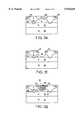
- FIGS. 3a to 3gFabrication of the structure of FIG. 2 is illustrated in FIGS. 3a to 3g.
- FIG. 3aone begins conventionally with an N+ doped substrate 40. Then one conventionally grows a first epitaxial layer 42 doped N type to a level of about 0.5 to 1.2 ohms ⁇ cm as shown in FIG. 3b. Then as shown in FIG. 3c a second epitaxial layer 46 is grown on the first epitaxial layer 42, the second epitaxial layer 46 being more lightly doped to a level of approximately 1.0 to 2.0 ohms ⁇ cm. All three regions 40, 42, 46 are doped using arsenic or phosphorous with arsenic preferred.
- the two epitaxial layers 42, 46have a thickness of approximately 3 to 8 microns ⁇ m, and 2 to 3 microns, respectively.
- the shallow P body in region 50is formed by boron implantation at 60 keV using a dose of 2 ⁇ 10 13 to 1 ⁇ 10 14 ion/cm 2 . This implantation is then driven into a depth of approximately 1.0 to 2.0 microns.
- the deep P body in region 50is then implanted in the central portion of the transistor using an implant dose of boron of 5 ⁇ 10 14 to 1 ⁇ 10 16 ion/cm 2 at an energy of 60 KeV. This implantation is then driven in to a depth of approximately 2.0 to 3.5 microns.
- the deep P body in region 50can be formed with a boron nitride process.
- the resulting sheet resistanceis about 20 to 100 ohm/square.
- the N+ region 52is conventionally implanted using a mask.
- the implantationis at an energy of 80 KeV and a dosage of 6 ⁇ 10 15 to 1 ⁇ 10 16 ion/cm 2 , again using arsenic or phosphorous.
- the N+ region 52is then driven in (diffused) to a depth of approximately 0.3 to 0.5 microns. (Also shown are N+ source regions 72, 80 of adjacent transistors which are formed simultaneously).
- a U-shaped trench 54is conventionally reactive ion etched through the central portion of the source region 52 into the body region 50 to a depth of approximately 1.0 to 2.0 microns.
- the trench 54is then conventionally lined (see FIG. 3g) with silicon dioxide 56 by thermal growth of silicon dioxide on the trench walls to a thickness of approximately 500 to 1000 ⁇ . Then the lined trench 54 is conventionally filled with polycrystalline silicon 60 which is then doped with phosphorous chloride to a sheet resistance of approximately 20 to 40 ohms/square. Then (not shown) an insulating (e.g. BPSG) layer is conventionally deposited and patterned for insulating the gate electrode. Then (not shown) the aluminum metallization layer is conventionally formed thereover, establishing electrical contact to the body and source regions.
- silicon dioxide 56by thermal growth of silicon dioxide on the trench walls to a thickness of approximately 500 to 1000 ⁇ .
- polycrystalline silicon 60which is then doped with phosphorous chloride to a sheet resistance of approximately 20 to 40 ohms/square.
- an insulating (e.g. BPSG) layeris conventionally deposited and patterned for insulating the gate electrode.
- the aluminum metallization layeris
- the final configuration of the device as shown in FIG. 2 with regard to channel lengthis a result of the double diffusion, i.e. diffusing the N+ source region 52 after establishing the P body region 50.
- the structure of FIG. 2may be formed by methods and materials other than as described above, so long as they result in two upper layers of the substrate, the upper most layer having a lower doping level than the layer immediately beneath it. This is most easily achieved through the above described double epitaxial layer growth, but other methods of establishing such a structure will be apparent to one of ordinary skill in the art.
- the P channel regionmay be formed after trench formation and planarization
- the upper epitaxial layer 46may be formed by implantation of boron into the epitaxial layer 42;
Landscapes
- Insulated Gate Type Field-Effect Transistor (AREA)
- Junction Field-Effect Transistors (AREA)
Abstract
Description
Claims (7)
Priority Applications (9)
| Application Number | Priority Date | Filing Date | Title |
|---|---|---|---|
| US07/918,954US5910669A (en) | 1992-07-24 | 1992-07-24 | Field effect Trench transistor having lightly doped epitaxial region on the surface portion thereof |
| KR1019930013750AKR100305978B1 (en) | 1992-07-24 | 1993-07-21 | Field-effect trench transistors with lightly doped epitaxial regions on the surface of transistors |
| DE0580452TDE580452T1 (en) | 1992-07-24 | 1993-07-23 | Field effect transistor with trench with a low doped epitaxial region on its surface area. |
| JP20259593AJP3387563B2 (en) | 1992-07-24 | 1993-07-23 | Field effect transistor and method of manufacturing the same |
| DE69309565TDE69309565T2 (en) | 1992-07-24 | 1993-07-23 | Field effect transistor with trench with a low doped epitaxial region on its surface area |
| EP93305856AEP0580452B1 (en) | 1992-07-24 | 1993-07-23 | Field effect trench transistor having lightly doped epitaxial region on the surface portion thereof |
| US08/386,895US5558313A (en) | 1992-07-24 | 1995-02-10 | Trench field effect transistor with reduced punch-through susceptibility and low RDSon |
| US08/447,484US5532179A (en) | 1992-07-24 | 1995-05-23 | Method of making a field effect trench transistor having lightly doped epitaxial region on the surface portion thereof |
| US08/658,115US5981344A (en) | 1992-07-24 | 1996-06-04 | Trench field effect transistor with reduced punch-through susceptibility and low RDSon |
Applications Claiming Priority (1)
| Application Number | Priority Date | Filing Date | Title |
|---|---|---|---|
| US07/918,954US5910669A (en) | 1992-07-24 | 1992-07-24 | Field effect Trench transistor having lightly doped epitaxial region on the surface portion thereof |
Related Child Applications (2)
| Application Number | Title | Priority Date | Filing Date |
|---|---|---|---|
| US08/386,895Continuation-In-PartUS5558313A (en) | 1992-07-24 | 1995-02-10 | Trench field effect transistor with reduced punch-through susceptibility and low RDSon |
| US08/447,484DivisionUS5532179A (en) | 1992-07-24 | 1995-05-23 | Method of making a field effect trench transistor having lightly doped epitaxial region on the surface portion thereof |
Publications (1)
| Publication Number | Publication Date |
|---|---|
| US5910669Atrue US5910669A (en) | 1999-06-08 |
Family
ID=25441223
Family Applications (2)
| Application Number | Title | Priority Date | Filing Date |
|---|---|---|---|
| US07/918,954Expired - LifetimeUS5910669A (en) | 1992-07-24 | 1992-07-24 | Field effect Trench transistor having lightly doped epitaxial region on the surface portion thereof |
| US08/447,484Expired - LifetimeUS5532179A (en) | 1992-07-24 | 1995-05-23 | Method of making a field effect trench transistor having lightly doped epitaxial region on the surface portion thereof |
Family Applications After (1)
| Application Number | Title | Priority Date | Filing Date |
|---|---|---|---|
| US08/447,484Expired - LifetimeUS5532179A (en) | 1992-07-24 | 1995-05-23 | Method of making a field effect trench transistor having lightly doped epitaxial region on the surface portion thereof |
Country Status (5)
| Country | Link |
|---|---|
| US (2) | US5910669A (en) |
| EP (1) | EP0580452B1 (en) |
| JP (1) | JP3387563B2 (en) |
| KR (1) | KR100305978B1 (en) |
| DE (2) | DE580452T1 (en) |
Cited By (31)
| Publication number | Priority date | Publication date | Assignee | Title |
|---|---|---|---|---|
| US6084264A (en)* | 1998-11-25 | 2000-07-04 | Siliconix Incorporated | Trench MOSFET having improved breakdown and on-resistance characteristics |
| US6163051A (en)* | 1995-08-24 | 2000-12-19 | Kabushiki Kaisha Toshiba | High breakdown voltage semiconductor device |
| US6188104B1 (en)* | 1997-03-27 | 2001-02-13 | Samsung Electronics Co., Ltd | Trench DMOS device having an amorphous silicon and polysilicon gate |
| US6395604B1 (en)* | 1997-08-08 | 2002-05-28 | Sanyo Electric Co., Ltd. | Method of fabricating semiconductor device |
| US6476442B1 (en)* | 1996-05-15 | 2002-11-05 | Siliconix Incorporated | Pseudo-Schottky diode |
| US6518624B2 (en)* | 2000-05-30 | 2003-02-11 | Fairchild Korea Semiconductor Ltd. | Trench-gate power semiconductor device preventing latch-up and method for fabricating the same |
| WO2003021639A3 (en)* | 2001-09-05 | 2003-07-31 | Int Rectifier Corp | Trench fet with self aligned source and contact |
| US20030198672A1 (en)* | 2001-08-14 | 2003-10-23 | Franz G. Andrew | Levothyroxine compositions having unique triidothyronine plasma AUC properties |
| US20030213993A1 (en)* | 2002-05-14 | 2003-11-20 | Kyle Spring | Trench mosfet with field relief feature |
| US20040038467A1 (en)* | 2001-07-03 | 2004-02-26 | Siliconix Incorporated | Trench MIS device having implanted drain-drift region and thick bottom oxide and process for manufacturing the same |
| US6710441B2 (en) | 2000-07-13 | 2004-03-23 | Isothermal Research Systems, Inc. | Power semiconductor switching devices, power converters, integrated circuit assemblies, integrated circuitry, power current switching methods, methods of forming a power semiconductor switching device, power conversion methods, power semiconductor switching device packaging methods, and methods of forming a power transistor |
| US20040195620A1 (en)* | 2003-03-28 | 2004-10-07 | Mosel Vitelic, Inc. | Termination structure of DMOS device |
| US20050006700A1 (en)* | 2003-06-11 | 2005-01-13 | International Rectifier Corporation | Low on resistance power MOSFET with variably spaced trenches and offset contacts |
| US20050017294A1 (en)* | 2001-04-02 | 2005-01-27 | Shindengen Electric Manufacturing Co., Ltd. | Semiconductor device having shallow trenches and method for manufacturing the same |
| US20050173757A1 (en)* | 2002-04-18 | 2005-08-11 | Peake Steven T. | Trench-gate semiconductor devices |
| US20050236665A1 (en)* | 2001-07-03 | 2005-10-27 | Darwish Mohamed N | Trench MIS device having implanted drain-drift region and thick bottom oxide and process for manufacturing the same |
| US20060038223A1 (en)* | 2001-07-03 | 2006-02-23 | Siliconix Incorporated | Trench MOSFET having drain-drift region comprising stack of implanted regions |
| US20060121676A1 (en)* | 2001-07-03 | 2006-06-08 | Siliconix Incorporated | Trench MIS device with thick oxide layer in bottom of gate contact trench |
| US20080265318A1 (en)* | 2003-09-10 | 2008-10-30 | Infineon Technologies Ag | Semiconductor component and method for producing it |
| US20090050958A1 (en)* | 2004-05-21 | 2009-02-26 | Qi Wang | Semiconductor device having a spacer layer doped with slower diffusing atoms than substrate |
| US8053329B2 (en) | 2000-02-16 | 2011-11-08 | Ziptronix, Inc. | Method for low temperature bonding and bonded structure |
| US8283721B2 (en) | 2008-03-26 | 2012-10-09 | Rohm Co., Ltd. | Semiconductor device, and method for manufacturing the same |
| US20140291756A1 (en)* | 2013-03-26 | 2014-10-02 | Toyoda Gosei Co., Ltd. | Semiconductor device and manufacturing method thereof |
| US20180040687A1 (en)* | 2016-08-05 | 2018-02-08 | Fuji Electric Co., Ltd. | Semiconductor device and method of manufacturing semiconductor device |
| US10026835B2 (en) | 2009-10-28 | 2018-07-17 | Vishay-Siliconix | Field boosted metal-oxide-semiconductor field effect transistor |
| US10153356B2 (en) | 2016-03-24 | 2018-12-11 | Toyoda Gosei Co., Ltd. | Method of manufacturing semiconductor device, and semiconductor device |
| US10256323B2 (en) | 2016-03-24 | 2019-04-09 | Toyoda Gosei Co., Ltd. | Method of manufacturing semiconductor device including an n type semiconductor region formed in a p type semiconductor layer |
| US10490408B2 (en) | 2017-03-28 | 2019-11-26 | Toyoda Gosei Co., Ltd. | Method for manufacturing semiconductor device |
| US10879349B2 (en) | 2017-03-28 | 2020-12-29 | Toyoda Goset Co., Ltd. | Method for manufacturing semiconductor device and edge termination structure of semiconductor device |
| US10923587B2 (en) | 2015-10-28 | 2021-02-16 | Robert Bosch Gmbh | Power MOSFET and method for producing a power MOSFET |
| CN116469923A (en)* | 2023-04-25 | 2023-07-21 | 南京第三代半导体技术创新中心有限公司 | High-reliability trench silicon carbide MOSFET device and manufacturing method thereof |
Families Citing this family (62)
| Publication number | Priority date | Publication date | Assignee | Title |
|---|---|---|---|---|
| US6603173B1 (en) | 1991-07-26 | 2003-08-05 | Denso Corporation | Vertical type MOSFET |
| US6015737A (en)* | 1991-07-26 | 2000-01-18 | Denso Corporation | Production method of a vertical type MOSFET |
| US5558313A (en)* | 1992-07-24 | 1996-09-24 | Siliconix Inorporated | Trench field effect transistor with reduced punch-through susceptibility and low RDSon |
| EP0675529A3 (en)* | 1994-03-30 | 1998-06-03 | Denso Corporation | Process for manufacturing vertical MOS transistors |
| US5780324A (en)* | 1994-03-30 | 1998-07-14 | Denso Corporation | Method of manufacturing a vertical semiconductor device |
| US5674766A (en)* | 1994-12-30 | 1997-10-07 | Siliconix Incorporated | Method of making a trench MOSFET with multi-resistivity drain to provide low on-resistance by varying dopant concentration in epitaxial layer |
| US5688725A (en)* | 1994-12-30 | 1997-11-18 | Siliconix Incorporated | Method of making a trench mosfet with heavily doped delta layer to provide low on-resistance |
| EP0735591B1 (en)* | 1995-03-31 | 1999-09-08 | Consorzio per la Ricerca sulla Microelettronica nel Mezzogiorno | Improved DMOS device structure, and related manufacturing process |
| US5567634A (en)* | 1995-05-01 | 1996-10-22 | National Semiconductor Corporation | Method of fabricating self-aligned contact trench DMOS transistors |
| US6049108A (en)* | 1995-06-02 | 2000-04-11 | Siliconix Incorporated | Trench-gated MOSFET with bidirectional voltage clamping |
| WO1997007548A1 (en)* | 1995-08-21 | 1997-02-27 | Siliconix Incorporated | Low voltage short channel trench dmos transistor |
| US5629543A (en)* | 1995-08-21 | 1997-05-13 | Siliconix Incorporated | Trenched DMOS transistor with buried layer for reduced on-resistance and ruggedness |
| US5821583A (en)* | 1996-03-06 | 1998-10-13 | Siliconix Incorporated | Trenched DMOS transistor with lightly doped tub |
| US5814858A (en)* | 1996-03-15 | 1998-09-29 | Siliconix Incorporated | Vertical power MOSFET having reduced sensitivity to variations in thickness of epitaxial layer |
| JP3217690B2 (en)* | 1996-03-22 | 2001-10-09 | 株式会社東芝 | Method for manufacturing semiconductor device |
| US5719409A (en)* | 1996-06-06 | 1998-02-17 | Cree Research, Inc. | Silicon carbide metal-insulator semiconductor field effect transistor |
| US6096608A (en)* | 1997-06-30 | 2000-08-01 | Siliconix Incorporated | Bidirectional trench gated power mosfet with submerged body bus extending underneath gate trench |
| US6103635A (en)* | 1997-10-28 | 2000-08-15 | Fairchild Semiconductor Corp. | Trench forming process and integrated circuit device including a trench |
| JP2011035410A (en)* | 1997-10-31 | 2011-02-17 | Siliconix Inc | Trench-gate power mosfet equipped with protecting diode |
| US6429481B1 (en)* | 1997-11-14 | 2002-08-06 | Fairchild Semiconductor Corporation | Field effect transistor and method of its manufacture |
| GB9808234D0 (en)* | 1998-04-17 | 1998-06-17 | Koninkl Philips Electronics Nv | Mnufacture of trench-gate semiconductor devices |
| US5937297A (en)* | 1998-06-01 | 1999-08-10 | Chartered Semiconductor Manufacturing, Ltd. | Method for making sub-quarter-micron MOSFET |
| US6614074B2 (en) | 1998-06-05 | 2003-09-02 | International Business Machines Corporation | Grooved planar DRAM transfer device using buried pocket |
| US5998833A (en)* | 1998-10-26 | 1999-12-07 | North Carolina State University | Power semiconductor devices having improved high frequency switching and breakdown characteristics |
| US6621121B2 (en) | 1998-10-26 | 2003-09-16 | Silicon Semiconductor Corporation | Vertical MOSFETs having trench-based gate electrodes within deeper trench-based source electrodes |
| US6191447B1 (en) | 1999-05-28 | 2001-02-20 | Micro-Ohm Corporation | Power semiconductor devices that utilize tapered trench-based insulating regions to improve electric field profiles in highly doped drift region mesas and methods of forming same |
| TW411553B (en)* | 1999-08-04 | 2000-11-11 | Mosel Vitelic Inc | Method for forming curved oxide on bottom of trench |
| JP4738562B2 (en)* | 2000-03-15 | 2011-08-03 | 三菱電機株式会社 | Manufacturing method of semiconductor device |
| US6472678B1 (en)* | 2000-06-16 | 2002-10-29 | General Semiconductor, Inc. | Trench MOSFET with double-diffused body profile |
| US6593620B1 (en) | 2000-10-06 | 2003-07-15 | General Semiconductor, Inc. | Trench DMOS transistor with embedded trench schottky rectifier |
| US7345342B2 (en) | 2001-01-30 | 2008-03-18 | Fairchild Semiconductor Corporation | Power semiconductor devices and methods of manufacture |
| US6916745B2 (en) | 2003-05-20 | 2005-07-12 | Fairchild Semiconductor Corporation | Structure and method for forming a trench MOSFET having self-aligned features |
| US7132712B2 (en) | 2002-11-05 | 2006-11-07 | Fairchild Semiconductor Corporation | Trench structure having one or more diodes embedded therein adjacent a PN junction |
| US7061066B2 (en) | 2001-10-17 | 2006-06-13 | Fairchild Semiconductor Corporation | Schottky diode using charge balance structure |
| US7078296B2 (en) | 2002-01-16 | 2006-07-18 | Fairchild Semiconductor Corporation | Self-aligned trench MOSFETs and methods for making the same |
| KR100859701B1 (en) | 2002-02-23 | 2008-09-23 | 페어차일드코리아반도체 주식회사 | High voltage horizontal MOS transistor and method for manufacturing same |
| US7576388B1 (en) | 2002-10-03 | 2009-08-18 | Fairchild Semiconductor Corporation | Trench-gate LDMOS structures |
| US7282302B2 (en)* | 2002-10-15 | 2007-10-16 | Polyplus Battery Company | Ionically conductive composites for protection of active metal anodes |
| TWI230456B (en)* | 2003-05-14 | 2005-04-01 | Promos Technologies Inc | Shallow trench isolation and dynamic random access memory and fabricating methods thereof |
| US7652326B2 (en) | 2003-05-20 | 2010-01-26 | Fairchild Semiconductor Corporation | Power semiconductor devices and methods of manufacture |
| JP3954541B2 (en)* | 2003-08-05 | 2007-08-08 | 株式会社東芝 | Semiconductor device and manufacturing method thereof |
| TWI222685B (en)* | 2003-12-18 | 2004-10-21 | Episil Technologies Inc | Metal oxide semiconductor device and fabricating method thereof |
| US7368777B2 (en) | 2003-12-30 | 2008-05-06 | Fairchild Semiconductor Corporation | Accumulation device with charge balance structure and method of forming the same |
| US7352036B2 (en) | 2004-08-03 | 2008-04-01 | Fairchild Semiconductor Corporation | Semiconductor power device having a top-side drain using a sinker trench |
| CN101185169B (en) | 2005-04-06 | 2010-08-18 | 飞兆半导体公司 | Trench gate field effect transistor and method of forming the same |
| JP5008046B2 (en) | 2005-06-14 | 2012-08-22 | ローム株式会社 | Semiconductor device |
| US7385248B2 (en) | 2005-08-09 | 2008-06-10 | Fairchild Semiconductor Corporation | Shielded gate field effect transistor with improved inter-poly dielectric |
| US7446374B2 (en)* | 2006-03-24 | 2008-11-04 | Fairchild Semiconductor Corporation | High density trench FET with integrated Schottky diode and method of manufacture |
| US7319256B1 (en) | 2006-06-19 | 2008-01-15 | Fairchild Semiconductor Corporation | Shielded gate trench FET with the shield and gate electrodes being connected together |
| US8896093B2 (en)* | 2012-12-19 | 2014-11-25 | Alpha And Omega Semiconductor Incorporated | Circuit configuration and manufacturing processes for vertical transient voltage suppressor (TVS) and EMI filter |
| JP2008218711A (en)* | 2007-03-05 | 2008-09-18 | Renesas Technology Corp | Semiconductor device, manufacturing method thereof, and power supply device |
| JP5767430B2 (en)* | 2007-08-10 | 2015-08-19 | ローム株式会社 | Semiconductor device and manufacturing method of semiconductor device |
| US7772668B2 (en) | 2007-12-26 | 2010-08-10 | Fairchild Semiconductor Corporation | Shielded gate trench FET with multiple channels |
| US8174067B2 (en) | 2008-12-08 | 2012-05-08 | Fairchild Semiconductor Corporation | Trench-based power semiconductor devices with increased breakdown voltage characteristics |
| US8067304B2 (en)* | 2009-01-20 | 2011-11-29 | Alpha And Omega Semiconductor, Inc. | Method for forming a patterned thick metallization atop a power semiconductor chip |
| US9653597B2 (en) | 2010-05-20 | 2017-05-16 | Infineon Technologies Americas Corp. | Method for fabricating a shallow and narrow trench FET and related structures |
| US8432000B2 (en) | 2010-06-18 | 2013-04-30 | Fairchild Semiconductor Corporation | Trench MOS barrier schottky rectifier with a planar surface using CMP techniques |
| CN103035645B (en)* | 2012-08-10 | 2015-08-19 | 上海华虹宏力半导体制造有限公司 | A kind of trench gate metal-oxide-semiconductor and manufacture method thereof |
| WO2014207793A1 (en)* | 2013-06-24 | 2014-12-31 | 株式会社日立製作所 | Semiconductor device, and method for manufacturing same |
| JP6613610B2 (en) | 2015-05-14 | 2019-12-04 | 富士電機株式会社 | Semiconductor device and manufacturing method of semiconductor device |
| CN109273529A (en)* | 2017-07-18 | 2019-01-25 | 比亚迪股份有限公司 | MOS type power device and preparation method thereof |
| US10438813B2 (en) | 2017-11-13 | 2019-10-08 | Alpha And Omega Semiconductor (Cayman) Ltd. | Semiconductor device having one or more titanium interlayers and method of making the same |
Citations (13)
| Publication number | Priority date | Publication date | Assignee | Title |
|---|---|---|---|---|
| JPS55146976A (en)* | 1979-05-02 | 1980-11-15 | Nec Corp | Insulating gate field effect transistor |
| JPS5658267A (en)* | 1979-10-17 | 1981-05-21 | Nippon Telegr & Teleph Corp <Ntt> | Insulated gate type field-effect transistor |
| JPS5984474A (en)* | 1982-11-05 | 1984-05-16 | Nec Corp | Vertical field effect transistor for power use |
| US4593302A (en)* | 1980-08-18 | 1986-06-03 | International Rectifier Corporation | Process for manufacture of high power MOSFET with laterally distributed high carrier density beneath the gate oxide |
| US4680853A (en)* | 1980-08-18 | 1987-07-21 | International Rectifier Corporation | Process for manufacture of high power MOSFET with laterally distributed high carrier density beneath the gate oxide |
| JPS62176168A (en)* | 1986-01-30 | 1987-08-01 | Nippon Denso Co Ltd | Vertical MOS transistor |
| US4803532A (en)* | 1982-11-27 | 1989-02-07 | Nissan Motor Co., Ltd. | Vertical MOSFET having a proof structure against puncture due to breakdown |
| JPS6442177A (en)* | 1987-08-10 | 1989-02-14 | Hitachi Ltd | Insulated gate transistor |
| EP0345380A2 (en)* | 1988-06-08 | 1989-12-13 | Mitsubishi Denki Kabushiki Kaisha | Manufacture of a semiconductor device |
| US4941026A (en)* | 1986-12-05 | 1990-07-10 | General Electric Company | Semiconductor devices exhibiting minimum on-resistance |
| US5072266A (en)* | 1988-12-27 | 1991-12-10 | Siliconix Incorporated | Trench DMOS power transistor with field-shaping body profile and three-dimensional geometry |
| US5138422A (en)* | 1987-10-27 | 1992-08-11 | Nippondenso Co., Ltd. | Semiconductor device which includes multiple isolated semiconductor segments on one chip |
| US5168331A (en)* | 1991-01-31 | 1992-12-01 | Siliconix Incorporated | Power metal-oxide-semiconductor field effect transistor |
Family Cites Families (7)
| Publication number | Priority date | Publication date | Assignee | Title |
|---|---|---|---|---|
| US5017504A (en)* | 1986-12-01 | 1991-05-21 | Mitsubishi Denki Kabushiki Kaisha | Vertical type MOS transistor and method of formation thereof |
| US4893160A (en)* | 1987-11-13 | 1990-01-09 | Siliconix Incorporated | Method for increasing the performance of trenched devices and the resulting structure |
| GB9215653D0 (en)* | 1992-07-23 | 1992-09-09 | Philips Electronics Uk Ltd | A method of manufacturing a semiconductor device comprising an insulated gate field effect device |
| JPH06104445A (en)* | 1992-08-04 | 1994-04-15 | Siliconix Inc | Power MOS transistor and method of manufacturing the same |
| US5341011A (en)* | 1993-03-15 | 1994-08-23 | Siliconix Incorporated | Short channel trenched DMOS transistor |
| JPH07122749A (en)* | 1993-09-01 | 1995-05-12 | Toshiba Corp | Semiconductor device and manufacturing method thereof |
| US5405794A (en)* | 1994-06-14 | 1995-04-11 | Philips Electronics North America Corporation | Method of producing VDMOS device of increased power density |
- 1992
- 1992-07-24USUS07/918,954patent/US5910669A/ennot_activeExpired - Lifetime
- 1993
- 1993-07-21KRKR1019930013750Apatent/KR100305978B1/ennot_activeExpired - Lifetime
- 1993-07-23DEDE0580452Tpatent/DE580452T1/enactivePending
- 1993-07-23DEDE69309565Tpatent/DE69309565T2/ennot_activeExpired - Fee Related
- 1993-07-23EPEP93305856Apatent/EP0580452B1/ennot_activeExpired - Lifetime
- 1993-07-23JPJP20259593Apatent/JP3387563B2/ennot_activeExpired - Lifetime
- 1995
- 1995-05-23USUS08/447,484patent/US5532179A/ennot_activeExpired - Lifetime
Patent Citations (14)
| Publication number | Priority date | Publication date | Assignee | Title |
|---|---|---|---|---|
| JPS55146976A (en)* | 1979-05-02 | 1980-11-15 | Nec Corp | Insulating gate field effect transistor |
| JPS5658267A (en)* | 1979-10-17 | 1981-05-21 | Nippon Telegr & Teleph Corp <Ntt> | Insulated gate type field-effect transistor |
| US4593302A (en)* | 1980-08-18 | 1986-06-03 | International Rectifier Corporation | Process for manufacture of high power MOSFET with laterally distributed high carrier density beneath the gate oxide |
| US4680853A (en)* | 1980-08-18 | 1987-07-21 | International Rectifier Corporation | Process for manufacture of high power MOSFET with laterally distributed high carrier density beneath the gate oxide |
| US4593302B1 (en)* | 1980-08-18 | 1998-02-03 | Int Rectifier Corp | Process for manufacture of high power mosfet laterally distributed high carrier density beneath the gate oxide |
| JPS5984474A (en)* | 1982-11-05 | 1984-05-16 | Nec Corp | Vertical field effect transistor for power use |
| US4803532A (en)* | 1982-11-27 | 1989-02-07 | Nissan Motor Co., Ltd. | Vertical MOSFET having a proof structure against puncture due to breakdown |
| JPS62176168A (en)* | 1986-01-30 | 1987-08-01 | Nippon Denso Co Ltd | Vertical MOS transistor |
| US4941026A (en)* | 1986-12-05 | 1990-07-10 | General Electric Company | Semiconductor devices exhibiting minimum on-resistance |
| JPS6442177A (en)* | 1987-08-10 | 1989-02-14 | Hitachi Ltd | Insulated gate transistor |
| US5138422A (en)* | 1987-10-27 | 1992-08-11 | Nippondenso Co., Ltd. | Semiconductor device which includes multiple isolated semiconductor segments on one chip |
| EP0345380A2 (en)* | 1988-06-08 | 1989-12-13 | Mitsubishi Denki Kabushiki Kaisha | Manufacture of a semiconductor device |
| US5072266A (en)* | 1988-12-27 | 1991-12-10 | Siliconix Incorporated | Trench DMOS power transistor with field-shaping body profile and three-dimensional geometry |
| US5168331A (en)* | 1991-01-31 | 1992-12-01 | Siliconix Incorporated | Power metal-oxide-semiconductor field effect transistor |
Cited By (62)
| Publication number | Priority date | Publication date | Assignee | Title |
|---|---|---|---|---|
| US6163051A (en)* | 1995-08-24 | 2000-12-19 | Kabushiki Kaisha Toshiba | High breakdown voltage semiconductor device |
| US6476442B1 (en)* | 1996-05-15 | 2002-11-05 | Siliconix Incorporated | Pseudo-Schottky diode |
| US6188104B1 (en)* | 1997-03-27 | 2001-02-13 | Samsung Electronics Co., Ltd | Trench DMOS device having an amorphous silicon and polysilicon gate |
| US6395604B1 (en)* | 1997-08-08 | 2002-05-28 | Sanyo Electric Co., Ltd. | Method of fabricating semiconductor device |
| US6084264A (en)* | 1998-11-25 | 2000-07-04 | Siliconix Incorporated | Trench MOSFET having improved breakdown and on-resistance characteristics |
| US8053329B2 (en) | 2000-02-16 | 2011-11-08 | Ziptronix, Inc. | Method for low temperature bonding and bonded structure |
| US6518624B2 (en)* | 2000-05-30 | 2003-02-11 | Fairchild Korea Semiconductor Ltd. | Trench-gate power semiconductor device preventing latch-up and method for fabricating the same |
| US6710441B2 (en) | 2000-07-13 | 2004-03-23 | Isothermal Research Systems, Inc. | Power semiconductor switching devices, power converters, integrated circuit assemblies, integrated circuitry, power current switching methods, methods of forming a power semiconductor switching device, power conversion methods, power semiconductor switching device packaging methods, and methods of forming a power transistor |
| US20050230746A1 (en)* | 2000-07-13 | 2005-10-20 | Eden Richard C | Power semiconductor switching devices and power semiconductor devices |
| US7019337B2 (en) | 2000-07-13 | 2006-03-28 | Isothermal Systems Research, Inc. | Power semiconductor switching devices, power converters, integrated circuit assemblies, integrated circuitry, power current switching methods, methods of forming a power semiconductor switching device, power conversion methods, power semiconductor switching device packaging methods, and methods of forming a power transistor |
| US6737301B2 (en) | 2000-07-13 | 2004-05-18 | Isothermal Systems Research, Inc. | Power semiconductor switching devices, power converters, integrated circuit assemblies, integrated circuitry, power current switching methods, methods of forming a power semiconductor switching device, power conversion methods, power semiconductor switching device packaging methods, and methods of forming a power transistor |
| US20050017294A1 (en)* | 2001-04-02 | 2005-01-27 | Shindengen Electric Manufacturing Co., Ltd. | Semiconductor device having shallow trenches and method for manufacturing the same |
| US7397082B2 (en)* | 2001-04-02 | 2008-07-08 | Shindengen Electric Manufacturing Co., Ltd. | Semiconductor device having shallow trenches and method for manufacturing the same |
| US20060121676A1 (en)* | 2001-07-03 | 2006-06-08 | Siliconix Incorporated | Trench MIS device with thick oxide layer in bottom of gate contact trench |
| US7435650B2 (en) | 2001-07-03 | 2008-10-14 | Siliconix Incorporated | Process for manufacturing trench MIS device having implanted drain-drift region and thick bottom oxide |
| US20040227182A1 (en)* | 2001-07-03 | 2004-11-18 | Siliconix Incorporated | Process for manufacturing trench MIS device having implanted drain-drift region and thick botton oxide |
| US7416947B2 (en) | 2001-07-03 | 2008-08-26 | Siliconix Incorporated | Method of fabricating trench MIS device with thick oxide layer in bottom of trench |
| US7291884B2 (en)* | 2001-07-03 | 2007-11-06 | Siliconix Incorporated | Trench MIS device having implanted drain-drift region and thick bottom oxide |
| US7326995B2 (en) | 2001-07-03 | 2008-02-05 | Siliconix Incorporated | Trench MIS device having implanted drain-drift region and thick bottom oxide |
| US20050236665A1 (en)* | 2001-07-03 | 2005-10-27 | Darwish Mohamed N | Trench MIS device having implanted drain-drift region and thick bottom oxide and process for manufacturing the same |
| US20060038223A1 (en)* | 2001-07-03 | 2006-02-23 | Siliconix Incorporated | Trench MOSFET having drain-drift region comprising stack of implanted regions |
| US20040038467A1 (en)* | 2001-07-03 | 2004-02-26 | Siliconix Incorporated | Trench MIS device having implanted drain-drift region and thick bottom oxide and process for manufacturing the same |
| US20030198672A1 (en)* | 2001-08-14 | 2003-10-23 | Franz G. Andrew | Levothyroxine compositions having unique triidothyronine plasma AUC properties |
| US7045859B2 (en) | 2001-09-05 | 2006-05-16 | International Rectifier Corporation | Trench fet with self aligned source and contact |
| US20060157782A1 (en)* | 2001-09-05 | 2006-07-20 | International Rectifier Corporation | Trench fet with self aligned source and contact |
| US7397083B2 (en) | 2001-09-05 | 2008-07-08 | International Rectifier Corporation | Trench fet with self aligned source and contact |
| US20080061365A1 (en)* | 2001-09-05 | 2008-03-13 | International Rectifier Corporation | Trench fet with self aligned source and contact |
| WO2003021639A3 (en)* | 2001-09-05 | 2003-07-31 | Int Rectifier Corp | Trench fet with self aligned source and contact |
| US7301200B2 (en)* | 2001-09-05 | 2007-11-27 | International Rectifier Corporation | Trench FET with self aligned source and contact |
| US20050173757A1 (en)* | 2002-04-18 | 2005-08-11 | Peake Steven T. | Trench-gate semiconductor devices |
| US7332771B2 (en)* | 2002-04-18 | 2008-02-19 | Nxp, B.V. | Trench-gate semiconductor devices |
| US7161208B2 (en) | 2002-05-14 | 2007-01-09 | International Rectifier Corporation | Trench mosfet with field relief feature |
| US20030213993A1 (en)* | 2002-05-14 | 2003-11-20 | Kyle Spring | Trench mosfet with field relief feature |
| US7087958B2 (en)* | 2003-03-28 | 2006-08-08 | Mosel Vitelic, Inc. | Termination structure of DMOS device |
| US20040195620A1 (en)* | 2003-03-28 | 2004-10-07 | Mosel Vitelic, Inc. | Termination structure of DMOS device |
| US7075147B2 (en)* | 2003-06-11 | 2006-07-11 | International Rectifier Corporation | Low on resistance power MOSFET with variably spaced trenches and offset contacts |
| US20050006700A1 (en)* | 2003-06-11 | 2005-01-13 | International Rectifier Corporation | Low on resistance power MOSFET with variably spaced trenches and offset contacts |
| US20080265318A1 (en)* | 2003-09-10 | 2008-10-30 | Infineon Technologies Ag | Semiconductor component and method for producing it |
| US7863680B2 (en)* | 2003-09-10 | 2011-01-04 | Infineon Technologies Ag | Semiconductor component and method for producing it |
| US20090050958A1 (en)* | 2004-05-21 | 2009-02-26 | Qi Wang | Semiconductor device having a spacer layer doped with slower diffusing atoms than substrate |
| US8283721B2 (en) | 2008-03-26 | 2012-10-09 | Rohm Co., Ltd. | Semiconductor device, and method for manufacturing the same |
| CN101981701B (en)* | 2008-03-26 | 2013-10-02 | 罗姆股份有限公司 | Semiconductor device and manufacturing method thereof |
| US11127851B2 (en) | 2008-03-26 | 2021-09-21 | Rohm Co., Ltd. | Semiconductor device, and method for manufacturing the same |
| US9166038B2 (en) | 2008-03-26 | 2015-10-20 | Rohm Co., Ltd. | Semiconductor device, and method for manufacturing the same |
| US12009420B2 (en) | 2008-03-26 | 2024-06-11 | Rohm Co., Ltd. | Semiconductor device, and method for manufacturing the same |
| US9496387B2 (en) | 2008-03-26 | 2016-11-15 | Rohm Co., Ltd. | Semiconductor device, and method for manufacturing the same |
| US10290733B2 (en) | 2008-03-26 | 2019-05-14 | Rohm Co., Ltd. | Semiconductor device, and method for manufacturing the same |
| US10686067B2 (en) | 2008-03-26 | 2020-06-16 | Rohm Co., Ltd. | Semiconductor device, and method for manufacturing the same |
| US12034073B2 (en) | 2008-03-26 | 2024-07-09 | Rohm Co., Ltd. | Semiconductor device, and method for manufacturing the same |
| US10026835B2 (en) | 2009-10-28 | 2018-07-17 | Vishay-Siliconix | Field boosted metal-oxide-semiconductor field effect transistor |
| US20140291756A1 (en)* | 2013-03-26 | 2014-10-02 | Toyoda Gosei Co., Ltd. | Semiconductor device and manufacturing method thereof |
| US9349856B2 (en)* | 2013-03-26 | 2016-05-24 | Toyoda Gosei Co., Ltd. | Semiconductor device including first interface and second interface as an upper surface of a convex protruded from first interface and manufacturing device thereof |
| TWI730994B (en)* | 2015-10-28 | 2021-06-21 | 德商羅伯特博斯奇股份有限公司 | Power mosfet and process to fabricate a power mosfet |
| US10923587B2 (en) | 2015-10-28 | 2021-02-16 | Robert Bosch Gmbh | Power MOSFET and method for producing a power MOSFET |
| US10256323B2 (en) | 2016-03-24 | 2019-04-09 | Toyoda Gosei Co., Ltd. | Method of manufacturing semiconductor device including an n type semiconductor region formed in a p type semiconductor layer |
| US10153356B2 (en) | 2016-03-24 | 2018-12-11 | Toyoda Gosei Co., Ltd. | Method of manufacturing semiconductor device, and semiconductor device |
| US20180040687A1 (en)* | 2016-08-05 | 2018-02-08 | Fuji Electric Co., Ltd. | Semiconductor device and method of manufacturing semiconductor device |
| US10886365B2 (en)* | 2016-08-05 | 2021-01-05 | Fuji Electric Co., Ltd. | Semiconductor device and method of manufacturing semiconductor device |
| US10879349B2 (en) | 2017-03-28 | 2020-12-29 | Toyoda Goset Co., Ltd. | Method for manufacturing semiconductor device and edge termination structure of semiconductor device |
| US10490408B2 (en) | 2017-03-28 | 2019-11-26 | Toyoda Gosei Co., Ltd. | Method for manufacturing semiconductor device |
| CN116469923A (en)* | 2023-04-25 | 2023-07-21 | 南京第三代半导体技术创新中心有限公司 | High-reliability trench silicon carbide MOSFET device and manufacturing method thereof |
| CN116469923B (en)* | 2023-04-25 | 2023-10-20 | 南京第三代半导体技术创新中心有限公司 | High-reliability trench silicon carbide MOSFET device and manufacturing method thereof |
Also Published As
| Publication number | Publication date |
|---|---|
| DE580452T1 (en) | 1994-10-06 |
| DE69309565D1 (en) | 1997-05-15 |
| US5532179A (en) | 1996-07-02 |
| JP3387563B2 (en) | 2003-03-17 |
| EP0580452B1 (en) | 1997-04-09 |
| JPH06224437A (en) | 1994-08-12 |
| KR940003092A (en) | 1994-02-19 |
| KR100305978B1 (en) | 2001-12-15 |
| DE69309565T2 (en) | 1997-07-24 |
| EP0580452A1 (en) | 1994-01-26 |
Similar Documents
| Publication | Publication Date | Title |
|---|---|---|
| US5910669A (en) | Field effect Trench transistor having lightly doped epitaxial region on the surface portion thereof | |
| US5929481A (en) | High density trench DMOS transistor with trench bottom implant | |
| US6069043A (en) | Method of making punch-through field effect transistor | |
| US7323386B2 (en) | Method of fabricating semiconductor device containing dielectrically isolated PN junction for enhanced breakdown characteristics | |
| US5689128A (en) | High density trenched DMOS transistor | |
| US5474943A (en) | Method for fabricating a short channel trenched DMOS transistor | |
| US6992350B2 (en) | High voltage power MOSFET having low on-resistance | |
| US5597765A (en) | Method for making termination structure for power MOSFET | |
| US7094640B2 (en) | Method of making a trench MOSFET device with improved on-resistance | |
| KR100958421B1 (en) | Power device and manufacturing method thereof | |
| US7015125B2 (en) | Trench MOSFET device with polycrystalline silicon source contact structure | |
| US5382536A (en) | Method of fabricating lateral DMOS structure | |
| KR20040030836A (en) | Manufacture of semiconductor devices with schottky barriers | |
| KR20000071468A (en) | Improved Power Trench MOS-Gated Device And Process For Forming Same | |
| US20030222290A1 (en) | Power device having reduced reverse bias leakage current | |
| US20220130997A1 (en) | Gate trench power semiconductor devices having improved deep shield connection patterns | |
| US9905675B1 (en) | Gate and field electrode trench formation process |
Legal Events
| Date | Code | Title | Description |
|---|---|---|---|
| AS | Assignment | Owner name:SILICONIX, INCORPORATED A CORP. OF CALIFORNIA, Free format text:ASSIGNMENT OF ASSIGNORS INTEREST.;ASSIGNORS:CHANG, MIKE F.;HSHIEH, FWU-IUAN;KWAN, SZE-HON;AND OTHERS;REEL/FRAME:006228/0359 Effective date:19920714 | |
| STCF | Information on status: patent grant | Free format text:PATENTED CASE | |
| FPAY | Fee payment | Year of fee payment:4 | |
| FPAY | Fee payment | Year of fee payment:8 | |
| AS | Assignment | Owner name:COMERICA BANK, AS AGENT,MICHIGAN Free format text:SECURITY AGREEMENT;ASSIGNORS:VISHAY SPRAGUE, INC., SUCCESSOR IN INTEREST TO VISHAY EFI, INC. AND VISHAY THIN FILM, LLC;VISHAY DALE ELECTRONICS, INC.;VISHAY INTERTECHNOLOGY, INC.;AND OTHERS;REEL/FRAME:024006/0515 Effective date:20100212 Owner name:COMERICA BANK, AS AGENT, MICHIGAN Free format text:SECURITY AGREEMENT;ASSIGNORS:VISHAY SPRAGUE, INC., SUCCESSOR IN INTEREST TO VISHAY EFI, INC. AND VISHAY THIN FILM, LLC;VISHAY DALE ELECTRONICS, INC.;VISHAY INTERTECHNOLOGY, INC.;AND OTHERS;REEL/FRAME:024006/0515 Effective date:20100212 | |
| FPAY | Fee payment | Year of fee payment:12 | |
| AS | Assignment | Owner name:VISHAY DALE ELECTRONICS, INC., A DELAWARE CORPORAT Free format text:RELEASE BY SECURED PARTY;ASSIGNOR:COMERICA BANK, AS AGENT, A TEXAS BANKING ASSOCIATION (FORMERLY A MICHIGAN BANKING CORPORATION);REEL/FRAME:025489/0184 Effective date:20101201 Owner name:VISHAY GENERAL SEMICONDUCTOR, LLC, F/K/A GENERAL S Free format text:RELEASE BY SECURED PARTY;ASSIGNOR:COMERICA BANK, AS AGENT, A TEXAS BANKING ASSOCIATION (FORMERLY A MICHIGAN BANKING CORPORATION);REEL/FRAME:025489/0184 Effective date:20101201 Owner name:VISHAY VITRAMON, INCORPORATED, A DELAWARE CORPORAT Free format text:RELEASE BY SECURED PARTY;ASSIGNOR:COMERICA BANK, AS AGENT, A TEXAS BANKING ASSOCIATION (FORMERLY A MICHIGAN BANKING CORPORATION);REEL/FRAME:025489/0184 Effective date:20101201 Owner name:YOSEMITE INVESTMENT, INC., AN INDIANA CORPORATION, Free format text:RELEASE BY SECURED PARTY;ASSIGNOR:COMERICA BANK, AS AGENT, A TEXAS BANKING ASSOCIATION (FORMERLY A MICHIGAN BANKING CORPORATION);REEL/FRAME:025489/0184 Effective date:20101201 Owner name:VISHAY MEASUREMENTS GROUP, INC., A DELAWARE CORPOR Free format text:RELEASE BY SECURED PARTY;ASSIGNOR:COMERICA BANK, AS AGENT, A TEXAS BANKING ASSOCIATION (FORMERLY A MICHIGAN BANKING CORPORATION);REEL/FRAME:025489/0184 Effective date:20101201 Owner name:VISHAY INTERTECHNOLOGY, INC., A DELAWARE CORPORATI Free format text:RELEASE BY SECURED PARTY;ASSIGNOR:COMERICA BANK, AS AGENT, A TEXAS BANKING ASSOCIATION (FORMERLY A MICHIGAN BANKING CORPORATION);REEL/FRAME:025489/0184 Effective date:20101201 Owner name:SILICONIX INCORPORATED, A DELAWARE CORPORATION, PE Free format text:RELEASE BY SECURED PARTY;ASSIGNOR:COMERICA BANK, AS AGENT, A TEXAS BANKING ASSOCIATION (FORMERLY A MICHIGAN BANKING CORPORATION);REEL/FRAME:025489/0184 Effective date:20101201 Owner name:VISHAY SPRAGUE, INC., SUCCESSOR-IN-INTEREST TO VIS Free format text:RELEASE BY SECURED PARTY;ASSIGNOR:COMERICA BANK, AS AGENT, A TEXAS BANKING ASSOCIATION (FORMERLY A MICHIGAN BANKING CORPORATION);REEL/FRAME:025489/0184 Effective date:20101201 | |
| AS | Assignment | Owner name:JPMORGAN CHASE BANK, N.A., AS ADMINISTRATIVE AGENT Free format text:SECURITY AGREEMENT;ASSIGNORS:VISHAY INTERTECHNOLOGY, INC.;VISHAY DALE ELECTRONICS, INC.;SILICONIX INCORPORATED;AND OTHERS;REEL/FRAME:025675/0001 Effective date:20101201 Owner name:JPMORGAN CHASE BANK, N.A., AS ADMINISTRATIVE AGENT, TEXAS Free format text:SECURITY AGREEMENT;ASSIGNORS:VISHAY INTERTECHNOLOGY, INC.;VISHAY DALE ELECTRONICS, INC.;SILICONIX INCORPORATED;AND OTHERS;REEL/FRAME:025675/0001 Effective date:20101201 | |
| AS | Assignment | Owner name:VISHAY INTERTECHNOLOGY, INC., PENNSYLVANIA Free format text:RELEASE BY SECURED PARTY;ASSIGNOR:JPMORGAN CHASE BANK, N.A., AS ADMINISTRATIVE AGENT;REEL/FRAME:049826/0312 Effective date:20190716 Owner name:VISHAY DALE ELECTRONICS, INC., NEBRASKA Free format text:RELEASE BY SECURED PARTY;ASSIGNOR:JPMORGAN CHASE BANK, N.A., AS ADMINISTRATIVE AGENT;REEL/FRAME:049826/0312 Effective date:20190716 Owner name:VISHAY SPRAGUE, INC., VERMONT Free format text:RELEASE BY SECURED PARTY;ASSIGNOR:JPMORGAN CHASE BANK, N.A., AS ADMINISTRATIVE AGENT;REEL/FRAME:049826/0312 Effective date:20190716 Owner name:DALE ELECTRONICS, INC., NEBRASKA Free format text:RELEASE BY SECURED PARTY;ASSIGNOR:JPMORGAN CHASE BANK, N.A., AS ADMINISTRATIVE AGENT;REEL/FRAME:049826/0312 Effective date:20190716 Owner name:SILICONIX INCORPORATED, CALIFORNIA Free format text:RELEASE BY SECURED PARTY;ASSIGNOR:JPMORGAN CHASE BANK, N.A., AS ADMINISTRATIVE AGENT;REEL/FRAME:049826/0312 Effective date:20190716 Owner name:SPRAGUE ELECTRIC COMPANY, VERMONT Free format text:RELEASE BY SECURED PARTY;ASSIGNOR:JPMORGAN CHASE BANK, N.A., AS ADMINISTRATIVE AGENT;REEL/FRAME:049826/0312 Effective date:20190716 Owner name:VISHAY EFI, INC., VERMONT Free format text:RELEASE BY SECURED PARTY;ASSIGNOR:JPMORGAN CHASE BANK, N.A., AS ADMINISTRATIVE AGENT;REEL/FRAME:049826/0312 Effective date:20190716 Owner name:VISHAY VITRAMON, INC., VERMONT Free format text:RELEASE BY SECURED PARTY;ASSIGNOR:JPMORGAN CHASE BANK, N.A., AS ADMINISTRATIVE AGENT;REEL/FRAME:049826/0312 Effective date:20190716 Owner name:VISHAY TECHNO COMPONENTS, LLC, VERMONT Free format text:RELEASE BY SECURED PARTY;ASSIGNOR:JPMORGAN CHASE BANK, N.A., AS ADMINISTRATIVE AGENT;REEL/FRAME:049826/0312 Effective date:20190716 |