US5909285A - Three dimensional inspection system - Google Patents
Three dimensional inspection systemDownload PDFInfo
- Publication number
- US5909285A US5909285AUS08/955,198US95519897AUS5909285AUS 5909285 AUS5909285 AUS 5909285AUS 95519897 AUS95519897 AUS 95519897AUS 5909285 AUS5909285 AUS 5909285A
- Authority
- US
- United States
- Prior art keywords
- reticle
- image
- view
- camera
- transparent reticle
- Prior art date
- Legal status (The legal status is an assumption and is not a legal conclusion. Google has not performed a legal analysis and makes no representation as to the accuracy of the status listed.)
- Expired - Lifetime
Links
Images


Classifications
- G—PHYSICS
- G06—COMPUTING OR CALCULATING; COUNTING
- G06T—IMAGE DATA PROCESSING OR GENERATION, IN GENERAL
- G06T7/00—Image analysis
- G06T7/0002—Inspection of images, e.g. flaw detection
- G06T7/0004—Industrial image inspection
- G06T7/0006—Industrial image inspection using a design-rule based approach
- G—PHYSICS
- G01—MEASURING; TESTING
- G01N—INVESTIGATING OR ANALYSING MATERIALS BY DETERMINING THEIR CHEMICAL OR PHYSICAL PROPERTIES
- G01N21/00—Investigating or analysing materials by the use of optical means, i.e. using sub-millimetre waves, infrared, visible or ultraviolet light
- G01N21/84—Systems specially adapted for particular applications
- G01N21/88—Investigating the presence of flaws or contamination
- G—PHYSICS
- G06—COMPUTING OR CALCULATING; COUNTING
- G06T—IMAGE DATA PROCESSING OR GENERATION, IN GENERAL
- G06T7/00—Image analysis
- G06T7/60—Analysis of geometric attributes
- H—ELECTRICITY
- H05—ELECTRIC TECHNIQUES NOT OTHERWISE PROVIDED FOR
- H05K—PRINTED CIRCUITS; CASINGS OR CONSTRUCTIONAL DETAILS OF ELECTRIC APPARATUS; MANUFACTURE OF ASSEMBLAGES OF ELECTRICAL COMPONENTS
- H05K13/00—Apparatus or processes specially adapted for manufacturing or adjusting assemblages of electric components
- H05K13/08—Monitoring manufacture of assemblages
- H05K13/081—Integration of optical monitoring devices in assembly lines; Processes using optical monitoring devices specially adapted for controlling devices or machines in assembly lines
- H05K13/0813—Controlling of single components prior to mounting, e.g. orientation, component geometry
- H—ELECTRICITY
- H05—ELECTRIC TECHNIQUES NOT OTHERWISE PROVIDED FOR
- H05K—PRINTED CIRCUITS; CASINGS OR CONSTRUCTIONAL DETAILS OF ELECTRIC APPARATUS; MANUFACTURE OF ASSEMBLAGES OF ELECTRICAL COMPONENTS
- H05K13/00—Apparatus or processes specially adapted for manufacturing or adjusting assemblages of electric components
- H05K13/08—Monitoring manufacture of assemblages
- H05K13/081—Integration of optical monitoring devices in assembly lines; Processes using optical monitoring devices specially adapted for controlling devices or machines in assembly lines
- H05K13/0818—Setup of monitoring devices prior to starting mounting operations; Teaching of monitoring devices for specific products; Compensation of drifts during operation, e.g. due to temperature shifts
- G—PHYSICS
- G06—COMPUTING OR CALCULATING; COUNTING
- G06T—IMAGE DATA PROCESSING OR GENERATION, IN GENERAL
- G06T2207/00—Indexing scheme for image analysis or image enhancement
- G06T2207/30—Subject of image; Context of image processing
- G06T2207/30108—Industrial image inspection
- G06T2207/30148—Semiconductor; IC; Wafer
Definitions
- This inventionrelates to a method and apparatus for three dimensional inspection and, more particularly, a method and apparatus for three dimensional inspection of electrical component leads using a single axial camera, a single image, and a reference system.
- Prior art three dimensional inspection systemshave involved multiple access mirrors and multiple cameras or a single camera and multiple images. These systems have been used to inspect integrated circuits and other small parts.
- the prior artrequires a multiple number of images to accomplish the three dimensional inspections.
- Traditional prior art methodsutilize a triangulation method that requires multiple images. Multiple images increase the cost of prior art solutions as well as the complexity and the time needed for inspection.
- Prior art solutionsdo not include a method or apparatus for providing three dimensional inspections of a part having leads from a single image using a reference system, wherein the reference system comprises a reticle mask reference line, wherein the reference line is located between the bottom view and the side view of the part in a single image.
- the reference systemcomprises a reticle mask reference line, wherein the reference line is located between the bottom view and the side view of the part in a single image.
- Using a single image for three dimensional systemsprovides a speed and cost benefit. It is therefore a motivation of the invention to provide a three dimensional scanning system for a part having leads where the scanning system requires only one image of the part being taken with a reference line providing a view of the part through a prism or mirror.
- the inventionprovides a part inspection and calibration method and apparatus for the inspection of integrated circuits.
- the inventionincludes a camera to image a precision pattern mask deposited on a transparent reticle. Small parts are placed on or above the transparent reticle to be inspected.
- a light source and overhead light reflective diffuserprovide illumination.
- An overhead mirror or prismreflects a side view of the part under inspection to the camera. The scene of the part is triangulated and the dimensions of the system can thus be calibrated.
- a reference lineis located on the transparent reticle to allow an image through the prism to the camera showing the reference line between the side view and the bottom view.
- a precise reticle mask with dot patternsgives an additional set of information needed for calibration.
- the reference line and the reticle maskprovide reference values. By imaging more than one dot pattern the missing state values can be resolved using a trigonometric solution.
- the system opticsare designed to focus images for all perspectives without the need for an additional focusing element.
- FIG. 1Ashows the apparatus of the invention for part inspection and calibration.
- FIG. 1Bshows an example image acquired by the system.
- FIG. 1Cshows a method for three dimensional inspection of electronic leads from a single image.
- FIGS. 2A and 2Bshow a flow diagram of the three dimensional inspection loop of the invention.
- FIG. 3Ashows one method of the invention used to locate an object in three dimensions.
- FIG. 3Bshows an alternate method of the invention used to locate an object in three dimensions.
- FIG. 4shows one embodiment of a calibration dot pattern as viewed by a camera with four side optical elements.
- FIG. 5shows a method of the invention for determination of D S and D B .
- FIG. 6shows a flow chart of a method of the invention used for system calibration.
- FIG. 7shows a method for calibration of the optical elements.
- FIG. 8shows a flow chart of a method of the invention for determining three dimensional location.
- FIGS. 9A, 9B, 9C and 9Dshow alternate embodiments of the part holder and optical elements of the invention.
- FIGS. 10A, 10B, 10C and 10Dshow one embodiment of the subpixel lead dimension measurement method.
- FIGS. 11A, 11B, 11C, 11D, 11E and 11Fshow one embodiment of the invention to determine the position of a lead.
- the method and apparatus disclosed hereinis a method and apparatus for three dimensional inspection of objects having electronic leads.
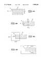
- FIG. 1Ashows the apparatus of the invention for three dimensional inspection.
- the apparatusincludes a camera 10 with a lens 12 and a reticle 20.
- the reticle 20includes a central region 22 for receiving a part 30 having a lead 50 for imaging by the camera.
- the camera 10is located below the central region 22 of the reticle 20 to receive an image of the part 30.
- the reticle 20includes optical elements 40 to provide additional perspectives of the part 30.
- the optical elements 40are attached to the reticle and are located around the central region 22 to provide multiple side views of the part 30 to the camera 10.
- the optical elements 40may comprise prisms.
- the optical elements 40may comprise mirrors.
- the camera 10is located to receive the image of part 30 and the additional perspectives provided by the optical elements 40.
- the camera 10includes a frame grabber board 18 to capture the image.
- the optics of the camera 10have a depth of focus encompassing the optical paths of the bottom view from the reticle 20 and the side views provided from the optical elements 40.
- the camera 10provides an image data output to a processor 14 to perform a three dimensional inspection as described in conjunction with FIGS. 2A and 2B.
- the processor 14may store the image in a memory 16.
- FIG. 1Bshows an example image acquired by the system shown in FIG. 1A.
- the image 60 obtained by the camera 10includes a bottom view 70 obtained by the view through the reticle 20.
- the bottom view 70shows an image of the part 32 and the leads 52, 54, 56, 58.
- the image 60further includes four side views 80, 82, 84, 86 obtained by the view through reticle 20 and reflected off the optical elements 40.
- the side views 80, 82, 84, 86show a respective side view of the part 32 and the corresponding leads 53, 55, 57, 59.
- lead 53 in side view 82corresponds to lead 52 in bottom view 70
- lead 55 in side view 84corresponds to lead 54 in bottom view 70, and so on.
- the inventionwill work with any number of side views. For example, one view may be used for inspecting a single row of leads. Two views may be used for two rows of leads.
- FIG. 1Cshows a method for three dimensional inspection of electronic leads from a single image.
- the methodstarts by providing a transparent reticle having a top surface in step 101.
- the methodplaces a part having electronic leads for inspection on a central portion of the top surface of the transparent reticle in step 102.
- the methodthen provides fixed optical elements for providing a side perspective of the part in step 103.
- the methodthen provides a camera located beneath the transparent reticle to receive an image of the part and the additional perspective provided by the fixed optical elements wherein the camera provides image data in step 104.
- the methodthen processes the image data with a computer to provide a three dimensional analysis of the part in step 105.
- FIGS. 2A and 2Bshow a flow diagram of the three dimensional inspection loop of the invention.
- the processbegins in step 110 by waiting for an inspection signal. When the signal changes state, the system initiates the inspection.
- the processorsends a command to a frame grabber board 18 to acquire an image of a part having leads from the camera in step 110.
- the camera 10captures an image comprising pixel values and the processor stores the image in memory.
- the imagecomprises information from both a bottom view of the part and a number of side views as shown in FIG. 1B.
- step 130the inspection system sends a signal to a part handler shown in FIGS. 9B, 9C and 9D that the part may be moved off the inspection reticle and that the next part may be put into place.
- the handlermay proceed with part placement while the inspection system processes the stored image data.
- the inspection systemprocesses the pixel values of the stored image in step 140 to find a rotation, X placement, and Y placement of the part relative to a center point found during calibration of the inspection system using the reticle mask shown in FIG. 4.
- the processordetermines these placement values finding points on four sides of the body of the part.
- the processoremploys a part definition file that contains measurement values for an ideal part.
- the processorcalculates an expected position for each lead of the part for the bottom view portion of the image.
- the processoremploys a search procedure on the image data to locate the position of the lead closest to the expected position in the bottom view.
- the processordetermines the lead's X and Y position in pixel values by finding edges on three sides of each lead with a sub-pixel image processing method as shown in FIGS. 10A-10D.
- the processorproceeds in step 160 to calculate an expected position of each lead in the side view of the image using the known position of the side view as determined during a calibration procedure as described in FIG. 6, and the position of the lead found in the bottom view.
- the processoremploys a sub-pixel procedure to determine the Z position of the lead in pixel values as described in greater detail in conjunction with FIG. 3A.
- the inspection loopflows to step 170 to determine a reference edge for each lead.
- the processordetermines a closest reference edge for each lead found in the side view.
- the juncture of the optical elements with the reticlemay serve as a reference edge.
- a reference edgemay be located on the transparent reticle.
- a virtual line of pixelsmay define the reference edge.
- the processorconverts pixel values to world locations for each lead in step 180 by using the pixel values and parameters determined during calibration. The world locations represent physical locations of the leads in relation to the reference edge.
- the processormeasures D S and D B dimensions and computes the Z dimension for each lead as further described in FIGS. 3A and 3B.
- the processorthen converts the world values to part values using the calculated part rotation, X placement, and Y placement in step 190 to define coordinates for the ideal part.
- the part valuesrepresent physical dimensions of the leads, such as lead length and lead width.
- these part valuesare compared to the ideal part values defined in the part file to calculate the deviation of each lead in three dimensions from the ideal location.
- the deviation valuesmay include: tip offset, skew, bent lead, width and coplanarity.
- the processorcompares these deviation values to predetermined thresholds with respect to the ideal part as defined in the part file in step 210 to provide an electronic lead inspection result.
- the predetermined tolerance valuesinclude pass tolerance values and fail tolerance values from industry standards. If the measurement values are less than or equal to the pass tolerance values, the processor assigns a pass result for the part. If the measurement values exceed the fail tolerance values, the processor assigns a fail result for the part.
- the processordesignates the part to be reworked.
- the processorreports the inspection result for the part in step 220, completing part inspection.
- the processthen returns to step 110 to await the next inspection signal.
- FIG. 3Ashows one method of the invention used to provide a three dimensional location of an object.
- the processoruses parameters determined from the calibration procedure as shown in FIG. 6 and a single image, the processor computes a three dimensional location.
- the processorlocates a reference line on the plane of the reticle 20 formed by the juncture of the optical element 40 with the plane of the reticle 20.
- Ray 300shows the optical path from reference edge 302 to the camera 10.
- Rays 300, 310 and 320are parallel with an axis of the camera 10.
- the processormeasures a distance D S as the distance between the reference edge 302 and the reflected view of the object 330 of the reflective face 312 of the optical element 40 as shown by optical path 310.
- the angle of the reflective face 312 and the reticle 20is 42°.
- the processordetermines the distance D B as the distance between the reference edge 302 and the view of the object 330 as indicated by the optical path 320.
- the processordetermines the distance Z 350 of the object 330 above the reticle plane.
- FIG. 7shows an example calculation of ⁇ during a calibration of the system.
- the processorcalculates the Z dimension using the equation:
- D Sdistance from the reference edge to the side view of the object
- D Bdistance from the reference edge to the bottom view of the object
- ⁇angle formed by the ray emanating from the object reflected by the optical element and received by the camera and the plane intersecting the object parallel to the reticle plane;
- FIG. 3Bshows an alternate method of the invention used to locate an object in three dimensions.
- the processor 14begins by locating a reference line 360 located on the reticle 20.
- an attachment of the optical element 40 with the reticle 20may provide the reference line 360.
- the processor 14determines an angle ⁇ 340 that is dependent upon the angle of the face 312 of the optical element 40 to the plane of the reticle 20.
- the angle ⁇ 340is determined by using two points 332 and 334.
- the processor 14determines a distance between points 332 and 334 by measuring the distance between two rays 333 and 335 that are parallel to the axis of the camera and extending downward from points 332 and 334.
- the processorthen examines the side view for the corresponding rays 370 and 372 received by the camera from the optical element 40. The distance between these two rays 370 and 372 in the side view is measured as ⁇ Z.
- ⁇is determined using the following equation: ##EQU1##
- Ris a measure of a distance from the intersection 382 of the face 312 of the optical element and the plane of the reticle 20 and the edge of the reference line 360.
- d Bdistance from a reference edge to the bottom view image of the object, which is the distance between rays 380 and 333;
- ⁇angle formed by the ray emanating from the object reflected by the fixed optical element and received by the camera and the plane intersecting the object parallel to the reticle plane;
- Roffset of reference line 360 and the intersection 382 between a reflective face of the optical element 40 and the transparent reticle 20.
- the processordetermines the height Z of an object above the upper surface of the reticle 20, using the following equation:
- the systemis calibrated by placing a pattern of calibration dots of known spacing and size on the reticle plane.
- FIG. 4shows one embodiment of a calibration dot pattern as viewed by the camera 10 with four side optical elements, fewer or more side optical elements may also be used.
- the camerareceives an image including a bottom view and four side views from the optical elements located on the reticle plane.
- the calibration dotsappear as direct images 410 and reflected images 420.
- FIG. 5shows the relationship between the direct image 410, the reflected image 420 and the reference edge 302 and the values of D S and D B .
- FIG. 6shows a method of the invention used to calibrate the system using the reticle mask 400.
- the methodbegins at step 600 by finding the calibration dots.
- the processorfinds a location and size of each dot visible directly from the bottom view and stores these results in memory. By comparing these results to known values stored in memory, the processor calculates the missing state values for the bottom calibration in steps 610 and 620. For example, in step 610 the processor determines camera distortion and roll angle and in step 620 the processor measures pixel width and height. These state values include pixel width and pixel height, pixel aspect ratio, optics distortion, and camera orientation with respect to the dot pattern. The processor then stores these results in memory. These results provide conversion factors for use during analysis to convert pixel values to world values.
- step 630the processor finds calibration dots visible in side views and reference edges. From these values, the processor determines the side view angles of the optical elements 40 in step 640 as shown in FIG. 7.
- the processorbegins by finding the missing state values for each side mirror calibration from the data. These include the position of the mirror to the reticle plane.
- the state valuesare stored in memory.
- FIG. 7shows how the system determines angle ⁇ 710 for the optical element 720 using D S and D B .
- the systemlocates a reference edge 730 and uses a reflected image 740 of the object 750 to determine a distance D S 760.
- D Bis determined by the distance from the reference edge 730 and the object 750.
- D Bdistance from a reference edge to the bottom view image of the object, whcih is the distance between rays 380 and 333;
- ⁇angle formed by the ray emanating from the object reflected by the fixed optical element and received by the camera and the plane intersecting the object parallel to the reticle plane.
- the inspection systemmay use these known values to determine the three dimensional location of an object in space.
- FIG. 8shows one embodiment of a method of the inspection system of the invention to determine a three dimensional position of an object in space.
- the methodbegins in step 800 by finding an object from the bottom view. Using a search method, the processor determines coordinates for the object. In one embodiment, the processor may employ a subpixel method as shown below in FIGS. 10A-10D to find a repeatable position. The method then proceeds to step 810 to find the object in a side view. The processor determines a subpixel location for the object in the same manner as for the bottom view. The processor finds a reference edge to a subpixel location in step 820, and then computes the observed values for D S and D B in step 830. From these known values, the processor may determine the x, y and z positions of the object in step 840.
- FIGS. 9A, 9B, 9C and 9Dshow alternate embodiments of the part holder, optical elements and illumination elements of the invention.
- a pedestal 910is attached to the central portion of the reticle 920.
- a part 900may be received on the pedestal 910 for analysis.
- Light sources 904provide illumination.
- An overhead light reflective diffuser 902is fixed above the reticle 920 and is positioned to receive illumination from the light sources 904 and provides diffused illumination for backlighting for the bottom view of part 900.
- the light sources 904comprise light arrays mounted on four sides of the reticle 920 to provide even illumination for each view.
- FIG. 9Ba vacuum holder 950 is used to suspend a part 900 above the top surface of the reticle 920.
- the vacuum holder 950suspends the part 900 substantially parallel to the face of the reticle 920.
- An overhead light reflective diffuser 906may be mounted on the vacuum holder 950 to receive light from the light sources 904.
- FIG. 9Cshows a vacuum holder 950 suspending a part 900 above a reticle 920 where a central portion 922 of the reticle has been cut out.
- the central portion 922 of the reticle 920has been cut out so that an inward face 942 of a prism 940 is substantially in line with the cut out portion of the reticle 920.
- FIG. 9Dshows a configuration similar to that shown in FIG. 9C, except that a mirror 952 is used in place of the prism 940.
- the processorbegins with known parameters determined from the bottom view to find an ideal location center for a lead 50 having a lead tip 51. Depending on the size of a part and other parameters such as lighting conditions, the ideal location center of the lead tip 51 may vary.
- the processordefines a region of interest, 11 ⁇ 19 pixels for example, around the ideal location center, shown in FIG. 10A as the coordinates nX, nY.
- the camerais a CCD camera that contains 1024 ⁇ 1024 pixels with a pixel representing approximately 1.6 thousandths of an inch of the lead. Other optical systems and camera types may be used without deviating from the spirit and scope of the invention.
- the size of the region of interestis chosen such that only one lead is contained in the region so that no other adjacent lead is contained in that region of interest.
- nWan expected width in pixels
- nLan expected length available of the lead 50 up to the body of the part
- an expected lead dimensionsare found as shown in FIG. 10A.
- a processorfinds a lead tip 51 by moving from the outside edge opposite the lead tip 51 toward the lead tip 51 one pixel at a time.
- the processordetermines the pixel having the maximum gradient to be the edge of the lead tip dT.
- the gradient for each pixelis found by subtracting a gray scale value of the pixel from the gray scale value of the next pixel.
- the processormay proceed by averaging groups of three or more pixels, as an example, rather than using individual pixels.
- the processordetermines the two lead tip edges' positions, dS 1 and dS 2 by moving five pixels, for example, into the lead along an axis parallel to the lead as defined by the ideal part. Then the method moves toward each of the side edges along a line perpendicular to the lead until a maximum gradient is found along the line.
- the pixel with the maximum gradient dS 1 and dS 2are defined as the side positions.
- the processorthen performs a subpixel operation as shown in FIG. 10B to find a more accurate seed position for a second subpixel operation.
- the processordefines a small 3 ⁇ 5 box around each position dT, dS 1 and dS 2 .
- the subpixel operationbegins on dT by averaging the three pixels in each column moving left to right and finding a more repeatable seed position dT. Likewise, more accurate seed positions dS 1 and dS 2 are found for the side locations moving from the non-lead edge into the lead while averaging the pixels in each row.
- the processordetermines tip position using the new seed point dTip and defining a large subpixel box of size 2 nW ⁇ 2nW where the tip point is centered left to right on dT, and centered top to bottom on (dS 1 and dS 2 )/2 as shown in FIG. 10C.
- the processormoves from left to right from a non-lead edge into the lead while averaging the pixels in each column to find dTip as the tip position.
- the side positionsare found using the seed positions dS 1 and dS 2 with a subpixel box of dimensions nL ⁇ nW.
- the seed positionis dS 1 and (dTip+nL/3).
- the seed positionis dS 2 and (dTip+nL/3).
- the processormoves towards the lead averaging the pixels in each row, and using the subpixel process shown below, determines a subpixel location of the lead edges as dSide 1 and dSide 2 .
- the width of the leadis then computed as dSide 1 -dSide 2 .
- subpixel edge detectionimplemented in the C language is shown below.
- an attachment of the optical element 1040which may comprise a prism, with the reticle 1004 may provide the reference line 1020.
- the attachmentwhich may be made with glue, may not provide a precise line.
- the reference line 1020is located on the reticle 1004 at the intersection of the transmissive face 1043 of the optical element 1040 and the reticle 1004.
- the width of the reference line 1020is chosen to be sufficiently narrow so as not to obscure the view of the part 1000, which may comprise a lead tip of the lead of an electronic component, from the camera 1015 off the reflective surface 1041 of the optical element 1040.
- the width of the reference line 1020may be selected to obscure the intersection of the transmissive face 1043 and the reticle 1004 and extend beyond the upper overhang of the optical element 1040. Imprecision may be introduced by an uneven line in the intersection of the transmissive face 1043 and the reticle 1004 caused by an adhesive used to attach the optical element 1040 to the reticle 1004. The width of the reference line allows for measurement without the imprecision introduced by the attachment of the optical element 1040 to the reticle 1004.
- FIG. 11Ashows an actual position of the part 1000 located a distance c 1002 which represents the distance above the plane of the reticle 1004 of the part 1000.
- the distance c 1002represents the distance in the z dimension of the part 1000 above the plane of the reticle 1004.
- Ray w 1006shows an optical path of a ray passing perpendicularly through the plane of the reticle 1004, reflecting off a back plane 1041 of the optical element 1040 and passing through the location of the part 1000.
- Ray u 1008shows the optical path of a ray passing upward perpendicularly through plane of the reticle 1004 reflecting off the back plane 1041 of the prism 1040 and passing through the point directly below part 1000.
- Ray u 1008is parallel to ray w 1006 and is separated by distance c from ray 1006 in the z dimension.
- the reflection of rays w 1006 and u 1008 off the back plane 1041 of the prism 1040form an angle b 1013 and angles of incidence a 1014 and reflection a 1016.
- Angle ⁇ 1012is defined as the angle formed at the intersection of ray u 1008 and plane of the reticle 1004.
- the distance t 1018is the distance from the part 1000 and the ray u 1008 where t 1018 is perpendicular to the ray u 1008.
- d B 1034is the distance along the x or y dimension from the leading edge of the reference line 1020 and the z projection intersection of the part 1000 and the plane of the reticle 1004.
- FIG. 11Bshows a reduced illustration of the relationships between angle ⁇ 1012, distance c 1002 and distance t 1018.
- the following equationsillustrate the relationships between these values. ##EQU4##
- FIG. 11Cshows a detailed illustration of relationships formed by reference line 1020 and the location of the part 1000.
- the distance sis the distance from the leading edge of the reference line 1020 and the ray u 1008 along a path parallel to the distance t 1018.
- the distance dp 1024is the sum of the two distances t 1018 and s 1022.
- Optical path 1026is formed by the reflection of a ray passing perpendicular through the plane of the reticle 1004 reflecting off the back plane 1041 of the prism 1040 and passing through the leading edge of the reference line 1020.
- the distance ds 1028is a measure of the distance in the plane of reticle 1004 of ray w 1006 from ray 1026 after reflection off the back plane 1041 of the prism 1040.
- the distance e 1030is a measure of the distance of the points of intersection of the ray w 1006 from ray 1026 on the back plane 1041 of the prism 1040.
- the angle D 1032is the angle of the back plane of the prism 1040 and the plane of the reticle 1004. Using these measures, the following relationship is determined.
- FIG. 11Dreduces the relationships of e 1030, angle a 1014, angle d 1032 and ds 1028. Therefore, ##EQU5##
- FIG. 11Eshows the relationships of the distance s 1022, ray u 1008, angle ⁇ 1012 and d B 1034. ##EQU6##
- FIG. 11Fwhich shows an illustration of the reduced relationship between the distance e 1030, d p 1024, angle a 1014 and angle b 1013
- an equation to solve for the position c 1002 of the part 1000 in the z-dimensionis derived as follows: ##EQU7##
Landscapes
- Engineering & Computer Science (AREA)
- Physics & Mathematics (AREA)
- General Physics & Mathematics (AREA)
- Theoretical Computer Science (AREA)
- Operations Research (AREA)
- Manufacturing & Machinery (AREA)
- Microelectronics & Electronic Packaging (AREA)
- Computer Vision & Pattern Recognition (AREA)
- Health & Medical Sciences (AREA)
- Quality & Reliability (AREA)
- Geometry (AREA)
- Life Sciences & Earth Sciences (AREA)
- Chemical & Material Sciences (AREA)
- Analytical Chemistry (AREA)
- Biochemistry (AREA)
- General Health & Medical Sciences (AREA)
- Immunology (AREA)
- Pathology (AREA)
- Length Measuring Devices By Optical Means (AREA)
- Image Processing (AREA)
Abstract
Description
Z=D.sub.S tan (45°-θ/2)-(D.sub.B -D.sub.S) tan θ
Z=(d.sub.S +R) tan (45°-θ/2)-(d.sub.B -d.sub.S) tan θ.
______________________________________void IML.sub.-- FindHorzEdge(int nXseed,int nYseed, int nWidth,int nLength, double * dEdge)int nXstart = nXseed - (nLength - 1) /2;int nYstart = nYseed - (nWidth - 1) /2;int nXstop = nXstart + nLength;int nYstop = nYstart + nWidth;int *nArray MAX.sub.-- LENGTH!;double d1, d2, d3;double dL = nLength;double dM1 = 0.0;double dM2 = 0.0;double dM3 = 0.0;double dM11;for (int x=nXstart;x<nXstop;x++){d1 = 0.0;nArray x-nXstart! = 0;for (int y=nYstart;y<nYstop;y++){nArray x-nXstart! += GET.sub.-- PIXEL(x,y);}d1 = nArray x-nXstart!;d2 = d1 + d1;d3 = d2 + d1;dM1 += d1;dM2 += d2;dM3 += d3;}dM1 /= dL;dM2 /= dL;dM3 /= dL;dM11 = dM1 + dM1;double dS1 = dM3 - dM1 * (3.0 *dM2-2.0*dM11);double dS2 = (dM2 - dM11) * sqrt(fabs (dM2-dM11));if (dS2 == 0.0) dS2 - 1.0;double dS3 = dS1 / dS2;double dP = 0.5-dS3/(2.0*sqrt(4.0 + dS3 * dS3));double dE = dP*dL + 0.5;if (nArray 0! > nArray nLength - 1!)*dEdge = (double)nXseed - (double) (nLength+1)/2.0 + dE;else*dEdge = (double)nXseed + (double) (nLength+1)/2.0 - dE;} © 1997 Scanner Technologies, Inc.______________________________________dp=t+s
t=dp-s.
sin θ=S/d.sub.B
Claims (33)
Z=D.sub.S tan (45°-θ/2)-(D.sub.B -D.sub.S) tan θ
Z=(d.sub.S +R) tan (45°-θ/2)-(d.sub.B -d.sub.S) tan θ
Priority Applications (4)
| Application Number | Priority Date | Filing Date | Title |
|---|---|---|---|
| US08/955,198US5909285A (en) | 1997-05-05 | 1997-10-21 | Three dimensional inspection system |
| EP98953766AEP1025418A4 (en) | 1997-10-21 | 1998-10-20 | Three-dimensional inspection system |
| JP2000517250AJP2001521140A (en) | 1997-10-21 | 1998-10-20 | 3D inspection system |
| PCT/US1998/022151WO1999020977A1 (en) | 1997-10-21 | 1998-10-20 | Three-dimensional inspection system |
Applications Claiming Priority (2)
| Application Number | Priority Date | Filing Date | Title |
|---|---|---|---|
| US08/850,473US6055054A (en) | 1997-05-05 | 1997-05-05 | Three dimensional inspection system |
| US08/955,198US5909285A (en) | 1997-05-05 | 1997-10-21 | Three dimensional inspection system |
Related Parent Applications (1)
| Application Number | Title | Priority Date | Filing Date |
|---|---|---|---|
| US08/850,473Continuation-In-PartUS6055054A (en) | 1997-05-05 | 1997-05-05 | Three dimensional inspection system |
Publications (1)
| Publication Number | Publication Date |
|---|---|
| US5909285Atrue US5909285A (en) | 1999-06-01 |
Family
ID=25496516
Family Applications (1)
| Application Number | Title | Priority Date | Filing Date |
|---|---|---|---|
| US08/955,198Expired - LifetimeUS5909285A (en) | 1997-05-05 | 1997-10-21 | Three dimensional inspection system |
Country Status (4)
| Country | Link |
|---|---|
| US (1) | US5909285A (en) |
| EP (1) | EP1025418A4 (en) |
| JP (1) | JP2001521140A (en) |
| WO (1) | WO1999020977A1 (en) |
Cited By (39)
| Publication number | Priority date | Publication date | Assignee | Title |
|---|---|---|---|---|
| US6061466A (en)* | 1995-12-26 | 2000-05-09 | Kabushiki Kaisha Toshiba | Apparatus and method for inspecting an LSI device in an assembling process, capable of detecting connection failure of individual flexible leads |
| US6088108A (en)* | 1998-08-27 | 2000-07-11 | Hewlett-Packard Company | Leaded components inspection system |
| US6141040A (en)* | 1996-01-09 | 2000-10-31 | Agilent Technologies, Inc. | Measurement and inspection of leads on integrated circuit packages |
| SG84530A1 (en)* | 1998-05-21 | 2001-11-20 | Agilent Technologies Inc | Cross optical axis inspection system for integrated circuits |
| WO2002044651A1 (en)* | 2000-11-28 | 2002-06-06 | Semiconductor Technologies & Instruments, Inc. | Three dimensional lead inspection system |
| EP1220596A1 (en)* | 2000-12-29 | 2002-07-03 | Icos Vision Systems N.V. | A method and an apparatus for measuring positions of contact elements of an electronic component |
| US20020135757A1 (en)* | 2001-01-02 | 2002-09-26 | Robotic Vision Systems, Inc. | LCC device inspection module |
| WO2002017357A3 (en)* | 2000-08-22 | 2002-11-28 | Agilent Technologies Inc | Three dimensional inspection of leaded ics |
| US6522777B1 (en) | 1998-07-08 | 2003-02-18 | Ppt Vision, Inc. | Combined 3D- and 2D-scanning machine-vision system and method |
| US6573987B2 (en)* | 2001-01-02 | 2003-06-03 | Robotic Vision Systems, Inc. | LCC device inspection module |
| US6628380B1 (en)* | 2000-07-03 | 2003-09-30 | International Business Machines Corporation | Appearance inspecting jig for small parts and inspecting method employing the same jig |
| WO2004001285A3 (en)* | 2002-06-21 | 2004-04-29 | Pressco Tech Inc | Patterned illumination method and apparatus for machine vision systems |
| WO2004079427A1 (en)* | 2003-03-07 | 2004-09-16 | Ismeca Semiconductor Holding Sa | Optical device and inspection module |
| US6813016B2 (en) | 2002-03-15 | 2004-11-02 | Ppt Vision, Inc. | Co-planarity and top-down examination method and optical module for electronic leaded components |
| US20040234122A1 (en)* | 2001-07-30 | 2004-11-25 | Nobuo Kochi | Surface shape measurement apparatus, surface shape measurement method, surface state graphic apparatus |
| US6829371B1 (en)* | 2000-04-29 | 2004-12-07 | Cognex Corporation | Auto-setup of a video safety curtain system |
| US6915007B2 (en) | 1998-01-16 | 2005-07-05 | Elwin M. Beaty | Method and apparatus for three dimensional inspection of electronic components |
| US6915006B2 (en) | 1998-01-16 | 2005-07-05 | Elwin M. Beaty | Method and apparatus for three dimensional inspection of electronic components |
| US6956963B2 (en) | 1998-07-08 | 2005-10-18 | Ismeca Europe Semiconductor Sa | Imaging for a machine-vision system |
| EP1475748A3 (en)* | 2003-05-08 | 2006-05-10 | Siemens Aktiengesellschaft | Method and apparatus for acquisition of objects |
| US20060118742A1 (en)* | 2004-12-06 | 2006-06-08 | Richard Levenson | Systems and methods for in-vivo optical imaging and measurement |
| US7142301B2 (en) | 1999-07-08 | 2006-11-28 | Ppt Vision | Method and apparatus for adjusting illumination angle |
| US20070076196A1 (en)* | 2005-08-09 | 2007-04-05 | Powerchip Semiconductor Corp. | System and method for visual inspection of wafer |
| US7353954B1 (en) | 1998-07-08 | 2008-04-08 | Charles A. Lemaire | Tray flipper and method for parts inspection |
| US7508974B2 (en) | 1998-01-16 | 2009-03-24 | Scanner Technologies Corporation | Electronic component products and method of manufacturing electronic component products |
| US7734102B2 (en) | 2005-05-11 | 2010-06-08 | Optosecurity Inc. | Method and system for screening cargo containers |
| US7899232B2 (en) | 2006-05-11 | 2011-03-01 | Optosecurity Inc. | Method and apparatus for providing threat image projection (TIP) in a luggage screening system, and luggage screening system implementing same |
| US7991242B2 (en) | 2005-05-11 | 2011-08-02 | Optosecurity Inc. | Apparatus, method and system for screening receptacles and persons, having image distortion correction functionality |
| US20130120557A1 (en)* | 2011-11-14 | 2013-05-16 | Microscan Systems, Inc. | Part inspection system |
| US8494210B2 (en) | 2007-03-30 | 2013-07-23 | Optosecurity Inc. | User interface for use in security screening providing image enhancement capabilities and apparatus for implementing same |
| JP2015152510A (en)* | 2014-02-18 | 2015-08-24 | 株式会社東芝 | Lead frame shape inspection apparatus and lead frame distance measuring method |
| TWI547684B (en)* | 2014-05-21 | 2016-09-01 | 東和股份有限公司 | Device for photographing side of electronic component package |
| WO2016195726A1 (en)* | 2015-06-05 | 2016-12-08 | Kla-Tencor Corporation | Apparatus, method and computer program product for inspection of at least side faces of semiconductor devices |
| US9632206B2 (en) | 2011-09-07 | 2017-04-25 | Rapiscan Systems, Inc. | X-ray inspection system that integrates manifest data with imaging/detection processing |
| US20180188184A1 (en)* | 2015-08-26 | 2018-07-05 | Abb Schweiz Ag | Object multi-perspective inspection apparatus and method therefor |
| US10302807B2 (en) | 2016-02-22 | 2019-05-28 | Rapiscan Systems, Inc. | Systems and methods for detecting threats and contraband in cargo |
| CN111551551A (en)* | 2020-05-12 | 2020-08-18 | 德奥福臻越智能机器人(杭州)有限公司 | Vehicle door plate detection system and detection method |
| US10871456B2 (en)* | 2019-02-07 | 2020-12-22 | Kabushiki Kaisha Toshiba | Semiconductor inspection system and semiconductor inspection apparatus |
| CN113758420A (en)* | 2021-09-08 | 2021-12-07 | 深圳市龙图光电有限公司 | Mask plate auxiliary static image measuring device and mask plate static image measuring system |
Families Citing this family (6)
| Publication number | Priority date | Publication date | Assignee | Title |
|---|---|---|---|---|
| WO2001004567A2 (en)* | 1999-07-13 | 2001-01-18 | Beaty, Elwin, M. | Method and apparatus for three dimensional inspection of electronic components |
| US7289646B2 (en)* | 2003-06-30 | 2007-10-30 | Weyerhaeuser Company | Method and system for simultaneously imaging multiple views of a plant embryo |
| US7384497B2 (en) | 2004-06-29 | 2008-06-10 | Weyerhaeuser Company | Process for encapsulation of cellulose based substrates using electromagnetic radiation heating |
| AT516417B1 (en)* | 2014-10-29 | 2018-10-15 | Zkw Group Gmbh | Limitation for placing electronic components on a surface |
| CN106442544B (en)* | 2016-10-18 | 2018-11-20 | 凌云光技术集团有限责任公司 | Omnidirectional imaging system |
| CN106767537B (en)* | 2017-03-20 | 2019-03-01 | 重庆市光学机械研究所 | A kind of monocular various dimensions profile scan device |
Citations (19)
| Publication number | Priority date | Publication date | Assignee | Title |
|---|---|---|---|---|
| US4638471A (en)* | 1985-06-10 | 1987-01-20 | U.S. Philips Corporation | Optical scanning unit comprising a translational-position and angular-position detection system for an electro-magnetically suspended objective |
| US4825394A (en)* | 1985-05-07 | 1989-04-25 | General Dynamics Corporation | Vision metrology system |
| US4886958A (en)* | 1988-03-25 | 1989-12-12 | Texas Instruments Incorporated | Autofocus system for scanning laser inspector or writer |
| US4943722A (en)* | 1986-09-24 | 1990-07-24 | Trialsite Limited | Charged particle beam scanning apparatus |
| WO1991012489A1 (en)* | 1990-02-09 | 1991-08-22 | Abos Automation, Bildverarbeitung Optische Systeme Gmbh | Process and device for automatic monitoring of space-shape data in the manufacture of semiconductor components |
| US5095447A (en)* | 1988-03-25 | 1992-03-10 | Texas Instruments Incorporated | Color overlay of scanned and reference images for display |
| WO1992007250A1 (en)* | 1990-10-11 | 1992-04-30 | Abos Automation, Bildverarbeitung Optische System Gmbh | Process and device for automated monitoring of the manufacture of semiconductor components |
| US5113581A (en)* | 1989-12-19 | 1992-05-19 | Matsushita Electric Industrial Co., Ltd. | Outer lead bonding head and method of bonding outer lead |
| US5133601A (en)* | 1991-06-12 | 1992-07-28 | Wyko Corporation | Rough surface profiler and method |
| US5140643A (en)* | 1989-12-28 | 1992-08-18 | Matsushita Electric Industries Co., Ltd. | Part mounting apparatus with single viewing camera viewing part from different directions |
| US5173796A (en)* | 1991-05-20 | 1992-12-22 | Palm Steven G | Three dimensional scanning system |
| US5204734A (en)* | 1991-06-12 | 1993-04-20 | Wyko Corporation | Rough surface profiler and method |
| US5307149A (en)* | 1992-08-14 | 1994-04-26 | Elwin M. Beaty | Method and apparatus for zero force part placement |
| US5420691A (en)* | 1991-03-15 | 1995-05-30 | Matsushita Electric Industrial Co., Ltd. | Electric component observation system |
| US5430548A (en)* | 1992-02-06 | 1995-07-04 | Hitachi, Ltd. | Method and apparatus for pattern detection |
| US5452080A (en)* | 1993-06-04 | 1995-09-19 | Sony Corporation | Image inspection apparatus and method |
| US5563702A (en)* | 1991-08-22 | 1996-10-08 | Kla Instruments Corporation | Automated photomask inspection apparatus and method |
| US5563703A (en)* | 1994-06-20 | 1996-10-08 | Motorola, Inc. | Lead coplanarity inspection apparatus and method thereof |
| US5574668A (en)* | 1995-02-22 | 1996-11-12 | Beaty; Elwin M. | Apparatus and method for measuring ball grid arrays |
Family Cites Families (6)
| Publication number | Priority date | Publication date | Assignee | Title |
|---|---|---|---|---|
| US4959898A (en)* | 1990-05-22 | 1990-10-02 | Emhart Industries, Inc. | Surface mount machine with lead coplanarity verifier |
| JPH05340733A (en)* | 1992-06-05 | 1993-12-21 | Asahi Kasei Micro Syst Kk | Semiconductor device inspecting device |
| JP3381341B2 (en)* | 1993-01-26 | 2003-02-24 | ソニー株式会社 | Apparatus and method for inspecting appearance of semiconductor device |
| WO1996022673A1 (en)* | 1995-12-11 | 1996-07-25 | Qtec Industrie-Automation Gmbh | Process and device for three-dimensional noncontact measurement of the geometry of leads on semiconductor devices |
| JP3296705B2 (en)* | 1995-12-18 | 2002-07-02 | 三洋電機株式会社 | Generating device for standard data for component recognition |
| US6055054A (en)* | 1997-05-05 | 2000-04-25 | Beaty; Elwin M. | Three dimensional inspection system |
- 1997
- 1997-10-21USUS08/955,198patent/US5909285A/ennot_activeExpired - Lifetime
- 1998
- 1998-10-20WOPCT/US1998/022151patent/WO1999020977A1/enactiveApplication Filing
- 1998-10-20EPEP98953766Apatent/EP1025418A4/ennot_activeWithdrawn
- 1998-10-20JPJP2000517250Apatent/JP2001521140A/enactivePending
Patent Citations (21)
| Publication number | Priority date | Publication date | Assignee | Title |
|---|---|---|---|---|
| US4825394A (en)* | 1985-05-07 | 1989-04-25 | General Dynamics Corporation | Vision metrology system |
| US4638471A (en)* | 1985-06-10 | 1987-01-20 | U.S. Philips Corporation | Optical scanning unit comprising a translational-position and angular-position detection system for an electro-magnetically suspended objective |
| US4943722A (en)* | 1986-09-24 | 1990-07-24 | Trialsite Limited | Charged particle beam scanning apparatus |
| US4886958A (en)* | 1988-03-25 | 1989-12-12 | Texas Instruments Incorporated | Autofocus system for scanning laser inspector or writer |
| US5095447A (en)* | 1988-03-25 | 1992-03-10 | Texas Instruments Incorporated | Color overlay of scanned and reference images for display |
| US5113581A (en)* | 1989-12-19 | 1992-05-19 | Matsushita Electric Industrial Co., Ltd. | Outer lead bonding head and method of bonding outer lead |
| US5140643A (en)* | 1989-12-28 | 1992-08-18 | Matsushita Electric Industries Co., Ltd. | Part mounting apparatus with single viewing camera viewing part from different directions |
| WO1991012489A1 (en)* | 1990-02-09 | 1991-08-22 | Abos Automation, Bildverarbeitung Optische Systeme Gmbh | Process and device for automatic monitoring of space-shape data in the manufacture of semiconductor components |
| WO1992007250A1 (en)* | 1990-10-11 | 1992-04-30 | Abos Automation, Bildverarbeitung Optische System Gmbh | Process and device for automated monitoring of the manufacture of semiconductor components |
| US5420691A (en)* | 1991-03-15 | 1995-05-30 | Matsushita Electric Industrial Co., Ltd. | Electric component observation system |
| US5173796A (en)* | 1991-05-20 | 1992-12-22 | Palm Steven G | Three dimensional scanning system |
| US5276546A (en)* | 1991-05-20 | 1994-01-04 | Butch Beaty | Three dimensional scanning system |
| US5204734A (en)* | 1991-06-12 | 1993-04-20 | Wyko Corporation | Rough surface profiler and method |
| US5355221A (en)* | 1991-06-12 | 1994-10-11 | Wyko Corporation | Rough surface profiler and method |
| US5133601A (en)* | 1991-06-12 | 1992-07-28 | Wyko Corporation | Rough surface profiler and method |
| US5563702A (en)* | 1991-08-22 | 1996-10-08 | Kla Instruments Corporation | Automated photomask inspection apparatus and method |
| US5430548A (en)* | 1992-02-06 | 1995-07-04 | Hitachi, Ltd. | Method and apparatus for pattern detection |
| US5307149A (en)* | 1992-08-14 | 1994-04-26 | Elwin M. Beaty | Method and apparatus for zero force part placement |
| US5452080A (en)* | 1993-06-04 | 1995-09-19 | Sony Corporation | Image inspection apparatus and method |
| US5563703A (en)* | 1994-06-20 | 1996-10-08 | Motorola, Inc. | Lead coplanarity inspection apparatus and method thereof |
| US5574668A (en)* | 1995-02-22 | 1996-11-12 | Beaty; Elwin M. | Apparatus and method for measuring ball grid arrays |
Cited By (79)
| Publication number | Priority date | Publication date | Assignee | Title |
|---|---|---|---|---|
| US6061466A (en)* | 1995-12-26 | 2000-05-09 | Kabushiki Kaisha Toshiba | Apparatus and method for inspecting an LSI device in an assembling process, capable of detecting connection failure of individual flexible leads |
| US6141040A (en)* | 1996-01-09 | 2000-10-31 | Agilent Technologies, Inc. | Measurement and inspection of leads on integrated circuit packages |
| US7508974B2 (en) | 1998-01-16 | 2009-03-24 | Scanner Technologies Corporation | Electronic component products and method of manufacturing electronic component products |
| US6915006B2 (en) | 1998-01-16 | 2005-07-05 | Elwin M. Beaty | Method and apparatus for three dimensional inspection of electronic components |
| US6915007B2 (en) | 1998-01-16 | 2005-07-05 | Elwin M. Beaty | Method and apparatus for three dimensional inspection of electronic components |
| SG84530A1 (en)* | 1998-05-21 | 2001-11-20 | Agilent Technologies Inc | Cross optical axis inspection system for integrated circuits |
| US6956963B2 (en) | 1998-07-08 | 2005-10-18 | Ismeca Europe Semiconductor Sa | Imaging for a machine-vision system |
| US20090180679A1 (en)* | 1998-07-08 | 2009-07-16 | Charles A. Lemaire | Method and apparatus for parts manipulation, inspection, and replacement |
| US7353954B1 (en) | 1998-07-08 | 2008-04-08 | Charles A. Lemaire | Tray flipper and method for parts inspection |
| US7719670B2 (en) | 1998-07-08 | 2010-05-18 | Charles A. Lemaire | Parts manipulation, inspection, and replacement system and method |
| US6522777B1 (en) | 1998-07-08 | 2003-02-18 | Ppt Vision, Inc. | Combined 3D- and 2D-scanning machine-vision system and method |
| US20090073427A1 (en)* | 1998-07-08 | 2009-03-19 | Charles A. Lemaire | Parts manipulation, inspection, and replacement system and method |
| US7773209B2 (en) | 1998-07-08 | 2010-08-10 | Charles A. Lemaire | Method and apparatus for parts manipulation, inspection, and replacement |
| US20090078620A1 (en)* | 1998-07-08 | 2009-03-26 | Charles A. Lemaire | Tray flipper, tray, and method for parts inspection |
| US8408379B2 (en) | 1998-07-08 | 2013-04-02 | Charles A. Lemaire | Parts manipulation, inspection, and replacement |
| US8056700B2 (en) | 1998-07-08 | 2011-11-15 | Charles A. Lemaire | Tray flipper, tray, and method for parts inspection |
| US8286780B2 (en) | 1998-07-08 | 2012-10-16 | Charles A. Lemaire | Parts manipulation, inspection, and replacement system and method |
| US6088108A (en)* | 1998-08-27 | 2000-07-11 | Hewlett-Packard Company | Leaded components inspection system |
| SG72860A1 (en)* | 1998-08-27 | 2001-03-20 | Agilent Technologies Inc | Leaded components inspection system |
| US7557920B2 (en) | 1999-07-08 | 2009-07-07 | Lebens Gary A | Method and apparatus for auto-adjusting illumination |
| US7142301B2 (en) | 1999-07-08 | 2006-11-28 | Ppt Vision | Method and apparatus for adjusting illumination angle |
| US20070206183A1 (en)* | 1999-07-08 | 2007-09-06 | Ppt Vision, Inc. | Method and apparatus for auto-adjusting illumination |
| US6829371B1 (en)* | 2000-04-29 | 2004-12-07 | Cognex Corporation | Auto-setup of a video safety curtain system |
| US6628380B1 (en)* | 2000-07-03 | 2003-09-30 | International Business Machines Corporation | Appearance inspecting jig for small parts and inspecting method employing the same jig |
| WO2002017357A3 (en)* | 2000-08-22 | 2002-11-28 | Agilent Technologies Inc | Three dimensional inspection of leaded ics |
| WO2002044651A1 (en)* | 2000-11-28 | 2002-06-06 | Semiconductor Technologies & Instruments, Inc. | Three dimensional lead inspection system |
| US6567161B1 (en)* | 2000-11-28 | 2003-05-20 | Asti Holdings Limited | Three dimensional lead inspection system |
| EP1220596A1 (en)* | 2000-12-29 | 2002-07-03 | Icos Vision Systems N.V. | A method and an apparatus for measuring positions of contact elements of an electronic component |
| US20040085549A1 (en)* | 2000-12-29 | 2004-05-06 | Carl Smets | Method and an apparatus for measuring positions of contact elements of an electronic component |
| WO2002054849A1 (en)* | 2000-12-29 | 2002-07-11 | Icos Vision Systems N.V. | A method and an apparatus for measuring positions of contact elements of an electronic component |
| US7423743B2 (en) | 2000-12-29 | 2008-09-09 | Icos Vision Systems Nv | Method and an apparatus for measuring positions of contact elements of an electronic component |
| US6573987B2 (en)* | 2001-01-02 | 2003-06-03 | Robotic Vision Systems, Inc. | LCC device inspection module |
| US20020135757A1 (en)* | 2001-01-02 | 2002-09-26 | Robotic Vision Systems, Inc. | LCC device inspection module |
| US20040234122A1 (en)* | 2001-07-30 | 2004-11-25 | Nobuo Kochi | Surface shape measurement apparatus, surface shape measurement method, surface state graphic apparatus |
| US7206080B2 (en)* | 2001-07-30 | 2007-04-17 | Topcon Corporation | Surface shape measurement apparatus, surface shape measurement method, surface state graphic apparatus |
| US20040227959A1 (en)* | 2002-03-15 | 2004-11-18 | Quist Bradley L. | Co-planarity examination method and optical module for electronic components |
| US7012682B2 (en) | 2002-03-15 | 2006-03-14 | Charles A. Lemaire | Co-planarity examination method and optical module for electronic components |
| US7154596B2 (en) | 2002-03-15 | 2006-12-26 | Quist Bradley L | Method and apparatus for backlighting and imaging multiple views of isolated features of an object |
| US20060152741A1 (en)* | 2002-03-15 | 2006-07-13 | Quist Bradley L | Method and apparatus for backlighting and imaging multiple views of isolated features of an object |
| US6813016B2 (en) | 2002-03-15 | 2004-11-02 | Ppt Vision, Inc. | Co-planarity and top-down examination method and optical module for electronic leaded components |
| WO2004001285A3 (en)* | 2002-06-21 | 2004-04-29 | Pressco Tech Inc | Patterned illumination method and apparatus for machine vision systems |
| US8598557B2 (en) | 2002-06-21 | 2013-12-03 | Pressco Technology Inc. | Method and apparatus for providing patterned illumination fields for machine vision systems |
| US20060091333A1 (en)* | 2002-06-21 | 2006-05-04 | Cochran Don W | Patterned illumination method and apparatus for machine vision systems |
| US20050185181A1 (en)* | 2003-03-07 | 2005-08-25 | Ismeca Semiconductor Holding Sa | Optical device and inspection module |
| US7283235B2 (en) | 2003-03-07 | 2007-10-16 | Ismeca Semiconductor Holding Sa | Optical device and inspection module |
| WO2004079427A1 (en)* | 2003-03-07 | 2004-09-16 | Ismeca Semiconductor Holding Sa | Optical device and inspection module |
| EP1475748A3 (en)* | 2003-05-08 | 2006-05-10 | Siemens Aktiengesellschaft | Method and apparatus for acquisition of objects |
| US11806111B2 (en) | 2004-12-06 | 2023-11-07 | Cambridge Research & Instrumentation, Inc. | Systems and methods for in-vivo optical imaging and measurement |
| US7873407B2 (en)* | 2004-12-06 | 2011-01-18 | Cambridge Research & Instrumentation, Inc. | Systems and methods for in-vivo optical imaging and measurement |
| US20060118742A1 (en)* | 2004-12-06 | 2006-06-08 | Richard Levenson | Systems and methods for in-vivo optical imaging and measurement |
| US20060119865A1 (en)* | 2004-12-06 | 2006-06-08 | Hoyt Clifford C | Systems and methods for in-vivo optical imaging and measurement |
| US8103331B2 (en)* | 2004-12-06 | 2012-01-24 | Cambridge Research & Instrumentation, Inc. | Systems and methods for in-vivo optical imaging and measurement |
| US7734102B2 (en) | 2005-05-11 | 2010-06-08 | Optosecurity Inc. | Method and system for screening cargo containers |
| US7991242B2 (en) | 2005-05-11 | 2011-08-02 | Optosecurity Inc. | Apparatus, method and system for screening receptacles and persons, having image distortion correction functionality |
| US20070076196A1 (en)* | 2005-08-09 | 2007-04-05 | Powerchip Semiconductor Corp. | System and method for visual inspection of wafer |
| US7899232B2 (en) | 2006-05-11 | 2011-03-01 | Optosecurity Inc. | Method and apparatus for providing threat image projection (TIP) in a luggage screening system, and luggage screening system implementing same |
| US8494210B2 (en) | 2007-03-30 | 2013-07-23 | Optosecurity Inc. | User interface for use in security screening providing image enhancement capabilities and apparatus for implementing same |
| US10830920B2 (en) | 2011-09-07 | 2020-11-10 | Rapiscan Systems, Inc. | Distributed analysis X-ray inspection methods and systems |
| US10509142B2 (en) | 2011-09-07 | 2019-12-17 | Rapiscan Systems, Inc. | Distributed analysis x-ray inspection methods and systems |
| US12174334B2 (en) | 2011-09-07 | 2024-12-24 | Rapiscan Systems, Inc. | Distributed analysis X-ray inspection methods and systems |
| US9632206B2 (en) | 2011-09-07 | 2017-04-25 | Rapiscan Systems, Inc. | X-ray inspection system that integrates manifest data with imaging/detection processing |
| US11099294B2 (en) | 2011-09-07 | 2021-08-24 | Rapiscan Systems, Inc. | Distributed analysis x-ray inspection methods and systems |
| US10422919B2 (en) | 2011-09-07 | 2019-09-24 | Rapiscan Systems, Inc. | X-ray inspection system that integrates manifest data with imaging/detection processing |
| US20130120557A1 (en)* | 2011-11-14 | 2013-05-16 | Microscan Systems, Inc. | Part inspection system |
| JP2015152510A (en)* | 2014-02-18 | 2015-08-24 | 株式会社東芝 | Lead frame shape inspection apparatus and lead frame distance measuring method |
| TWI547684B (en)* | 2014-05-21 | 2016-09-01 | 東和股份有限公司 | Device for photographing side of electronic component package |
| US10190994B2 (en) | 2015-06-05 | 2019-01-29 | Kla-Tencor Corporation | Apparatus, method and computer program product for inspection of at least side faces of semiconductor devices |
| EP3281219A4 (en)* | 2015-06-05 | 2018-12-19 | KLA - Tencor Corporation | Apparatus, method and computer program product for inspection of at least side faces of semiconductor devices |
| WO2016195726A1 (en)* | 2015-06-05 | 2016-12-08 | Kla-Tencor Corporation | Apparatus, method and computer program product for inspection of at least side faces of semiconductor devices |
| US10488346B2 (en)* | 2015-08-26 | 2019-11-26 | Abb Schweiz Ag | Object multi-perspective inspection apparatus and method therefor |
| US10788429B2 (en) | 2015-08-26 | 2020-09-29 | Abb Schweiz Ag | Object multi-perspective inspection apparatus and method therefor |
| US20180188184A1 (en)* | 2015-08-26 | 2018-07-05 | Abb Schweiz Ag | Object multi-perspective inspection apparatus and method therefor |
| US10768338B2 (en) | 2016-02-22 | 2020-09-08 | Rapiscan Systems, Inc. | Systems and methods for detecting threats and contraband in cargo |
| US10302807B2 (en) | 2016-02-22 | 2019-05-28 | Rapiscan Systems, Inc. | Systems and methods for detecting threats and contraband in cargo |
| US11287391B2 (en) | 2016-02-22 | 2022-03-29 | Rapiscan Systems, Inc. | Systems and methods for detecting threats and contraband in cargo |
| US10871456B2 (en)* | 2019-02-07 | 2020-12-22 | Kabushiki Kaisha Toshiba | Semiconductor inspection system and semiconductor inspection apparatus |
| CN111551551A (en)* | 2020-05-12 | 2020-08-18 | 德奥福臻越智能机器人(杭州)有限公司 | Vehicle door plate detection system and detection method |
| CN113758420A (en)* | 2021-09-08 | 2021-12-07 | 深圳市龙图光电有限公司 | Mask plate auxiliary static image measuring device and mask plate static image measuring system |
| CN113758420B (en)* | 2021-09-08 | 2022-06-14 | 深圳市龙图光电有限公司 | Mask plate auxiliary static image measuring device and mask plate static image measuring system |
Also Published As
| Publication number | Publication date |
|---|---|
| EP1025418A4 (en) | 2006-09-20 |
| EP1025418A1 (en) | 2000-08-09 |
| JP2001521140A (en) | 2001-11-06 |
| WO1999020977A1 (en) | 1999-04-29 |
Similar Documents
| Publication | Publication Date | Title |
|---|---|---|
| US5909285A (en) | Three dimensional inspection system | |
| US6055054A (en) | Three dimensional inspection system | |
| US6072898A (en) | Method and apparatus for three dimensional inspection of electronic components | |
| US5510833A (en) | Method and apparatus for transforming coordinate systems in an automated video monitor alignment system | |
| US5276546A (en) | Three dimensional scanning system | |
| US6141040A (en) | Measurement and inspection of leads on integrated circuit packages | |
| US5459794A (en) | Method and apparatus for measuring the size of a circuit or wiring pattern formed on a hybrid integrated circuit chip and a wiring board respectively | |
| US7085411B2 (en) | Method of manufacturing electronic components including a method for three dimensional inspection | |
| US7653237B2 (en) | Method of manufacturing ball array devices using an inspection apparatus having two or more cameras and ball array devices produced according to the method | |
| JP2003130621A (en) | Method and system for measuring three-dimensional shape | |
| JP2003522347A (en) | Automatic inspection system using stereo images | |
| US20020034324A1 (en) | Method and apparatus for three dimensional inspection of electronic components | |
| US5402505A (en) | Semiconductor device lead inspection system | |
| EP0781991A2 (en) | Improvements in or relating to semiconductor devices | |
| EP1218688B1 (en) | Method and apparatus for three dimensional inspection of electronic components | |
| CA2013337C (en) | Optical radius gauge | |
| JPH01242905A (en) | Method for measuring actual size of visual device |
Legal Events
| Date | Code | Title | Description |
|---|---|---|---|
| AS | Assignment | Owner name:ELWIN M. BEATY, MINNESOTA Free format text:ASSIGNMENT OF ASSIGNORS INTEREST;ASSIGNOR:MORK, DAVID P.;REEL/FRAME:009236/0221 Effective date:19980520 | |
| STCF | Information on status: patent grant | Free format text:PATENTED CASE | |
| FPAY | Fee payment | Year of fee payment:4 | |
| REMI | Maintenance fee reminder mailed | ||
| AS | Assignment | Owner name:SCANNER TECHNOLOGIES CORPORATION, MINNESOTA Free format text:ASSIGNMENT OF ASSIGNORS INTEREST;ASSIGNOR:BEATY, ELWIN M.;REEL/FRAME:017344/0751 Effective date:20060303 | |
| FPAY | Fee payment | Year of fee payment:8 | |
| AS | Assignment | Owner name:MORK, DAVID P., ARIZONA Free format text:SECURITY AGREEMENT;ASSIGNOR:SCANNER TECHNOLOGIES CORPORATION;REEL/FRAME:020031/0478 Effective date:20071029 Owner name:BEATY, ELWIN M., MINNESOTA Free format text:SECURITY AGREEMENT;ASSIGNOR:SCANNER TECHNOLOGIES CORPORATION;REEL/FRAME:020031/0478 Effective date:20071029 | |
| FEPP | Fee payment procedure | Free format text:PAYOR NUMBER ASSIGNED (ORIGINAL EVENT CODE: ASPN); ENTITY STATUS OF PATENT OWNER: SMALL ENTITY | |
| FEPP | Fee payment procedure | Free format text:PETITION RELATED TO MAINTENANCE FEES FILED (ORIGINAL EVENT CODE: PMFP); ENTITY STATUS OF PATENT OWNER: SMALL ENTITY Free format text:PETITION RELATED TO MAINTENANCE FEES GRANTED (ORIGINAL EVENT CODE: PMFG); ENTITY STATUS OF PATENT OWNER: SMALL ENTITY | |
| REMI | Maintenance fee reminder mailed | ||
| PRDP | Patent reinstated due to the acceptance of a late maintenance fee | Effective date:20110602 | |
| FPAY | Fee payment | Year of fee payment:12 | |
| SULP | Surcharge for late payment |