US5909049A - Antifuse programmed PROM cell - Google Patents
Antifuse programmed PROM cellDownload PDFInfo
- Publication number
- US5909049A US5909049AUS08/797,202US79720297AUS5909049AUS 5909049 AUS5909049 AUS 5909049AUS 79720297 AUS79720297 AUS 79720297AUS 5909049 AUS5909049 AUS 5909049A
- Authority
- US
- United States
- Prior art keywords
- antifuse
- region
- electrode
- prom
- cell
- Prior art date
- Legal status (The legal status is an assumption and is not a legal conclusion. Google has not performed a legal analysis and makes no representation as to the accuracy of the status listed.)
- Expired - Lifetime
Links
Images


Classifications
- H—ELECTRICITY
- H10—SEMICONDUCTOR DEVICES; ELECTRIC SOLID-STATE DEVICES NOT OTHERWISE PROVIDED FOR
- H10B—ELECTRONIC MEMORY DEVICES
- H10B20/00—Read-only memory [ROM] devices
Definitions
- the present inventionrelates to antifuse technology. More particularly, the present invention relates to a novel programmable read only memory cell fabricated using antifuse technology.
- substrate regions comprising lower antifuse electrodeshave typically been doped to very high levels (i.e., 1e20) with arsenic, usually in the same masking step used to form source/drain diffusions for active devices in the substrate.
- Programming antifusesoften takes a large amount of current, in excess of 4 mA and as much as 15 mA if an output impedance of 250 ohms or less is desired in the programmed antifuse. This means that a rather large MOS transistor is required, as much as 20 ⁇ .
- a novel antifuse based PROM cell designallows large currents to be sinked during cell programming to ensure low programmed resistance of the cell antifuse while using minimum-geometry select devices. This is achieved by utilizing a pseudo SCR latchup effect during programming.
- the regions in the semiconductor substrate forming lower antifuse electrodes for the antifuses in the PROM cellsare doped at low levels, i.e., around 1e18, with phosphorus.
- An antifuse layer formed from an oxide, oxide-nitride, or oxide-nitride-oxide antifuse layer,is formed over the lower antifuse electrode, and an upper antifuse electrode is formed from polysilicon.
- a minimum-geometry N-Channel select transistoris formed in series with the antifuse to complete the PROM cell.
- the drain and source diffusions of the select transistorare arsenic doped and the drain diffusion is contiguous with the lower antifuse electrode.
- a bit lineis contacted to the upper antifuse electrode and the select transistor gate is part of a polysilicon word line. The source diffusion of the select transistor is grounded.
- An array of antifuse PROM cells according to the present inventionmay be formed in closely spaced orientation having common polysilicon word lines and metal interconnect layer bit lines.
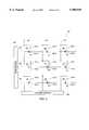
- FIG. 1is a schematic diagram of a PROM cell according to the present invention.
- FIG. 2is a top view of the layout of a group of four PROM cells fabricated on a p-type substrate with an N-Channel select transistor and an antifuse as the programming element.
- FIG. 3is a cross sectional view of a single one of the PROM cells of the view of FIG. 2, taken through the center of one of the metal lines.
- FIG. 4is a schematic diagram of an illustrative PROM array according to the present invention.
- PROM cell 10comprises an antifuse 12 connected between a bit line 14 and the drain of an N-Channel MOS select transistor 16.
- the gate of the N-Channel MOS select transistor 16is connected to a word line 18 and the source of the N-Channel MOS select transistor 16 is connected to ground.
- the N-Channel select transistormay be formed at the minimum feature size for the fabrication technology employed.
- the antifuseis of the type disclosed in U.S. Pat. No. 4,823,181 to Mohsen et al., and in U.S. Pat. No. 4,899,205 to Hamdy et al.
- the lower electrode of the antifuse 12is formed from a diffused region in a p-type semiconductor substrate, preferably a P+epi substrate as is known in the art.
- the lower antifuse electrodeis formed from a lightly doped phosphorus region.
- the lower electrode of the antifuseis formed from a phosphorus diffusion doped to a concentration of between about 1e17 and about 1e19.
- An antifuse layerpreferably comprising an oxide, oxide-nitride, or oxide-nitride-oxide antifuse layer, as known in the prior art, is formed over the lower antifuse electrode, and an upper antifuse electrode is formed from heavily doped polysilicon preferably as taught by Hamdy et al. in U.S. Pat. No. 4,899,205.
- FIG. 2a top view is presented of the layout of a group of four PROM cells 10a, 10b, 10c, and 10d fabricated on a grounded p-type substrate comprising a P+ region 20a and an epitaxial P- region 20b.
- Each cellemploys an antifuse as the programming element with an N-Channel select transistor.
- FIG. 3is a cross sectional view through the substrate at the center of a pair of the PROM cells of the present invention. Viewing FIGS. 2 and 3 together will facilitate an understanding of the present invention.
- FIG. 2Reference is made to cell 10a in the upper left-hand comer of FIG. 2 for a disclosure of the PROM cell of the present invention.
- Cells 10b, 10c, and 10dare virtually identical mirror images of cell 10a.
- Elements in each of the PROM cells in FIG. 2will be given the alphabetical suffix corresponding to the alphabetical suffix of their cell's reference numeral.
- FIG. 3will be assumed to depict all of PROM cell 10a and a portion of PROM cell 10b, as well as a portion of an unidentified cell at the right hand side of the figure.
- elements of FIG. 1 which appear thereinwill be given the same reference numerals as in FIG. 1, followed of course by the appropriate alphabetical suffix.
- Bit line 14 of FIG. 1is a metal line running vertically in FIG. 2 on both the left and right portions of the figure.
- the metal line at the left portion of FIG. 2is bit line 14a in the top half of the figure and bit line 14b in the bottom half of the figure.
- the metal line at the right portion of FIG. 2is bit line 14c in the top half of the figure and bit line 14d in the bottom half of the figure.
- Word line 18 of FIG. 1is a polysilicon line running horizontally in FIG. 2 on both the top and bottom portions of the figure.
- the polysilicon line at the top portion of FIG. 2is bit line 18a in the left half of the figure and bit line 18c in the right half of the figure.
- the polysilicon line at the bottom portion of FIG. 2is bit line 18b in the left half of the figure and bit line 18d in the right half of the figure.
- PROM cell 10a in FIG. 3starts on the left at diffused region 22a and 22b which forms the source diffusion for the N-Channel select transistor of PROM cell 10a as well as the source of the N-Channel select transistor of PROM cell 10b mirrored to the left.
- PROM cell 10aends on the right at the center of field oxide region 24. Everything to the right of the center of field oxide region 24 is a portion of another PROM cell mirrored to the right.
- N- region 28acomprises a phosphorus doped region at a concentration of between about 1e17 and about 1e19, and forms the lower antifuse electrode.
- the surrounding N+ region 26acomprises an arsenic doped region at a concentration of between about 1e19 and about 1e21, preferably about 1e20, and forms the drain of N-Channel MOS select transistor 16 of FIG. 1. The fact that regions 26a and 28a are contiguous assures connection between the lower antifuse electrode and the drain of the select transistor.
- an oxide layer 30ais disposed over diffused regions 26a and 28a.
- Antifuse layer 32ais disposed in an aperture formed in the oxide layer 30a in alignment with diffused region 28a.
- antifuse layer 32acomprises about 35 angstroms of thermal silicon dioxide, about 65 angstroms of deposited silicon nitride, and about 25 angstroms of thermal silicon dioxide converted from the layer of silicon nitride.
- the left half of a polysilicon layer identified by reference numeral 34aforms the upper electrode of antifuse 12a.
- the right half of that same polysilicon layer 34xforms the upper electrode of an antifuse 12x in a neighboring cell.
- Metal line 14aconnects to polysilicon layer 34a at contact region 36.
- a channel 38a for the select transistoris bounded on its left by diffused region 22a, the source of the N-Channel MOS select transistor 16a.
- Diffused region 22b, the left half of the same diffusion,begins PROM cell 10b as the source of the N-Channel MOS select transistor 16b. This diffusion is connected to ground.
- a gate oxide region 40a overlying channel region 38aseparates channel region 38a from the polysilicon word line 18a,c of FIG. 2 and a gate oxide region 40b overlying channel region 38b, separates channel region 38b from the polysilicon word line 18b,d of FIG. 2.
- the rightmost polysilicon stripis the portion 18a of polysilicon word line 18a,c of FIG. 2 which forms the gate of N-Channel MOS select transistor 16a
- the leftmost polysilicon stripis the portion 18b of the polysilicon word line 18b,d which forms the gate of N-Channel MOS select transistor 16a.
- Another portion of oxide layer 30ais shown in FIG. 3 disposed above polysilicon gates 18a and 18b.
- PROM cells 10b, 10c, and 10dwould be apparent from the above disclosure of PROM cell 10a.
- the PROM cell of the present inventionmay be fabricated as a part of a conventional CMOS semiconductor fabrication process.
- the processpreferably starts with a P+ substrate including a P- epitaxial layer formed thereon.
- Conventional front end stepsare performed to create field oxide channel stop regions for all active devices to be formed on the substrate.
- Field oxide region 24 of FIG. 3is created at this time.
- the transistor devicesare formed using self-aligned gate techniques, a gate oxide layer is formed and a polysilicon layer is deposited thereover, doped, and defined to form the word lines and select transistor gates.
- the N+ and N- regions for the antifuse and select transistorsare formed using conventional CMOS implant techniques.
- the step for formation of the N- region for the lower antifuse electrodemay already be present in a CMOS process for formation of lightly-doped drain (LDD) regions for other transistors.
- the lower antifuse electrodemay be formed simply by including the additional apertures in the LDD mask already used in the process. Otherwise a second implant step will be inserted into the process to form the N- lower antifuse electrode diffusion.
- an oxide layeris formed to cover the word line polysilicon and form the interlayer dielectric for the antifuses.
- Masking and etching stepsare then performed to form the antifuse apertures and the antifuse dielectrics are formed in the apertures.
- Conventional semiconductor processing techniquesare then used to form another insulating layer through which contact apertures (including the contact for the metal to cell polysilicon connection) are etched as is known in the art.
- a metal interconnect layeris deposited and defined over that layer to form the metal bit line.
- Conventional rear-end stepsare then performed to complete the semiconductor structure.
- the antifuse layer 32awill break down and the local temperature of the N-diffused region 28a will exceed the melting point of the silicon. A large quantity of holes and electrons will be generated in this process. The electrons will flow to the top plate and the holes will flow into the N- diffused region 28a.
- N- region 28ais doped lightly, the probability of the holes recombining is very small. Thus, the holes flow straight to the grounded P+ substrate 20 as shown in FIG. 3 by arrows 42. To maintain this current flow a voltage of at least 2.5 volts must be maintained across the antifuse dielectric. The N-diffused region 28a must therefore receive a supply of electrons from ground.
- N-Channel select transistor 16aThese electrons are initially supplied by the N-Channel select transistor 16a. If the demand for this current is exceeded, the localized substrate potential will be raised by the injected holes thus forward biasing the source of the N-Channel select transistor 16a. This condition will supply any excess electrons required. Those of ordinary skill in the art will appreciate that, under these conditions, any amount of programming current can be achieved.
- the SCR action of the antifuse structure depicted in FIGS. 2 and 3relies on a "virtual" P+ region at the top of the N- region 28a caused by the melting silicon material during the programming process.
- the hot spot in the silicon generated by the breakdown of the dielectric during programmingis a source of holes just as a P+ region would be in normal semiconductor operation. Since the programming process generates temperatures in excess of the melting point of the silicon in region 28a, holes and electrons are produced in large numbers. The electrons are attracted to the positive programming potential at the metal bit line 14a and the holes will be attracted to the grounded P+ substrate 20a just as holes from a P+ region would be so attracted.
- This virtual P+ regionis forward biased with respect to the N- region 28a, which thus injects a large number of holes into the P- epi region 22b of the substrate, thus forward biasing that region with respect to N+ region 22a, the source of the select transistor 16, thus injecting many electrons back into P- region 22b and sustaining the forward biasing of the "virtual" P+ region in N- region 28a.
- Thisis the common four-layer structure for SCR action, even though one of the layers is a virtual layer.
- the sustaining voltage for the hot spotwill be a bias of at least about 2.5 to 3 volts across the dielectric to keep the temperature high. This phenomenon allows substrate hole injection only during programming.
- the injected substrate currentwill discharge the adjacent antifuse substrate nodes to ground and will result in applying the voltage on the bit line 14a across whatever other unprogrammed antifuses in the array containing PROM cell 10a are connected to that bit line 14a. This not a problem because the impedance of the devices supplying the bit lines with programming current will clamp the voltage on the bit line to a value below that of the programming voltage of the antifuse dielectric at the instant the selected antifuse is blown.
- the current through the antifuse connectionis low enough to avoid heating up the silicon enough to cause it to create the "virtual" P+ region and go into SCR latchup.
- the only remaining issueis the fact that the lightly doped N- region 28a does have a significant spreading resistance. This can be tailored somewhat by increasing the doping as much as possible without stopping the SCR action. This limit is presently believed to be about 1e19. In many applications this is not very important though as electrons injected into the N- region 28a by the surrounding N+ region 26a will lower the resistance of the N- region 28a. This will create a slight nonlinearity in the resistance of the device of only about 0.3V. This can easily be accounted for in the design of the circuit by setting the trip point of the sense amplifier somewhat higher, i.e., about 0.5 volt.
- FIG. 4is a schematic diagram of the core of an illustrative PROM array 50 according to this aspect of the present invention. While PROM array 50 is shown as a 3 by 3 array, persons of ordinary skill in the art will observe that it is merely illustrative and that PROM arrays of arbitrary size are possible using the technology of the present invention.
- Bit line 52is associated with a first column of array 50.
- bit lines 54 and 56are associated with second and third columns of array 50.
- word line 58is associated with a first row of array 50.
- word lines 60 and 62are associated with second and third rows of array 50.
- Array 50includes nine PROM cells.
- PROM cells 64, 66, and 68comprise the first row of the array;
- PROM cells 70, 72, and 74comprise the second row of the array;
- PROM cells 76, 78, and 80comprise the third row of the array.
- PROM cells 64, 70, and 76comprise the first column of the array;
- PROM cells 66, 72, and 78comprise the second column of the array;
- PROM cells 68, 74, and 80comprise the third column of the array.
- bit line 52is connected to the lower electrodes of antifuses 64-1, 70-1, and 76-1 bit line 54 is connected to the lower electrodes of antifuses 66-1, 72-1, and 78-1, bit line 56 is connected to the lower electrodes of antifuses 68-1, 74-1, and 80-1.
- each word lineis connected to the upper antifuse electrode of the antifuse in all of the cells in its row.
- Word line 58is connected to the upper electrodes of antifuses 64-1, 66-1, and 68-1
- Word line 60is connected to the upper electrodes of antifuses 60-1, 72-1, and 74-1
- Word line 62is connected to the upper electrodes of antifuses 76-1, 78-1, and 80-1.
- bit lines 52, 54, and 56are driven by column decoder/driver 82 and word lines 58, 60, and 62 are driven by row decoder/driver 84. Address decoding is well understood in the art.
- bit line and word line associated with that cellare asserted in programming mode with programming mode voltages, causing the appropriate antifuse to program as taught herein.
- programming mode voltagesare asserted on bit line 54 and word line 60.
- bit line and word line associated with that cellare asserted in read mode with read mode voltages, causing the appropriate antifuse to be read as taught herein.
- read mode voltagesare asserted on bit line 54 and word line 60.
Landscapes
- Semiconductor Memories (AREA)
- Read Only Memory (AREA)
Abstract
Description
Claims (11)
Priority Applications (3)
| Application Number | Priority Date | Filing Date | Title |
|---|---|---|---|
| US08/797,202US5909049A (en) | 1997-02-11 | 1997-02-11 | Antifuse programmed PROM cell |
| PCT/US1998/002924WO1998035387A1 (en) | 1997-02-11 | 1998-02-10 | Antifuse programmed prom cell |
| EP98905091AEP0976158A4 (en) | 1997-02-11 | 1998-02-10 | Antifuse programmed prom cell |
Applications Claiming Priority (1)
| Application Number | Priority Date | Filing Date | Title |
|---|---|---|---|
| US08/797,202US5909049A (en) | 1997-02-11 | 1997-02-11 | Antifuse programmed PROM cell |
Publications (1)
| Publication Number | Publication Date |
|---|---|
| US5909049Atrue US5909049A (en) | 1999-06-01 |
Family
ID=25170196
Family Applications (1)
| Application Number | Title | Priority Date | Filing Date |
|---|---|---|---|
| US08/797,202Expired - LifetimeUS5909049A (en) | 1997-02-11 | 1997-02-11 | Antifuse programmed PROM cell |
Country Status (3)
| Country | Link |
|---|---|
| US (1) | US5909049A (en) |
| EP (1) | EP0976158A4 (en) |
| WO (1) | WO1998035387A1 (en) |
Cited By (48)
| Publication number | Priority date | Publication date | Assignee | Title |
|---|---|---|---|---|
| US6515931B2 (en)* | 1996-08-20 | 2003-02-04 | Micron Technology, Inc. | Method of anti-fuse repair |
| US20030063518A1 (en)* | 2001-09-18 | 2003-04-03 | David Fong | Programming methods and circuits for semiconductor memory cell and memory array using a breakdown phenomena in an ultra-thin dielectric |
| US20030071315A1 (en)* | 2001-10-17 | 2003-04-17 | Jack Zezhong Peng | Reprogrammable non-volatile memory using a breakdown phenomena in an ultra-thin dielectric |
| US20030115518A1 (en)* | 2001-12-14 | 2003-06-19 | Bendik Kleveland | Memory device and method for redundancy/self-repair |
| US20030178033A1 (en)* | 1996-02-19 | 2003-09-25 | Cosgrove Delos M. | Minimally invasive cardiac surgery procedure |
| US20030198085A1 (en)* | 2001-09-18 | 2003-10-23 | Peng Jack Zezhong | Semiconductor memory cell and memory array using a breakdown phenomena in an ultra-thin dielectric |
| US20030202376A1 (en)* | 2002-04-26 | 2003-10-30 | Peng Jack Zezhong | High density semiconductor memory cell and memory array using a single transistor |
| US6650143B1 (en) | 2002-07-08 | 2003-11-18 | Kilopass Technologies, Inc. | Field programmable gate array based upon transistor gate oxide breakdown |
| US20040004269A1 (en)* | 2002-07-08 | 2004-01-08 | International Business Machines Corporation | High impedance antifuse |
| US20040031853A1 (en)* | 2001-10-17 | 2004-02-19 | Peng Jack Zezhong | Smart card having memory using a breakdown phenomena in an ultra-thin dielectric |
| US20040125671A1 (en)* | 2002-04-26 | 2004-07-01 | Peng Jack Zezhong | High density semiconductor memory cell and memory array using a single transistor having a buried N+ connection |
| US20040156234A1 (en)* | 2002-04-26 | 2004-08-12 | Peng Jack Zezhong | High density semiconductor memory cell and memory array using a single transistor and having variable gate oxide breakdown |
| US6791891B1 (en) | 2003-04-02 | 2004-09-14 | Kilopass Technologies, Inc. | Method of testing the thin oxide of a semiconductor memory cell that uses breakdown voltage |
| US20040190357A1 (en)* | 2003-03-28 | 2004-09-30 | Scheuerlein Roy E. | Redundant memory structure using bad bit pointers |
| US20040208055A1 (en)* | 2002-09-26 | 2004-10-21 | Jianguo Wang | Methods and circuits for testing programmability of a semiconductor memory cell and memory array using a breakdown phenomenon in an ultra-thin dielectric |
| US20040223370A1 (en)* | 2002-09-26 | 2004-11-11 | Jianguo Wang | Methods and circuits for programming of a semiconductor memory cell and memory array using a breakdown phenomenon in an ultra-thin dielectric |
| US20040223363A1 (en)* | 2002-04-26 | 2004-11-11 | Peng Jack Zezhong | High density semiconductor memory cell and memory array using a single transistor and having counter-doped poly and buried diffusion wordline |
| US6836000B1 (en) | 2000-03-01 | 2004-12-28 | Micron Technology, Inc. | Antifuse structure and method of use |
| US20050026336A1 (en)* | 2002-08-29 | 2005-02-03 | Porter Stephen R. | Current limiting antifuse programming path |
| US20050035783A1 (en)* | 2003-08-15 | 2005-02-17 | Man Wang | Field programmable gate array |
| US20050169040A1 (en)* | 2004-02-03 | 2005-08-04 | Peng Jack Z. | Combination field programmable gate array allowing dynamic reprogrammability |
| US20050169039A1 (en)* | 2004-02-03 | 2005-08-04 | Peng Jack Z. | Combination field programmable gate array allowing dynamic reprogrammability and non-volatile programmability based upon transistor gate oxide breakdown |
| US20050218929A1 (en)* | 2004-04-02 | 2005-10-06 | Man Wang | Field programmable gate array logic cell and its derivatives |
| US20050258482A1 (en)* | 2002-07-18 | 2005-11-24 | Broadcom Corporation | Anti-fuse device |
| US20050275428A1 (en)* | 2004-06-10 | 2005-12-15 | Guy Schlacter | Field programmable gate array logic unit and its cluster |
| US20050275427A1 (en)* | 2004-06-10 | 2005-12-15 | Man Wang | Field programmable gate array logic unit and its cluster |
| US20060062068A1 (en)* | 2004-09-20 | 2006-03-23 | Guy Schlacter | Field programmable gate arrays using both volatile and nonvolatile memory cell properties and their control |
| US20060067152A1 (en)* | 2004-09-29 | 2006-03-30 | Ali Keshavarzi | Crosspoint memory array utilizing one time programmable antifuse cells |
| US20060071646A1 (en)* | 2004-09-30 | 2006-04-06 | Fabrice Paillet | Non volatile data storage through dielectric breakdown |
| US20060140026A1 (en)* | 2004-12-28 | 2006-06-29 | Alper Ilkbahar | Method and apparatus for improving yield in semiconductor devices by guaranteeing health of redundancy information |
| US20060176636A1 (en)* | 2005-02-07 | 2006-08-10 | Samsung Electronics Co., Ltd. | Electrical fuse circuits and methods of forming the same |
| US20060232296A1 (en)* | 2005-04-18 | 2006-10-19 | Kilopass Technologies, Inc. | Fast processing path using field programmable gate array logic unit |
| US20060291303A1 (en)* | 2005-06-22 | 2006-12-28 | Bendik Kleveland | Method and apparatus for programming a memory array |
| US20070114596A1 (en)* | 2005-11-21 | 2007-05-24 | Stmicroelectronics S.A. | Integrated electronic circuit incorporating a capacitor |
| US20070279086A1 (en)* | 2006-06-01 | 2007-12-06 | Wilcox William J | Antifuse programming circuit with snapback select transistor |
| US20080246098A1 (en)* | 2004-05-06 | 2008-10-09 | Sidense Corp. | Split-channel antifuse array architecture |
| US20080285365A1 (en)* | 2007-05-15 | 2008-11-20 | Bosch Derek J | Memory device for repairing a neighborhood of rows in a memory array using a patch table |
| US20080288813A1 (en)* | 2007-05-15 | 2008-11-20 | Bosch Derek J | Method for repairing a neighborhood of rows in a memory array using a patch table |
| US20090262566A1 (en)* | 2006-12-22 | 2009-10-22 | Sidense Corp. | Mask programmable anti-fuse architecture |
| US20090315109A1 (en)* | 2008-06-20 | 2009-12-24 | Kim Min-Seok | Semiconductor device having otp cells and method for fabricating the same |
| US20100244115A1 (en)* | 2004-05-06 | 2010-09-30 | Sidense Corporation | Anti-fuse memory cell |
| CN103035647A (en)* | 2011-10-04 | 2013-04-10 | 美国博通公司 | One-time programmable device having an LDMOS structure and related method |
| US8669806B2 (en) | 2012-03-05 | 2014-03-11 | Robert Newton Rountree | Low voltage antifuse programming circuit and method |
| US20140071779A1 (en)* | 2012-09-11 | 2014-03-13 | Sungju SON | E-fuse array circuit |
| US8735297B2 (en) | 2004-05-06 | 2014-05-27 | Sidense Corporation | Reverse optical proximity correction method |
| US8842488B2 (en) | 2012-02-08 | 2014-09-23 | Robert Newton Rountree | Low voltage efuse programming circuit and method |
| US9123572B2 (en) | 2004-05-06 | 2015-09-01 | Sidense Corporation | Anti-fuse memory cell |
| US10127993B2 (en) | 2015-07-29 | 2018-11-13 | National Chiao Tung University | Dielectric fuse memory circuit and operation method thereof |
Families Citing this family (1)
| Publication number | Priority date | Publication date | Assignee | Title |
|---|---|---|---|---|
| WO2002043152A2 (en) | 2000-11-27 | 2002-05-30 | Koninklijke Philips Electronics N.V. | Poly fuse rom |
Citations (168)
| Publication number | Priority date | Publication date | Assignee | Title |
|---|---|---|---|---|
| US3191151A (en)* | 1962-11-26 | 1965-06-22 | Fairchild Camera Instr Co | Programmable circuit |
| US3204127A (en)* | 1963-07-12 | 1965-08-31 | Collins Radio Co | Digit memory circuit |
| US3431433A (en)* | 1964-05-29 | 1969-03-04 | Robert George Ball | Digital storage devices using field effect transistor bistable circuits |
| US3576549A (en)* | 1969-04-14 | 1971-04-27 | Cogar Corp | Semiconductor device, method, and memory array |
| US3582908A (en)* | 1969-03-10 | 1971-06-01 | Bell Telephone Labor Inc | Writing a read-only memory while protecting nonselected elements |
| US3641516A (en)* | 1969-09-15 | 1972-02-08 | Ibm | Write once read only store semiconductor memory |
| US3668655A (en)* | 1970-03-26 | 1972-06-06 | Cogar Corp | Write once/read only semiconductor memory array |
| US3699543A (en)* | 1968-11-04 | 1972-10-17 | Energy Conversion Devices Inc | Combination film deposited switch unit and integrated circuits |
| US3699403A (en)* | 1970-10-23 | 1972-10-17 | Rca Corp | Fusible semiconductor device including means for reducing the required fusing current |
| US3699395A (en)* | 1970-01-02 | 1972-10-17 | Rca Corp | Semiconductor devices including fusible elements |
| US3717852A (en)* | 1971-09-17 | 1973-02-20 | Ibm | Electronically rewritable read-only memory using via connections |
| US3733690A (en)* | 1970-07-13 | 1973-05-22 | Intersil Inc | Double junction read only memory and process of manufacture |
| US3742592A (en)* | 1970-07-13 | 1973-07-03 | Intersil Inc | Electrically alterable integrated circuit read only memory unit and process of manufacturing |
| US3750115A (en)* | 1972-04-28 | 1973-07-31 | Gen Electric | Read mostly associative memory cell for universal logic |
| US3781977A (en)* | 1970-09-19 | 1974-01-01 | Ferrant Ltd | Semiconductor devices |
| US3792319A (en)* | 1972-01-19 | 1974-02-12 | Intel Corp | Poly-crystalline silicon fusible links for programmable read-only memories |
| US3848238A (en)* | 1970-07-13 | 1974-11-12 | Intersil Inc | Double junction read only memory |
| US3967251A (en)* | 1975-04-17 | 1976-06-29 | Xerox Corporation | User variable computer memory module |
| FR2367352A1 (en) | 1976-10-08 | 1978-05-05 | Westinghouse Electric Corp | DIGITAL MEMORY |
| US4099260A (en)* | 1976-09-20 | 1978-07-04 | Bell Telephone Laboratories, Incorporated | Bipolar read-only-memory unit having self-isolating bit-lines |
| US4125880A (en)* | 1977-03-09 | 1978-11-14 | Harris Corporation | Simplified output circuit for read only memories |
| US4127900A (en)* | 1976-10-29 | 1978-11-28 | Massachusetts Institute Of Technology | Reading capacitor memories with a variable voltage ramp |
| US4146902A (en)* | 1975-12-03 | 1979-03-27 | Nippon Telegraph And Telephone Public Corp. | Irreversible semiconductor switching element and semiconductor memory device utilizing the same |
| US4174521A (en)* | 1978-04-06 | 1979-11-13 | Harris Corporation | PROM electrically written by solid phase epitaxy |
| US4177475A (en)* | 1977-10-31 | 1979-12-04 | Burroughs Corporation | High temperature amorphous memory device for an electrically alterable read-only memory |
| US4203123A (en)* | 1977-12-12 | 1980-05-13 | Burroughs Corporation | Thin film memory device employing amorphous semiconductor materials |
| US4208727A (en)* | 1978-06-15 | 1980-06-17 | Texas Instruments Incorporated | Semiconductor read only memory using MOS diodes |
| US4209894A (en)* | 1978-04-27 | 1980-07-01 | Texas Instruments Incorporated | Fusible-link semiconductor memory |
| US4238839A (en)* | 1979-04-19 | 1980-12-09 | National Semiconductor Corporation | Laser programmable read only memory |
| US4253059A (en)* | 1979-05-14 | 1981-02-24 | Fairchild Camera & Instrument Corp. | EPROM Reliability test circuit |
| US4257832A (en)* | 1978-07-24 | 1981-03-24 | Siemens Aktiengesellschaft | Process for producing an integrated multi-layer insulator memory cell |
| US4281398A (en)* | 1980-02-12 | 1981-07-28 | Mostek Corporation | Block redundancy for memory array |
| US4322822A (en)* | 1979-01-02 | 1982-03-30 | Mcpherson Roger K | High density VMOS electrically programmable ROM |
| US4323986A (en)* | 1980-06-30 | 1982-04-06 | International Business Machines Corporation | Electronic storage array having DC stable conductivity modulated storage cells |
| US4347586A (en)* | 1979-06-07 | 1982-08-31 | Nippon Electric Co., Ltd. | Semiconductor memory device |
| US4399450A (en)* | 1977-11-28 | 1983-08-16 | U.S. Philips Corporation | ROM With poly-Si to mono-Si diodes |
| US4404581A (en)* | 1980-12-15 | 1983-09-13 | Rockwell International Corporation | ROM With redundant ROM cells employing a highly resistive polysilicon film for programming the cells |
| EP0089457A2 (en) | 1982-03-23 | 1983-09-28 | Texas Instruments Incorporated | Avalanche fuse element as programmable memory |
| US4418403A (en)* | 1981-02-02 | 1983-11-29 | Mostek Corporation | Semiconductor memory cell margin test circuit |
| US4420820A (en)* | 1980-12-29 | 1983-12-13 | Signetics Corporation | Programmable read-only memory |
| US4420504A (en)* | 1980-12-22 | 1983-12-13 | Raytheon Company | Programmable read only memory |
| US4424579A (en)* | 1981-02-23 | 1984-01-03 | Burroughs Corporation | Mask programmable read-only memory stacked above a semiconductor substrate |
| US4424578A (en)* | 1980-07-14 | 1984-01-03 | Tokyo Shibaura Denki Kabushiki Kaisha | Bipolar prom |
| FR2530383A1 (en) | 1982-07-13 | 1984-01-20 | Thomson Csf | MONOLITHIC INTEGRATED CIRCUIT COMPRISING A SCHOTTKY LOGIC PART AND A PROGRAMMABLE FUSE MEMORY |
| US4441167A (en)* | 1981-12-03 | 1984-04-03 | Raytheon Company | Reprogrammable read only memory |
| US4442507A (en)* | 1981-02-23 | 1984-04-10 | Burroughs Corporation | Electrically programmable read-only memory stacked above a semiconductor substrate |
| EP0041770A3 (en) | 1980-05-23 | 1984-07-11 | Texas Instruments Incorporated | A programmable read-only-memory element and method of fabrication thereof |
| US4488262A (en)* | 1981-06-25 | 1984-12-11 | International Business Machines Corporation | Electronically programmable read only memory |
| US4494135A (en)* | 1976-04-06 | 1985-01-15 | U.S. Philips Corporation | Programmable read only memory cell having an electrically destructible programmation element integrally formed with a junction diode |
| US4499557A (en)* | 1980-10-28 | 1985-02-12 | Energy Conversion Devices, Inc. | Programmable cell for use in programmable electronic arrays |
| US4502208A (en)* | 1979-01-02 | 1985-03-05 | Texas Instruments Incorporated | Method of making high density VMOS electrically-programmable ROM |
| US4507757A (en)* | 1982-03-23 | 1985-03-26 | Texas Instruments Incorporated | Avalanche fuse element in programmable memory |
| US4507673A (en)* | 1979-10-13 | 1985-03-26 | Tokyo Shibaura Denki Kabushiki Kaisha | Semiconductor memory device |
| EP0053878B1 (en) | 1980-12-08 | 1985-08-14 | Kabushiki Kaisha Toshiba | Semiconductor memory device |
| US4553225A (en)* | 1981-09-26 | 1985-11-12 | Fujitsu Limited | Method of testing IC memories |
| US4565712A (en)* | 1980-04-24 | 1986-01-21 | Tokyo Shibaura Denki Kabushiki Kaisha | Method of making a semiconductor read only memory |
| US4565932A (en)* | 1983-12-29 | 1986-01-21 | Motorola, Inc. | High voltage circuit for use in programming memory circuits (EEPROMs) |
| US4569120A (en)* | 1983-03-07 | 1986-02-11 | Signetics Corporation | Method of fabricating a programmable read-only memory cell incorporating an antifuse utilizing ion implantation |
| US4569121A (en)* | 1983-03-07 | 1986-02-11 | Signetics Corporation | Method of fabricating a programmable read-only memory cell incorporating an antifuse utilizing deposition of amorphous semiconductor layer |
| US4590589A (en)* | 1982-12-21 | 1986-05-20 | Zoran Corporation | Electrically programmable read only memory |
| US4595875A (en)* | 1983-12-22 | 1986-06-17 | Monolithic Memories, Incorporated | Short detector for PROMS |
| US4597062A (en)* | 1981-03-03 | 1986-06-24 | Tokyo Shibaura Denki Kabushiki Kaisha | Non-volatile semiconductor memory system |
| US4598386A (en)* | 1984-04-18 | 1986-07-01 | Roesner Bruce B | Reduced-area, read-only memory |
| US4599705A (en)* | 1979-12-13 | 1986-07-08 | Energy Conversion Devices, Inc. | Programmable cell for use in programmable electronic arrays |
| US4601034A (en)* | 1984-03-30 | 1986-07-15 | Texas Instruments Incorporated | Method and apparatus for testing very large scale integrated memory circuits |
| US4612630A (en)* | 1984-07-27 | 1986-09-16 | Harris Corporation | EEPROM margin testing design |
| US4613886A (en)* | 1981-07-09 | 1986-09-23 | Intel Corporation | CMOS static memory cell |
| US4646264A (en)* | 1982-06-28 | 1987-02-24 | Fujitsu Limited | Programmable read-only memory device |
| US4647340A (en)* | 1986-03-31 | 1987-03-03 | Ncr Corporation | Programmable read only memory using a tungsten fuse |
| US4651304A (en)* | 1982-12-09 | 1987-03-17 | Ricoh Company, Ltd. | EPROM memory device having a test circuit |
| US4653029A (en)* | 1984-04-06 | 1987-03-24 | Hitachi, Ltd. | MOS amplifier and semiconductor memory using the same |
| US4658380A (en)* | 1986-02-28 | 1987-04-14 | Ncr Corporation | CMOS memory margining control circuit for a nonvolatile memory |
| US4692787A (en)* | 1980-05-23 | 1987-09-08 | Texas Instruments Incorporated | Programmable read-only-memory element with polycrystalline silicon layer |
| US4698589A (en)* | 1986-03-21 | 1987-10-06 | Harris Corporation | Test circuitry for testing fuse link programmable memory devices |
| US4725985A (en)* | 1983-11-09 | 1988-02-16 | Kabushiki Kaisha Toshiba | Circuit for applying a voltage to a memory cell MOS capacitor of a semiconductor memory device |
| US4742492A (en)* | 1985-09-27 | 1988-05-03 | Texas Instruments Incorporated | EEPROM memory cell having improved breakdown characteristics and driving circuitry therefor |
| US4748490A (en)* | 1985-08-01 | 1988-05-31 | Texas Instruments Incorporated | Deep polysilicon emitter antifuse memory cell |
| US4750155A (en)* | 1985-09-19 | 1988-06-07 | Xilinx, Incorporated | 5-Transistor memory cell which can be reliably read and written |
| US4782487A (en)* | 1987-05-15 | 1988-11-01 | Digital Equipment Corporation | Memory test method and apparatus |
| US4782466A (en)* | 1985-09-04 | 1988-11-01 | Fujitsu Limited | Programmable semiconductor read only memory device |
| US4792835A (en)* | 1986-12-05 | 1988-12-20 | Texas Instruments Incorporated | MOS programmable memories using a metal fuse link and process for making the same |
| US4796074A (en)* | 1987-04-27 | 1989-01-03 | Instant Circuit Corporation | Method of fabricating a high density masked programmable read-only memory |
| EP0162529B1 (en) | 1984-01-13 | 1989-03-01 | The British Petroleum Company p.l.c. | Amorphous or microcrystalline semiconductor memory device |
| US4821233A (en)* | 1985-09-19 | 1989-04-11 | Xilinx, Incorporated | 5-transistor memory cell with known state on power-up |
| US4822750A (en)* | 1983-08-29 | 1989-04-18 | Seeq Technology, Inc. | MOS floating gate memory cell containing tunneling diffusion region in contact with drain and extending under edges of field oxide |
| EP0172193B1 (en) | 1984-02-09 | 1989-04-19 | Ncr Corporation | Programmable read-only memory cell and method of fabrication |
| US4839864A (en)* | 1987-03-09 | 1989-06-13 | Mitsubishi Denki Kabushiki Kaisha | Semiconductor memory device comprising programmable redundancy circuit |
| US4851364A (en)* | 1979-05-25 | 1989-07-25 | Hitachi, Ltd. | Method of forming well regions for field effect transistors utilizing self-aligned techniques |
| US4851361A (en)* | 1988-02-04 | 1989-07-25 | Atmel Corporation | Fabrication process for EEPROMS with high voltage transistors |
| US4876220A (en)* | 1986-05-16 | 1989-10-24 | Actel Corporation | Method of making programmable low impedance interconnect diode element |
| US4878199A (en)* | 1987-02-27 | 1989-10-31 | Kabushiki Kaisha Toshiba | Semiconductor memory device |
| US4881114A (en)* | 1986-05-16 | 1989-11-14 | Actel Corporation | Selectively formable vertical diode circuit element |
| US4899205A (en)* | 1986-05-09 | 1990-02-06 | Actel Corporation | Electrically-programmable low-impedance anti-fuse element |
| US4901128A (en)* | 1982-11-04 | 1990-02-13 | Hitachi, Ltd. | Semiconductor memory |
| US4903266A (en)* | 1988-04-29 | 1990-02-20 | International Business Machines Corporation | Memory self-test |
| DE3927033A1 (en) | 1988-08-23 | 1990-03-01 | Seiko Epson Corp | SEMICONDUCTOR ELEMENT AND METHOD FOR THE PRODUCTION THEREOF |
| US4908799A (en)* | 1986-06-24 | 1990-03-13 | Thomson Composants Militaires Et Spatiaux | Device to detect the functioning of the read system of an EPROM or EEPROM memory cell |
| US4933735A (en)* | 1981-02-23 | 1990-06-12 | Unisys Corporation | Digital computer having control and arithmetic sections stacked above semiconductor substrate |
| US4958324A (en)* | 1987-11-24 | 1990-09-18 | Sgs-Thomson Microelectronics Sa | Method for the testing of electrically programmable memory cells, and corresponding integrated circuit |
| US4963825A (en)* | 1989-12-21 | 1990-10-16 | Intel Corporation | Method of screening EPROM-related devices for endurance failure |
| US5015885A (en)* | 1986-09-19 | 1991-05-14 | Actel Corporation | Reconfigurable programmable interconnect architecture |
| US5027320A (en)* | 1989-09-22 | 1991-06-25 | Cypress Semiconductor Corp. | EPROM circuit having enhanced programmability and improved speed and reliability |
| US5056089A (en)* | 1988-02-08 | 1991-10-08 | Mitsubishi Denki Kabushiki Kaisha | Memory device |
| US5075249A (en)* | 1988-04-04 | 1991-12-24 | Fujitsu Limited | Method of making a bic memory cell having contact openings with straight sidewalls and sharp-edge rims |
| US5079746A (en)* | 1988-02-08 | 1992-01-07 | Fujitsu Limited | Semiconductor memory circuit |
| US5086008A (en)* | 1988-02-29 | 1992-02-04 | Sgs-Thomson Microelectronics S.R.L. | Process for obtaining high-voltage N channel transistors particularly for EEPROM memories with CMOS technology |
| US5086331A (en)* | 1988-04-05 | 1992-02-04 | U.S. Philips Corp. | Integrated circuit comprising a programmable cell |
| US5091908A (en)* | 1990-02-06 | 1992-02-25 | At&T Bell Laboratories | Built-in self-test technique for read-only memories |
| US5093711A (en) | 1988-10-14 | 1992-03-03 | Seiko Epson Corporation | Semiconductor device |
| US5101409A (en) | 1989-10-06 | 1992-03-31 | International Business Machines Corporation | Checkboard memory self-test |
| US5107501A (en) | 1990-04-02 | 1992-04-21 | At&T Bell Laboratories | Built-in self-test technique for content-addressable memories |
| US5113238A (en) | 1989-01-06 | 1992-05-12 | Wang Chen Chin | Contactless non-volatile memory array cells |
| US5126290A (en) | 1991-09-11 | 1992-06-30 | Micron Technology, Inc. | Method of making memory devices utilizing one-sided ozone teos spacers |
| US5134584A (en) | 1988-07-22 | 1992-07-28 | Vtc Incorporated | Reconfigurable memory |
| US5138619A (en) | 1990-02-15 | 1992-08-11 | National Semiconductor Corporation | Built-in self test for integrated circuit memory |
| US5163180A (en) | 1991-01-18 | 1992-11-10 | Actel Corporation | Low voltage programming antifuse and transistor breakdown method for making same |
| US5166901A (en) | 1986-05-14 | 1992-11-24 | Raytheon Company | Programmable memory cell structure including a refractory metal barrier layer |
| US5191550A (en) | 1989-11-30 | 1993-03-02 | Seiko Epson Corporation | Dual antifuse memory device |
| EP0539197A1 (en) | 1991-10-23 | 1993-04-28 | Fujitsu Limited | Semiconductor device with anti-fuse and production method |
| US5208177A (en) | 1992-02-07 | 1993-05-04 | Micron Technology, Inc. | Local field enhancement for better programmability of antifuse PROM |
| US5224101A (en) | 1990-05-16 | 1993-06-29 | The United States Of America As Represented By The Secretary Of The Air Force | Micro-coded built-in self-test apparatus for a memory array |
| US5233206A (en) | 1991-11-13 | 1993-08-03 | Micron Technology, Inc. | Double digitlines for multiple programming of prom applications and other anti-fuse circuit element applications |
| US5241496A (en) | 1991-08-19 | 1993-08-31 | Micron Technology, Inc. | Array of read-only memory cells, eacch of which has a one-time, voltage-programmable antifuse element constructed within a trench shared by a pair of cells |
| US5242851A (en) | 1991-07-16 | 1993-09-07 | Samsung Semiconductor, Inc. | Programmable interconnect device and method of manufacturing same |
| US5245569A (en) | 1992-02-27 | 1993-09-14 | Micron Technology, Inc. | Semiconductor memory device with circuit for isolating arrayed memory cells, and method for isolating |
| US5247477A (en) | 1991-05-31 | 1993-09-21 | Altera Corporation | Method of programming floating gate memory devices aided by potential applied to read channel |
| US5262994A (en) | 1992-01-31 | 1993-11-16 | Sgs-Thomson Microelectronics, Inc. | Semiconductor memory with a multiplexer for selecting an output for a redundant memory access |
| US5265054A (en) | 1990-12-14 | 1993-11-23 | Sgs-Thomson Microelectronics, Inc. | Semiconductor memory with precharged redundancy multiplexing |
| US5268598A (en) | 1991-04-25 | 1993-12-07 | Altera Corporation | High-density erasable programmable logic device architecture using multiplexer interconnections |
| US5278784A (en) | 1992-01-20 | 1994-01-11 | Sharp Kabushiki Kaisha | Non-volatile memory |
| EP0515039A3 (en) | 1991-05-10 | 1994-01-12 | Altera Corp | |
| US5282158A (en) | 1992-08-21 | 1994-01-25 | Micron Technology, Inc. | Transistor antifuse for a programmable ROM |
| US5295102A (en) | 1992-01-31 | 1994-03-15 | Sgs-Thomson Microelectronics, Inc. | Semiconductor memory with improved redundant sense amplifier control |
| US5299152A (en) | 1990-06-22 | 1994-03-29 | Sharp Kabushiki Kaisha | Anti-fuse memory device with switched capacitor setting method |
| US5299151A (en) | 1990-06-22 | 1994-03-29 | Sharp Kabushiki Kaisha | Method for writing into semiconductor memory |
| US5311039A (en) | 1990-04-24 | 1994-05-10 | Seiko Epson Corporation | PROM and ROM memory cells |
| US5323353A (en) | 1993-04-08 | 1994-06-21 | Sharp Microelectronics Technology Inc. | Method and apparatus for repair of memory by redundancy |
| US5325367A (en) | 1988-07-13 | 1994-06-28 | U.S. Philips Corporation | Memory device containing a static ram memory that is adapted for executing a self-test, and integrated circuit containing such a device as an embedded static ram memory |
| US5329487A (en) | 1993-03-08 | 1994-07-12 | Altera Corporation | Two transistor flash EPROM cell |
| US5353248A (en) | 1992-04-14 | 1994-10-04 | Altera Corporation | EEPROM-backed FIFO memory |
| US5355340A (en) | 1990-12-14 | 1994-10-11 | Sgs-Thomson Microelectronics, Inc. | Semiconductor memory with multiplexed redundancy |
| US5357523A (en) | 1991-12-18 | 1994-10-18 | International Business Machines Corporation | Memory testing system with algorithmic test data generation |
| US5371748A (en) | 1993-03-26 | 1994-12-06 | Vlsi Technology, Inc. | Technique and apparatus for testing an electrically programmable ROM embedded among other digital circuitry on an IC chip |
| US5379250A (en) | 1993-08-20 | 1995-01-03 | Micron Semiconductor, Inc. | Zener programmable read only memory |
| US5391518A (en) | 1993-09-24 | 1995-02-21 | Vlsi Technology, Inc. | Method of making a field programmable read only memory (ROM) cell using an amorphous silicon fuse with buried contact polysilicon and metal electrodes |
| US5401993A (en) | 1990-08-30 | 1995-03-28 | Sharp Kabushiki Kaisha | Non-volatile memory |
| EP0646966A1 (en) | 1993-10-05 | 1995-04-05 | Koninklijke Philips Electronics N.V. | Programmable semiconductor device and programmable semiconductor memory comprising such a semiconductor device |
| US5426614A (en) | 1994-01-13 | 1995-06-20 | Texas Instruments Incorporated | Memory cell with programmable antifuse technology |
| US5459693A (en) | 1990-06-14 | 1995-10-17 | Creative Integrated Systems, Inc. | Very large scale integrated planar read only memory |
| US5469379A (en) | 1994-06-30 | 1995-11-21 | Vlsi Technology, Inc. | Multi-level vROM programming method and circuit |
| US5488586A (en) | 1994-10-24 | 1996-01-30 | Altera Corporation | Method and apparatus for erasing an array of electrically erasable programmable read only memory cells |
| US5493526A (en) | 1992-01-22 | 1996-02-20 | Altera Corporation | Method and apparatus for enhanced EPROM and EEPROM programmability and process scaling |
| US5495436A (en) | 1995-01-13 | 1996-02-27 | Vlsi Technology, Inc. | Anti-fuse ROM programming circuit |
| US5523971A (en) | 1995-03-16 | 1996-06-04 | Xilinx, Inc. | Non-volatile memory cell for programmable logic device |
| US5526322A (en) | 1994-09-23 | 1996-06-11 | Xilinx, Inc. | Low-power memory device with accelerated sense amplifiers |
| US5566123A (en) | 1995-02-10 | 1996-10-15 | Xilinx, Inc. | Synchronous dual port ram |
| US5572458A (en) | 1994-06-30 | 1996-11-05 | Vlsi Technology, Inc. | Multi-level vROM programming method and circuit |
| US5572148A (en) | 1995-03-22 | 1996-11-05 | Altera Corporation | Programmable logic array integrated circuit with general-purpose memory configurable as a random access or FIFO memory |
| US5576985A (en) | 1996-03-25 | 1996-11-19 | Holtz; Klaus | Integrated content addressable read only memory |
| US5581501A (en) | 1995-08-17 | 1996-12-03 | Altera Corporation | Nonvolatile SRAM cells and cell arrays |
| US5594690A (en) | 1995-12-15 | 1997-01-14 | Unisys Corporation | Integrated circuit memory having high speed and low power by selectively coupling compensation components to a pulse generator |
| US5619063A (en) | 1993-07-07 | 1997-04-08 | Actel Corporation | Edgeless, self-aligned, differential oxidation enhanced and difusion-controlled minimum-geometry antifuse and method of fabrication |
| US5646438A (en) | 1994-11-12 | 1997-07-08 | Deutsche Itt Industries Gmbh | Programmable semiconductor memory |
| US5648934A (en) | 1995-02-13 | 1997-07-15 | Micron Technology, Inc. | On-chip memory redundancy circuitry for programmable non-volatile memories, and methods for programming same |
| US5657293A (en) | 1995-08-23 | 1997-08-12 | Micron Technology, Inc. | Integrated circuit memory with back end mode disable |
| US5659496A (en) | 1995-12-28 | 1997-08-19 | Vlsi Technology, Inc. | System and method for programming VPROM links |
| US5661056A (en) | 1994-09-29 | 1997-08-26 | Nkk Corporation | Non-volatile semiconductor memory device and method of manufacturing the same |
| EP0663669A3 (en) | 1994-01-12 | 1998-05-20 | Texas Instruments Incorporated | Improvements in or relating to fuse and antifuse link structures for integrated circuits |
Family Cites Families (3)
| Publication number | Priority date | Publication date | Assignee | Title |
|---|---|---|---|---|
| US4635345A (en)* | 1985-03-14 | 1987-01-13 | Harris Corporation | Method of making an intergrated vertical NPN and vertical oxide fuse programmable memory cell |
| US4943538A (en)* | 1986-05-09 | 1990-07-24 | Actel Corporation | Programmable low impedance anti-fuse element |
| US5057451A (en)* | 1990-04-12 | 1991-10-15 | Actel Corporation | Method of forming an antifuse element with substantially reduced capacitance using the locos technique |
- 1997
- 1997-02-11USUS08/797,202patent/US5909049A/ennot_activeExpired - Lifetime
- 1998
- 1998-02-10EPEP98905091Apatent/EP0976158A4/ennot_activeWithdrawn
- 1998-02-10WOPCT/US1998/002924patent/WO1998035387A1/ennot_activeApplication Discontinuation
Patent Citations (178)
| Publication number | Priority date | Publication date | Assignee | Title |
|---|---|---|---|---|
| US3191151A (en)* | 1962-11-26 | 1965-06-22 | Fairchild Camera Instr Co | Programmable circuit |
| US3204127A (en)* | 1963-07-12 | 1965-08-31 | Collins Radio Co | Digit memory circuit |
| US3431433A (en)* | 1964-05-29 | 1969-03-04 | Robert George Ball | Digital storage devices using field effect transistor bistable circuits |
| US3699543A (en)* | 1968-11-04 | 1972-10-17 | Energy Conversion Devices Inc | Combination film deposited switch unit and integrated circuits |
| US3582908A (en)* | 1969-03-10 | 1971-06-01 | Bell Telephone Labor Inc | Writing a read-only memory while protecting nonselected elements |
| US3576549A (en)* | 1969-04-14 | 1971-04-27 | Cogar Corp | Semiconductor device, method, and memory array |
| US3641516A (en)* | 1969-09-15 | 1972-02-08 | Ibm | Write once read only store semiconductor memory |
| US3699395A (en)* | 1970-01-02 | 1972-10-17 | Rca Corp | Semiconductor devices including fusible elements |
| US3668655A (en)* | 1970-03-26 | 1972-06-06 | Cogar Corp | Write once/read only semiconductor memory array |
| US3742592A (en)* | 1970-07-13 | 1973-07-03 | Intersil Inc | Electrically alterable integrated circuit read only memory unit and process of manufacturing |
| US3733690A (en)* | 1970-07-13 | 1973-05-22 | Intersil Inc | Double junction read only memory and process of manufacture |
| US3848238A (en)* | 1970-07-13 | 1974-11-12 | Intersil Inc | Double junction read only memory |
| US3781977A (en)* | 1970-09-19 | 1974-01-01 | Ferrant Ltd | Semiconductor devices |
| US3699403A (en)* | 1970-10-23 | 1972-10-17 | Rca Corp | Fusible semiconductor device including means for reducing the required fusing current |
| US3717852A (en)* | 1971-09-17 | 1973-02-20 | Ibm | Electronically rewritable read-only memory using via connections |
| GB1422045A (en) | 1972-01-19 | 1976-01-21 | Intel Corp | Semiconductor read only memories |
| US3792319A (en)* | 1972-01-19 | 1974-02-12 | Intel Corp | Poly-crystalline silicon fusible links for programmable read-only memories |
| US3750115A (en)* | 1972-04-28 | 1973-07-31 | Gen Electric | Read mostly associative memory cell for universal logic |
| US3967251A (en)* | 1975-04-17 | 1976-06-29 | Xerox Corporation | User variable computer memory module |
| US4146902A (en)* | 1975-12-03 | 1979-03-27 | Nippon Telegraph And Telephone Public Corp. | Irreversible semiconductor switching element and semiconductor memory device utilizing the same |
| US4494135A (en)* | 1976-04-06 | 1985-01-15 | U.S. Philips Corporation | Programmable read only memory cell having an electrically destructible programmation element integrally formed with a junction diode |
| US4099260A (en)* | 1976-09-20 | 1978-07-04 | Bell Telephone Laboratories, Incorporated | Bipolar read-only-memory unit having self-isolating bit-lines |
| FR2367352A1 (en) | 1976-10-08 | 1978-05-05 | Westinghouse Electric Corp | DIGITAL MEMORY |
| US4127900A (en)* | 1976-10-29 | 1978-11-28 | Massachusetts Institute Of Technology | Reading capacitor memories with a variable voltage ramp |
| US4125880A (en)* | 1977-03-09 | 1978-11-14 | Harris Corporation | Simplified output circuit for read only memories |
| US4177475A (en)* | 1977-10-31 | 1979-12-04 | Burroughs Corporation | High temperature amorphous memory device for an electrically alterable read-only memory |
| US4399450A (en)* | 1977-11-28 | 1983-08-16 | U.S. Philips Corporation | ROM With poly-Si to mono-Si diodes |
| US4203123A (en)* | 1977-12-12 | 1980-05-13 | Burroughs Corporation | Thin film memory device employing amorphous semiconductor materials |
| US4174521A (en)* | 1978-04-06 | 1979-11-13 | Harris Corporation | PROM electrically written by solid phase epitaxy |
| US4209894A (en)* | 1978-04-27 | 1980-07-01 | Texas Instruments Incorporated | Fusible-link semiconductor memory |
| US4208727A (en)* | 1978-06-15 | 1980-06-17 | Texas Instruments Incorporated | Semiconductor read only memory using MOS diodes |
| US4257832A (en)* | 1978-07-24 | 1981-03-24 | Siemens Aktiengesellschaft | Process for producing an integrated multi-layer insulator memory cell |
| US4502208A (en)* | 1979-01-02 | 1985-03-05 | Texas Instruments Incorporated | Method of making high density VMOS electrically-programmable ROM |
| US4322822A (en)* | 1979-01-02 | 1982-03-30 | Mcpherson Roger K | High density VMOS electrically programmable ROM |
| US4238839A (en)* | 1979-04-19 | 1980-12-09 | National Semiconductor Corporation | Laser programmable read only memory |
| US4253059A (en)* | 1979-05-14 | 1981-02-24 | Fairchild Camera & Instrument Corp. | EPROM Reliability test circuit |
| US4851364A (en)* | 1979-05-25 | 1989-07-25 | Hitachi, Ltd. | Method of forming well regions for field effect transistors utilizing self-aligned techniques |
| US4347586A (en)* | 1979-06-07 | 1982-08-31 | Nippon Electric Co., Ltd. | Semiconductor memory device |
| US4507673A (en)* | 1979-10-13 | 1985-03-26 | Tokyo Shibaura Denki Kabushiki Kaisha | Semiconductor memory device |
| US4599705A (en)* | 1979-12-13 | 1986-07-08 | Energy Conversion Devices, Inc. | Programmable cell for use in programmable electronic arrays |
| US4281398A (en)* | 1980-02-12 | 1981-07-28 | Mostek Corporation | Block redundancy for memory array |
| US4565712A (en)* | 1980-04-24 | 1986-01-21 | Tokyo Shibaura Denki Kabushiki Kaisha | Method of making a semiconductor read only memory |
| US4692787A (en)* | 1980-05-23 | 1987-09-08 | Texas Instruments Incorporated | Programmable read-only-memory element with polycrystalline silicon layer |
| EP0041770A3 (en) | 1980-05-23 | 1984-07-11 | Texas Instruments Incorporated | A programmable read-only-memory element and method of fabrication thereof |
| US4323986A (en)* | 1980-06-30 | 1982-04-06 | International Business Machines Corporation | Electronic storage array having DC stable conductivity modulated storage cells |
| US4424578A (en)* | 1980-07-14 | 1984-01-03 | Tokyo Shibaura Denki Kabushiki Kaisha | Bipolar prom |
| US4499557A (en)* | 1980-10-28 | 1985-02-12 | Energy Conversion Devices, Inc. | Programmable cell for use in programmable electronic arrays |
| EP0053878B1 (en) | 1980-12-08 | 1985-08-14 | Kabushiki Kaisha Toshiba | Semiconductor memory device |
| US4404581A (en)* | 1980-12-15 | 1983-09-13 | Rockwell International Corporation | ROM With redundant ROM cells employing a highly resistive polysilicon film for programming the cells |
| US4420504A (en)* | 1980-12-22 | 1983-12-13 | Raytheon Company | Programmable read only memory |
| US4420820A (en)* | 1980-12-29 | 1983-12-13 | Signetics Corporation | Programmable read-only memory |
| US4418403A (en)* | 1981-02-02 | 1983-11-29 | Mostek Corporation | Semiconductor memory cell margin test circuit |
| US4442507A (en)* | 1981-02-23 | 1984-04-10 | Burroughs Corporation | Electrically programmable read-only memory stacked above a semiconductor substrate |
| US4424579A (en)* | 1981-02-23 | 1984-01-03 | Burroughs Corporation | Mask programmable read-only memory stacked above a semiconductor substrate |
| US4933735A (en)* | 1981-02-23 | 1990-06-12 | Unisys Corporation | Digital computer having control and arithmetic sections stacked above semiconductor substrate |
| US4597062A (en)* | 1981-03-03 | 1986-06-24 | Tokyo Shibaura Denki Kabushiki Kaisha | Non-volatile semiconductor memory system |
| US4488262A (en)* | 1981-06-25 | 1984-12-11 | International Business Machines Corporation | Electronically programmable read only memory |
| EP0068058B1 (en) | 1981-06-25 | 1986-09-03 | International Business Machines Corporation | Electrically programmable read-only memory |
| US4613886A (en)* | 1981-07-09 | 1986-09-23 | Intel Corporation | CMOS static memory cell |
| US4553225A (en)* | 1981-09-26 | 1985-11-12 | Fujitsu Limited | Method of testing IC memories |
| US4441167A (en)* | 1981-12-03 | 1984-04-03 | Raytheon Company | Reprogrammable read only memory |
| US4507757A (en)* | 1982-03-23 | 1985-03-26 | Texas Instruments Incorporated | Avalanche fuse element in programmable memory |
| EP0089457A2 (en) | 1982-03-23 | 1983-09-28 | Texas Instruments Incorporated | Avalanche fuse element as programmable memory |
| US4646264A (en)* | 1982-06-28 | 1987-02-24 | Fujitsu Limited | Programmable read-only memory device |
| FR2530383A1 (en) | 1982-07-13 | 1984-01-20 | Thomson Csf | MONOLITHIC INTEGRATED CIRCUIT COMPRISING A SCHOTTKY LOGIC PART AND A PROGRAMMABLE FUSE MEMORY |
| US4901128A (en)* | 1982-11-04 | 1990-02-13 | Hitachi, Ltd. | Semiconductor memory |
| US4651304A (en)* | 1982-12-09 | 1987-03-17 | Ricoh Company, Ltd. | EPROM memory device having a test circuit |
| US4590589A (en)* | 1982-12-21 | 1986-05-20 | Zoran Corporation | Electrically programmable read only memory |
| EP0118158B1 (en) | 1983-03-07 | 1996-06-12 | Koninklijke Philips Electronics N.V. | Programmable read-only memory structure and method of fabricating such structure |
| US4569121A (en)* | 1983-03-07 | 1986-02-11 | Signetics Corporation | Method of fabricating a programmable read-only memory cell incorporating an antifuse utilizing deposition of amorphous semiconductor layer |
| US4569120A (en)* | 1983-03-07 | 1986-02-11 | Signetics Corporation | Method of fabricating a programmable read-only memory cell incorporating an antifuse utilizing ion implantation |
| US4822750A (en)* | 1983-08-29 | 1989-04-18 | Seeq Technology, Inc. | MOS floating gate memory cell containing tunneling diffusion region in contact with drain and extending under edges of field oxide |
| US4725985A (en)* | 1983-11-09 | 1988-02-16 | Kabushiki Kaisha Toshiba | Circuit for applying a voltage to a memory cell MOS capacitor of a semiconductor memory device |
| US4595875A (en)* | 1983-12-22 | 1986-06-17 | Monolithic Memories, Incorporated | Short detector for PROMS |
| US4565932A (en)* | 1983-12-29 | 1986-01-21 | Motorola, Inc. | High voltage circuit for use in programming memory circuits (EEPROMs) |
| EP0162529B1 (en) | 1984-01-13 | 1989-03-01 | The British Petroleum Company p.l.c. | Amorphous or microcrystalline semiconductor memory device |
| EP0172193B1 (en) | 1984-02-09 | 1989-04-19 | Ncr Corporation | Programmable read-only memory cell and method of fabrication |
| US4601034A (en)* | 1984-03-30 | 1986-07-15 | Texas Instruments Incorporated | Method and apparatus for testing very large scale integrated memory circuits |
| US4653029A (en)* | 1984-04-06 | 1987-03-24 | Hitachi, Ltd. | MOS amplifier and semiconductor memory using the same |
| US4598386A (en)* | 1984-04-18 | 1986-07-01 | Roesner Bruce B | Reduced-area, read-only memory |
| US4612630A (en)* | 1984-07-27 | 1986-09-16 | Harris Corporation | EEPROM margin testing design |
| US4748490A (en)* | 1985-08-01 | 1988-05-31 | Texas Instruments Incorporated | Deep polysilicon emitter antifuse memory cell |
| US4782466A (en)* | 1985-09-04 | 1988-11-01 | Fujitsu Limited | Programmable semiconductor read only memory device |
| US5148390A (en) | 1985-09-19 | 1992-09-15 | Xilinx, Inc. | Memory cell with known state on power up |
| US4750155A (en)* | 1985-09-19 | 1988-06-07 | Xilinx, Incorporated | 5-Transistor memory cell which can be reliably read and written |
| US4821233A (en)* | 1985-09-19 | 1989-04-11 | Xilinx, Incorporated | 5-transistor memory cell with known state on power-up |
| US4742492A (en)* | 1985-09-27 | 1988-05-03 | Texas Instruments Incorporated | EEPROM memory cell having improved breakdown characteristics and driving circuitry therefor |
| US4658380A (en)* | 1986-02-28 | 1987-04-14 | Ncr Corporation | CMOS memory margining control circuit for a nonvolatile memory |
| US4698589A (en)* | 1986-03-21 | 1987-10-06 | Harris Corporation | Test circuitry for testing fuse link programmable memory devices |
| US4647340A (en)* | 1986-03-31 | 1987-03-03 | Ncr Corporation | Programmable read only memory using a tungsten fuse |
| US4899205A (en)* | 1986-05-09 | 1990-02-06 | Actel Corporation | Electrically-programmable low-impedance anti-fuse element |
| US5166901A (en) | 1986-05-14 | 1992-11-24 | Raytheon Company | Programmable memory cell structure including a refractory metal barrier layer |
| US4876220A (en)* | 1986-05-16 | 1989-10-24 | Actel Corporation | Method of making programmable low impedance interconnect diode element |
| US4881114A (en)* | 1986-05-16 | 1989-11-14 | Actel Corporation | Selectively formable vertical diode circuit element |
| US4908799A (en)* | 1986-06-24 | 1990-03-13 | Thomson Composants Militaires Et Spatiaux | Device to detect the functioning of the read system of an EPROM or EEPROM memory cell |
| US5015885A (en)* | 1986-09-19 | 1991-05-14 | Actel Corporation | Reconfigurable programmable interconnect architecture |
| US4792835A (en)* | 1986-12-05 | 1988-12-20 | Texas Instruments Incorporated | MOS programmable memories using a metal fuse link and process for making the same |
| US4878199A (en)* | 1987-02-27 | 1989-10-31 | Kabushiki Kaisha Toshiba | Semiconductor memory device |
| US4839864A (en)* | 1987-03-09 | 1989-06-13 | Mitsubishi Denki Kabushiki Kaisha | Semiconductor memory device comprising programmable redundancy circuit |
| US4796074A (en)* | 1987-04-27 | 1989-01-03 | Instant Circuit Corporation | Method of fabricating a high density masked programmable read-only memory |
| US4782487A (en)* | 1987-05-15 | 1988-11-01 | Digital Equipment Corporation | Memory test method and apparatus |
| US4958324A (en)* | 1987-11-24 | 1990-09-18 | Sgs-Thomson Microelectronics Sa | Method for the testing of electrically programmable memory cells, and corresponding integrated circuit |
| US4851361A (en)* | 1988-02-04 | 1989-07-25 | Atmel Corporation | Fabrication process for EEPROMS with high voltage transistors |
| US5079746A (en)* | 1988-02-08 | 1992-01-07 | Fujitsu Limited | Semiconductor memory circuit |
| US5056089A (en)* | 1988-02-08 | 1991-10-08 | Mitsubishi Denki Kabushiki Kaisha | Memory device |
| US5086008A (en)* | 1988-02-29 | 1992-02-04 | Sgs-Thomson Microelectronics S.R.L. | Process for obtaining high-voltage N channel transistors particularly for EEPROM memories with CMOS technology |
| US5075249A (en)* | 1988-04-04 | 1991-12-24 | Fujitsu Limited | Method of making a bic memory cell having contact openings with straight sidewalls and sharp-edge rims |
| US5086331A (en)* | 1988-04-05 | 1992-02-04 | U.S. Philips Corp. | Integrated circuit comprising a programmable cell |
| US4903266A (en)* | 1988-04-29 | 1990-02-20 | International Business Machines Corporation | Memory self-test |
| US5325367A (en) | 1988-07-13 | 1994-06-28 | U.S. Philips Corporation | Memory device containing a static ram memory that is adapted for executing a self-test, and integrated circuit containing such a device as an embedded static ram memory |
| US5134584A (en) | 1988-07-22 | 1992-07-28 | Vtc Incorporated | Reconfigurable memory |
| DE3927033A1 (en) | 1988-08-23 | 1990-03-01 | Seiko Epson Corp | SEMICONDUCTOR ELEMENT AND METHOD FOR THE PRODUCTION THEREOF |
| US5093711A (en) | 1988-10-14 | 1992-03-03 | Seiko Epson Corporation | Semiconductor device |
| US5113238A (en) | 1989-01-06 | 1992-05-12 | Wang Chen Chin | Contactless non-volatile memory array cells |
| US5027320A (en)* | 1989-09-22 | 1991-06-25 | Cypress Semiconductor Corp. | EPROM circuit having enhanced programmability and improved speed and reliability |
| US5101409A (en) | 1989-10-06 | 1992-03-31 | International Business Machines Corporation | Checkboard memory self-test |
| US5191550A (en) | 1989-11-30 | 1993-03-02 | Seiko Epson Corporation | Dual antifuse memory device |
| US4963825A (en)* | 1989-12-21 | 1990-10-16 | Intel Corporation | Method of screening EPROM-related devices for endurance failure |
| US5091908A (en)* | 1990-02-06 | 1992-02-25 | At&T Bell Laboratories | Built-in self-test technique for read-only memories |
| US5138619A (en) | 1990-02-15 | 1992-08-11 | National Semiconductor Corporation | Built-in self test for integrated circuit memory |
| US5107501A (en) | 1990-04-02 | 1992-04-21 | At&T Bell Laboratories | Built-in self-test technique for content-addressable memories |
| US5311039A (en) | 1990-04-24 | 1994-05-10 | Seiko Epson Corporation | PROM and ROM memory cells |
| US5224101A (en) | 1990-05-16 | 1993-06-29 | The United States Of America As Represented By The Secretary Of The Air Force | Micro-coded built-in self-test apparatus for a memory array |
| US5459693A (en) | 1990-06-14 | 1995-10-17 | Creative Integrated Systems, Inc. | Very large scale integrated planar read only memory |
| US5596544A (en) | 1990-06-14 | 1997-01-21 | Creative Integrated Systems, Inc. | Very large scale integrated planar read only memory |
| US5299151A (en) | 1990-06-22 | 1994-03-29 | Sharp Kabushiki Kaisha | Method for writing into semiconductor memory |
| US5299152A (en) | 1990-06-22 | 1994-03-29 | Sharp Kabushiki Kaisha | Anti-fuse memory device with switched capacitor setting method |
| US5401993A (en) | 1990-08-30 | 1995-03-28 | Sharp Kabushiki Kaisha | Non-volatile memory |
| US5355340A (en) | 1990-12-14 | 1994-10-11 | Sgs-Thomson Microelectronics, Inc. | Semiconductor memory with multiplexed redundancy |
| US5265054A (en) | 1990-12-14 | 1993-11-23 | Sgs-Thomson Microelectronics, Inc. | Semiconductor memory with precharged redundancy multiplexing |
| US5163180A (en) | 1991-01-18 | 1992-11-10 | Actel Corporation | Low voltage programming antifuse and transistor breakdown method for making same |
| US5268598A (en) | 1991-04-25 | 1993-12-07 | Altera Corporation | High-density erasable programmable logic device architecture using multiplexer interconnections |
| EP0515039A3 (en) | 1991-05-10 | 1994-01-12 | Altera Corp | |
| US5247477A (en) | 1991-05-31 | 1993-09-21 | Altera Corporation | Method of programming floating gate memory devices aided by potential applied to read channel |
| US5242851A (en) | 1991-07-16 | 1993-09-07 | Samsung Semiconductor, Inc. | Programmable interconnect device and method of manufacturing same |
| US5241496A (en) | 1991-08-19 | 1993-08-31 | Micron Technology, Inc. | Array of read-only memory cells, eacch of which has a one-time, voltage-programmable antifuse element constructed within a trench shared by a pair of cells |
| EP0528417B1 (en) | 1991-08-19 | 1998-10-28 | Micron Technology, Inc. | Read-only memory having anti-fuse elements |
| US5126290A (en) | 1991-09-11 | 1992-06-30 | Micron Technology, Inc. | Method of making memory devices utilizing one-sided ozone teos spacers |
| US5286993A (en) | 1991-09-11 | 1994-02-15 | Micron Technology, Inc. | One-sided ozone TEOS spacer |
| EP0539197A1 (en) | 1991-10-23 | 1993-04-28 | Fujitsu Limited | Semiconductor device with anti-fuse and production method |
| US5233206A (en) | 1991-11-13 | 1993-08-03 | Micron Technology, Inc. | Double digitlines for multiple programming of prom applications and other anti-fuse circuit element applications |
| US5357523A (en) | 1991-12-18 | 1994-10-18 | International Business Machines Corporation | Memory testing system with algorithmic test data generation |
| US5278784A (en) | 1992-01-20 | 1994-01-11 | Sharp Kabushiki Kaisha | Non-volatile memory |
| US5493526A (en) | 1992-01-22 | 1996-02-20 | Altera Corporation | Method and apparatus for enhanced EPROM and EEPROM programmability and process scaling |
| US5295102A (en) | 1992-01-31 | 1994-03-15 | Sgs-Thomson Microelectronics, Inc. | Semiconductor memory with improved redundant sense amplifier control |
| US5262994A (en) | 1992-01-31 | 1993-11-16 | Sgs-Thomson Microelectronics, Inc. | Semiconductor memory with a multiplexer for selecting an output for a redundant memory access |
| US5208177A (en) | 1992-02-07 | 1993-05-04 | Micron Technology, Inc. | Local field enhancement for better programmability of antifuse PROM |
| US5245569A (en) | 1992-02-27 | 1993-09-14 | Micron Technology, Inc. | Semiconductor memory device with circuit for isolating arrayed memory cells, and method for isolating |
| US5353248A (en) | 1992-04-14 | 1994-10-04 | Altera Corporation | EEPROM-backed FIFO memory |
| US5282158A (en) | 1992-08-21 | 1994-01-25 | Micron Technology, Inc. | Transistor antifuse for a programmable ROM |
| US5329487A (en) | 1993-03-08 | 1994-07-12 | Altera Corporation | Two transistor flash EPROM cell |
| US5371748A (en) | 1993-03-26 | 1994-12-06 | Vlsi Technology, Inc. | Technique and apparatus for testing an electrically programmable ROM embedded among other digital circuitry on an IC chip |
| US5323353A (en) | 1993-04-08 | 1994-06-21 | Sharp Microelectronics Technology Inc. | Method and apparatus for repair of memory by redundancy |
| US5619063A (en) | 1993-07-07 | 1997-04-08 | Actel Corporation | Edgeless, self-aligned, differential oxidation enhanced and difusion-controlled minimum-geometry antifuse and method of fabrication |
| US5379250A (en) | 1993-08-20 | 1995-01-03 | Micron Semiconductor, Inc. | Zener programmable read only memory |
| US5646879A (en) | 1993-08-20 | 1997-07-08 | Micron Technology, Inc. | Zener programmable read only memory |
| US5391518A (en) | 1993-09-24 | 1995-02-21 | Vlsi Technology, Inc. | Method of making a field programmable read only memory (ROM) cell using an amorphous silicon fuse with buried contact polysilicon and metal electrodes |
| US5561315A (en) | 1993-10-05 | 1996-10-01 | U.S. Philips Corporation | Programmable semiconductor device with high breakdown voltage and high-density programmable semiconductor memory having such a semiconductor device |
| EP0646966A1 (en) | 1993-10-05 | 1995-04-05 | Koninklijke Philips Electronics N.V. | Programmable semiconductor device and programmable semiconductor memory comprising such a semiconductor device |
| EP0663669A3 (en) | 1994-01-12 | 1998-05-20 | Texas Instruments Incorporated | Improvements in or relating to fuse and antifuse link structures for integrated circuits |
| US5426614A (en) | 1994-01-13 | 1995-06-20 | Texas Instruments Incorporated | Memory cell with programmable antifuse technology |
| EP0663665A3 (en) | 1994-01-13 | 1996-12-11 | Texas Instruments Inc | Memory cell with programmable antifuse technology. |
| US5572458A (en) | 1994-06-30 | 1996-11-05 | Vlsi Technology, Inc. | Multi-level vROM programming method and circuit |
| US5469379A (en) | 1994-06-30 | 1995-11-21 | Vlsi Technology, Inc. | Multi-level vROM programming method and circuit |
| US5526322A (en) | 1994-09-23 | 1996-06-11 | Xilinx, Inc. | Low-power memory device with accelerated sense amplifiers |
| US5661056A (en) | 1994-09-29 | 1997-08-26 | Nkk Corporation | Non-volatile semiconductor memory device and method of manufacturing the same |
| US5488586A (en) | 1994-10-24 | 1996-01-30 | Altera Corporation | Method and apparatus for erasing an array of electrically erasable programmable read only memory cells |
| US5646438A (en) | 1994-11-12 | 1997-07-08 | Deutsche Itt Industries Gmbh | Programmable semiconductor memory |
| US5495436A (en) | 1995-01-13 | 1996-02-27 | Vlsi Technology, Inc. | Anti-fuse ROM programming circuit |
| US5566123A (en) | 1995-02-10 | 1996-10-15 | Xilinx, Inc. | Synchronous dual port ram |
| US5648934A (en) | 1995-02-13 | 1997-07-15 | Micron Technology, Inc. | On-chip memory redundancy circuitry for programmable non-volatile memories, and methods for programming same |
| US5523971A (en) | 1995-03-16 | 1996-06-04 | Xilinx, Inc. | Non-volatile memory cell for programmable logic device |
| US5572148A (en) | 1995-03-22 | 1996-11-05 | Altera Corporation | Programmable logic array integrated circuit with general-purpose memory configurable as a random access or FIFO memory |
| US5581501A (en) | 1995-08-17 | 1996-12-03 | Altera Corporation | Nonvolatile SRAM cells and cell arrays |
| US5657293A (en) | 1995-08-23 | 1997-08-12 | Micron Technology, Inc. | Integrated circuit memory with back end mode disable |
| US5594690A (en) | 1995-12-15 | 1997-01-14 | Unisys Corporation | Integrated circuit memory having high speed and low power by selectively coupling compensation components to a pulse generator |
| US5659496A (en) | 1995-12-28 | 1997-08-19 | Vlsi Technology, Inc. | System and method for programming VPROM links |
| US5576985A (en) | 1996-03-25 | 1996-11-19 | Holtz; Klaus | Integrated content addressable read only memory |
Non-Patent Citations (16)
| Title |
|---|
| Bursky, "Oxide-Isolated Process Uses Vertical Fuses to Yield Fast PROMs and Logic", Jun. 1984, Electronic Design, pp. 41-42. |
| Bursky, Oxide Isolated Process Uses Vertical Fuses to Yield Fast PROMs and Logic , Jun. 1984, Electronic Design, pp. 41 42.* |
| Cook, "Amorphous Silcon Antifuse Technology for Bipolar PROMs", 1986, IEEE, Bipolar Circuits and Technology Meeting, pp. 99-100. |
| Cook, Amorphous Silcon Antifuse Technology for Bipolar PROMs , 1986, IEEE, Bipolar Circuits and Technology Meeting, pp. 99 100.* |
| Fukushima, "A 40 ns 64 kbit Junction-Shorting PROM", Apr. 1984, IEEE, Journal of Solid-State Circuits, vol. SC-19, No. 2, pp. 187-194. |
| Fukushima, "An Advanced SVG Technology for 64K Junction-Shorting PROM's", Dec. 1983, IEEE, Transactions on Electron Devices, vol. ED-30, No. 12, pp. 1785-1791. |
| Fukushima, A 40 ns 64 kbit Junction Shorting PROM , Apr. 1984, IEEE, Journal of Solid State Circuits, vol. SC 19, No. 2, pp. 187 194.* |
| Fukushima, An Advanced SVG Technology for 64K Junction Shorting PROM s , Dec. 1983, IEEE, Transactions on Electron Devices, vol. ED 30, No. 12, pp. 1785 1791.* |
| Hamdy, "Dielectric Based Antifuse for Logic and Memory ICs", 1988, IEEE, IEDM, pp. 786-789. |
| Hamdy, Dielectric Based Antifuse for Logic and Memory ICs , 1988, IEEE, IEDM, pp. 786 789.* |
| Iseoff, "Characterizing Quickturn ASICs: It's Done with Mirrors", Aug. 1990. Semiconductor International. |
| Iseoff, Characterizing Quickturn ASICs: It s Done with Mirrors , Aug. 1990. Semiconductor International.* |
| Sato, "A New Programmable Cell Utilizing Insulator Breakdown", 1985, IEEE, IEDM, pp. 639-642. |
| Sato, A New Programmable Cell Utilizing Insulator Breakdown , 1985, IEEE, IEDM, pp. 639 642.* |
| Tanimoto, "A Novel MOS PROM Using a Highly Resistive Poly-Si Resistor", Mar. 1980, IEEE, Transactions on Electron Devices, vol. ED-27, No. 3, pp. 517-520. |
| Tanimoto, A Novel MOS PROM Using a Highly Resistive Poly Si Resistor , Mar. 1980, IEEE, Transactions on Electron Devices, vol. ED 27, No. 3, pp. 517 520.* |
Cited By (110)
| Publication number | Priority date | Publication date | Assignee | Title |
|---|---|---|---|---|
| US20030178033A1 (en)* | 1996-02-19 | 2003-09-25 | Cosgrove Delos M. | Minimally invasive cardiac surgery procedure |
| US6515931B2 (en)* | 1996-08-20 | 2003-02-04 | Micron Technology, Inc. | Method of anti-fuse repair |
| US6836000B1 (en) | 2000-03-01 | 2004-12-28 | Micron Technology, Inc. | Antifuse structure and method of use |
| US20050029622A1 (en)* | 2000-03-01 | 2005-02-10 | Micron Technology, Inc. | Antifuse structure and method of use |
| US7071534B2 (en) | 2000-03-01 | 2006-07-04 | Micron Technology, Inc. | Antifuse structure and method of use |
| US6667902B2 (en) | 2001-09-18 | 2003-12-23 | Kilopass Technologies, Inc. | Semiconductor memory cell and memory array using a breakdown phenomena in an ultra-thin dielectric |
| US20040008538A1 (en)* | 2001-09-18 | 2004-01-15 | Peng Jack Zezhong | Semiconductor memory cell and memory array using a breakdown phenomena in an ultra-thin dielectric |
| US6798693B2 (en) | 2001-09-18 | 2004-09-28 | Kilopass Technologies, Inc. | Semiconductor memory cell and memory array using a breakdown phenomena in an ultra-thin dielectric |
| US6822888B2 (en) | 2001-09-18 | 2004-11-23 | Kilopass Technologies, Inc. | Semiconductor memory cell and memory array using a breakdown phenomena in an ultra-thin dielectric |
| US20030063518A1 (en)* | 2001-09-18 | 2003-04-03 | David Fong | Programming methods and circuits for semiconductor memory cell and memory array using a breakdown phenomena in an ultra-thin dielectric |
| US20040047218A1 (en)* | 2001-09-18 | 2004-03-11 | Kilopass Technologies, Inc. | Semiconductor memory cell and memory array using a breakdown phenomena in an ultra-thin dielectric |
| US6671040B2 (en) | 2001-09-18 | 2003-12-30 | Kilopass Technologies, Inc. | Programming methods and circuits for semiconductor memory cell and memory array using a breakdown phenomena in an ultra-thin dielectric |
| US20030198085A1 (en)* | 2001-09-18 | 2003-10-23 | Peng Jack Zezhong | Semiconductor memory cell and memory array using a breakdown phenomena in an ultra-thin dielectric |
| US20030071315A1 (en)* | 2001-10-17 | 2003-04-17 | Jack Zezhong Peng | Reprogrammable non-volatile memory using a breakdown phenomena in an ultra-thin dielectric |
| US20040031853A1 (en)* | 2001-10-17 | 2004-02-19 | Peng Jack Zezhong | Smart card having memory using a breakdown phenomena in an ultra-thin dielectric |
| US6700151B2 (en) | 2001-10-17 | 2004-03-02 | Kilopass Technologies, Inc. | Reprogrammable non-volatile memory using a breakdown phenomena in an ultra-thin dielectric |
| US20030071296A1 (en)* | 2001-10-17 | 2003-04-17 | Peng Jack Zezhong | Reprogrammable non-volatile memory using a breakdown phenomena in an ultra-thin dielectric |
| US6766960B2 (en) | 2001-10-17 | 2004-07-27 | Kilopass Technologies, Inc. | Smart card having memory using a breakdown phenomena in an ultra-thin dielectric |
| US6956258B2 (en) | 2001-10-17 | 2005-10-18 | Kilopass Technologies, Inc. | Reprogrammable non-volatile memory using a breakdown phenomena in an ultra-thin dielectric |
| US7219271B2 (en) | 2001-12-14 | 2007-05-15 | Sandisk 3D Llc | Memory device and method for redundancy/self-repair |
| US20030115518A1 (en)* | 2001-12-14 | 2003-06-19 | Bendik Kleveland | Memory device and method for redundancy/self-repair |
| US20040156234A1 (en)* | 2002-04-26 | 2004-08-12 | Peng Jack Zezhong | High density semiconductor memory cell and memory array using a single transistor and having variable gate oxide breakdown |
| US20030202376A1 (en)* | 2002-04-26 | 2003-10-30 | Peng Jack Zezhong | High density semiconductor memory cell and memory array using a single transistor |
| US6940751B2 (en) | 2002-04-26 | 2005-09-06 | Kilopass Technologies, Inc. | High density semiconductor memory cell and memory array using a single transistor and having variable gate oxide breakdown |
| US6992925B2 (en) | 2002-04-26 | 2006-01-31 | Kilopass Technologies, Inc. | High density semiconductor memory cell and memory array using a single transistor and having counter-doped poly and buried diffusion wordline |
| US20030206467A1 (en)* | 2002-04-26 | 2003-11-06 | Peng Jack Zezhong | High density semiconductor memory cell and memory array using a single transistor |
| US6898116B2 (en) | 2002-04-26 | 2005-05-24 | Kilopass Technologies, Inc. | High density semiconductor memory cell and memory array using a single transistor having a buried N+ connection |
| US20040223363A1 (en)* | 2002-04-26 | 2004-11-11 | Peng Jack Zezhong | High density semiconductor memory cell and memory array using a single transistor and having counter-doped poly and buried diffusion wordline |
| US20040125671A1 (en)* | 2002-04-26 | 2004-07-01 | Peng Jack Zezhong | High density semiconductor memory cell and memory array using a single transistor having a buried N+ connection |
| US6856540B2 (en) | 2002-04-26 | 2005-02-15 | Kilopass Technologies, Inc. | High density semiconductor memory cell and memory array using a single transistor |
| US6777757B2 (en) | 2002-04-26 | 2004-08-17 | Kilopass Technologies, Inc. | High density semiconductor memory cell and memory array using a single transistor |
| US20040004269A1 (en)* | 2002-07-08 | 2004-01-08 | International Business Machines Corporation | High impedance antifuse |
| US6753590B2 (en) | 2002-07-08 | 2004-06-22 | International Business Machines Corporation | High impedance antifuse |
| US7098083B2 (en) | 2002-07-08 | 2006-08-29 | International Business Machines Corporation | High impedance antifuse |
| US6650143B1 (en) | 2002-07-08 | 2003-11-18 | Kilopass Technologies, Inc. | Field programmable gate array based upon transistor gate oxide breakdown |
| US20060289864A1 (en)* | 2002-07-08 | 2006-12-28 | Fifield John A | High impedance antifuse |
| US7981731B2 (en) | 2002-07-08 | 2011-07-19 | International Business Machines Corporation | Method of forming a high impedance antifuse |
| US20050258482A1 (en)* | 2002-07-18 | 2005-11-24 | Broadcom Corporation | Anti-fuse device |
| US7897967B2 (en) | 2002-07-18 | 2011-03-01 | Broadcom Corporation | Anti-fuse device |
| US20050026336A1 (en)* | 2002-08-29 | 2005-02-03 | Porter Stephen R. | Current limiting antifuse programming path |
| US7091067B2 (en)* | 2002-08-29 | 2006-08-15 | Micron Technology, Inc. | Current limiting antifuse programming path |
| US7031209B2 (en) | 2002-09-26 | 2006-04-18 | Kilopass Technology, Inc. | Methods and circuits for testing programmability of a semiconductor memory cell and memory array using a breakdown phenomenon in an ultra-thin dielectric |
| US20040208055A1 (en)* | 2002-09-26 | 2004-10-21 | Jianguo Wang | Methods and circuits for testing programmability of a semiconductor memory cell and memory array using a breakdown phenomenon in an ultra-thin dielectric |
| US20040223370A1 (en)* | 2002-09-26 | 2004-11-11 | Jianguo Wang | Methods and circuits for programming of a semiconductor memory cell and memory array using a breakdown phenomenon in an ultra-thin dielectric |
| US7042772B2 (en) | 2002-09-26 | 2006-05-09 | Kilopass Technology, Inc. | Methods and circuits for programming of a semiconductor memory cell and memory array using a breakdown phenomenon in an ultra-thin dielectric |
| US6996017B2 (en) | 2003-03-28 | 2006-02-07 | Matrix Semiconductor, Inc. | Redundant memory structure using bad bit pointers |
| US20040190357A1 (en)* | 2003-03-28 | 2004-09-30 | Scheuerlein Roy E. | Redundant memory structure using bad bit pointers |
| US20050044459A1 (en)* | 2003-03-28 | 2005-02-24 | Scheuerlein Roy E. | Redundant memory structure using bad bit pointers |
| US6868022B2 (en) | 2003-03-28 | 2005-03-15 | Matrix Semiconductor, Inc. | Redundant memory structure using bad bit pointers |
| US6791891B1 (en) | 2003-04-02 | 2004-09-14 | Kilopass Technologies, Inc. | Method of testing the thin oxide of a semiconductor memory cell that uses breakdown voltage |
| US20050035783A1 (en)* | 2003-08-15 | 2005-02-17 | Man Wang | Field programmable gate array |
| US20060033528A1 (en)* | 2003-08-15 | 2006-02-16 | Klp International Ltd. | Field programmable gate array |
| US20050184754A1 (en)* | 2003-08-15 | 2005-08-25 | Kilopass Technologies, Inc. | Field programmable gate array |
| US6924664B2 (en) | 2003-08-15 | 2005-08-02 | Kilopass Technologies, Inc. | Field programmable gate array |
| US7061275B2 (en) | 2003-08-15 | 2006-06-13 | Klp International, Ltd. | Field programmable gate array |
| US6977521B2 (en) | 2003-08-15 | 2005-12-20 | Klp International, Ltd. | Field programmable gate array |
| US20050169039A1 (en)* | 2004-02-03 | 2005-08-04 | Peng Jack Z. | Combination field programmable gate array allowing dynamic reprogrammability and non-volatile programmability based upon transistor gate oxide breakdown |
| US6972986B2 (en) | 2004-02-03 | 2005-12-06 | Kilopass Technologies, Inc. | Combination field programmable gate array allowing dynamic reprogrammability and non-votatile programmability based upon transistor gate oxide breakdown |
| US20050169040A1 (en)* | 2004-02-03 | 2005-08-04 | Peng Jack Z. | Combination field programmable gate array allowing dynamic reprogrammability |
| US7064973B2 (en) | 2004-02-03 | 2006-06-20 | Klp International, Ltd. | Combination field programmable gate array allowing dynamic reprogrammability |
| US20050218929A1 (en)* | 2004-04-02 | 2005-10-06 | Man Wang | Field programmable gate array logic cell and its derivatives |
| US8313987B2 (en) | 2004-05-06 | 2012-11-20 | Sidense Corp. | Anti-fuse memory cell |
| US8735297B2 (en) | 2004-05-06 | 2014-05-27 | Sidense Corporation | Reverse optical proximity correction method |
| US8283751B2 (en) | 2004-05-06 | 2012-10-09 | Sidense Corp. | Split-channel antifuse array architecture |
| US8026574B2 (en) | 2004-05-06 | 2011-09-27 | Sidense Corporation | Anti-fuse memory cell |
| US20080246098A1 (en)* | 2004-05-06 | 2008-10-09 | Sidense Corp. | Split-channel antifuse array architecture |
| US9123572B2 (en) | 2004-05-06 | 2015-09-01 | Sidense Corporation | Anti-fuse memory cell |
| US20100244115A1 (en)* | 2004-05-06 | 2010-09-30 | Sidense Corporation | Anti-fuse memory cell |
| US20050275427A1 (en)* | 2004-06-10 | 2005-12-15 | Man Wang | Field programmable gate array logic unit and its cluster |
| US20050275428A1 (en)* | 2004-06-10 | 2005-12-15 | Guy Schlacter | Field programmable gate array logic unit and its cluster |
| US7164290B2 (en) | 2004-06-10 | 2007-01-16 | Klp International, Ltd. | Field programmable gate array logic unit and its cluster |
| US7135886B2 (en) | 2004-09-20 | 2006-11-14 | Klp International, Ltd. | Field programmable gate arrays using both volatile and nonvolatile memory cell properties and their control |
| US20060062068A1 (en)* | 2004-09-20 | 2006-03-23 | Guy Schlacter | Field programmable gate arrays using both volatile and nonvolatile memory cell properties and their control |
| US20060067152A1 (en)* | 2004-09-29 | 2006-03-30 | Ali Keshavarzi | Crosspoint memory array utilizing one time programmable antifuse cells |
| US7110278B2 (en)* | 2004-09-29 | 2006-09-19 | Intel Corporation | Crosspoint memory array utilizing one time programmable antifuse cells |
| US7321502B2 (en) | 2004-09-30 | 2008-01-22 | Intel Corporation | Non volatile data storage through dielectric breakdown |
| US20060071646A1 (en)* | 2004-09-30 | 2006-04-06 | Fabrice Paillet | Non volatile data storage through dielectric breakdown |
| US7277336B2 (en) | 2004-12-28 | 2007-10-02 | Sandisk 3D Llc | Method and apparatus for improving yield in semiconductor devices by guaranteeing health of redundancy information |
| US20070291563A1 (en)* | 2004-12-28 | 2007-12-20 | Alper Ilkbahar | Method and apparatus for improving yield in semiconductor devices by guaranteeing health of redundancy information |
| US20060140026A1 (en)* | 2004-12-28 | 2006-06-29 | Alper Ilkbahar | Method and apparatus for improving yield in semiconductor devices by guaranteeing health of redundancy information |
| US7545689B2 (en) | 2004-12-28 | 2009-06-09 | Sandisk 3D Llc | Method and apparatus for improving yield in semiconductor devices by guaranteeing health of redundancy information |
| US20060176636A1 (en)* | 2005-02-07 | 2006-08-10 | Samsung Electronics Co., Ltd. | Electrical fuse circuits and methods of forming the same |
| US20060232296A1 (en)* | 2005-04-18 | 2006-10-19 | Kilopass Technologies, Inc. | Fast processing path using field programmable gate array logic unit |
| US7193436B2 (en) | 2005-04-18 | 2007-03-20 | Klp International Ltd. | Fast processing path using field programmable gate array logic units |
| US20060291303A1 (en)* | 2005-06-22 | 2006-12-28 | Bendik Kleveland | Method and apparatus for programming a memory array |
| US7212454B2 (en) | 2005-06-22 | 2007-05-01 | Sandisk 3D Llc | Method and apparatus for programming a memory array |
| US20070114596A1 (en)* | 2005-11-21 | 2007-05-24 | Stmicroelectronics S.A. | Integrated electronic circuit incorporating a capacitor |
| US20090134441A1 (en)* | 2005-11-21 | 2009-05-28 | Stmicroelectronics S.A. | Integrated electronic circuit incorporating a capacitor |
| US7504683B2 (en) | 2005-11-21 | 2009-03-17 | Stmicroelectronics S.A. | Integrated electronic circuit incorporating a capacitor |
| FR2893763A1 (en)* | 2005-11-21 | 2007-05-25 | St Microelectronics Sa | NON-VOLATILE MEMORY ELEMENT |
| US7915916B2 (en)* | 2006-06-01 | 2011-03-29 | Micron Technology, Inc. | Antifuse programming circuit with snapback select transistor |
| US20070279086A1 (en)* | 2006-06-01 | 2007-12-06 | Wilcox William J | Antifuse programming circuit with snapback select transistor |
| US20090262566A1 (en)* | 2006-12-22 | 2009-10-22 | Sidense Corp. | Mask programmable anti-fuse architecture |
| US7944727B2 (en)* | 2006-12-22 | 2011-05-17 | Sidense Corp. | Mask programmable anti-fuse architecture |
| US7966518B2 (en) | 2007-05-15 | 2011-06-21 | Sandisk Corporation | Method for repairing a neighborhood of rows in a memory array using a patch table |
| US20080288813A1 (en)* | 2007-05-15 | 2008-11-20 | Bosch Derek J | Method for repairing a neighborhood of rows in a memory array using a patch table |
| US20080285365A1 (en)* | 2007-05-15 | 2008-11-20 | Bosch Derek J | Memory device for repairing a neighborhood of rows in a memory array using a patch table |
| US7958390B2 (en) | 2007-05-15 | 2011-06-07 | Sandisk Corporation | Memory device for repairing a neighborhood of rows in a memory array using a patch table |
| US20090315109A1 (en)* | 2008-06-20 | 2009-12-24 | Kim Min-Seok | Semiconductor device having otp cells and method for fabricating the same |
| US8932912B2 (en)* | 2011-10-04 | 2015-01-13 | Broadcom Corporation | One-time programmable device |
| US20130299904A1 (en)* | 2011-10-04 | 2013-11-14 | Broadcom Corporation | LDMOS One-Time Programmable Device |
| US20130302960A1 (en)* | 2011-10-04 | 2013-11-14 | Broadcom Corporation | One-Time Programmable Device |
| US8969957B2 (en)* | 2011-10-04 | 2015-03-03 | Broadcom Corporation | LDMOS one-time programmable device |
| CN103035647A (en)* | 2011-10-04 | 2013-04-10 | 美国博通公司 | One-time programmable device having an LDMOS structure and related method |
| CN103035647B (en)* | 2011-10-04 | 2016-12-07 | 美国博通公司 | There is disposal programmable device and the correlation technique of LDMOS structure |
| US8842488B2 (en) | 2012-02-08 | 2014-09-23 | Robert Newton Rountree | Low voltage efuse programming circuit and method |
| US8669806B2 (en) | 2012-03-05 | 2014-03-11 | Robert Newton Rountree | Low voltage antifuse programming circuit and method |
| US20140071779A1 (en)* | 2012-09-11 | 2014-03-13 | Sungju SON | E-fuse array circuit |
| US9007802B2 (en)* | 2012-09-11 | 2015-04-14 | SK Hynix Inc. | E-fuse array circuit |
| US10127993B2 (en) | 2015-07-29 | 2018-11-13 | National Chiao Tung University | Dielectric fuse memory circuit and operation method thereof |
Also Published As
| Publication number | Publication date |
|---|---|
| WO1998035387A1 (en) | 1998-08-13 |
| EP0976158A1 (en) | 2000-02-02 |
| EP0976158A4 (en) | 2002-03-13 |
Similar Documents
| Publication | Publication Date | Title |
|---|---|---|
| US5909049A (en) | Antifuse programmed PROM cell | |
| US7642138B2 (en) | Split-channel antifuse array architecture | |
| EP2122631B1 (en) | High speed otp sensing scheme | |
| US6803804B2 (en) | Programmable latch array using antifuses | |
| US9123572B2 (en) | Anti-fuse memory cell | |
| US6347054B1 (en) | Method of operating flash memory | |
| US8313987B2 (en) | Anti-fuse memory cell | |
| WO2015149182A1 (en) | Anti-fuse memory cell | |
| US6713839B2 (en) | Antifuse structure with low resistance | |
| US4503524A (en) | Electrically erasable dual-injector floating gate programmable memory device | |
| US7126204B2 (en) | Integrated semiconductor circuit with an electrically programmable switching element | |
| US5079611A (en) | Semiconductor integrated circuit device and process for fabricating the same | |
| US5200802A (en) | Semiconductor ROM cell programmed using source mask | |
| KR100260974B1 (en) | Semiconductor device and manufacturing method thereof | |
| US5432103A (en) | Method of making semiconductor ROM cell programmed using source mask | |
| KR930006139B1 (en) | Manufacturing method of semiconductor ic device | |
| JPH055177B2 (en) | ||
| JPH08288409A (en) | NAND type non-volatile memory device | |
| JPH11340342A (en) | Semiconductor device and manufacturing method thereof | |
| JPH06140601A (en) | Semiconductor memory device | |
| JPH05183132A (en) | Semiconductor rom cell programmed by using source mask |
Legal Events
| Date | Code | Title | Description |
|---|---|---|---|
| AS | Assignment | Owner name:FUJITSU LIMITED, JAPAN Free format text:ASSIGNMENT OF ASSIGNORS INTEREST;ASSIGNORS:MORISHITA, TETSUJI;KAWAGUCHI, NAOHISA;OHNO, TAKASHI;AND OTHERS;REEL/FRAME:008456/0241 Effective date:19970210 | |
| AS | Assignment | Owner name:ACTEL CORPORATION, CALIFORNIA Free format text:ASSIGNMENT OF ASSIGNORS INTEREST;ASSIGNOR:MCCOLLUM, JOHN L.;REEL/FRAME:008482/0178 Effective date:19970326 | |
| STCF | Information on status: patent grant | Free format text:PATENTED CASE | |
| FEPP | Fee payment procedure | Free format text:PAYOR NUMBER ASSIGNED (ORIGINAL EVENT CODE: ASPN); ENTITY STATUS OF PATENT OWNER: LARGE ENTITY | |
| FPAY | Fee payment | Year of fee payment:4 | |
| FPAY | Fee payment | Year of fee payment:8 | |
| FPAY | Fee payment | Year of fee payment:12 | |
| AS | Assignment | Owner name:MORGAN STANLEY & CO. INCORPORATED, NEW YORK Free format text:PATENT SECURITY AGREEMENT;ASSIGNORS:WHITE ELECTRONIC DESIGNS CORP.;ACTEL CORPORATION;MICROSEMI CORPORATION;REEL/FRAME:025783/0613 Effective date:20110111 | |
| AS | Assignment | Owner name:BANK OF AMERICA, N.A., AS SUCCESSOR AGENT, NORTH C Free format text:NOTICE OF SUCCESSION OF AGENCY;ASSIGNOR:ROYAL BANK OF CANADA (AS SUCCESSOR TO MORGAN STANLEY & CO. LLC);REEL/FRAME:035657/0223 Effective date:20150402 | |
| AS | Assignment | Owner name:MICROSEMI SOC CORP., CALIFORNIA Free format text:CHANGE OF NAME;ASSIGNOR:ACTEL CORPORATION;REEL/FRAME:037363/0882 Effective date:20120823 | |
| AS | Assignment | Owner name:MICROSEMI SOC CORP., A CALIFORNIA CORPORATION, CAL Free format text:RELEASE BY SECURED PARTY;ASSIGNOR:BANK OF AMERICA, N.A.;REEL/FRAME:037558/0711 Effective date:20160115 Owner name:MICROSEMI CORPORATION, CALIFORNIA Free format text:RELEASE BY SECURED PARTY;ASSIGNOR:BANK OF AMERICA, N.A.;REEL/FRAME:037558/0711 Effective date:20160115 Owner name:MICROSEMI FREQUENCY AND TIME CORPORATION, A DELAWA Free format text:RELEASE BY SECURED PARTY;ASSIGNOR:BANK OF AMERICA, N.A.;REEL/FRAME:037558/0711 Effective date:20160115 Owner name:MICROSEMI COMMUNICATIONS, INC. (F/K/A VITESSE SEMI Free format text:RELEASE BY SECURED PARTY;ASSIGNOR:BANK OF AMERICA, N.A.;REEL/FRAME:037558/0711 Effective date:20160115 Owner name:MICROSEMI CORP.-MEMORY AND STORAGE SOLUTIONS (F/K/ Free format text:RELEASE BY SECURED PARTY;ASSIGNOR:BANK OF AMERICA, N.A.;REEL/FRAME:037558/0711 Effective date:20160115 Owner name:MICROSEMI SEMICONDUCTOR (U.S.) INC., A DELAWARE CO Free format text:RELEASE BY SECURED PARTY;ASSIGNOR:BANK OF AMERICA, N.A.;REEL/FRAME:037558/0711 Effective date:20160115 Owner name:MICROSEMI CORP.-ANALOG MIXED SIGNAL GROUP, A DELAW Free format text:RELEASE BY SECURED PARTY;ASSIGNOR:BANK OF AMERICA, N.A.;REEL/FRAME:037558/0711 Effective date:20160115 | |
| AS | Assignment | Owner name:MORGAN STANLEY SENIOR FUNDING, INC., NEW YORK Free format text:PATENT SECURITY AGREEMENT;ASSIGNORS:MICROSEMI CORPORATION;MICROSEMI SEMICONDUCTOR (U.S.) INC. (F/K/A LEGERITY, INC., ZARLINK SEMICONDUCTOR (V.N.) INC., CENTELLAX, INC., AND ZARLINK SEMICONDUCTOR (U.S.) INC.);MICROSEMI FREQUENCY AND TIME CORPORATION (F/K/A SYMMETRICON, INC.);AND OTHERS;REEL/FRAME:037691/0697 Effective date:20160115 | |
| AS | Assignment | Owner name:MICROSEMI COMMUNICATIONS, INC., CALIFORNIA Free format text:RELEASE BY SECURED PARTY;ASSIGNOR:MORGAN STANLEY SENIOR FUNDING, INC.;REEL/FRAME:046251/0391 Effective date:20180529 Owner name:MICROSEMI CORP. - POWER PRODUCTS GROUP, CALIFORNIA Free format text:RELEASE BY SECURED PARTY;ASSIGNOR:MORGAN STANLEY SENIOR FUNDING, INC.;REEL/FRAME:046251/0391 Effective date:20180529 Owner name:MICROSEMI CORP. - RF INTEGRATED SOLUTIONS, CALIFOR Free format text:RELEASE BY SECURED PARTY;ASSIGNOR:MORGAN STANLEY SENIOR FUNDING, INC.;REEL/FRAME:046251/0391 Effective date:20180529 Owner name:MICROSEMI SOC CORP., CALIFORNIA Free format text:RELEASE BY SECURED PARTY;ASSIGNOR:MORGAN STANLEY SENIOR FUNDING, INC.;REEL/FRAME:046251/0391 Effective date:20180529 Owner name:MICROSEMI FREQUENCY AND TIME CORPORATION, CALIFORN Free format text:RELEASE BY SECURED PARTY;ASSIGNOR:MORGAN STANLEY SENIOR FUNDING, INC.;REEL/FRAME:046251/0391 Effective date:20180529 Owner name:MICROSEMI CORPORATION, CALIFORNIA Free format text:RELEASE BY SECURED PARTY;ASSIGNOR:MORGAN STANLEY SENIOR FUNDING, INC.;REEL/FRAME:046251/0391 Effective date:20180529 Owner name:MICROSEMI SEMICONDUCTOR (U.S.), INC., CALIFORNIA Free format text:RELEASE BY SECURED PARTY;ASSIGNOR:MORGAN STANLEY SENIOR FUNDING, INC.;REEL/FRAME:046251/0391 Effective date:20180529 |