US5907717A - Cross-connected memory system for allocating pool buffers in each frame buffer and providing addresses thereof - Google Patents
Cross-connected memory system for allocating pool buffers in each frame buffer and providing addresses thereofDownload PDFInfo
- Publication number
- US5907717A US5907717AUS08/605,965US60596596AUS5907717AUS 5907717 AUS5907717 AUS 5907717AUS 60596596 AUS60596596 AUS 60596596AUS 5907717 AUS5907717 AUS 5907717A
- Authority
- US
- United States
- Prior art keywords
- pool
- buffers
- inbound
- buffer
- allocating
- Prior art date
- Legal status (The legal status is an assumption and is not a legal conclusion. Google has not performed a legal analysis and makes no representation as to the accuracy of the status listed.)
- Expired - Lifetime
Links
- 239000000872bufferSubstances0.000titleclaimsabstractdescription257
- 238000000034methodMethods0.000claimsabstractdescription13
- 238000004891communicationMethods0.000claimsdescription3
- 230000005540biological transmissionEffects0.000claims1
- 230000004044responseEffects0.000claims1
- 230000003287optical effectEffects0.000abstractdescription3
- 238000010586diagramMethods0.000description9
- 230000008901benefitEffects0.000description6
- 239000003999initiatorSubstances0.000description3
- 238000003491arrayMethods0.000description2
- 238000012986modificationMethods0.000description2
- 230000004048modificationEffects0.000description2
- 238000006880cross-coupling reactionMethods0.000description1
- 230000003111delayed effectEffects0.000description1
- 230000009977dual effectEffects0.000description1
- 230000000694effectsEffects0.000description1
- 230000001360synchronised effectEffects0.000description1
Images


Classifications
- H—ELECTRICITY
- H04—ELECTRIC COMMUNICATION TECHNIQUE
- H04L—TRANSMISSION OF DIGITAL INFORMATION, e.g. TELEGRAPHIC COMMUNICATION
- H04L12/00—Data switching networks
- H04L12/28—Data switching networks characterised by path configuration, e.g. LAN [Local Area Networks] or WAN [Wide Area Networks]
- H04L12/42—Loop networks
- H04L12/427—Loop networks with decentralised control
- H04L12/433—Loop networks with decentralised control with asynchronous transmission, e.g. token ring, register insertion
Definitions
- the present inventionrelates to a serial data interface and more particularly to an SSA serial interface cross-connected memory structure and method thereof.
- Serial storage architectureis a serial interface which provides a flexible addressing scheme to allow the configuration of a web of two or more nodes into a loop or string configuration.
- the nodesare interconnected by links or switches.
- the nodescan be SSA combined with disk, optical, tape or CD-ROM drives, or printers. These nodes are known as "targets.”
- a nodecan also be SSA integrated on a host adapter.
- the host adapteris typically associated with a computer, and this configuration is referred to as an "initiator.”
- the websupports node-to-node (peer-to-peer) communication with information multiplexing between any pair of nodes.
- the linkprovides point-to-point physical connection between nodes.
- a standard link protocolallows operation at 20 MBytes/sec over distances up to 600 meters between nodes.
- Each linkcan create strings or loops of nodes if the nodes utilize dual ports with cut-through routing.
- Each linkprovides full-duplex communication so that each port transmits on an outbound line subject to information received on an inbound line.
- the linkis capable of a peak data rate of 20 MBytes/sec in each direction for a 40 MBytes/sec total bandwidth per port.
- a unit of information transferred over a linkis a "frame.”
- framesThere are three types of frames: control, privileged and application.
- Each framecontains a control, an address, a data and a CRC field.
- a control fieldone byte long, is used to identify the type of frame and the frame sequence number.
- the address fieldfrom one to six bytes long, is used to route the frame to a destination node and to select the appropriate channel to a microprocessor, DMA or outbound port via cut-through.
- the data fieldfrom zero to 128 bytes, provides information such as data, messages, etc.
- the CRC fieldfour bytes long, contains frame parity and end-of-frame data.
- One SSA configurationutilizes a single buffer RAM 10 for both ports 12, 14.
- RAM 10has inbound and outbound buffers that are dedicated to each of ports 12, 14.
- framesarrive from SSA links 16 and 18 to ports 12, 14, they are routed to an inbound buffer for that respective port.
- the frameis then routed from the inbound buffer to one of several destinations, such as the other port, to firmware associated with a microprocessor ⁇ P via lead 20, or to a local DMA channel also via lead 20.
- buffersare being filled with frames by the local DMA channel or the firmware to be sent outbound across the link 16 or 18.
- RAM 10must support 20 MBytes/sec for each of the four leads of bus 22 and 40 Mbytes/sec on lead 20. This translates to a total bandwidth of 120 MBytes/sec that RAM 10 must support.
- one or more DMA channels, DMA SMS automation channels and a firmware channelcan require guaranteed buffer access.
- RAM 10must be correspondingly fast. Such a fast RAM needs an increased area due to a wider data path or double-banked structure. This will increase the cost of RAM 10 accordingly. Transfer rates for each of the four leads of bus 22 and lead 20 can increase to 40 MBytes/sec, for example. RAM 10 would therefore need a further increase in area, which would result in a further increase in cost.
- the double-banked structurehas two arrays which are typically accessed alternately to achieve maximum bandwidth.
- a disadvantage of this structureis that all channels may not have guaranteed access. For example, a first port channel is given access to RAM 10 by a time-multiplexed slot arbiter. A second port then requests access to RAM 10. However, the second port that requests the access requires access to the array that the first port accessed. Since the double-banked structure must access the other non-requested array before allowing access to the requested array, the second port access is delayed to the requested array. The history of the RAM 10 access can affect future access time. Consequently, that effect limits the bandwidth of RAM 10.
- a further disadvantage of the FIG. 1 configurationis that, typically, there is a need for more inbound buffers than outbound buffers.
- the FIG. 1 configurationuses two dedicated inbound and two dedicated outbound buffers per port. With this scheme, the outbound buffers can be inactive. For example, if the internal DMA channels are either inactive or are servicing write commands from a port, then the two outbound buffers for this port are idle. That scheme does not provide for the use of the idle outbound buffers, where such use could benefit the transfer rate of the inbound frames. Further, this scheme may not provide optimal transfer rates for different environments that use an SSA serial interface.
- a serial data interface deviceis coupled to electronic devices or other data transmitters or receivers, such as disk, optical, tape or CD-ROM drives, computers, printers, etc.
- the interfaceincludes first and second ports capable of receiving and transmitting information to respective electronic devices, and first and second storage devices, such as frame buffers, for storing information.
- first and second storage devicessuch as frame buffers, for storing information.
- Each of the storage devicesis coupled to both the first and second ports and are coupled to another electronic device.
- each storage deviceincludes a main memory that is coupled to at least one of the electronic devices and at least one of the ports.
- a control memory that is coupled to the main memoryis also included, along with a main memory arbiter that is coupled to the control memory and the main memory.
- a buffer allocation controlis coupled to at least one electronic device and at least one of the ports.
- the main memorypreferably includes a minimum of four pool buffers which are dynamically allocated to data in a predetermined manner.
- the preferred method of allocating the pool buffers for inbound and outbound datacomprises the steps of allocating a minimum number of pool buffers in each frame buffer for the inbound data and allocating a remaining number of pool buffers in each frame buffer for one of the inbound and outbound data.
- the method of allocating the pool buffersis preferably independent for each frame buffer.
- the pool buffersare dynamically allocated.
- FIG. 1is a block diagram of a related art SSA port buffer configuration
- FIG. 2is a block diagram of the preferred embodiment of the present invention.
- FIG. 3is a block diagram of an internal frame buffer shown in FIG. 2;
- FIG. 4is a block diagram of a buffer allocation control device shown in FIG. 3.
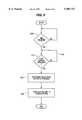
- FIG. 5is a flow diagram of the method of operation of the buffer allocation control device shown in FIG. 3.
- FIG. 2is a block diagram of the preferred embodiment of the present invention.
- Serial data interface 30includes ports 32, 34 that each have integrated receivers 36, 38 and transmitters 40, 42, respectively.
- Preferred bi-directional leads 44 and 46are respective links that are connected to nodes that have an electronic device, such as a disk drive, computer, printer, etc., or other data transmitters or receivers.
- a storage devicesuch as internal frame buffer 50 receives frames from port 32 via lead 52. Internal frame buffer 50 outputs information to port 34 via lead 54. Another storage device, internal frame buffer 60, receives information from port 34 via lead 62, and transmits information to port 32 via lead 64.
- the provision of the cross-coupling of ports 32, 34 with internal frame buffers 50, 60allows for a more efficient frame cut-through between ports 32 and 34.
- NODE 70Internal frame buffers 50, 60 are connected to a NODE 70 via a bi-directional lead 72.
- NODE 70includes circuitry that communicates with other electronic devices, for example, a disk drive and a microprocessor or microcontroller (not shown) through leads 74, 76 and 78. Data can be conveyed between leads 44, 46 and leads 76, 78.
- the term "inbound”is used with respect to a frame transfer from either ports 32 or 34 to NODE 70, and the term “outbound” is used with respect to a frame transfer from NODE 70 to either port 32 or 34. These terms are used relative to the preferred embodiment of the present invention, and are not meant as limitations to the present invention.
- One benefit of having two internal frame buffers 50, 60is that each supports less bandwidth than one frame buffer, such as RAM 10 in FIG. 1.
- Internal frame buffer 50supports the 20 MBytes/sec of leads 52, 54 and 40 MBytes/sec of lead 72 for a total of 80 MBytes/sec.
- internal frame buffer 60supports a total of 60 MBytes/sec.
- Each internal frame buffer 50, 60supports less than the 100 MBytes/sec that RAM 10 must support.
- RAM 10supports the higher bandwidth by having, for example, wider data paths or double-banked structures. This causes RAM 10 to be more expensive than internal buffers 50, 60.
- increasing the bandwidth that internal frame buffers 50, 60 and RAM 10 supportwill cause RAM 10 to still be more expensive than internal buffers 50, 60.
- Providing at least two internal frame buffersprovides a capability to provide 40 MBytes/sec link information transfers.
- frame buffers 50, 60operate completely independent due to the use of the preferred connections to ports 32, 34. This allows the buffer allocation control device 102 to be efficient and not lose any bandwidth during channel switching since ports 32, 34 would not be exposed to the access delay inherent in that double-banked RAM structure.
- FIG. 3illustrates a block diagram for each of internal frame buffers 50, 60 shown in FIG. 2.
- Internal frame buffer 90preferably includes a 176 ⁇ 36 Main RAM (MRAM) 92 that receives preferred address information via a lead 94 from a 9 ⁇ 32 Control RAM (CRAM) 96.
- CRAM 96is connected to a port arbiter 98 via lead 100.
- a buffer allocation control device 102is also included in internal frame buffer 90.
- Port arbiter 98 and buffer allocation control device 102are coupled to respective leads 106 and 108.
- Lead 106conducts signals which are used by port arbiter 98 to determine which channel obtains access to MRAM 92. The signals preferably include arbitration requests for access to MRAM 92, and the CRAM 96 address which contains the address to access MRAM 92.
- Lead 108conducts pool buffer allocation requests from ports 32, 34, the DMA and microprocessor.
- a lead 110is coupled to both MRAM 92 and CRAM 94.
- Lead 110is preferably a 36 bit bus coupled to the two ports of MRAM 92. Data written to and read from MRAM 92 and CRAM 96 are conveyed by lead 110.
- MRAM 92preferably contains all of the frame buffers for the frames except for the link reset frames.
- MRAM 92is a preferred dual-port RAM with one port dedicated to the DMA channel 72 (shown in FIG. 2) and the other port dedicated to the link I/O (ports 32, 34 via leads 52, 54 or 62, 64 as shown in FIG. 2).
- MRAM 92is preferably organized as 176 double or long words (four bytes) with every byte preferably protected by a parity bit which is set if the byte has an even number of 1's. Both MRAM ports operate at 25 MHz for a total of 200 MBytes/sec capability per link.
- the MRAMis functionally divided into the following frame buffers as appears in Table 1 below:
- MRAM 92is accessed through five channels which are preferably time multiplexed into slots through channel arbiter 98 on lead 110.
- the five channelsare for inbound frames from ports 32, 34, outbound frames for ports 32, 34, DMA data frames in and out, automatic DMA SMS handling frames in and out, and microprocessor frames in and out.
- Channel arbiter 98will give access to MRAM 92 and CRAM 96 to the highest priority requesting channel unless that channel is requesting more often than its assigned slot frequency.
- the DMA, inbound port (receiver 36 or 42 of port 32, 34), and outbound port (transmitter 38 or 40 or port 32, 34)each have am actual slot frequency of 1/4 of a total 200 MBytes/sec bandwidth.
- Each pool buffercan be allocated by either port 32 or 34 as an inbound or as an outbound buffer.
- the address field of the frameis not separated from the data field. This requires a maximum of 128 bytes of data plus six bytes of address in MRAM 92 to hold the frame.
- the addressis stripped from the data so that the required storage is 128 bytes maximum for the frame.
- the addressis preferably supplied by the DMA. The number of address bytes in the address field is automatically calculated using the rules of the SSA-PH.
- pool data buffersare always allocated as inbound frame data buffers, especially to avoid deadlock situations where a link receive ready (RR) signal cannot be sent from port 32 or 34.
- RRlink receive ready
- Thisalso maintains the ability for inbound frames to ping-pong.
- "Ping-pong"means that as one pool data buffer is being written, another can be read.
- two additional pool bufferscan be allocated to inbound transfers. This allows up to four inbound buffers at most and two inbound buffers at least.
- two pool buffersare deallocated as soon as possible in reserve for outbound data frames. This maintains the ability for outbound frames to ping-pong during the entire read command.
- Pool data bufferscan be used by the microprocessor to send 128 byte data frames.
- the microprocessorshould first request allocation for a pool data buffer. Once allocated, the microprocessor should fill the pool buffer with an address followed by data. Pool buffers are preferably allocated to the microprocessor with less priority than to inbound and DMA transfers. However, if the DMA is not currently requiring outbound pool buffers, a pool buffer will be allocated to the microprocessor before a fourth pool buffer is allocated for inbound frames. This keeps the microprocessor from being indefinitely locked out of sending its data.
- Each port 32, 34has a control RAM (CRAM) 96 which contains pointers, control bytes, and additional information needed to access MRAM 92.
- CRAM 96is a single-port, latched-based RAM structure.
- CRAM 96operates twice as fast as MRAM 92 so that an access to CRAM 96 is synchronized with an access to MRAM 92.
- Each entry in CRAM 96has a preferred format as illustrated in Table 2 below:
- IPTRinput pointer
- the link CRC bytesmay be partially written into MRAM 92 before the end-of-frame flag is detected. In this case, the IPTR and NBytes bytes are adjusted down to the correct value once the end-of-frame flag is detected.
- the output pointerprovides an address that is used to directly access MRAM 92.
- OPTRis used by channels emptying a selected buffer, such as a data pool buffer, in MRAM 92.
- OPTRis reset to the first address of the frame buffer on the first double word read of each frame buffer. This allows the OPTR to automatically reset itself when a frame buffer must be reread. After each double word is read from the selected frame buffer in MRAM 92, OPTR is incremented by one to the next MRAM 92 address of the selected frame buffer.
- IPTRIPTR is not reset until a selected frame buffer is allocated
- IPTRIPTR is not reset until a selected frame buffer is allocated
- the end-of-frame conditionis recognized.
- OPTRis prevented from having a value that allows access to the "IPTR--1 double word" in order to prevent the outbound channel from sending the link CRC bytes before the IPTR is adjusted down.
- the Control-Byte fieldis loaded with a control byte that corresponds to the frame stored in the selected frame buffer. On inbound frames, this byte is the actual control byte from the link. On outbound frames, the control byte is partially cleared and then modified by hardware with a new transmit sequence number.
- the NBytes fieldspecifies the number of bytes in the frame stored in the selected frame buffer of MRAM 92. As it is incremented, it is checked for too many bytes and end-of-frame conditions.
- a preferred look ahead schemeuses NBytes along with the number of bytes loaded into another inbound buffer to reject the frame when it is too long. When a frame is too long, MRAM 92 is protected from running over into the next buffer of MRAM 92 and the CRAM 96 IPTR/NBytes fields are not incremented. NBytes is adjusted down at the end of inbound frames where the CRC bytes are written to MRAM 92 before the end-of-frame flag is detected. All CRAM 96 fields are preferably self-initializing and do not require the microprocessor to write values on power-up.
- CRAM 96is preferably implemented with latches, and unused bits of some of the other fields of each entry in CRAM 96 are removed to save chip area. These bits should be written as a "0” and should be read as a "0".
- a pool arbiter 120is coupled to an inbound port (receiver 36 or 38 shown in FIG. 2) via leads 122, 124 and 126.
- the pool arbiter 120is also coupled to the DMA via leas 128, 130 and 132, and a microprocessor via leads 134, 136 and 138.
- the pool arbiter 120is coupled to control registers 140 via a lead 142.
- the microprocessoris coupled to control registers 140 via lead 144.
- FLAGS 150is coupled to pool arbiter 120 via leads 152 and 154.
- a counter 160is coupled to pool buffer arbiter 120 via leads 162 and 164.
- a counter 170is coupled to pool buffer arbiter 120 via lead 172 and lead 174 through an inverter 176.
- Counters 160, 170are coupled to FLAGS 150 via respective leads 180 and 182.
- An inverter 184is interposed to FLAGS 150 and counter 170.
- pool buffer arbiter 120waits for a signal REQ. More specific with reference to FIG. 4, pool buffer arbiter 120 receives arbitration request signals REQ from an inbound port, the DMA and microprocessor.
- the inbound portrequires inbound pool data buffers whereas the DMA and microprocessor require outbound pool data buffers.
- pool buffer arbiter 120determines if there is a pool data buffer available, either inbound or outbound depending on who made the request. Referring to FIG. 4, this determination is made by pool buffer arbiter 120 checking control registers 140 to determine, among other things, whether there is a limit set on the pool buffer allocation. Preferably, if a predetermined bit is set in control registers 140, then only two pool buffers can be allocated as inbound buffers. This always guarantees availability of two pool buffers for outbound frame transfers. If the bit is cleared, all four pool buffers can be allocated as inbound buffers when, for example, a DMA read is not active.
- both ports 32, 34operate in the same mode, i.e., whether two or all four pool buffers can be used as inbound buffers.
- the predetermined bit in control registers 140is read from and written to by the microprocessor via lead 144.
- Pool buffer arbiter 120also checks counters 160 and 170 to determine if a pool buffer is available, depending on whether the pool buffer is to be used for inbound or outbound frames.
- pool arbiter 120determines which pool buffer is available. To determine which pool buffers are available, pool buffer arbiter 120 checks FLAGS 150 to determine which pool buffers are allocated. Preferably, FLAGS 150 includes the following information: which pool buffers are currently allocated and whether the microprocessor is allocated a pool buffer, and which one, for use by firmware. Pool buffer arbiter 120 checks for the availability of pool buffers A, B, C and D, in that order. If a pool buffer is not available, the next pool buffer is checked.
- FLAGS 150There are preselected bits in FLAGS 150 that indicate for each pool buffer whether it is currently allocated to either an inbound or outbound transfer. Each bit is set when the corresponding pool buffer is assigned as an inbound or outbound buffer.
- pool buffer arbiter 120waits until one becomes available as shown by line 215 in FIG. 5. If a pool buffer is available, then pool buffer arbiter 120 sets the bit in FLAGS 150 that corresponds to the allocated pool buffer. Pool buffer arbiter also adjusts counters 160, 170 according to whether the allocated pool buffer is for an inbound or outbound frame.
- Pool buffer arbiter 120then performs 230 in FIG. 5.
- Signal ACKacknowledges to the sender that its request is granted.
- Signal BUFis preferably the address to CRAM 96 that contains the address to the allocated pool buffer in MRAM 92.
- a pool bufferis deallocated when a pool buffer allocated to an inbound DMA frame is completely transferred to the DMA.
- a pool bufferis also deallocated when a pool buffer allocated to an inbound DMA frame was received from the link, but the DMA write command was already completed. This may occur due to the initiator providing more frames than were in the command byte count, or due to the direct memory access being aborted during a DMA write command.
- a pool bufferis deallocated when an inbound pool buffer frame had a receiver error. This includes frame reject errors, link CRC errors, protocol errors, and the receipt of abort characters. On an abort, the pool buffer receiving the inbound frame is automatically deallocated by the inbound port. If the inbound frame was sent to the outbound port for a link cut-through, then the outbound pool buffer frame transfer is aborted and the frame is deallocated.
- a pool bufferis deallocated when an inbound pool buffer for the DMA has a zero length data field. Frames without a data field which are destined for the DMA are accepted by the protocol but are deallocated by the frame buffer as soon as the link ACK occurs. However, frames destined for the microprocessor or for cut-through are handled as normal. This frame is discarded and not sent to the DMA.
- a pool bufferis deallocated when an outbound pool buffer from the DMA is aborted by the DMA. This may occur when the DMA read transfer is aborted by either the microprocessor or due to a buffer CRC error. Deallocation also occurs when a Total/Absolute reset frame in the reset buffer is sent to the link.
- Outbound framescan be aborted due to link cut-throughs which are aborted, or by a link error condition.
- the pool buffer involvedis deallocated.
- pool buffers A and Bare allocated to an inbound port and pool buffers C and D are allocated to a DMA read.
- Counters 160 and 170will each have a value of two.
- a minimum of two pool buffersmust be available as inbound buffers.
- the minimum number of pool buffers allocated to any electronic device or other data sourcecan be any value greater than or equal to zero.
- pool buffer arbiter 120checks counter 160. Preferably, this request is given less priority than hardware requests for inbound or outbound pool buffers except when no DMA operation is active. Since there are two pool buffers allocated as outbound, there are no more pool buffers available.
- pool buffer C allocated to the DMAbecomes available.
- the counter 160is adjusted to have a value of one.
- the bit in FLAGS 150 corresponding to pool buffer Cis cleared.
- Pool buffer arbitersenses the value in counter 160 and the cleared bit in FLAGS 150, and allocates pool buffer C to the microprocessor.
- Pool buffer arbiter 120then adjusts the value of counter 160 to two to reflect that there are two pool buffers allocated as outbound buffers. Pool buffer arbiter 120 also sets the bit in FLAGS 150 that corresponds to pool buffer C to reflect that it is allocated. Pool buffer arbiter 120 will also set bits in FLAGS 150 to reflect that pool buffer C is allocated to the microprocessor.
- Pool buffer arbiter 120signals the microprocessor with signal ACK to confer the allocation of pool buffer C and with signal BUF that is the address in CRAM 96 (FIG. 2) which contains the address of pool buffer C in MRAM 92.
- RAM port arbiter 98determines the priority of the requester. Preferably, the microprocessor has less priority than the DMA or inbound port.
- RAM port arbiter 98After the microprocessor is granted access to MRAM 92, RAM port arbiter 98 provides the BUF address to CRAM 96, which in turn outputs an address to MRAM 92 via lead 94. The output address corresponds to the first double-word of pool buffer C. RAM port arbiter 98 also supplies to MRAM 92 signals that enable the microprocessor frame to be written into pool buffer C. RAM port arbiter 98 toggles access to the two ports of MRAM 92, where one port is dedicated to the DMA and SMS automation channels, and the other port is dedicated to inbound and outbound port frames and microprocessor outbound frames. The microprocessor frame is provided to MRAM 92 via lead 110 to the port dedicated to the inbound/outbound frames.
- the microprocessor(requester) initiates a transfer of the frame to the destination port, either 32 or 34. Subsequently, the data is read from pool buffer C.
- the destination portdeallocates pool buffer C by adjusting the counter 160 to a value of one to reflect that there is now a pool buffer available. Furthermore, the relevant bits in FLAGS 150 are cleared by the destination port so that the status of pool buffer C is non-allocated, i.e., the microprocessor does not have a pool buffer allocated to it.
- a pool bufferis allocated to the microprocessor before the fourth inbound pool buffer is allocated to either the inbound port or the DMA.
- the microprocessorrequests allocation for a pool buffer each time it wishes to send a frame.
- Pool buffer allocationbegins for two outbound buffers when a DMA read command starts.
- the allocation for an inbound bufferbegins when a request is received from the link by an initiator and successfully verified.
- the previous discussion about the operation of the buffer allocation controldescribes dynamically allocating the pool buffers.
- One important aspect of the dynamic allocation of the pool buffersis to minimize the average length of time where an outbound or inbound channel (DMA and microprocessor or port) will wait for two buffers to be allocated for its transfer. Having at least two buffers available for either the inbound or outbound channel provides the best performance advantage since one pool buffer can be receiving while the other is transmitting (ping-ponging).
- the minimum number of inbound pool buffersare not allocated as dedicated pool buffers, but are dynamically allocated. Thus, whichever pool buffer is available is allocated subject to the preferred mode that a minimum of two pool buffers are allocated for inbound frames.
- the dynamic allocation of pool buffers for one frame bufferis preferably independent of the dynamic allocation of pool buffers for the other frame buffer.
- the minimum number of pool buffers that are allocated as inboundcan be the same or different for each frame buffer.
- the number of pool buffers for each frame buffercan be the same or different.
- a further advantage of the present inventionis that the use of two MRAMs each having pool buffers allows for all four buffers of one MRAM to be used for inbound frames from a port and allows for two pool buffers from the other MRAM to be used for outbound frames to that port. In this manner, the SSA can be concurrently receiving from and transmitting to the same link via one port even after two inbound buffers have been allocated.
- Pool buffer arbiter 120then includes circuitry that determines how many pool buffers are allocated as inbound and outbound by checking the status of the pool buffers in FLAGS 150.
- FLAGS 150can include circuitry to store which device (DMA or inbound port) is allocated to which pool buffer.
Landscapes
- Engineering & Computer Science (AREA)
- Computer Networks & Wireless Communication (AREA)
- Signal Processing (AREA)
- Computer And Data Communications (AREA)
- Communication Control (AREA)
Abstract
Description
TABLE 1______________________________________FirmwareOutbound Message 40 bytesHardwareOutbound Message 32 bytesReset 8 bytesInbound Message A 40 bytesInbound Message B 40 bytesPool A 136bytesPool B 136bytesPool C 136bytesPool D 136 bytes______________________________________
TABLE 2______________________________________ Control-IPTR OPTR Byte NBytes______________________________________1 byte 1 byte 1 byte 1 byte______________________________________
Claims (8)
Priority Applications (5)
| Application Number | Priority Date | Filing Date | Title |
|---|---|---|---|
| US08/605,965US5907717A (en) | 1996-02-23 | 1996-02-23 | Cross-connected memory system for allocating pool buffers in each frame buffer and providing addresses thereof |
| DE69735936TDE69735936T2 (en) | 1996-02-23 | 1997-02-24 | SERIAL DATA INTERFACE PROCESS AND DEVICE # |
| EP97905272AEP0882343B1 (en) | 1996-02-23 | 1997-02-24 | Serial data interface method and apparatus |
| PCT/GB1997/000527WO1997033410A1 (en) | 1996-02-23 | 1997-02-24 | Serial data interface method and apparatus |
| AU18885/97AAU1888597A (en) | 1996-02-23 | 1997-02-24 | Serial data interface method and apparatus |
Applications Claiming Priority (1)
| Application Number | Priority Date | Filing Date | Title |
|---|---|---|---|
| US08/605,965US5907717A (en) | 1996-02-23 | 1996-02-23 | Cross-connected memory system for allocating pool buffers in each frame buffer and providing addresses thereof |
Publications (1)
| Publication Number | Publication Date |
|---|---|
| US5907717Atrue US5907717A (en) | 1999-05-25 |
Family
ID=24425957
Family Applications (1)
| Application Number | Title | Priority Date | Filing Date |
|---|---|---|---|
| US08/605,965Expired - LifetimeUS5907717A (en) | 1996-02-23 | 1996-02-23 | Cross-connected memory system for allocating pool buffers in each frame buffer and providing addresses thereof |
Country Status (5)
| Country | Link |
|---|---|
| US (1) | US5907717A (en) |
| EP (1) | EP0882343B1 (en) |
| AU (1) | AU1888597A (en) |
| DE (1) | DE69735936T2 (en) |
| WO (1) | WO1997033410A1 (en) |
Cited By (42)
| Publication number | Priority date | Publication date | Assignee | Title |
|---|---|---|---|---|
| US6038621A (en)* | 1996-11-04 | 2000-03-14 | Hewlett-Packard Company | Dynamic peripheral control of I/O buffers in peripherals with modular I/O |
| US6223261B1 (en)* | 1997-07-31 | 2001-04-24 | Matsushita Electric Industrial Co., Ltd. | Communication system method and recording apparatus for performing arbitrary application processing |
| US6304920B1 (en)* | 1997-01-14 | 2001-10-16 | Mitsumi Electric Co., Ltd. | Switching means for directly controlling operation of data storage devices, data storage/reproducing devices, and data reproducing devices |
| US6330626B1 (en)* | 1999-05-05 | 2001-12-11 | Qlogic Corporation | Systems and methods for a disk controller memory architecture |
| US6401149B1 (en)* | 1999-05-05 | 2002-06-04 | Qlogic Corporation | Methods for context switching within a disk controller |
| US6421756B1 (en)* | 1999-05-06 | 2002-07-16 | International Business Machines Corporation | Buffer assignment for bridges |
| US6539504B1 (en)* | 1996-08-30 | 2003-03-25 | Siemens Aktiengesellschaft | Memory system having error monitoring apparatus for multi-bit errors |
| US20030084255A1 (en)* | 2001-10-29 | 2003-05-01 | Yoshito Suzuki | Memory control circuit and method for arbitrating memory bus |
| US20030126132A1 (en)* | 2001-12-27 | 2003-07-03 | Kavuri Ravi K. | Virtual volume management system and method |
| US20030177293A1 (en)* | 2002-03-12 | 2003-09-18 | International Business Machines Corporation | Dynamic memory allocation between inbound and outbound buffers in a protocol handler |
| US6646948B1 (en) | 2002-08-29 | 2003-11-11 | Motorola, Inc. | Data storage system utilizing a non-volatile IC based memory for reduction of data retrieval time |
| US6791989B1 (en)* | 1999-12-30 | 2004-09-14 | Agilent Technologies, Inc. | Fibre channel interface controller that performs non-blocking output and input of fibre channel data frames and acknowledgement frames to and from a fibre channel |
| US20040193743A1 (en)* | 2003-03-10 | 2004-09-30 | Byers Larry L. | Servo controller interface module for embedded disk controllers |
| US20040199718A1 (en)* | 2003-03-10 | 2004-10-07 | Byers Larry L. | Method and system for embedded disk controllers |
| USRE38650E1 (en)* | 1996-07-01 | 2004-11-09 | Sun Microsystems, Inc. | System for performing deadlock free message transfer in cyclic multi-hop digital computer network using a number of buffers based on predetermined diameter |
| US20050078695A1 (en)* | 2003-06-27 | 2005-04-14 | Broadcom Corporation | Dynamically shared memory |
| US20050174680A1 (en)* | 2004-02-10 | 2005-08-11 | Spaur Michael R. | Method and system for head position control in embedded disk drive controllers |
| US20050276151A1 (en)* | 2004-06-14 | 2005-12-15 | White Theodore C | Integrated memory controller |
| US20050289261A1 (en)* | 2004-06-28 | 2005-12-29 | White Theodore C | System and method for reading and writing data using storage controllers |
| US20060015774A1 (en)* | 2004-07-19 | 2006-01-19 | Nguyen Huy T | System and method for transmitting data in storage controllers |
| US20060015660A1 (en)* | 2004-07-19 | 2006-01-19 | Kha Nguyen | System and method for controlling buffer memory overflow and underflow conditions in storage controllers |
| US20060015654A1 (en)* | 2004-07-19 | 2006-01-19 | Krantz Leon A | Dynamic WWN module for storage controllers |
| US7006318B2 (en) | 2002-08-29 | 2006-02-28 | Freescale Semiconductor, Inc. | Removable media storage system with memory for storing operational data |
| US7007114B1 (en) | 2003-01-31 | 2006-02-28 | Qlogic Corporation | System and method for padding data blocks and/or removing padding from data blocks in storage controllers |
| US7020712B1 (en)* | 1998-09-30 | 2006-03-28 | Cisco Technology, Inc. | Reducing CPU overhead in the forwarding process in an inbound/outbound controller for a router |
| US7039771B1 (en) | 2003-03-10 | 2006-05-02 | Marvell International Ltd. | Method and system for supporting multiple external serial port devices using a serial port controller in embedded disk controllers |
| US20060104269A1 (en)* | 2004-11-15 | 2006-05-18 | Perozo Angel G | Method and system for processing frames in storage controllers |
| US20060117235A1 (en)* | 2004-11-08 | 2006-06-01 | Dinesh Jayabharathi | System and method for conducting BIST operations |
| US20060129704A1 (en)* | 2003-03-10 | 2006-06-15 | Byers Larry L | Method and system for monitoring embedded disk controller components |
| US7064915B1 (en) | 2003-03-10 | 2006-06-20 | Marvell International Ltd. | Method and system for collecting servo field data from programmable devices in embedded disk controllers |
| US7096378B2 (en) | 2002-08-29 | 2006-08-22 | Freescale Semiconductor, Inc. | Data storage system having a non-volatile IC based memory for storing user data |
| US7111228B1 (en) | 2002-05-07 | 2006-09-19 | Marvell International Ltd. | System and method for performing parity checks in disk storage system |
| US20060227447A1 (en)* | 2005-04-06 | 2006-10-12 | Pinvidic Daniel R | Method and system for read gate timing control for storage controllers |
| US7287102B1 (en) | 2003-01-31 | 2007-10-23 | Marvell International Ltd. | System and method for concatenating data |
| US7386661B2 (en) | 2004-10-13 | 2008-06-10 | Marvell International Ltd. | Power save module for storage controllers |
| US7492545B1 (en) | 2003-03-10 | 2009-02-17 | Marvell International Ltd. | Method and system for automatic time base adjustment for disk drive servo controllers |
| US7526691B1 (en) | 2003-10-15 | 2009-04-28 | Marvell International Ltd. | System and method for using TAP controllers |
| US20090157913A1 (en)* | 2007-12-18 | 2009-06-18 | Bellows Gregory H | Method for Toggling Non-Adjacent Channel Identifiers During DMA Double Buffering Operations |
| US20130222210A1 (en)* | 2012-02-28 | 2013-08-29 | Qualcomm Incorporated | Frame capture and buffering at source device in wireless display system |
| US9229791B1 (en)* | 2012-08-24 | 2016-01-05 | Qlogic, Corporation | System and method for high speed multiple buffer allocation |
| US20160232112A1 (en)* | 2015-02-06 | 2016-08-11 | Futurewei Technologies, Inc. | Unified Memory Bus and Method to Operate the Unified Memory Bus |
| US20200042475A1 (en)* | 2018-07-31 | 2020-02-06 | Nutanix, Inc. | Elastic method of remote direct memory access memory advertisement |
Citations (34)
| Publication number | Priority date | Publication date | Assignee | Title |
|---|---|---|---|---|
| US3924245A (en)* | 1973-07-18 | 1975-12-02 | Int Computers Ltd | Stack mechanism for a data processor |
| US4158235A (en)* | 1977-04-18 | 1979-06-12 | Burroughs Corporation | Multi port time-shared associative buffer storage pool |
| US4509119A (en)* | 1982-06-24 | 1985-04-02 | International Business Machines Corporation | Method for managing a buffer pool referenced by batch and interactive processes |
| US4554659A (en)* | 1983-12-12 | 1985-11-19 | At&T Bell Laboratories | Data communication network |
| US4644529A (en)* | 1985-08-02 | 1987-02-17 | Gte Laboratories Incorporated | High-speed switching processor for a burst-switching communications system |
| EP0272939A2 (en)* | 1986-12-23 | 1988-06-29 | Oki Electric Industry Company, Limited | Dynamic buffer supervising system for a data link access protocol control |
| EP0372765A2 (en)* | 1988-12-02 | 1990-06-13 | Advanced Micro Devices, Inc. | Methods and apparatus for performing restricted token operations on an FDDI network |
| US5093912A (en)* | 1989-06-26 | 1992-03-03 | International Business Machines Corporation | Dynamic resource pool expansion and contraction in multiprocessing environments |
| US5161215A (en)* | 1986-06-02 | 1992-11-03 | Hitachi, Ltd. | Method for controlling data transfer buffer |
| AU2856292A (en)* | 1991-11-29 | 1993-06-03 | American Telephone And Telegraph Company | Multiple virtual fifo arrangement |
| US5233606A (en)* | 1991-08-02 | 1993-08-03 | At&T Bell Laboratories | Arrangement for controlling shared-buffer-memory overflow in a multi-priority environment |
| US5233603A (en)* | 1988-04-21 | 1993-08-03 | Nec Corporation | Packet switch suitable for integrated circuit implementation |
| US5237661A (en)* | 1989-05-29 | 1993-08-17 | Hitachi, Ltd. | Buffer management method and system therefor using an I/O buffer on main memory and utilizing virtual memory and page fixing |
| US5278828A (en)* | 1992-06-04 | 1994-01-11 | Bell Communications Research, Inc. | Method and system for managing queued cells |
| US5287346A (en)* | 1991-10-16 | 1994-02-15 | Carnegie Mellon University | Packet switch |
| US5289470A (en)* | 1992-12-14 | 1994-02-22 | International Business Machines Corp. | Flexible scheme for buffer space allocation in networking devices |
| US5291482A (en)* | 1992-07-24 | 1994-03-01 | At&T Bell Laboratories | High bandwidth packet switch |
| US5315707A (en)* | 1992-01-10 | 1994-05-24 | Digital Equipment Corporation | Multiprocessor buffer system |
| US5327422A (en)* | 1991-12-16 | 1994-07-05 | Telefonaktiebolaget L M Ericsson | Controllable multiplexer for a digital switch |
| US5333269A (en)* | 1988-10-28 | 1994-07-26 | International Business Machines Corporation | Mechanism for transferring messages between source and destination users through a shared memory |
| US5367643A (en)* | 1991-02-06 | 1994-11-22 | International Business Machines Corporation | Generic high bandwidth adapter having data packet memory configured in three level hierarchy for temporary storage of variable length data packets |
| US5406556A (en)* | 1992-06-05 | 1995-04-11 | Widjaja; Indra | Output buffered packet switch with a flexible buffer management scheme |
| US5412781A (en)* | 1991-06-06 | 1995-05-02 | Siemens Aktiengesellschaft | Method and arrangement of buffer allocation in communication systems by employing fixed and dynamic buffer allocation functions |
| US5432908A (en)* | 1991-07-10 | 1995-07-11 | International Business Machines Corporation | High speed buffer management of share memory using linked lists and plural buffer managers for processing multiple requests concurrently |
| US5440545A (en)* | 1993-08-02 | 1995-08-08 | Motorola, Inc. | Packet delivery system |
| US5483578A (en)* | 1993-10-08 | 1996-01-09 | Alcatel Sel Aktiengesellschaft | Method of managing a speech memory, and assembly therefor |
| US5530871A (en)* | 1993-09-29 | 1996-06-25 | Nec Corporation | Asynchronous input and output control system |
| US5535364A (en)* | 1993-04-12 | 1996-07-09 | Hewlett-Packard Company | Adaptive method for dynamic allocation of random access memory to procedures having differing priorities based on first and second threshold levels of free RAM |
| US5553073A (en)* | 1993-05-17 | 1996-09-03 | Ibm Corporation | Token ring network |
| US5572645A (en)* | 1994-03-01 | 1996-11-05 | International Business Machines Corporation | Buffer management policy for an on-demand video server |
| US5572697A (en)* | 1992-01-17 | 1996-11-05 | International Business Machines Corporation | Apparatus for recovering lost buffer contents in a data processing system |
| US5617537A (en)* | 1993-10-05 | 1997-04-01 | Nippon Telegraph And Telephone Corporation | Message passing system for distributed shared memory multiprocessor system and message passing method using the same |
| US5680551A (en)* | 1993-10-21 | 1997-10-21 | Sybase, Inc. | Electronic messaging method of and system for heterogeneous connectivity and universal and generic interfacing for distributed applications and processes residing in wide variety of computing platforms and communication transport facilities |
| US5802351A (en)* | 1995-02-14 | 1998-09-01 | Nokia Mobile Phones Limited | Data interface |
- 1996
- 1996-02-23USUS08/605,965patent/US5907717A/ennot_activeExpired - Lifetime
- 1997
- 1997-02-24AUAU18885/97Apatent/AU1888597A/ennot_activeAbandoned
- 1997-02-24EPEP97905272Apatent/EP0882343B1/ennot_activeExpired - Lifetime
- 1997-02-24DEDE69735936Tpatent/DE69735936T2/ennot_activeExpired - Lifetime
- 1997-02-24WOPCT/GB1997/000527patent/WO1997033410A1/enactiveIP Right Grant
Patent Citations (36)
| Publication number | Priority date | Publication date | Assignee | Title |
|---|---|---|---|---|
| US3924245A (en)* | 1973-07-18 | 1975-12-02 | Int Computers Ltd | Stack mechanism for a data processor |
| US4158235A (en)* | 1977-04-18 | 1979-06-12 | Burroughs Corporation | Multi port time-shared associative buffer storage pool |
| US4509119A (en)* | 1982-06-24 | 1985-04-02 | International Business Machines Corporation | Method for managing a buffer pool referenced by batch and interactive processes |
| US4554659A (en)* | 1983-12-12 | 1985-11-19 | At&T Bell Laboratories | Data communication network |
| US4644529A (en)* | 1985-08-02 | 1987-02-17 | Gte Laboratories Incorporated | High-speed switching processor for a burst-switching communications system |
| US5161215A (en)* | 1986-06-02 | 1992-11-03 | Hitachi, Ltd. | Method for controlling data transfer buffer |
| US4845710A (en)* | 1986-12-23 | 1989-07-04 | Oki Electric Industry Co., Ltd. | Dynamic buffer supervising system for a data link access protocol control |
| EP0272939A2 (en)* | 1986-12-23 | 1988-06-29 | Oki Electric Industry Company, Limited | Dynamic buffer supervising system for a data link access protocol control |
| US5233603A (en)* | 1988-04-21 | 1993-08-03 | Nec Corporation | Packet switch suitable for integrated circuit implementation |
| US5333269A (en)* | 1988-10-28 | 1994-07-26 | International Business Machines Corporation | Mechanism for transferring messages between source and destination users through a shared memory |
| EP0372765A2 (en)* | 1988-12-02 | 1990-06-13 | Advanced Micro Devices, Inc. | Methods and apparatus for performing restricted token operations on an FDDI network |
| US5237661A (en)* | 1989-05-29 | 1993-08-17 | Hitachi, Ltd. | Buffer management method and system therefor using an I/O buffer on main memory and utilizing virtual memory and page fixing |
| US5093912A (en)* | 1989-06-26 | 1992-03-03 | International Business Machines Corporation | Dynamic resource pool expansion and contraction in multiprocessing environments |
| US5367643A (en)* | 1991-02-06 | 1994-11-22 | International Business Machines Corporation | Generic high bandwidth adapter having data packet memory configured in three level hierarchy for temporary storage of variable length data packets |
| US5412781A (en)* | 1991-06-06 | 1995-05-02 | Siemens Aktiengesellschaft | Method and arrangement of buffer allocation in communication systems by employing fixed and dynamic buffer allocation functions |
| US5432908A (en)* | 1991-07-10 | 1995-07-11 | International Business Machines Corporation | High speed buffer management of share memory using linked lists and plural buffer managers for processing multiple requests concurrently |
| US5233606A (en)* | 1991-08-02 | 1993-08-03 | At&T Bell Laboratories | Arrangement for controlling shared-buffer-memory overflow in a multi-priority environment |
| US5287346A (en)* | 1991-10-16 | 1994-02-15 | Carnegie Mellon University | Packet switch |
| EP0545575A1 (en)* | 1991-11-29 | 1993-06-09 | AT&T Corp. | Multiple virtual FIFO arrangement |
| AU2856292A (en)* | 1991-11-29 | 1993-06-03 | American Telephone And Telegraph Company | Multiple virtual fifo arrangement |
| US5327422A (en)* | 1991-12-16 | 1994-07-05 | Telefonaktiebolaget L M Ericsson | Controllable multiplexer for a digital switch |
| US5315707A (en)* | 1992-01-10 | 1994-05-24 | Digital Equipment Corporation | Multiprocessor buffer system |
| US5572697A (en)* | 1992-01-17 | 1996-11-05 | International Business Machines Corporation | Apparatus for recovering lost buffer contents in a data processing system |
| US5278828A (en)* | 1992-06-04 | 1994-01-11 | Bell Communications Research, Inc. | Method and system for managing queued cells |
| US5406556A (en)* | 1992-06-05 | 1995-04-11 | Widjaja; Indra | Output buffered packet switch with a flexible buffer management scheme |
| US5291482A (en)* | 1992-07-24 | 1994-03-01 | At&T Bell Laboratories | High bandwidth packet switch |
| US5289470A (en)* | 1992-12-14 | 1994-02-22 | International Business Machines Corp. | Flexible scheme for buffer space allocation in networking devices |
| US5535364A (en)* | 1993-04-12 | 1996-07-09 | Hewlett-Packard Company | Adaptive method for dynamic allocation of random access memory to procedures having differing priorities based on first and second threshold levels of free RAM |
| US5553073A (en)* | 1993-05-17 | 1996-09-03 | Ibm Corporation | Token ring network |
| US5440545A (en)* | 1993-08-02 | 1995-08-08 | Motorola, Inc. | Packet delivery system |
| US5530871A (en)* | 1993-09-29 | 1996-06-25 | Nec Corporation | Asynchronous input and output control system |
| US5617537A (en)* | 1993-10-05 | 1997-04-01 | Nippon Telegraph And Telephone Corporation | Message passing system for distributed shared memory multiprocessor system and message passing method using the same |
| US5483578A (en)* | 1993-10-08 | 1996-01-09 | Alcatel Sel Aktiengesellschaft | Method of managing a speech memory, and assembly therefor |
| US5680551A (en)* | 1993-10-21 | 1997-10-21 | Sybase, Inc. | Electronic messaging method of and system for heterogeneous connectivity and universal and generic interfacing for distributed applications and processes residing in wide variety of computing platforms and communication transport facilities |
| US5572645A (en)* | 1994-03-01 | 1996-11-05 | International Business Machines Corporation | Buffer management policy for an on-demand video server |
| US5802351A (en)* | 1995-02-14 | 1998-09-01 | Nokia Mobile Phones Limited | Data interface |
Non-Patent Citations (2)
| Title |
|---|
| IBM Technical Disclosure Bulletin; ATM Switch with Cut Through Shared Buffers; vol. 37 No. 05; May 1994.* |
| IBM Technical Disclosure Bulletin; ATM Switch with Cut-Through Shared Buffers; vol. 37 No. 05; May 1994. |
Cited By (93)
| Publication number | Priority date | Publication date | Assignee | Title |
|---|---|---|---|---|
| USRE38650E1 (en)* | 1996-07-01 | 2004-11-09 | Sun Microsystems, Inc. | System for performing deadlock free message transfer in cyclic multi-hop digital computer network using a number of buffers based on predetermined diameter |
| US6539504B1 (en)* | 1996-08-30 | 2003-03-25 | Siemens Aktiengesellschaft | Memory system having error monitoring apparatus for multi-bit errors |
| US6038621A (en)* | 1996-11-04 | 2000-03-14 | Hewlett-Packard Company | Dynamic peripheral control of I/O buffers in peripherals with modular I/O |
| US6304920B1 (en)* | 1997-01-14 | 2001-10-16 | Mitsumi Electric Co., Ltd. | Switching means for directly controlling operation of data storage devices, data storage/reproducing devices, and data reproducing devices |
| US6223261B1 (en)* | 1997-07-31 | 2001-04-24 | Matsushita Electric Industrial Co., Ltd. | Communication system method and recording apparatus for performing arbitrary application processing |
| US7020712B1 (en)* | 1998-09-30 | 2006-03-28 | Cisco Technology, Inc. | Reducing CPU overhead in the forwarding process in an inbound/outbound controller for a router |
| US6330626B1 (en)* | 1999-05-05 | 2001-12-11 | Qlogic Corporation | Systems and methods for a disk controller memory architecture |
| US6401149B1 (en)* | 1999-05-05 | 2002-06-04 | Qlogic Corporation | Methods for context switching within a disk controller |
| US6421756B1 (en)* | 1999-05-06 | 2002-07-16 | International Business Machines Corporation | Buffer assignment for bridges |
| US6791989B1 (en)* | 1999-12-30 | 2004-09-14 | Agilent Technologies, Inc. | Fibre channel interface controller that performs non-blocking output and input of fibre channel data frames and acknowledgement frames to and from a fibre channel |
| US20030084255A1 (en)* | 2001-10-29 | 2003-05-01 | Yoshito Suzuki | Memory control circuit and method for arbitrating memory bus |
| US6754786B2 (en)* | 2001-10-29 | 2004-06-22 | Mitsubishi Denki Kabushiki Kaisha | Memory control circuit and method for arbitrating memory bus |
| US20030126132A1 (en)* | 2001-12-27 | 2003-07-03 | Kavuri Ravi K. | Virtual volume management system and method |
| US6877048B2 (en)* | 2002-03-12 | 2005-04-05 | International Business Machines Corporation | Dynamic memory allocation between inbound and outbound buffers in a protocol handler |
| US20070156931A1 (en)* | 2002-03-12 | 2007-07-05 | International Business Machines Corporation | Dynamic memory allocation between inbound and outbound buffers in a protocol handler |
| US7739427B2 (en) | 2002-03-12 | 2010-06-15 | International Business Machines Corporation | Dynamic memory allocation between inbound and outbound buffers in a protocol handler |
| US20030177293A1 (en)* | 2002-03-12 | 2003-09-18 | International Business Machines Corporation | Dynamic memory allocation between inbound and outbound buffers in a protocol handler |
| US7249206B2 (en)* | 2002-03-12 | 2007-07-24 | International Business Machines Corporation | Dynamic memory allocation between inbound and outbound buffers in a protocol handler |
| US20040233924A1 (en)* | 2002-03-12 | 2004-11-25 | International Business Machines Corporation | Dynamic memory allocation between inbound and outbound buffers in a protocol handler |
| US7457895B2 (en) | 2002-03-12 | 2008-11-25 | International Business Machines Corporation | Dynamic memory allocation between inbound and outbound buffers in a protocol handler |
| US7559009B1 (en) | 2002-05-07 | 2009-07-07 | Marvell International, Ltd. | System and method for performing parity checks in disk storage systems |
| US7111228B1 (en) | 2002-05-07 | 2006-09-19 | Marvell International Ltd. | System and method for performing parity checks in disk storage system |
| US6646948B1 (en) | 2002-08-29 | 2003-11-11 | Motorola, Inc. | Data storage system utilizing a non-volatile IC based memory for reduction of data retrieval time |
| US7096378B2 (en) | 2002-08-29 | 2006-08-22 | Freescale Semiconductor, Inc. | Data storage system having a non-volatile IC based memory for storing user data |
| US7006318B2 (en) | 2002-08-29 | 2006-02-28 | Freescale Semiconductor, Inc. | Removable media storage system with memory for storing operational data |
| US7287102B1 (en) | 2003-01-31 | 2007-10-23 | Marvell International Ltd. | System and method for concatenating data |
| US8713224B2 (en) | 2003-01-31 | 2014-04-29 | Marvell International Ltd. | System and method for transferring data in storage controllers |
| US20060129715A1 (en)* | 2003-01-31 | 2006-06-15 | White Theodore C | System and method for transferring data in storage controllers |
| US7007114B1 (en) | 2003-01-31 | 2006-02-28 | Qlogic Corporation | System and method for padding data blocks and/or removing padding from data blocks in storage controllers |
| US7870346B2 (en) | 2003-03-10 | 2011-01-11 | Marvell International Ltd. | Servo controller interface module for embedded disk controllers |
| US7039771B1 (en) | 2003-03-10 | 2006-05-02 | Marvell International Ltd. | Method and system for supporting multiple external serial port devices using a serial port controller in embedded disk controllers |
| US20040193743A1 (en)* | 2003-03-10 | 2004-09-30 | Byers Larry L. | Servo controller interface module for embedded disk controllers |
| US8189285B1 (en) | 2003-03-10 | 2012-05-29 | Marvell International Ltd. | Method and system for automatic time base adjustment for disk drive servo controllers |
| US20060129704A1 (en)* | 2003-03-10 | 2006-06-15 | Byers Larry L | Method and system for monitoring embedded disk controller components |
| US7492545B1 (en) | 2003-03-10 | 2009-02-17 | Marvell International Ltd. | Method and system for automatic time base adjustment for disk drive servo controllers |
| US7064915B1 (en) | 2003-03-10 | 2006-06-20 | Marvell International Ltd. | Method and system for collecting servo field data from programmable devices in embedded disk controllers |
| US7080188B2 (en) | 2003-03-10 | 2006-07-18 | Marvell International Ltd. | Method and system for embedded disk controllers |
| US7975110B1 (en) | 2003-03-10 | 2011-07-05 | Marvell International Ltd. | Method and system for supporting multiple external serial port devices using a serial port controller in embedded disk controllers |
| US7870320B1 (en) | 2003-03-10 | 2011-01-11 | Marvell International Ltd. | Interrupt controller for prioritizing interrupt requests in an embedded disk controller |
| US7457903B2 (en) | 2003-03-10 | 2008-11-25 | Marvell International Ltd. | Interrupt controller for processing fast and regular interrupts |
| US20040199718A1 (en)* | 2003-03-10 | 2004-10-07 | Byers Larry L. | Method and system for embedded disk controllers |
| US20060230214A1 (en)* | 2003-03-10 | 2006-10-12 | Marvell International Ltd. | Method and system for embedded disk controllers |
| US20040199711A1 (en)* | 2003-03-10 | 2004-10-07 | Byers Larry L. | Method and system for using an external bus controller in embedded disk controllers |
| US7336435B1 (en) | 2003-03-10 | 2008-02-26 | Marvell International, Ltd. | Method and system for collecting servo field data from programmable devices in embedded disk controllers |
| US7219182B2 (en) | 2003-03-10 | 2007-05-15 | Marvell International Ltd. | Method and system for using an external bus controller in embedded disk controllers |
| US7853747B2 (en) | 2003-03-10 | 2010-12-14 | Marvell International Ltd. | Method and system for using an external bus controller in embedded disk controllers |
| US20040199695A1 (en)* | 2003-03-10 | 2004-10-07 | Purdham David M. | Method and system for using an interrupt controller in an embedded disk controller |
| US20070226392A1 (en)* | 2003-03-10 | 2007-09-27 | Byers Larry L | Method and system for using an external bus controller in embedded disk controllers |
| US20050078695A1 (en)* | 2003-06-27 | 2005-04-14 | Broadcom Corporation | Dynamically shared memory |
| US7284076B2 (en)* | 2003-06-27 | 2007-10-16 | Broadcom Corporation | Dynamically shared memory |
| US7526691B1 (en) | 2003-10-15 | 2009-04-28 | Marvell International Ltd. | System and method for using TAP controllers |
| US20050174680A1 (en)* | 2004-02-10 | 2005-08-11 | Spaur Michael R. | Method and system for head position control in embedded disk drive controllers |
| US20070053099A1 (en)* | 2004-02-10 | 2007-03-08 | Marvell International Ltd. | Method and system for head position control in embedded disk drive controllers |
| US7139150B2 (en) | 2004-02-10 | 2006-11-21 | Marvell International Ltd. | Method and system for head position control in embedded disk drive controllers |
| US7471485B2 (en) | 2004-02-10 | 2008-12-30 | Marvell International Ltd. | Method and system for head position control in embedded disk drive controllers |
| US8116026B2 (en) | 2004-02-10 | 2012-02-14 | Marvell International Ltd. | Method and system for head position control in embedded disk drive controllers |
| US20090097157A1 (en)* | 2004-02-10 | 2009-04-16 | Spaur Michael R | Method and system for head position control in embedded disk drive controllers |
| US20050276151A1 (en)* | 2004-06-14 | 2005-12-15 | White Theodore C | Integrated memory controller |
| US7120084B2 (en) | 2004-06-14 | 2006-10-10 | Marvell International Ltd. | Integrated memory controller |
| US7286441B1 (en) | 2004-06-14 | 2007-10-23 | Marvell International Ltd. | Integrated memory controller |
| US7535791B1 (en) | 2004-06-14 | 2009-05-19 | Marvell International Ltd. | Integrated memory controller |
| US7596053B1 (en) | 2004-06-14 | 2009-09-29 | Marvell International Ltd. | Integrated memory controller |
| US20050289261A1 (en)* | 2004-06-28 | 2005-12-29 | White Theodore C | System and method for reading and writing data using storage controllers |
| US8166217B2 (en) | 2004-06-28 | 2012-04-24 | Marvell International Ltd. | System and method for reading and writing data using storage controllers |
| US20060015774A1 (en)* | 2004-07-19 | 2006-01-19 | Nguyen Huy T | System and method for transmitting data in storage controllers |
| US9201599B2 (en) | 2004-07-19 | 2015-12-01 | Marvell International Ltd. | System and method for transmitting data in storage controllers |
| US7984252B2 (en) | 2004-07-19 | 2011-07-19 | Marvell International Ltd. | Storage controllers with dynamic WWN storage modules and methods for managing data and connections between a host and a storage device |
| US8032674B2 (en) | 2004-07-19 | 2011-10-04 | Marvell International Ltd. | System and method for controlling buffer memory overflow and underflow conditions in storage controllers |
| US7757009B2 (en) | 2004-07-19 | 2010-07-13 | Marvell International Ltd. | Storage controllers with dynamic WWN storage modules and methods for managing data and connections between a host and a storage device |
| US20060015660A1 (en)* | 2004-07-19 | 2006-01-19 | Kha Nguyen | System and method for controlling buffer memory overflow and underflow conditions in storage controllers |
| US20060015654A1 (en)* | 2004-07-19 | 2006-01-19 | Krantz Leon A | Dynamic WWN module for storage controllers |
| US7386661B2 (en) | 2004-10-13 | 2008-06-10 | Marvell International Ltd. | Power save module for storage controllers |
| US8417900B1 (en) | 2004-10-13 | 2013-04-09 | Marvell International Ltd. | Power save module for storage controllers |
| US7240267B2 (en) | 2004-11-08 | 2007-07-03 | Marvell International Ltd. | System and method for conducting BIST operations |
| US20060117235A1 (en)* | 2004-11-08 | 2006-06-01 | Dinesh Jayabharathi | System and method for conducting BIST operations |
| US8015448B2 (en) | 2004-11-08 | 2011-09-06 | Marvell International Ltd. | System and method for conducting BIST operations |
| US20060104269A1 (en)* | 2004-11-15 | 2006-05-18 | Perozo Angel G | Method and system for processing frames in storage controllers |
| US20110022758A1 (en)* | 2004-11-15 | 2011-01-27 | Perozo Angel G | Method and system for processing frames in storage controllers |
| US7802026B2 (en) | 2004-11-15 | 2010-09-21 | Marvell International Ltd. | Method and system for processing frames in storage controllers |
| US8370541B2 (en) | 2004-11-15 | 2013-02-05 | Marvell International Ltd. | Method and system for processing frames in storage controllers |
| US8023217B1 (en) | 2005-04-06 | 2011-09-20 | Marvell International Ltd. | Method and system for read gate timing control for storage controllers |
| US20060227447A1 (en)* | 2005-04-06 | 2006-10-12 | Pinvidic Daniel R | Method and system for read gate timing control for storage controllers |
| US7609468B2 (en) | 2005-04-06 | 2009-10-27 | Marvell International Ltd. | Method and system for read gate timing control for storage controllers |
| US7689734B2 (en)* | 2007-12-18 | 2010-03-30 | International Business Machines Corporation | Method for toggling non-adjacent channel identifiers during DMA double buffering operations |
| US20090157913A1 (en)* | 2007-12-18 | 2009-06-18 | Bellows Gregory H | Method for Toggling Non-Adjacent Channel Identifiers During DMA Double Buffering Operations |
| CN104137562A (en)* | 2012-02-28 | 2014-11-05 | 高通股份有限公司 | Frame capture and buffering at source device in wireless display system |
| US20130222210A1 (en)* | 2012-02-28 | 2013-08-29 | Qualcomm Incorporated | Frame capture and buffering at source device in wireless display system |
| US9491505B2 (en)* | 2012-02-28 | 2016-11-08 | Qualcomm Incorporated | Frame capture and buffering at source device in wireless display system |
| CN104137562B (en)* | 2012-02-28 | 2017-10-31 | 高通股份有限公司 | The frame-grab at source device and caching in wireless display system |
| US9229791B1 (en)* | 2012-08-24 | 2016-01-05 | Qlogic, Corporation | System and method for high speed multiple buffer allocation |
| US20160232112A1 (en)* | 2015-02-06 | 2016-08-11 | Futurewei Technologies, Inc. | Unified Memory Bus and Method to Operate the Unified Memory Bus |
| US20200042475A1 (en)* | 2018-07-31 | 2020-02-06 | Nutanix, Inc. | Elastic method of remote direct memory access memory advertisement |
| US10824369B2 (en)* | 2018-07-31 | 2020-11-03 | Nutanix, Inc. | Elastic method of remote direct memory access memory advertisement |
Also Published As
| Publication number | Publication date |
|---|---|
| EP0882343A1 (en) | 1998-12-09 |
| AU1888597A (en) | 1997-09-22 |
| EP0882343B1 (en) | 2006-05-24 |
| DE69735936D1 (en) | 2006-06-29 |
| WO1997033410A1 (en) | 1997-09-12 |
| DE69735936T2 (en) | 2006-10-26 |
Similar Documents
| Publication | Publication Date | Title |
|---|---|---|
| US5907717A (en) | Cross-connected memory system for allocating pool buffers in each frame buffer and providing addresses thereof | |
| US7352763B2 (en) | Device to receive, buffer, and transmit packets of data in a packet switching network | |
| US4939724A (en) | Cluster link interface for a local area network | |
| US5261059A (en) | Crossbar interface for data communication network | |
| US5488724A (en) | Network controller with memory request and acknowledgement signals and a network adapter therewith | |
| US5315708A (en) | Method and apparatus for transferring data through a staging memory | |
| US5193149A (en) | Dual-path computer interconnect system with four-ported packet memory control | |
| US6122676A (en) | Apparatus and method for transmitting and receiving data into and out of a universal serial bus device | |
| US5058110A (en) | Protocol processor | |
| JP3641675B2 (en) | Split buffer architecture | |
| US7401126B2 (en) | Transaction switch and network interface adapter incorporating same | |
| US20070115939A1 (en) | Network on chip system employing an advanced extensible interface protocol | |
| US6061274A (en) | Methods and apparatus for message transfer in computer storage system | |
| US7145921B2 (en) | Asynchronous data pipe for automatically managing asynchronous data transfers between an application and a bus structure | |
| JP3682081B2 (en) | Communication system and frame relay network for data transfer and method for transferring data packets | |
| EP0755012B1 (en) | High speed serial communications link for desktop computer peripherals | |
| US20020085493A1 (en) | Method and apparatus for over-advertising infiniband buffering resources | |
| US20100223435A1 (en) | Method and Apparatus for Providing a Packet Buffer Random Access Memory | |
| JPH07282025A (en) | Clock circuit | |
| JP2001524727A (en) | Low latency shared memory switch structure | |
| US6975626B1 (en) | Switched network for low latency communication | |
| US7065580B1 (en) | Method and apparatus for a pipelined network | |
| US5347514A (en) | Processor-based smart packet memory interface | |
| US6442168B1 (en) | High speed bus structure in a multi-port bridge for a local area network | |
| EP0446335B1 (en) | Packet/fast packet switch for voice and data |
Legal Events
| Date | Code | Title | Description |
|---|---|---|---|
| AS | Assignment | Owner name:SYMBIOS LOGIC INC., COLORADO Free format text:ASSIGNMENT OF ASSIGNORS INTEREST;ASSIGNOR:ELLIS, JACKSON L.;REEL/FRAME:007955/0378 Effective date:19960223 | |
| AS | Assignment | Owner name:SYMBIOS, INC ., COLORADO Free format text:CHANGE OF NAME;ASSIGNOR:SYMBIOS LOGIC INC.;REEL/FRAME:009089/0936 Effective date:19971210 | |
| AS | Assignment | Owner name:LSI LOGIC CORPORATION, CALIFORNIA Free format text:ASSIGNMENT OF ASSIGNORS INTEREST;ASSIGNOR:SYMBIOS, INC.;REEL/FRAME:009500/0554 Effective date:19980922 | |
| STCF | Information on status: patent grant | Free format text:PATENTED CASE | |
| FPAY | Fee payment | Year of fee payment:4 | |
| FPAY | Fee payment | Year of fee payment:8 | |
| FEPP | Fee payment procedure | Free format text:PAYOR NUMBER ASSIGNED (ORIGINAL EVENT CODE: ASPN); ENTITY STATUS OF PATENT OWNER: LARGE ENTITY Free format text:PAYER NUMBER DE-ASSIGNED (ORIGINAL EVENT CODE: RMPN); ENTITY STATUS OF PATENT OWNER: LARGE ENTITY | |
| FPAY | Fee payment | Year of fee payment:12 | |
| AS | Assignment | Owner name:LSI CORPORATION, CALIFORNIA Free format text:CHANGE OF NAME;ASSIGNOR:LSI LOGIC CORPORATION;REEL/FRAME:026189/0629 Effective date:20070405 | |
| AS | Assignment | Owner name:DEUTSCHE BANK AG NEW YORK BRANCH, AS COLLATERAL AG Free format text:PATENT SECURITY AGREEMENT;ASSIGNORS:LSI CORPORATION;AGERE SYSTEMS LLC;REEL/FRAME:032856/0031 Effective date:20140506 | |
| AS | Assignment | Owner name:AVAGO TECHNOLOGIES GENERAL IP (SINGAPORE) PTE. LTD Free format text:ASSIGNMENT OF ASSIGNORS INTEREST;ASSIGNOR:LSI CORPORATION;REEL/FRAME:035390/0388 Effective date:20140814 | |
| AS | Assignment | Owner name:AGERE SYSTEMS LLC, PENNSYLVANIA Free format text:TERMINATION AND RELEASE OF SECURITY INTEREST IN PATENT RIGHTS (RELEASES RF 032856-0031);ASSIGNOR:DEUTSCHE BANK AG NEW YORK BRANCH, AS COLLATERAL AGENT;REEL/FRAME:037684/0039 Effective date:20160201 Owner name:LSI CORPORATION, CALIFORNIA Free format text:TERMINATION AND RELEASE OF SECURITY INTEREST IN PATENT RIGHTS (RELEASES RF 032856-0031);ASSIGNOR:DEUTSCHE BANK AG NEW YORK BRANCH, AS COLLATERAL AGENT;REEL/FRAME:037684/0039 Effective date:20160201 | |
| AS | Assignment | Owner name:BANK OF AMERICA, N.A., AS COLLATERAL AGENT, NORTH CAROLINA Free format text:PATENT SECURITY AGREEMENT;ASSIGNOR:AVAGO TECHNOLOGIES GENERAL IP (SINGAPORE) PTE. LTD.;REEL/FRAME:037808/0001 Effective date:20160201 Owner name:BANK OF AMERICA, N.A., AS COLLATERAL AGENT, NORTH Free format text:PATENT SECURITY AGREEMENT;ASSIGNOR:AVAGO TECHNOLOGIES GENERAL IP (SINGAPORE) PTE. LTD.;REEL/FRAME:037808/0001 Effective date:20160201 | |
| AS | Assignment | Owner name:AVAGO TECHNOLOGIES GENERAL IP (SINGAPORE) PTE. LTD., SINGAPORE Free format text:TERMINATION AND RELEASE OF SECURITY INTEREST IN PATENTS;ASSIGNOR:BANK OF AMERICA, N.A., AS COLLATERAL AGENT;REEL/FRAME:041710/0001 Effective date:20170119 Owner name:AVAGO TECHNOLOGIES GENERAL IP (SINGAPORE) PTE. LTD Free format text:TERMINATION AND RELEASE OF SECURITY INTEREST IN PATENTS;ASSIGNOR:BANK OF AMERICA, N.A., AS COLLATERAL AGENT;REEL/FRAME:041710/0001 Effective date:20170119 |