US5907477A - Substrate assembly including a compartmental dam for use in the manufacturing of an enclosed electrical circuit using an encapsulant - Google Patents
Substrate assembly including a compartmental dam for use in the manufacturing of an enclosed electrical circuit using an encapsulantDownload PDFInfo
- Publication number
- US5907477A US5907477AUS08/814,206US81420697AUS5907477AUS 5907477 AUS5907477 AUS 5907477AUS 81420697 AUS81420697 AUS 81420697AUS 5907477 AUS5907477 AUS 5907477A
- Authority
- US
- United States
- Prior art keywords
- substrate
- circuit
- encapsulant
- dam
- electrical
- Prior art date
- Legal status (The legal status is an assumption and is not a legal conclusion. Google has not performed a legal analysis and makes no representation as to the accuracy of the status listed.)
- Expired - Lifetime
Links
Images


Classifications
- H—ELECTRICITY
- H01—ELECTRIC ELEMENTS
- H01L—SEMICONDUCTOR DEVICES NOT COVERED BY CLASS H10
- H01L25/00—Assemblies consisting of a plurality of semiconductor or other solid state devices
- H01L25/50—Multistep manufacturing processes of assemblies consisting of devices, the devices being individual devices of subclass H10D or integrated devices of class H10
- H—ELECTRICITY
- H01—ELECTRIC ELEMENTS
- H01L—SEMICONDUCTOR DEVICES NOT COVERED BY CLASS H10
- H01L23/00—Details of semiconductor or other solid state devices
- H01L23/16—Fillings or auxiliary members in containers or encapsulations, e.g. centering rings
- H01L23/18—Fillings characterised by the material, its physical or chemical properties, or its arrangement within the complete device
- H01L23/24—Fillings characterised by the material, its physical or chemical properties, or its arrangement within the complete device solid or gel at the normal operating temperature of the device
- H—ELECTRICITY
- H01—ELECTRIC ELEMENTS
- H01L—SEMICONDUCTOR DEVICES NOT COVERED BY CLASS H10
- H01L23/00—Details of semiconductor or other solid state devices
- H01L23/52—Arrangements for conducting electric current within the device in operation from one component to another, i.e. interconnections, e.g. wires, lead frames
- H01L23/538—Arrangements for conducting electric current within the device in operation from one component to another, i.e. interconnections, e.g. wires, lead frames the interconnection structure between a plurality of semiconductor chips being formed on, or in, insulating substrates
- H01L23/5387—Flexible insulating substrates
- H—ELECTRICITY
- H01—ELECTRIC ELEMENTS
- H01L—SEMICONDUCTOR DEVICES NOT COVERED BY CLASS H10
- H01L23/00—Details of semiconductor or other solid state devices
- H01L23/58—Structural electrical arrangements for semiconductor devices not otherwise provided for, e.g. in combination with batteries
- H—ELECTRICITY
- H01—ELECTRIC ELEMENTS
- H01L—SEMICONDUCTOR DEVICES NOT COVERED BY CLASS H10
- H01L24/00—Arrangements for connecting or disconnecting semiconductor or solid-state bodies; Methods or apparatus related thereto
- H01L24/93—Batch processes
- H01L24/95—Batch processes at chip-level, i.e. with connecting carried out on a plurality of singulated devices, i.e. on diced chips
- H01L24/97—Batch processes at chip-level, i.e. with connecting carried out on a plurality of singulated devices, i.e. on diced chips the devices being connected to a common substrate, e.g. interposer, said common substrate being separable into individual assemblies after connecting
- H—ELECTRICITY
- H01—ELECTRIC ELEMENTS
- H01L—SEMICONDUCTOR DEVICES NOT COVERED BY CLASS H10
- H01L25/00—Assemblies consisting of a plurality of semiconductor or other solid state devices
- H01L25/03—Assemblies consisting of a plurality of semiconductor or other solid state devices all the devices being of a type provided for in a single subclass of subclasses H10B, H10D, H10F, H10H, H10K or H10N, e.g. assemblies of rectifier diodes
- H01L25/04—Assemblies consisting of a plurality of semiconductor or other solid state devices all the devices being of a type provided for in a single subclass of subclasses H10B, H10D, H10F, H10H, H10K or H10N, e.g. assemblies of rectifier diodes the devices not having separate containers
- H01L25/065—Assemblies consisting of a plurality of semiconductor or other solid state devices all the devices being of a type provided for in a single subclass of subclasses H10B, H10D, H10F, H10H, H10K or H10N, e.g. assemblies of rectifier diodes the devices not having separate containers the devices being of a type provided for in group H10D89/00
- H01L25/0655—Assemblies consisting of a plurality of semiconductor or other solid state devices all the devices being of a type provided for in a single subclass of subclasses H10B, H10D, H10F, H10H, H10K or H10N, e.g. assemblies of rectifier diodes the devices not having separate containers the devices being of a type provided for in group H10D89/00 the devices being arranged next to each other
- H—ELECTRICITY
- H01—ELECTRIC ELEMENTS
- H01L—SEMICONDUCTOR DEVICES NOT COVERED BY CLASS H10
- H01L2223/00—Details relating to semiconductor or other solid state devices covered by the group H01L23/00
- H01L2223/58—Structural electrical arrangements for semiconductor devices not otherwise provided for
- H01L2223/64—Impedance arrangements
- H01L2223/66—High-frequency adaptations
- H01L2223/6661—High-frequency adaptations for passive devices
- H01L2223/6677—High-frequency adaptations for passive devices for antenna, e.g. antenna included within housing of semiconductor device
- H—ELECTRICITY
- H01—ELECTRIC ELEMENTS
- H01L—SEMICONDUCTOR DEVICES NOT COVERED BY CLASS H10
- H01L2224/00—Indexing scheme for arrangements for connecting or disconnecting semiconductor or solid-state bodies and methods related thereto as covered by H01L24/00
- H01L2224/93—Batch processes
- H01L2224/95—Batch processes at chip-level, i.e. with connecting carried out on a plurality of singulated devices, i.e. on diced chips
- H01L2224/97—Batch processes at chip-level, i.e. with connecting carried out on a plurality of singulated devices, i.e. on diced chips the devices being connected to a common substrate, e.g. interposer, said common substrate being separable into individual assemblies after connecting
- H—ELECTRICITY
- H01—ELECTRIC ELEMENTS
- H01L—SEMICONDUCTOR DEVICES NOT COVERED BY CLASS H10
- H01L2924/00—Indexing scheme for arrangements or methods for connecting or disconnecting semiconductor or solid-state bodies as covered by H01L24/00
- H01L2924/01—Chemical elements
- H01L2924/01005—Boron [B]
- H—ELECTRICITY
- H01—ELECTRIC ELEMENTS
- H01L—SEMICONDUCTOR DEVICES NOT COVERED BY CLASS H10
- H01L2924/00—Indexing scheme for arrangements or methods for connecting or disconnecting semiconductor or solid-state bodies as covered by H01L24/00
- H01L2924/01—Chemical elements
- H01L2924/01006—Carbon [C]
- H—ELECTRICITY
- H01—ELECTRIC ELEMENTS
- H01L—SEMICONDUCTOR DEVICES NOT COVERED BY CLASS H10
- H01L2924/00—Indexing scheme for arrangements or methods for connecting or disconnecting semiconductor or solid-state bodies as covered by H01L24/00
- H01L2924/01—Chemical elements
- H01L2924/01027—Cobalt [Co]
- H—ELECTRICITY
- H01—ELECTRIC ELEMENTS
- H01L—SEMICONDUCTOR DEVICES NOT COVERED BY CLASS H10
- H01L2924/00—Indexing scheme for arrangements or methods for connecting or disconnecting semiconductor or solid-state bodies as covered by H01L24/00
- H01L2924/01—Chemical elements
- H01L2924/01033—Arsenic [As]
- H—ELECTRICITY
- H01—ELECTRIC ELEMENTS
- H01L—SEMICONDUCTOR DEVICES NOT COVERED BY CLASS H10
- H01L2924/00—Indexing scheme for arrangements or methods for connecting or disconnecting semiconductor or solid-state bodies as covered by H01L24/00
- H01L2924/01—Chemical elements
- H01L2924/01047—Silver [Ag]
- H—ELECTRICITY
- H01—ELECTRIC ELEMENTS
- H01L—SEMICONDUCTOR DEVICES NOT COVERED BY CLASS H10
- H01L2924/00—Indexing scheme for arrangements or methods for connecting or disconnecting semiconductor or solid-state bodies as covered by H01L24/00
- H01L2924/01—Chemical elements
- H01L2924/01082—Lead [Pb]
- H—ELECTRICITY
- H01—ELECTRIC ELEMENTS
- H01L—SEMICONDUCTOR DEVICES NOT COVERED BY CLASS H10
- H01L2924/00—Indexing scheme for arrangements or methods for connecting or disconnecting semiconductor or solid-state bodies as covered by H01L24/00
- H01L2924/10—Details of semiconductor or other solid state devices to be connected
- H01L2924/11—Device type
- H01L2924/14—Integrated circuits
- H—ELECTRICITY
- H01—ELECTRIC ELEMENTS
- H01L—SEMICONDUCTOR DEVICES NOT COVERED BY CLASS H10
- H01L2924/00—Indexing scheme for arrangements or methods for connecting or disconnecting semiconductor or solid-state bodies as covered by H01L24/00
- H01L2924/19—Details of hybrid assemblies other than the semiconductor or other solid state devices to be connected
- H01L2924/1901—Structure
- H01L2924/1904—Component type
- H01L2924/19043—Component type being a resistor
- H—ELECTRICITY
- H05—ELECTRIC TECHNIQUES NOT OTHERWISE PROVIDED FOR
- H05K—PRINTED CIRCUITS; CASINGS OR CONSTRUCTIONAL DETAILS OF ELECTRIC APPARATUS; MANUFACTURE OF ASSEMBLAGES OF ELECTRICAL COMPONENTS
- H05K1/00—Printed circuits
- H05K1/18—Printed circuits structurally associated with non-printed electric components
- H05K1/189—Printed circuits structurally associated with non-printed electric components characterised by the use of a flexible or folded printed circuit
- H—ELECTRICITY
- H05—ELECTRIC TECHNIQUES NOT OTHERWISE PROVIDED FOR
- H05K—PRINTED CIRCUITS; CASINGS OR CONSTRUCTIONAL DETAILS OF ELECTRIC APPARATUS; MANUFACTURE OF ASSEMBLAGES OF ELECTRICAL COMPONENTS
- H05K3/00—Apparatus or processes for manufacturing printed circuits
- H05K3/22—Secondary treatment of printed circuits
- H05K3/28—Applying non-metallic protective coatings
- H05K3/284—Applying non-metallic protective coatings for encapsulating mounted components
- Y—GENERAL TAGGING OF NEW TECHNOLOGICAL DEVELOPMENTS; GENERAL TAGGING OF CROSS-SECTIONAL TECHNOLOGIES SPANNING OVER SEVERAL SECTIONS OF THE IPC; TECHNICAL SUBJECTS COVERED BY FORMER USPC CROSS-REFERENCE ART COLLECTIONS [XRACs] AND DIGESTS
- Y10—TECHNICAL SUBJECTS COVERED BY FORMER USPC
- Y10T—TECHNICAL SUBJECTS COVERED BY FORMER US CLASSIFICATION
- Y10T29/00—Metal working
- Y10T29/49—Method of mechanical manufacture
- Y10T29/49002—Electrical device making
- Y10T29/49117—Conductor or circuit manufacturing
- Y10T29/49124—On flat or curved insulated base, e.g., printed circuit, etc.
- Y10T29/4913—Assembling to base an electrical component, e.g., capacitor, etc.
- Y10T29/49146—Assembling to base an electrical component, e.g., capacitor, etc. with encapsulating, e.g., potting, etc.
Definitions
- the present inventionrelates to electrical circuits and their method of manufacture. More specifically, the present invention relates to an enclosed electrical circuit wherein the circuit components are formed on a flexible substrate and encapsulated with a curable material.
- One of the problems associated with conventional micro-circuitryis that the components typically are mounted on a rigid substrate such as a printed circuit board.
- This substratemust be such that its structural integrity is sufficient to support the weight of the components and to protect the components from damage.
- the resulting structural rigidityis often a detriment.
- micro-circuitshave evolved.
- these enclosed micro-circuitswere sometimes manufactured using a flexible substrate, for example, polyester.
- a conductive tracewas formed on the substrate and various electronic components were then attached to substrate in electrical communication with the conductive trace to form the micro-circuit.
- the micro-circuitwas enclosed by bonding a second polyester sheet over the top of the circuitry. In this configuration, the micro-circuitry was enclosed by a flexible polyester sheet on either side of the micro-circuit.
- the present inventionis directed to an improved micro-circuit design that allows the circuit components to be enclosed in a flexible package. Accordingly, it is an object of the present invention to provide an improved micro-circuit and method of manufacture.
- an improved micro-circuit and a method for manufacturing the micro-circuitare provided.
- the micro-circuitis formed on a flexible substrate and is entirely enclosed by an encapsulant.
- the micro-circuitincludes a conductive trace (or pattern of traces) formed on the flexible substrate and one or more electrical components (e.g., batteries, dies, antennae) mounted to the substrate in electrical communication with the conductive trace.
- a conductive adhesivee.g., silver filled conductive epoxy, z-axis epoxy
- a conductive adhesiveis used to attach the components to the substrate and to establish an electrical connection between the components and conductive trace.
- the entire micro-circuitis encapsulated using a curable encapsulant.
- a barrieris formed around the components of the circuit.
- This barriercan be in the form of a dam which surrounds a single micro-circuit or an entire array of micro-circuits.
- the barriercan also be in the form of a spacer sheet having a separate cutout for each micro-circuit of an array.
- the barriercan be attached to the substrate or merely maintained in temporary contact with the substrate to prevent the encapsulant material from leaking out.
- a single cavity or plurality of separate cavitiesare formed by the substrate and the barrier.
- the components of the circuitare located within the cavity (or cavities) and an encapsulant in a viscous form is placed into the cavity (or cavities) such that it completely covers the components and the circuit.
- the encapsulantis then cured or partially cured.
- the barriercan be removed or incorporated as a part of the encapsulated assembly.
- the micro-circuitsare fabricated and encapsulated in a multiple array and are then singulated into individual micro-circuits using cutting, routering or shearing.
- the barriercan be coated or formed with a releasing agent (e.g., Teflon layer) such that the barrier can be more easily separated from the encapsulant and the substrate after the manufacturing process is completed. This would also allow the barrier to be reused multiple times.
- a releasing agente.g., Teflon layer
- Such a packaged micro-circuitcan also be formed with a logo, or other graphic material, by utilizing a transparent substrate and printing a reverse image on the substrate prior to formation of the conductive trace. In this case the image is viewed through the substrate and is protected by the substrate.
- a method for manufacturing an enclosed micro-circuitincludes the steps of: forming a flexible substrate; forming a circuit trace on the substrate; mounting electrical components on the substrate in electrical communication with the circuit trace to form a micro-circuit; attaching a barrier to the substrate to form a cavity around the micro-circuit; and then encapsulating the micro-circuit by depositing a curable encapsulant into the cavity.
- the barriercan then be removed or incorporated as part of the packaged micro-circuit.
- the micro-circuitcan be formed as an individual unit or as part of an array that is later singulated into individual units.
- FIG. 1is a top view of an array of micro-circuits constructed in accordance with the present invention and shown prior to singulation;
- FIG. 2is a cross-section view along line 2--2 in FIG. 1;
- FIG. 3is a top view of an array of micro-circuits constructed in accordance with an alternate embodiment of the invention and shown prior to singulation;
- FIG. 4is a cross-sectional view taken along line 4--4 in FIG. 3;
- FIG. 5is a top view of an array of micro-circuits constructed in accordance with an alternate embodiment of the invention and shown prior to singulation;
- FIG. 6is a cross-sectional view taken along line 6--6 in FIG. 5;
- FIG. 7is a cross-sectional view of an array of micro-circuits constructed in accordance with an alternate embodiment of the invention and shown prior to singulation;
- FIG. 8is a cross-sectional view of an individual micro-circuit constructed in accordance with an alternate embodiment of the invention.
- FIG. 9is a flowchart showing an overview of the method of manufacture of the present invention.
- FIG. 10is a flowchart of the substeps of a portion of the method of manufacture shown in FIG. 9.
- FIG. 11is a flowchart of the substeps of a portion of the method of manufacture shown in FIG. 9.
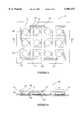
- circuit array 10manufactured according to the present invention is shown and generally designated 10.
- the circuit array 10is shown following encapsulation but prior to singulation.
- Circuit array 10is comprised of twelve individual circuits 12. However, a particular array can have a fewer or greater number of circuits 12.
- the circuit array 10includes a substrate 14.
- the substrate 14can be made of a number of materials which are known in the art. Preferably, to allow the finished product to remain flexible, the substrate 14 should be made of a flexible material such as polyester or PET. However, other suitable materials having the desired characteristics could be used as well. Furthermore, the substrate 14 is preferably very thin which can also contribute to its flexibility. By way of example and not limitation, the substrate 14 can be formed with a thickness of from 0.0009 inches (0.9 mils) to 0.010 inches (10 mil).
- Each circuit 12includes a conductive trace 16 formed on the substrate 14.
- the conductive trace 16can be formed as a single trace or as a pattern of conductive traces.
- the particular pattern or configuration of the conductive traces 16is not critical for the present invention. Instead, the pattern or configuration of the conductive trace 16 is dependent upon the type of circuit and the types and numbers of components to be used.
- the conductive traces 16can likewise be made of a number of materials and compositions, all of which are well known in the art.
- a conductive inkcan be applied to the substrate 14 using a conventional screen printing method.
- the conductive trace 16can be a patterned metal layer formed on substrate 14 using a conventional deposition, photopatterning and etching process.
- Attached to or mounted on the substrate 14are one or more electrical components.
- a battery 18 and a semiconductor die 20are mounted to the substrate 14.
- Other circuitry and circuit componentse.g., resistors, diodes, antennae
- these other circuit componentscan be separate members attached to the substrate 14 or can be integral components formed by screen printing or other deposition processes.
- the battery 18is a thin coin cell battery. Furthermore, in order to facilitate the mounting of the battery 18 onto the substrate, the battery 18 is preferably of a type having both the positive and the negative terminals on one side of the battery and substantially co-planar to one another.
- a suitable battery and contact assemblyis described in U.S. Pat. No. 5,558,679 entitled “Improved Battery and Contact Assembly and Method of Manufacture For Mounting A Battery.” The disclosure of that patent is hereby incorporated by reference.
- the battery 18 and the die 20are preferably mounted onto the substrate 14 using conductive adhesive such as a silver filled conductive epoxy or a z-axis anisotropic epoxy.
- the conductive adhesivealso establishes an electrical connection with the conductive trace 16.
- the battery 18is positioned on substrate 14 such that the positive terminal and the negative terminal of battery 18 make contact with appropriate portions of the conductive trace 16.
- the bond pads of die 20are placed such that they are in electrical contact with the appropriate portions of conductive trace 16. Constructed as such, the conductive trace 16, the battery 18 and the die 20 form the circuit 12.
- a barrieris formed for encapsulating the circuits 12.
- the barrieris a compartmental dam 22 that encloses each circuit 12 separately.
- the compartmental dam 22is preferably formed of a thin walled rigid material such as stainless steel or hard plastic.
- the compartmental dam 22includes an opening 24 for each separate circuit 12.
- the openings 24are shown having a substantially square configuration. However, other shapes such as polygonal, round or oval can also be used.
- the compartmental dam 22is placed in contact with the substrate 14 to prevent the encapsulating material from leaking out.
- the dam 22can be maintained in contact with the substrate under its own weight or by using a clamp or additional weight.
- the openings 24 and the substrate 14form a cavity 26 for each circuit 12.
- Each circuit 12is thus surrounded on four sides by the dam 22 and at the bottom by the substrate 14.
- the height of the dam 22is preferably sufficient such that the top surface 28 of the dam 22 is higher than the top of the highest circuit component.
- the top edge of the dam 22can also be contoured to conform to the surface topography of the circuit components.
- the encapsulant 30can be made from a variety of materials, any of which can be cured or dried from a viscous or liquid state to a hardened state.
- the encapsulant 30comprises a two-part epoxy and can include pigments or carbon to make the encapsulant opaque. In FIGS. 1 and 2 the encapsulant 30 is shown as transparent to allow viewing of the components.
- the particular formulations of the epoxyare a design consideration that are dependent on the desired curing times, curing methods, resulting hardness and resulting flexibility of the encapsulant 30. As those skilled in the art will appreciate, the particular formulation can be varied to achieve the particular characteristics desired.
- curingcan be effected in stages such that a partial cure can be performed to allow removal of the dam 22 followed by a total cure without the dam 22.
- the encapsulant 30does not need to completely fill the cavity for the present invention. In some situations it is desirable that the encapsulant 30 does not completely cover the components or is deposited with different thicknesses on different portions of the substrate.
- the circuit array 10can be singulated to separate the individual enclosed circuits 12.
- the singulation processcan be by routering or shearing or any other method known in the art without departing from the scope and spirit of the present invention.
- the singulation or separationcan result in the particular enclosed circuits having portions of the dam 22 remaining or completely trimmed away.
- a releasing agentcan be an anti-stick material, such as a mold release agent, that is applied to the dam prior to use or a permanently bonded material such as Teflon.
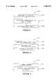
- FIGS. 3 and 4An alternate embodiment of the present invention is shown in FIGS. 3 and 4.
- the circuit array of enclosed circuitsis generally designated 40.
- circuit arraycomprises an array of twelve enclosed circuits 42.
- the alternate embodimentis substantially similar to the embodiment shown in FIGS. 1 and 2 except that a barrier for encapsulation is formed as a perimeter dam 54.
- the circuit array 40has as its foundation, a substrate 44.
- the substrate 44can be made of any of a number of materials, but is preferably made of a flexible polyester material or PET to allow the final product to remain flexible. Additionally, using a flexible polyester or PET allows the substrate to have a minimal thickness while maintaining sufficient strength.
- a conductive trace 46is formed on the substrate 44.
- the conductive trace 46can be formed as previously described.
- Mounted on the substrate 44are a variety of electrical components. As was the case in the prior embodiment, a battery 48 and a die 50 are mounted onto the substrate 44. Preferably, these components are attached to the substrate 44 and electrically connected to the conductive trace 46 using a conductive adhesive and preferably a silver filled epoxy adhesive as previously described.
- a portion of the trace 46is formed as an antenna 52.
- the antenna 52could also be formed as a separate component mounted onto the substrate.
- each circuit 42can communicate with the outside world using RF signals instead of requiring a hard-wired connection.
- information transmitted to the antenna 52can be stored within the die 50. The circuits 42 can thus be used to receive information, store information and transmit information.
- the perimeter dam 54is mounted or attached to the substrate 44 substantially as previously described.
- the perimeter dam 54is mounted onto substrate 44 such that it encompasses the periphery of the twelve enclosed circuits 42.
- the height of the perimeter dam 54is such that the top surface 56 of the dam 54 is higher than the tallest component utilized within the circuits 42.
- the perimeter dam 54in combination with the substrate 44, provides a single cavity 58 containing all twelve enclosed circuits 42.
- the cavity 58is filled with an encapsulant 60.
- the encapsulant 60can be made of any of a variety of materials (e.g., two part room temperature curing epoxy) which can be cured or hardened from a liquid state to a hardened state.
- the individual enclosed circuits 42can be singulated or separated from each other by cutting, routering or shearing or other methods known in the art. If desired, the perimeter dam 54 can be trimmed from the particular individual circuits 42 by similar methods. Additionally in order to facilitate separation of the perimeter dam 54 from the encapsulant 60 and the substrate 44, a releasing agent can be applied to the perimeter dam 54 prior to mounting the dam to the substrate 44 and prior to filling the cavity 58 with encapsulant 60. Preferably, sufficient encapsulant 60 is utilized to give each enclosed circuit 42 a substantially flat top surface. As can be seen, the resulting circuit is completely encapsulated between the encapsulant 60 and substrate 44. On the other hand, because of the flexible nature of the substrate as well as the encapsulant, some flexing can still be possible.
- FIGS. 5-6Still another enclosed circuit array according to the present invention is shown in FIGS. 5-6 and is generally designated 70.
- Circuit array 70 as shownincludes 12 individual enclosed circuits 72 prior to singulation.
- the alternate embodimentis substantially similar to the embodiment shown in FIGS. 1 and 2 except that a barrier for encapsulation is formed as a spacer sheet 84 having a cut out for each circuit 72.
- a substrate 74is included in the array 70.
- the substrate 74is flexible and substantially transparent.
- the substrate 74is made of polyester or PET and is approximately 0.9 mils (0.0009 in.) to 10 mils (0.010 in.) thick. Other materials and thicknesses can be used without departing from the scope and spirit of the present invention.
- An ink layer 75(FIG. 6) is applied to the substrate 74.
- the ink layer 75permits the formation of numbering, letter logos, graphic designs and the like on the inside surface of substrate 74.
- the ink layer 75can comprise multiple colors of ink and can be applied using known screen printing methods or other comparable methods. Because the lettering, numbers logos or graphic designs are to visible and viewed through the substrate 74, the images can be applied in a reversed orientation.
- a conductive trace 76, a battery 78 and a die 80are mounted onto substrate 74.
- the conductive trace 76is preferably formed as described above by screen printing or etching.
- the battery 78 and die 80are preferably attached to the substrate 44 using a conductive adhesive as previously described.
- a portion of the trace 76is formed as an antenna 82.
- the spacer sheet 84is preferably made of a flexible material like polycarbonate.
- the spacer sheet 84is formed with a plurality of openings 85 (or cutouts) having a shape that closely matches the peripheral shape of the circuits 72.
- the openings 85form a cavity 88 for encapsulating each circuit 72.
- the height or thickness of sheet 84is such that the top surface 86 of the sheet 84 is higher than the tallest component utilized within the circuit.
- the encapsulant 90is poured into the cavity 88 for each circuit 72.
- the encapsulant 90can be made of any of a variety of materials which can be cured or hardened from a liquid state to a hardened state.
- the individual enclosed circuits 72can be singulated or separated from each other by routering or shearing or other methods known in the art.
- portions of the spacer sheet 84become a permanent part of the enclosed circuit 72.
- sufficient encapsulant 90is utilized to give each enclosed circuit 72 a substantially flat top surface. As can be seen, the resulting circuit is completely encapsulated between the encapsulant 90, spacer sheet 84 and the substrate 74.
- each circuit 72will include the ink layer 75 visible through the substrate 74. Because the ink layer 75 is on the protected side of the substrate 74, it will have substantially improved wear characteristics. Additionally, the markings will be virtually tamper-proof and would be useful as an anti-counterfeiting measure.
- circuit array 100includes a substrate 104 on which a conductive trace 106 is formed. Mounted onto the substrate 104 is a battery 108 and a die 110. As before, a portion of the conductive trace 106 is formed as an antenna 112. Still further, a perimeter dam 114 is attached to substrate 104, providing a cavity 116 which is filled by an encapsulant 118. In the view shown in FIG. 7, four enclosed circuits 102 are shown.
- an additional flexible cover 120is attached to the top surface of the perimeter dam 114 and the encapsulant 118.
- the flexible cover 120can be attached while the encapsulant is still in its liquid state or can be attached to the encapsulant with an adhesive or other suitable bonding means after the encapsulant 118 has hardened. While cover 120 is shown on a circuit array similar to that shown in FIGS. 3-4, it could be used on other similar circuits or circuit arrays like that shown in FIGS. 1-2 or FIGS. 5-6. Additionally while the flexible cover 120 is preferably a flexible material such as polyester or PET, some instances may require additional strength, and harder and less flexible materials may be used.
- Circuit 130is shown in its completed state post-singulation.
- the substrate 132is preferably made of materials as previously described.
- a conductive trace 134is formed on the substrate 132.
- Mounted on the substrate 132 in electrical communication with the conductive trace 134are a battery 136 and a die 138.
- Also mounted to the substrate 132is a barrier 140.
- the battery 136 and die 138are within the cavity formed by substrate 132 and barrier 140. Filling the remainder of the cavity is an encapsulant 142.
- the contact trace 134extends out beyond the periphery of the barrier 140. In this manner a portion of contact trace 134 is on the outside of the circuit 130 and forms an edge connector 144 similar to standard circuit board connectors which will be recognized by those skilled in the art. Edge connector 144 could be connected to other circuits and components by physical contact or soldering or by other means known in the art. Enclosed circuit 130 could thus be used in a hard-wired assembly.
- a flowchart for the preferred method of manufactureis shown in broad steps in FIG. 9 and is generally designated 210.
- a substrateis initially formed or provided, step 212.
- the substratecan be made of a number of materials, although it is preferably flexible and, for the preferred embodiment, is normally material like polyester or PET.
- step 212the components of the circuit are mounted onto the substrate, step 214, such that a circuit is formed on the substrate. More specifically, for a typical circuit, the mounting components substep 214 is shown in FIG. 10. As shown in FIG. 10, a conductive trace is formed on the substrate, step 216. The conductive trace can be formed on the substrate using a variety of methods, including screen printing, etching and others that are known in the art.
- a conductive adhesiveis applied to the top surface of the substrate and the conductive trace.
- the adhesiveis a conductive adhesive. In the preferred configuration, this adhesive is applied in a layer approximately 2 mil. thick.
- the electrical components of the circuitrycan then be applied and mounted onto the substrate and are held in place by the adhesive.
- a diecan be placed onto the substrate, step 218.
- the dieis positioned such that its electrical contacts (e.g., bond pads) are immediately adjacent the appropriate locations on the conductive trace. In this manner, utilizing a conductive adhesive, electrical communication is established between the die and conductive trace.
- a batterycan be mounted onto the substrate and also held in place by the adhesive, step 220. Both the positive and negative terminals of this battery are placed immediately adjacent the positive and negative contact trace of the conductive trace. In this manner, a circuit is formed between the battery, the die and the conductive trace.
- an additional conductive adhesivecan be applied around the perimeter of the battery to provide additional electrical contact. This may be necessary where the positive and negative terminals of the batter are not coplanar.
- the final step in the methodis to encapsulate the circuit, step 222.
- the substep of encapsulating the circuit, step 222,is shown in FIG. 11.
- a barrier to contain the encapsulantmust be formed.
- the barriercan be either a compartmentalized dam or spacer sheet having a number of openings or cut outs, one for each enclosed circuit, or a perimeter dam having a single opening surrounding a number of enclosed circuits.
- the individual dam or spacer sheetcan be manufactured by a variety of methods.
- an initial piece of stock of, for example, black polycarbonateis provided.
- This sheetis then cut to size for the overall dimensions of the individual dam.
- the individual openingse.g., 24 or 85
- the sheetcan be initially formed with openings (e.g., 24 or 85) such as by molding without departing from the scope of the present invention.
- Openingscan have a standardized shape as is shown for openings 24 or could be designed to conform to the shape of the componentry like opening 85.
- mounting the barrier onto the substrateis step 224.
- the barrieritself may be held in contact with the substrate using an adhesive or by bonding or by other means known in the art.
- a releasing agentcan be applied to the barrier.
- the barriercould be applied to the substrate using a releasing agent, or be held in place using other non-permanent means like pressure, a magnetic field, and the like to allow the barrier to be reused.
- the cavitywhich contains the circuit components, is substantially filled with an encapsulant, step 226.
- the encapsulantis then allowed to dry or is cured. Once the encapsulant has hardened, the individual enclosed circuits can be singulated by routering or shearing or other means known in the art. If desired, the remaining portions of the barrier can be removed for reuse, trimmed away or can be left in contact with the individual enclosed circuits.
- markingse.g. lettering, numbering, logos or graphic representations on the enclosed circuit.
- markingse.g. lettering, numbering, logos or graphic representations
- a substratethat is substantially transparent.
- an ink layeris applied to the surface of the substrate by screen printing or other similar means. If multiple colors are desired, multiple layers can be applied. In order to be visible through the substrate, the images are applied in reverse orientation as will be appreciated by those skilled in the art.
- the tracecan be formed such that it extends out beyond the barrier to form an edge connector.
- the extension of the substrate including the edge connectoris allowed to remain.
- an additional covercan be added to the top of the barrier and the encapsulant prior to singulation.
- This covercan be a variety of materials, including flexible polyester or PET. It can be attached to the encapsulant while the encapsulant is still in its liquid state or it can be attached after the encapsulant has hardened using an adhesive or bonding or other means known in the art.
- the inventionprovides an improved enclosed electrical circuit using an encapsulant. Furthermore, although the method of the invention has been described with reference to certain preferred embodiments and preferred methods, as will be apparent to those skilled in the art, certain changes and modifications can be made without departing from the scope of the invention as defined by the following claims.
Landscapes
- Engineering & Computer Science (AREA)
- Microelectronics & Electronic Packaging (AREA)
- Power Engineering (AREA)
- Computer Hardware Design (AREA)
- Physics & Mathematics (AREA)
- Condensed Matter Physics & Semiconductors (AREA)
- General Physics & Mathematics (AREA)
- Manufacturing & Machinery (AREA)
- Chemical & Material Sciences (AREA)
- Dispersion Chemistry (AREA)
- Non-Metallic Protective Coatings For Printed Circuits (AREA)
- Structures Or Materials For Encapsulating Or Coating Semiconductor Devices Or Solid State Devices (AREA)
Abstract
Description
Claims (11)
Priority Applications (1)
| Application Number | Priority Date | Filing Date | Title |
|---|---|---|---|
| US08/814,206US5907477A (en) | 1995-09-19 | 1997-03-11 | Substrate assembly including a compartmental dam for use in the manufacturing of an enclosed electrical circuit using an encapsulant |
Applications Claiming Priority (2)
| Application Number | Priority Date | Filing Date | Title |
|---|---|---|---|
| US08/530,747US5612513A (en) | 1995-09-19 | 1995-09-19 | Article and method of manufacturing an enclosed electrical circuit using an encapsulant |
| US08/814,206US5907477A (en) | 1995-09-19 | 1997-03-11 | Substrate assembly including a compartmental dam for use in the manufacturing of an enclosed electrical circuit using an encapsulant |
Related Parent Applications (1)
| Application Number | Title | Priority Date | Filing Date |
|---|---|---|---|
| US08/530,747ContinuationUS5612513A (en) | 1995-09-19 | 1995-09-19 | Article and method of manufacturing an enclosed electrical circuit using an encapsulant |
Publications (1)
| Publication Number | Publication Date |
|---|---|
| US5907477Atrue US5907477A (en) | 1999-05-25 |
Family
ID=24114794
Family Applications (2)
| Application Number | Title | Priority Date | Filing Date |
|---|---|---|---|
| US08/530,747Expired - LifetimeUS5612513A (en) | 1995-09-19 | 1995-09-19 | Article and method of manufacturing an enclosed electrical circuit using an encapsulant |
| US08/814,206Expired - LifetimeUS5907477A (en) | 1995-09-19 | 1997-03-11 | Substrate assembly including a compartmental dam for use in the manufacturing of an enclosed electrical circuit using an encapsulant |
Family Applications Before (1)
| Application Number | Title | Priority Date | Filing Date |
|---|---|---|---|
| US08/530,747Expired - LifetimeUS5612513A (en) | 1995-09-19 | 1995-09-19 | Article and method of manufacturing an enclosed electrical circuit using an encapsulant |
Country Status (1)
| Country | Link |
|---|---|
| US (2) | US5612513A (en) |
Cited By (151)
| Publication number | Priority date | Publication date | Assignee | Title |
|---|---|---|---|---|
| WO1999047332A1 (en)* | 1998-03-17 | 1999-09-23 | Cardxx, Inc. | Method for making smart cards using isotropic thermoset adhesive materials |
| US6067025A (en)* | 1997-12-03 | 2000-05-23 | Stmicroelectronics, Inc. | Apparatus and method for detecting the height above a silicon surface |
| US6085324A (en)* | 1997-02-05 | 2000-07-04 | Ogram; Mark E. | Monitoring and regulatory system for the internet |
| US6131269A (en)* | 1998-05-18 | 2000-10-17 | Trw Inc. | Circuit isolation technique for RF and millimeter-wave modules |
| US6246010B1 (en)* | 1998-11-25 | 2001-06-12 | 3M Innovative Properties Company | High density electronic package |
| US6243945B1 (en)* | 1998-07-02 | 2001-06-12 | Murata Manufacturing Co., Ltd. | Method for manufacturing electronic parts |
| EP1162661A1 (en)* | 2000-06-06 | 2001-12-12 | STMicroelectronics S.r.l. | Electronic semiconductor device having a heat spreader |
| US6356453B1 (en)* | 2000-06-29 | 2002-03-12 | Amkor Technology, Inc. | Electronic package having flip chip integrated circuit and passive chip component |
| WO2002031881A1 (en)* | 2000-10-13 | 2002-04-18 | Tyco Electronics Amp Gmbh | Electronic unit and process for the production thereof |
| US20020098623A1 (en)* | 2000-08-31 | 2002-07-25 | Salman Akram | Semiconductor device including leads in communication with contact pads thereof and a stereolithographically fabricated package substantially encapsulating the leads and methods for fabricating the same |
| US6445589B2 (en)* | 1999-07-29 | 2002-09-03 | Delphi Technologies, Inc. | Method of extending life expectancy of surface mount components |
| US20020130817A1 (en)* | 2001-03-16 | 2002-09-19 | Forster Ian J. | Communicating with stackable objects using an antenna array |
| US20030030122A1 (en)* | 1996-11-12 | 2003-02-13 | Salman Akram | Method for sawing wafers employing multiple indexing techniques for multiple die dimensions |
| US6521484B1 (en)* | 1997-01-08 | 2003-02-18 | Orient Semiconductor Electronics, Ltd. | Mold injection method for semiconductor device |
| US6546620B1 (en) | 2000-06-29 | 2003-04-15 | Amkor Technology, Inc. | Flip chip integrated circuit and passive chip component package fabrication method |
| FR2831327A1 (en)* | 2001-10-22 | 2003-04-25 | Commissariat Energie Atomique | Microelectronic or nanoelectronic component incorporating energy sources in a sealed protective cavity in a substrate |
| US20030181846A1 (en)* | 2001-12-19 | 2003-09-25 | Young Wendy A. | Reservoir housing having a conductive region integrally formed therein |
| US6627997B1 (en)* | 1999-03-26 | 2003-09-30 | Hitachi, Ltd. | Semiconductor module and method of mounting |
| EP1120823A3 (en)* | 2000-01-28 | 2004-01-02 | NEC Compound Semiconductor Devices, Ltd. | Semiconductor device substrate and method of manufacturing semiconductor device |
| US20040036657A1 (en)* | 2002-04-24 | 2004-02-26 | Forster Ian J. | Energy source communication employing slot antenna |
| US6713878B2 (en)* | 2001-05-30 | 2004-03-30 | Stmicroelectronics | Electronic element with a shielding |
| US20040080299A1 (en)* | 2002-04-24 | 2004-04-29 | Forster Ian J. | Energy source recharging device and method |
| US20040106376A1 (en)* | 2002-04-24 | 2004-06-03 | Forster Ian J. | Rechargeable interrogation reader device and method |
| EP1143508A3 (en)* | 2000-03-23 | 2004-06-23 | Infineon Technologies AG | Apparatus for packaging electronic components |
| US20040129786A1 (en)* | 2001-02-02 | 2004-07-08 | Yves Reignoux | Portable object with chip and antenna |
| US6784844B1 (en)* | 1999-10-08 | 2004-08-31 | Nokia Mobile Phone Limited | Antenna assembly and method of construction |
| US6784541B2 (en) | 2000-01-27 | 2004-08-31 | Hitachi, Ltd. | Semiconductor module and mounting method for same |
| US20040188123A1 (en)* | 2003-03-18 | 2004-09-30 | Peterson Darin L. | Microelectronic component assemblies having exposed contacts |
| US20040191963A1 (en)* | 2003-03-31 | 2004-09-30 | Osram Opto Semiconductors Gmbh | Encapsulation of thin-film electronic devices |
| US20050074922A1 (en)* | 2003-10-01 | 2005-04-07 | Lintec Corporation | Process for producing resin-sealed type electronic device |
| US6886244B1 (en)* | 2002-02-25 | 2005-05-03 | Seagate Technology Llc | Segmented pallet for disk-shaped substrate electrical biassing and apparatus comprising same |
| US6949822B2 (en)* | 2000-03-17 | 2005-09-27 | International Rectifier Corporation | Semiconductor multichip module package with improved thermal performance; reduced size and improved moisture resistance |
| US20050283794A1 (en)* | 2004-06-22 | 2005-12-22 | Samsung Electronics Co., Ltd. | Anti-hacking printed circuit board having high-molecular material deposited thereon and deposition method for the same |
| US20060010685A1 (en)* | 2004-07-15 | 2006-01-19 | Fujitsu Limited | RFID tag and method of manufacturing RFID tag |
| US20060258050A1 (en)* | 2004-03-30 | 2006-11-16 | Joji Fujiwara | Module component and method for manufacturing the same |
| US20060281227A1 (en)* | 2005-06-14 | 2006-12-14 | Miradia Inc. | Bond method and structure using selective application of spin on glass |
| US20070018297A1 (en)* | 2005-07-25 | 2007-01-25 | Kingston Technology Company, Inc. | High-capacity memory card and method of making the same |
| GB2439837A (en)* | 2006-07-05 | 2008-01-09 | Yuejun Yan | Method for packaging an electronic component using resin |
| US20080055863A1 (en)* | 2006-09-05 | 2008-03-06 | Samsung Electro-Mechanics Co., Ltd. | Method of manufacturing as component embedded printed circuit board |
| US20080086867A1 (en)* | 2006-10-17 | 2008-04-17 | Kerr Geoffrey H | Circuit component locating apparatus |
| EP1937039A1 (en)* | 2006-12-18 | 2008-06-25 | Albea Kunstofftechnik GmbH | Membrane structure with at least one antenna |
| WO2009000636A1 (en)* | 2007-06-26 | 2008-12-31 | Nagraid S.A. | Method for manufacturing boards including at least one electronic module, assembly used in said method and intermediate product |
| US7548430B1 (en)* | 2002-05-01 | 2009-06-16 | Amkor Technology, Inc. | Buildup dielectric and metallization process and semiconductor package |
| US7550857B1 (en) | 2006-11-16 | 2009-06-23 | Amkor Technology, Inc. | Stacked redistribution layer (RDL) die assembly package |
| US7629674B1 (en) | 2004-11-17 | 2009-12-08 | Amkor Technology, Inc. | Shielded package having shield fence |
| US7633765B1 (en) | 2004-03-23 | 2009-12-15 | Amkor Technology, Inc. | Semiconductor package including a top-surface metal layer for implementing circuit features |
| US7671457B1 (en) | 2002-05-01 | 2010-03-02 | Amkor Technology, Inc. | Semiconductor package including top-surface terminals for mounting another semiconductor package |
| US20100073255A1 (en)* | 2008-09-25 | 2010-03-25 | Skyworks Solutions, Inc. | Overmolded semiconductor package with an integrated antenna |
| US20100127371A1 (en)* | 2008-11-26 | 2010-05-27 | Infineon Technologies Ag | Power semiconductor module with segmented base plate |
| US20100136413A1 (en)* | 2008-12-02 | 2010-06-03 | Tesla Motors, Inc. | Method and apparatus for the external application of battery pack encapsulant |
| US7851894B1 (en) | 2008-12-23 | 2010-12-14 | Amkor Technology, Inc. | System and method for shielding of package on package (PoP) assemblies |
| US20110019370A1 (en)* | 2009-07-27 | 2011-01-27 | Gainteam Holdings Limited | Flexible circuit module |
| US7898066B1 (en) | 2007-05-25 | 2011-03-01 | Amkor Technology, Inc. | Semiconductor device having EMI shielding and method therefor |
| US7915715B2 (en) | 2008-11-25 | 2011-03-29 | Amkor Technology, Inc. | System and method to provide RF shielding for a MEMS microphone package |
| EP2320356A1 (en)* | 2009-10-27 | 2011-05-11 | Giesecke & Devrient GmbH | Method for manufacturing inlays for card-shaped data carriers |
| US20110128712A1 (en)* | 2009-12-01 | 2011-06-02 | Prest Christopher D | Compact media player |
| US7960827B1 (en) | 2009-04-09 | 2011-06-14 | Amkor Technology, Inc. | Thermal via heat spreader package and method |
| US20110204497A1 (en)* | 2010-02-24 | 2011-08-25 | Renesas Electronics Corporation | Semiconductor integrated circuit and method for manufacturing the same |
| US8012868B1 (en) | 2008-12-15 | 2011-09-06 | Amkor Technology Inc | Semiconductor device having EMI shielding and method therefor |
| US8102032B1 (en) | 2008-12-09 | 2012-01-24 | Amkor Technology, Inc. | System and method for compartmental shielding of stacked packages |
| US8129824B1 (en) | 2008-12-03 | 2012-03-06 | Amkor Technology, Inc. | Shielding for a semiconductor package |
| US8199518B1 (en) | 2010-02-18 | 2012-06-12 | Amkor Technology, Inc. | Top feature package and method |
| US8222538B1 (en) | 2009-06-12 | 2012-07-17 | Amkor Technology, Inc. | Stackable via package and method |
| US8294276B1 (en) | 2010-05-27 | 2012-10-23 | Amkor Technology, Inc. | Semiconductor device and fabricating method thereof |
| US8300423B1 (en) | 2010-05-25 | 2012-10-30 | Amkor Technology, Inc. | Stackable treated via package and method |
| US8337657B1 (en) | 2010-10-27 | 2012-12-25 | Amkor Technology, Inc. | Mechanical tape separation package and method |
| US8338229B1 (en) | 2010-07-30 | 2012-12-25 | Amkor Technology, Inc. | Stackable plasma cleaned via package and method |
| US8471154B1 (en) | 2009-08-06 | 2013-06-25 | Amkor Technology, Inc. | Stackable variable height via package and method |
| US20130163210A1 (en)* | 2011-12-27 | 2013-06-27 | Apple Inc. | Integrated flex tail circuit packaging |
| US8482134B1 (en) | 2010-11-01 | 2013-07-09 | Amkor Technology, Inc. | Stackable package and method |
| US8508023B1 (en) | 2010-06-17 | 2013-08-13 | Amkor Technology, Inc. | System and method for lowering contact resistance of the radio frequency (RF) shield to ground |
| US8525318B1 (en) | 2010-11-10 | 2013-09-03 | Amkor Technology, Inc. | Semiconductor device and fabricating method thereof |
| US8536462B1 (en) | 2010-01-22 | 2013-09-17 | Amkor Technology, Inc. | Flex circuit package and method |
| US8535961B1 (en) | 2010-12-09 | 2013-09-17 | Amkor Technology, Inc. | Light emitting diode (LED) package and method |
| US8557629B1 (en) | 2010-12-03 | 2013-10-15 | Amkor Technology, Inc. | Semiconductor device having overlapped via apertures |
| US8623753B1 (en) | 2009-05-28 | 2014-01-07 | Amkor Technology, Inc. | Stackable protruding via package and method |
| US8633598B1 (en) | 2011-09-20 | 2014-01-21 | Amkor Technology, Inc. | Underfill contacting stacking balls package fabrication method and structure |
| US8653674B1 (en) | 2011-09-15 | 2014-02-18 | Amkor Technology, Inc. | Electronic component package fabrication method and structure |
| US8698323B2 (en)* | 2012-06-18 | 2014-04-15 | Invensas Corporation | Microelectronic assembly tolerant to misplacement of microelectronic elements therein |
| US8717775B1 (en) | 2010-08-02 | 2014-05-06 | Amkor Technology, Inc. | Fingerprint sensor package and method |
| US8796561B1 (en) | 2009-10-05 | 2014-08-05 | Amkor Technology, Inc. | Fan out build up substrate stackable package and method |
| US20140240175A1 (en)* | 2005-03-31 | 2014-08-28 | Semiconductor Energy Laboratory Co., Ltd. | Wireless chip and electronic device having wireless chip |
| US8890329B2 (en) | 2011-04-26 | 2014-11-18 | Amkor Technology, Inc. | Semiconductor device |
| US20150008566A1 (en)* | 2013-07-02 | 2015-01-08 | Texas Instruments Incorporated | Method and structure of panelized packaging of semiconductor devices |
| US8937381B1 (en) | 2009-12-03 | 2015-01-20 | Amkor Technology, Inc. | Thin stackable package and method |
| US8946886B1 (en) | 2010-05-13 | 2015-02-03 | Amkor Technology, Inc. | Shielded electronic component package and method |
| US9013011B1 (en) | 2011-03-11 | 2015-04-21 | Amkor Technology, Inc. | Stacked and staggered die MEMS package and method |
| US9029962B1 (en) | 2011-10-12 | 2015-05-12 | Amkor Technology, Inc. | Molded cavity substrate MEMS package fabrication method and structure |
| EP2924725A1 (en)* | 2014-03-25 | 2015-09-30 | ABB Technology Ltd | Electric module for subsea applications |
| US9159635B2 (en) | 2011-05-27 | 2015-10-13 | Mc10, Inc. | Flexible electronic structure |
| US9168094B2 (en) | 2012-07-05 | 2015-10-27 | Mc10, Inc. | Catheter device including flow sensing |
| US9171794B2 (en) | 2012-10-09 | 2015-10-27 | Mc10, Inc. | Embedding thin chips in polymer |
| US9186060B2 (en) | 2008-10-07 | 2015-11-17 | Mc10, Inc. | Systems, methods and devices having stretchable integrated circuitry for sensing and delivering therapy |
| US9226402B2 (en) | 2012-06-11 | 2015-12-29 | Mc10, Inc. | Strain isolation structures for stretchable electronics |
| WO2016003482A1 (en)* | 2014-07-01 | 2016-01-07 | Mc10, Inc. | Conformal electronic devices |
| US9289132B2 (en) | 2008-10-07 | 2016-03-22 | Mc10, Inc. | Catheter balloon having stretchable integrated circuitry and sensor array |
| US9295842B2 (en) | 2012-07-05 | 2016-03-29 | Mc10, Inc. | Catheter or guidewire device including flow sensing and use thereof |
| US9372123B2 (en) | 2013-08-05 | 2016-06-21 | Mc10, Inc. | Flexible temperature sensor including conformable electronics |
| US9391043B2 (en) | 2012-11-20 | 2016-07-12 | Amkor Technology, Inc. | Semiconductor device and manufacturing method thereof |
| US9516758B2 (en) | 2008-10-07 | 2016-12-06 | Mc10, Inc. | Extremely stretchable electronics |
| US9543242B1 (en) | 2013-01-29 | 2017-01-10 | Amkor Technology, Inc. | Semiconductor package and fabricating method thereof |
| US9545216B2 (en) | 2011-08-05 | 2017-01-17 | Mc10, Inc. | Catheter balloon methods and apparatus employing sensing elements |
| US9545285B2 (en) | 2011-10-05 | 2017-01-17 | Mc10, Inc. | Cardiac catheter employing conformal electronics for mapping |
| US9579040B2 (en) | 2011-09-01 | 2017-02-28 | Mc10, Inc. | Electronics for detection of a condition of tissue |
| USD781270S1 (en) | 2014-10-15 | 2017-03-14 | Mc10, Inc. | Electronic device having antenna |
| US9595509B1 (en)* | 2015-09-08 | 2017-03-14 | Nxp Usa, Inc. | Stacked microelectronic package assemblies and methods for the fabrication thereof |
| US9603287B1 (en)* | 2015-10-30 | 2017-03-21 | Industrial Technology Research Institute | Integrated power module |
| US9691635B1 (en) | 2002-05-01 | 2017-06-27 | Amkor Technology, Inc. | Buildup dielectric layer having metallization pattern semiconductor package fabrication method |
| US9691734B1 (en) | 2009-12-07 | 2017-06-27 | Amkor Technology, Inc. | Method of forming a plurality of electronic component packages |
| US9702839B2 (en) | 2011-03-11 | 2017-07-11 | Mc10, Inc. | Integrated devices to facilitate quantitative assays and diagnostics |
| US9704908B2 (en) | 2008-10-07 | 2017-07-11 | Mc10, Inc. | Methods and applications of non-planar imaging arrays |
| US9704842B2 (en) | 2013-11-04 | 2017-07-11 | Amkor Technology, Inc. | Interposer, manufacturing method thereof, semiconductor package using the same, and method for fabricating the semiconductor package |
| US9704747B2 (en) | 2013-03-29 | 2017-07-11 | Amkor Technology, Inc. | Semiconductor device and manufacturing method thereof |
| US9721872B1 (en) | 2011-02-18 | 2017-08-01 | Amkor Technology, Inc. | Methods and structures for increasing the allowable die size in TMV packages |
| US9723122B2 (en) | 2009-10-01 | 2017-08-01 | Mc10, Inc. | Protective cases with integrated electronics |
| US9748154B1 (en) | 2010-11-04 | 2017-08-29 | Amkor Technology, Inc. | Wafer level fan out semiconductor device and manufacturing method thereof |
| US9757050B2 (en) | 2011-08-05 | 2017-09-12 | Mc10, Inc. | Catheter balloon employing force sensing elements |
| US9810623B2 (en) | 2014-03-12 | 2017-11-07 | Mc10, Inc. | Quantification of a change in assay |
| US9846829B2 (en) | 2012-10-09 | 2017-12-19 | Mc10, Inc. | Conformal electronics integrated with apparel |
| US20180040568A1 (en)* | 2016-08-05 | 2018-02-08 | Siliconware Precision Industries Co., Ltd. | Electronic package and method for fabricating the same |
| US9899330B2 (en) | 2014-10-03 | 2018-02-20 | Mc10, Inc. | Flexible electronic circuits with embedded integrated circuit die |
| US9929072B2 (en) | 2013-07-02 | 2018-03-27 | Texas Instruments Incorporated | Packaged semiconductor devices |
| US9949691B2 (en) | 2013-11-22 | 2018-04-24 | Mc10, Inc. | Conformal sensor systems for sensing and analysis of cardiac activity |
| US9960328B2 (en) | 2016-09-06 | 2018-05-01 | Amkor Technology, Inc. | Semiconductor device and manufacturing method thereof |
| US10001611B2 (en)* | 2016-03-04 | 2018-06-19 | Inphi Corporation | Optical transceiver by FOWLP and DoP multichip integration |
| US10083911B2 (en) | 2017-02-08 | 2018-09-25 | Advanced Semiconductor Engineering, Inc. | Semiconductor device package and method of manufacturing the same |
| US10177095B2 (en) | 2017-03-24 | 2019-01-08 | Amkor Technology, Inc. | Semiconductor device and method of manufacturing thereof |
| US10277386B2 (en) | 2016-02-22 | 2019-04-30 | Mc10, Inc. | System, devices, and method for on-body data and power transmission |
| US10297572B2 (en) | 2014-10-06 | 2019-05-21 | Mc10, Inc. | Discrete flexible interconnects for modules of integrated circuits |
| US10300371B2 (en) | 2015-10-01 | 2019-05-28 | Mc10, Inc. | Method and system for interacting with a virtual environment |
| US10334724B2 (en) | 2013-05-14 | 2019-06-25 | Mc10, Inc. | Conformal electronics including nested serpentine interconnects |
| US10398343B2 (en) | 2015-03-02 | 2019-09-03 | Mc10, Inc. | Perspiration sensor |
| US10410962B2 (en) | 2014-01-06 | 2019-09-10 | Mc10, Inc. | Encapsulated conformal electronic systems and devices, and methods of making and using the same |
| US20190310687A1 (en)* | 2018-04-05 | 2019-10-10 | Samsung Electro-Mechanics Co., Ltd. | Electronic device module and method of manufacturing the same |
| US10447347B2 (en) | 2016-08-12 | 2019-10-15 | Mc10, Inc. | Wireless charger and high speed data off-loader |
| US20190324223A1 (en)* | 2016-12-29 | 2019-10-24 | Intel Corporation | Photonic engine platform utilizing embedded wafer level packaging integration |
| US10467926B2 (en) | 2013-10-07 | 2019-11-05 | Mc10, Inc. | Conformal sensor systems for sensing and analysis |
| US10477354B2 (en) | 2015-02-20 | 2019-11-12 | Mc10, Inc. | Automated detection and configuration of wearable devices based on on-body status, location, and/or orientation |
| US10485118B2 (en) | 2014-03-04 | 2019-11-19 | Mc10, Inc. | Multi-part flexible encapsulation housing for electronic devices and methods of making the same |
| US10497650B2 (en) | 2017-04-13 | 2019-12-03 | Amkor Technology, Inc. | Semiconductor device and manufacturing method thereof |
| US10532211B2 (en) | 2015-10-05 | 2020-01-14 | Mc10, Inc. | Method and system for neuromodulation and stimulation |
| US20200037437A1 (en)* | 2018-07-24 | 2020-01-30 | Samsung Electro-Mechanics Co., Ltd. | Electronic device module |
| US20200050912A1 (en)* | 2016-10-17 | 2020-02-13 | Parkside Flexibles (Europe) Limited | Electronic identifier for packaging |
| US10653332B2 (en) | 2015-07-17 | 2020-05-19 | Mc10, Inc. | Conductive stiffener, method of making a conductive stiffener, and conductive adhesive and encapsulation layers |
| US10673280B2 (en) | 2016-02-22 | 2020-06-02 | Mc10, Inc. | System, device, and method for coupled hub and sensor node on-body acquisition of sensor information |
| US10709384B2 (en) | 2015-08-19 | 2020-07-14 | Mc10, Inc. | Wearable heat flux devices and methods of use |
| US10811277B2 (en) | 2004-03-23 | 2020-10-20 | Amkor Technology, Inc. | Encapsulated semiconductor package |
| US10879144B2 (en) | 2018-08-14 | 2020-12-29 | Texas Instruments Incorporated | Semiconductor package with multilayer mold |
| US11034068B2 (en) | 2018-04-30 | 2021-06-15 | Raytheon Company | Encapsulating electronics in high-performance thermoplastics |
| US11081370B2 (en) | 2004-03-23 | 2021-08-03 | Amkor Technology Singapore Holding Pte. Ltd. | Methods of manufacturing an encapsulated semiconductor device |
| US11154235B2 (en) | 2016-04-19 | 2021-10-26 | Medidata Solutions, Inc. | Method and system for measuring perspiration |
Families Citing this family (46)
| Publication number | Priority date | Publication date | Assignee | Title |
|---|---|---|---|---|
| US5776278A (en)* | 1992-06-17 | 1998-07-07 | Micron Communications, Inc. | Method of manufacturing an enclosed transceiver |
| USRE42773E1 (en) | 1992-06-17 | 2011-10-04 | Round Rock Research, Llc | Method of manufacturing an enclosed transceiver |
| US7158031B2 (en)* | 1992-08-12 | 2007-01-02 | Micron Technology, Inc. | Thin, flexible, RFID label and system for use |
| US6465743B1 (en)* | 1994-12-05 | 2002-10-15 | Motorola, Inc. | Multi-strand substrate for ball-grid array assemblies and method |
| JP3337847B2 (en)* | 1995-02-27 | 2002-10-28 | 株式会社東芝 | Manufacturing method of electronic component built-in card |
| US5612513A (en)* | 1995-09-19 | 1997-03-18 | Micron Communications, Inc. | Article and method of manufacturing an enclosed electrical circuit using an encapsulant |
| US5776798A (en) | 1996-09-04 | 1998-07-07 | Motorola, Inc. | Semiconductor package and method thereof |
| US6962829B2 (en)* | 1996-10-31 | 2005-11-08 | Amkor Technology, Inc. | Method of making near chip size integrated circuit package |
| US5981314A (en)* | 1996-10-31 | 1999-11-09 | Amkor Technology, Inc. | Near chip size integrated circuit package |
| US6150193A (en)* | 1996-10-31 | 2000-11-21 | Amkor Technology, Inc. | RF shielded device |
| US5815372A (en)* | 1997-03-25 | 1998-09-29 | Intel Corporation | Packaging multiple dies on a ball grid array substrate |
| JPH10284525A (en)* | 1997-04-03 | 1998-10-23 | Shinko Electric Ind Co Ltd | Method for producing semiconductor device |
| US6339385B1 (en) | 1997-08-20 | 2002-01-15 | Micron Technology, Inc. | Electronic communication devices, methods of forming electrical communication devices, and communication methods |
| US5962810A (en)* | 1997-09-09 | 1999-10-05 | Amkor Technology, Inc. | Integrated circuit package employing a transparent encapsulant |
| US6049094A (en)* | 1998-05-21 | 2000-04-11 | National Semiconductor Corporation | Low stress package assembly for silicon-backed light valves |
| US6251211B1 (en) | 1998-07-22 | 2001-06-26 | Micron Technology, Inc. | Circuitry interconnection method |
| US6569710B1 (en)* | 1998-12-03 | 2003-05-27 | International Business Machines Corporation | Panel structure with plurality of chip compartments for providing high volume of chip modules |
| JP2001024312A (en)* | 1999-07-13 | 2001-01-26 | Taiyo Yuden Co Ltd | Manufacture of electronic device, the electronic device, and method for filling resin |
| US6273339B1 (en) | 1999-08-30 | 2001-08-14 | Micron Technology, Inc. | Tamper resistant smart card and method of protecting data in a smart card |
| US6147662A (en)* | 1999-09-10 | 2000-11-14 | Moore North America, Inc. | Radio frequency identification tags and labels |
| US6656765B1 (en) | 2000-02-02 | 2003-12-02 | Amkor Technology, Inc. | Fabricating very thin chip size semiconductor packages |
| US6876052B1 (en)* | 2000-05-12 | 2005-04-05 | National Semiconductor Corporation | Package-ready light-sensitive integrated circuit and method for its preparation |
| US6624005B1 (en) | 2000-09-06 | 2003-09-23 | Amkor Technology, Inc. | Semiconductor memory cards and method of making same |
| US6951596B2 (en)* | 2002-01-18 | 2005-10-04 | Avery Dennison Corporation | RFID label technique |
| US6512482B1 (en)* | 2001-03-20 | 2003-01-28 | Xilinx, Inc. | Method and apparatus using a semiconductor die integrated antenna structure |
| US7566587B2 (en)* | 2001-12-03 | 2009-07-28 | Azimuth Industrial Co., Inc. | Method and apparatus for packaging electronic components |
| US6660562B2 (en)* | 2001-12-03 | 2003-12-09 | Azimuth Industrial Co., Inc. | Method and apparatus for a lead-frame air-cavity package |
| JP4103653B2 (en)* | 2003-03-27 | 2008-06-18 | 株式会社デンソー | IC card |
| US7266869B2 (en)* | 2003-07-30 | 2007-09-11 | Kyocera Corporation | Method for manufacturing a piezoelectric oscillator |
| TWI228304B (en)* | 2003-10-29 | 2005-02-21 | Advanced Semiconductor Eng | Method for manufacturing ball grid package |
| US7500307B2 (en)* | 2004-09-22 | 2009-03-10 | Avery Dennison Corporation | High-speed RFID circuit placement method |
| US7623034B2 (en)* | 2005-04-25 | 2009-11-24 | Avery Dennison Corporation | High-speed RFID circuit placement method and device |
| US7555826B2 (en)* | 2005-12-22 | 2009-07-07 | Avery Dennison Corporation | Method of manufacturing RFID devices |
| KR101271225B1 (en)* | 2006-10-31 | 2013-06-03 | 삼성디스플레이 주식회사 | Method for manufacturing light emitting diode chip and light emitting diode light source module |
| US20080160173A1 (en)* | 2006-12-27 | 2008-07-03 | Nokia Corporation | Component Moulding Process |
| KR100834684B1 (en)* | 2007-02-12 | 2008-06-02 | 삼성전자주식회사 | Electronic circuit package |
| DE102007008487A1 (en)* | 2007-02-19 | 2008-08-21 | Smartrac Ip B.V. | Method and semifinished product for producing an inlay |
| JP5579982B2 (en)* | 2008-12-15 | 2014-08-27 | ピーエスフォー ルクスコ エスエイアールエル | Intermediate structure of semiconductor device and method of manufacturing intermediate structure |
| US8383457B2 (en) | 2010-09-03 | 2013-02-26 | Stats Chippac, Ltd. | Semiconductor device and method of forming interposer frame over semiconductor die to provide vertical interconnect |
| USRE48111E1 (en) | 2009-08-21 | 2020-07-21 | JCET Semiconductor (Shaoxing) Co. Ltd. | Semiconductor device and method of forming interposer frame over semiconductor die to provide vertical interconnect |
| JP5633480B2 (en)* | 2011-06-30 | 2014-12-03 | 豊田合成株式会社 | Method for manufacturing light emitting device |
| USD729808S1 (en)* | 2013-03-13 | 2015-05-19 | Nagrastar Llc | Smart card interface |
| USD780763S1 (en)* | 2015-03-20 | 2017-03-07 | Nagrastar Llc | Smart card interface |
| CN112563155A (en)* | 2019-09-26 | 2021-03-26 | 伟创力有限公司 | Method of forming exposed cavities in a molded electronic device |
| US11729915B1 (en)* | 2022-03-22 | 2023-08-15 | Tactotek Oy | Method for manufacturing a number of electrical nodes, electrical node module, electrical node, and multilayer structure |
| CN119833411A (en)* | 2024-12-12 | 2025-04-15 | 西安微电子技术研究所 | Detachable cofferdam and encapsulation method |
Citations (25)
| Publication number | Priority date | Publication date | Assignee | Title |
|---|---|---|---|---|
| US4218701A (en)* | 1978-07-24 | 1980-08-19 | Citizen Watch Co., Ltd. | Package for an integrated circuit having a container with support bars |
| US4502903A (en)* | 1982-01-20 | 1985-03-05 | Polaroid Corporation | Method of making lithium batteries with laminar anodes |
| US4621035A (en)* | 1982-01-20 | 1986-11-04 | Polaroid Corporation | Lithium batteries with laminar anodes |
| US4814943A (en)* | 1986-06-04 | 1989-03-21 | Oki Electric Industry Co., Ltd. | Printed circuit devices using thermoplastic resin cover plate |
| US4903169A (en)* | 1986-04-03 | 1990-02-20 | Matsushita Electric Industrial Co., Ltd. | Shielded high frequency apparatus having partitioned shield case, and method of manufacture thereof |
| US5018005A (en)* | 1989-12-27 | 1991-05-21 | Motorola Inc. | Thin, molded, surface mount electronic device |
| US5136365A (en)* | 1990-09-27 | 1992-08-04 | Motorola, Inc. | Anisotropic conductive adhesive and encapsulant material |
| US5295044A (en)* | 1991-09-26 | 1994-03-15 | Kabushiki Kaisah Toshiba | Semiconductor device |
| US5321240A (en)* | 1992-01-30 | 1994-06-14 | Mitsubishi Denki Kabushiki Kaisha | Non-contact IC card |
| US5327010A (en)* | 1989-09-09 | 1994-07-05 | Ryoden Kasei Co., Ltd. | IC card having adhesion-preventing sheets |
| US5336931A (en)* | 1993-09-03 | 1994-08-09 | Motorola, Inc. | Anchoring method for flow formed integrated circuit covers |
| US5350645A (en)* | 1993-06-21 | 1994-09-27 | Micron Semiconductor, Inc. | Polymer-lithium batteries and improved methods for manufacturing batteries |
| US5362652A (en)* | 1993-11-22 | 1994-11-08 | Nalco Chemical Company | Spectrophotometric detection of hydroperoxides in hydrocarbons |
| US5386342A (en)* | 1992-01-30 | 1995-01-31 | Lsi Logic Corporation | Rigid backplane formed from a moisture resistant insulative material used to protect a semiconductor device |
| US5389738A (en)* | 1992-05-04 | 1995-02-14 | Motorola, Inc. | Tamperproof arrangement for an integrated circuit device |
| US5416358A (en)* | 1992-09-17 | 1995-05-16 | Mitsubishi Denki Kabushiki Kaisha | IC card including frame with lateral hole for injecting encapsulating resin |
| US5422514A (en)* | 1993-05-11 | 1995-06-06 | Micromodule Systems, Inc. | Packaging and interconnect system for integrated circuits |
| US5477047A (en)* | 1992-10-23 | 1995-12-19 | Matsushita Electric Industrial Co., Ltd. | Direct-contact type image sensor device, an image sensor unit, and methods for producing the same |
| US5528222A (en)* | 1994-09-09 | 1996-06-18 | International Business Machines Corporation | Radio frequency circuit and memory in thin flexible package |
| US5536466A (en)* | 1992-04-27 | 1996-07-16 | Futaba Denshi Kogyo Kabushiki Kaisha | Process for manufacturing transparent conductive film wiring board |
| US5558679A (en)* | 1995-08-21 | 1996-09-24 | Micron Communications, Inc. | Method for mounting a battery on a substrate |
| US5605547A (en)* | 1995-03-27 | 1997-02-25 | Micron Technology, Inc. | Method and apparatus for mounting a component to a substrate using an anisotropic adhesive, a compressive cover film, and a conveyor |
| US5612513A (en)* | 1995-09-19 | 1997-03-18 | Micron Communications, Inc. | Article and method of manufacturing an enclosed electrical circuit using an encapsulant |
| US5646828A (en)* | 1995-02-24 | 1997-07-08 | Lucent Technologies Inc. | Thin packaging of multi-chip modules with enhanced thermal/power management |
| US5866441A (en)* | 1994-12-22 | 1999-02-02 | Pace; Benedict G. | Inverted chip bonded module with high packaging efficiency |
- 1995
- 1995-09-19USUS08/530,747patent/US5612513A/ennot_activeExpired - Lifetime
- 1997
- 1997-03-11USUS08/814,206patent/US5907477A/ennot_activeExpired - Lifetime
Patent Citations (26)
| Publication number | Priority date | Publication date | Assignee | Title |
|---|---|---|---|---|
| US4218701A (en)* | 1978-07-24 | 1980-08-19 | Citizen Watch Co., Ltd. | Package for an integrated circuit having a container with support bars |
| US4502903A (en)* | 1982-01-20 | 1985-03-05 | Polaroid Corporation | Method of making lithium batteries with laminar anodes |
| US4621035A (en)* | 1982-01-20 | 1986-11-04 | Polaroid Corporation | Lithium batteries with laminar anodes |
| US4903169A (en)* | 1986-04-03 | 1990-02-20 | Matsushita Electric Industrial Co., Ltd. | Shielded high frequency apparatus having partitioned shield case, and method of manufacture thereof |
| US4814943A (en)* | 1986-06-04 | 1989-03-21 | Oki Electric Industry Co., Ltd. | Printed circuit devices using thermoplastic resin cover plate |
| US5327010A (en)* | 1989-09-09 | 1994-07-05 | Ryoden Kasei Co., Ltd. | IC card having adhesion-preventing sheets |
| US5018005A (en)* | 1989-12-27 | 1991-05-21 | Motorola Inc. | Thin, molded, surface mount electronic device |
| US5136365A (en)* | 1990-09-27 | 1992-08-04 | Motorola, Inc. | Anisotropic conductive adhesive and encapsulant material |
| US5295044A (en)* | 1991-09-26 | 1994-03-15 | Kabushiki Kaisah Toshiba | Semiconductor device |
| US5386342A (en)* | 1992-01-30 | 1995-01-31 | Lsi Logic Corporation | Rigid backplane formed from a moisture resistant insulative material used to protect a semiconductor device |
| US5321240A (en)* | 1992-01-30 | 1994-06-14 | Mitsubishi Denki Kabushiki Kaisha | Non-contact IC card |
| US5536466A (en)* | 1992-04-27 | 1996-07-16 | Futaba Denshi Kogyo Kabushiki Kaisha | Process for manufacturing transparent conductive film wiring board |
| US5389738A (en)* | 1992-05-04 | 1995-02-14 | Motorola, Inc. | Tamperproof arrangement for an integrated circuit device |
| US5416358A (en)* | 1992-09-17 | 1995-05-16 | Mitsubishi Denki Kabushiki Kaisha | IC card including frame with lateral hole for injecting encapsulating resin |
| US5477047A (en)* | 1992-10-23 | 1995-12-19 | Matsushita Electric Industrial Co., Ltd. | Direct-contact type image sensor device, an image sensor unit, and methods for producing the same |
| US5422514A (en)* | 1993-05-11 | 1995-06-06 | Micromodule Systems, Inc. | Packaging and interconnect system for integrated circuits |
| US5350645A (en)* | 1993-06-21 | 1994-09-27 | Micron Semiconductor, Inc. | Polymer-lithium batteries and improved methods for manufacturing batteries |
| US5336931A (en)* | 1993-09-03 | 1994-08-09 | Motorola, Inc. | Anchoring method for flow formed integrated circuit covers |
| US5362652A (en)* | 1993-11-22 | 1994-11-08 | Nalco Chemical Company | Spectrophotometric detection of hydroperoxides in hydrocarbons |
| US5528222A (en)* | 1994-09-09 | 1996-06-18 | International Business Machines Corporation | Radio frequency circuit and memory in thin flexible package |
| US5866441A (en)* | 1994-12-22 | 1999-02-02 | Pace; Benedict G. | Inverted chip bonded module with high packaging efficiency |
| US5646828A (en)* | 1995-02-24 | 1997-07-08 | Lucent Technologies Inc. | Thin packaging of multi-chip modules with enhanced thermal/power management |
| US5605547A (en)* | 1995-03-27 | 1997-02-25 | Micron Technology, Inc. | Method and apparatus for mounting a component to a substrate using an anisotropic adhesive, a compressive cover film, and a conveyor |
| US5558679A (en)* | 1995-08-21 | 1996-09-24 | Micron Communications, Inc. | Method for mounting a battery on a substrate |
| US5601941A (en)* | 1995-08-21 | 1997-02-11 | Micron Communications, Inc. | Improved battery assembly |
| US5612513A (en)* | 1995-09-19 | 1997-03-18 | Micron Communications, Inc. | Article and method of manufacturing an enclosed electrical circuit using an encapsulant |
Cited By (290)
| Publication number | Priority date | Publication date | Assignee | Title |
|---|---|---|---|---|
| US7387119B2 (en) | 1996-11-12 | 2008-06-17 | Micron Technology, Inc. | Dicing saw with variable indexing capability |
| US6897571B2 (en)* | 1996-11-12 | 2005-05-24 | Micron Technology, Inc. | Method for sawing wafers employing multiple indexing techniques for multiple die dimensions |
| US6932077B2 (en) | 1996-11-12 | 2005-08-23 | Micron Technology, Inc. | Method for sawing wafers employing multiple indexing techniques for multiple die dimensions and dicing apparatus |
| US20030030122A1 (en)* | 1996-11-12 | 2003-02-13 | Salman Akram | Method for sawing wafers employing multiple indexing techniques for multiple die dimensions |
| US20040089282A1 (en)* | 1996-11-12 | 2004-05-13 | Salman Akram | Method for sawing wafers employing multiple indexing techniques for multiple die dimensions and dicing apparatus |
| US6521484B1 (en)* | 1997-01-08 | 2003-02-18 | Orient Semiconductor Electronics, Ltd. | Mold injection method for semiconductor device |
| US6085324A (en)* | 1997-02-05 | 2000-07-04 | Ogram; Mark E. | Monitoring and regulatory system for the internet |
| US6067025A (en)* | 1997-12-03 | 2000-05-23 | Stmicroelectronics, Inc. | Apparatus and method for detecting the height above a silicon surface |
| US6256873B1 (en) | 1998-03-17 | 2001-07-10 | Cardxx, Inc. | Method for making smart cards using isotropic thermoset adhesive materials |
| WO1999047332A1 (en)* | 1998-03-17 | 1999-09-23 | Cardxx, Inc. | Method for making smart cards using isotropic thermoset adhesive materials |
| US6131269A (en)* | 1998-05-18 | 2000-10-17 | Trw Inc. | Circuit isolation technique for RF and millimeter-wave modules |
| US6243945B1 (en)* | 1998-07-02 | 2001-06-12 | Murata Manufacturing Co., Ltd. | Method for manufacturing electronic parts |
| US6246010B1 (en)* | 1998-11-25 | 2001-06-12 | 3M Innovative Properties Company | High density electronic package |
| US20040251540A1 (en)* | 1999-03-26 | 2004-12-16 | Shuji Eguchi | Semiconductor module and mounting method for same |
| US6940162B2 (en) | 1999-03-26 | 2005-09-06 | Renesas Technology Corp. | Semiconductor module and mounting method for same |
| US6627997B1 (en)* | 1999-03-26 | 2003-09-30 | Hitachi, Ltd. | Semiconductor module and method of mounting |
| US6445589B2 (en)* | 1999-07-29 | 2002-09-03 | Delphi Technologies, Inc. | Method of extending life expectancy of surface mount components |
| US6784844B1 (en)* | 1999-10-08 | 2004-08-31 | Nokia Mobile Phone Limited | Antenna assembly and method of construction |
| US6784541B2 (en) | 2000-01-27 | 2004-08-31 | Hitachi, Ltd. | Semiconductor module and mounting method for same |
| EP1120823A3 (en)* | 2000-01-28 | 2004-01-02 | NEC Compound Semiconductor Devices, Ltd. | Semiconductor device substrate and method of manufacturing semiconductor device |
| US6949822B2 (en)* | 2000-03-17 | 2005-09-27 | International Rectifier Corporation | Semiconductor multichip module package with improved thermal performance; reduced size and improved moisture resistance |
| EP1143508A3 (en)* | 2000-03-23 | 2004-06-23 | Infineon Technologies AG | Apparatus for packaging electronic components |
| US6969637B2 (en) | 2000-06-06 | 2005-11-29 | Stmicroelectronics S.R.L. | Electronic semiconductor device having a thermal spreader |
| US20050009300A1 (en)* | 2000-06-06 | 2005-01-13 | Stmicroelectronics S.R.L. | Electronic semiconductor device having a thermal spreader |
| US6784522B2 (en) | 2000-06-06 | 2004-08-31 | Stmicroelectronics S.R.L. | Electronic semiconductor device having a thermal spreader |
| EP1162661A1 (en)* | 2000-06-06 | 2001-12-12 | STMicroelectronics S.r.l. | Electronic semiconductor device having a heat spreader |
| US6546620B1 (en) | 2000-06-29 | 2003-04-15 | Amkor Technology, Inc. | Flip chip integrated circuit and passive chip component package fabrication method |
| US6356453B1 (en)* | 2000-06-29 | 2002-03-12 | Amkor Technology, Inc. | Electronic package having flip chip integrated circuit and passive chip component |
| US6794224B2 (en) | 2000-08-31 | 2004-09-21 | Micron Technology, Inc. | Semiconductor device including leads in communication with contact pads thereof and a stereolithographically fabricated package substantially encapsulating the leads and methods for fabricating the same |
| US20020098623A1 (en)* | 2000-08-31 | 2002-07-25 | Salman Akram | Semiconductor device including leads in communication with contact pads thereof and a stereolithographically fabricated package substantially encapsulating the leads and methods for fabricating the same |
| US20040256740A1 (en)* | 2000-08-31 | 2004-12-23 | Salman Akram | Semiconductor device packages including a plurality of layers substantially encapsulating leads thereof |
| US6762502B1 (en) | 2000-08-31 | 2004-07-13 | Micron Technology, Inc. | Semiconductor device packages including a plurality of layers substantially encapsulating leads thereof |
| WO2002031881A1 (en)* | 2000-10-13 | 2002-04-18 | Tyco Electronics Amp Gmbh | Electronic unit and process for the production thereof |
| US20040129786A1 (en)* | 2001-02-02 | 2004-07-08 | Yves Reignoux | Portable object with chip and antenna |
| US7028910B2 (en)* | 2001-02-02 | 2006-04-18 | Schlumberger, Systemes | Portable object with chip and antenna |
| US20020130817A1 (en)* | 2001-03-16 | 2002-09-19 | Forster Ian J. | Communicating with stackable objects using an antenna array |
| US6713878B2 (en)* | 2001-05-30 | 2004-03-30 | Stmicroelectronics | Electronic element with a shielding |
| US20050001214A1 (en)* | 2001-10-22 | 2005-01-06 | Jean Brun | Micro- or nano-electronic component comprising a power source and means for protecting the power source |
| CN1300847C (en)* | 2001-10-22 | 2007-02-14 | 原子能委员会 | Micro- or nano-electronic component comprising a power source and means for protecting the power source |
| WO2003036719A3 (en)* | 2001-10-22 | 2004-03-04 | Commissariat Energie Atomique | Micro- or nano-electronic component comprising a power source and means for protecting the power source |
| FR2831327A1 (en)* | 2001-10-22 | 2003-04-25 | Commissariat Energie Atomique | Microelectronic or nanoelectronic component incorporating energy sources in a sealed protective cavity in a substrate |
| US7024762B2 (en)* | 2001-12-19 | 2006-04-11 | Alza Corporation | Method of making a housing for drug delivery |
| US7287319B2 (en) | 2001-12-19 | 2007-10-30 | Alza Corporation | Method of making a housing for drug delivery |
| US20050215944A1 (en)* | 2001-12-19 | 2005-09-29 | Young Wendy A | Reservoir housing having a conductive region integrally formed therein |
| US20030181846A1 (en)* | 2001-12-19 | 2003-09-25 | Young Wendy A. | Reservoir housing having a conductive region integrally formed therein |
| US20050193554A1 (en)* | 2001-12-19 | 2005-09-08 | Young Wendy A. | Method of making a housing for drug delivery |
| US6886244B1 (en)* | 2002-02-25 | 2005-05-03 | Seagate Technology Llc | Segmented pallet for disk-shaped substrate electrical biassing and apparatus comprising same |
| US7123204B2 (en) | 2002-04-24 | 2006-10-17 | Forster Ian J | Energy source communication employing slot antenna |
| US7372418B2 (en) | 2002-04-24 | 2008-05-13 | Mineral Lassen Llc | Energy source communication employing slot antenna |
| US20080293455A1 (en)* | 2002-04-24 | 2008-11-27 | Mineral Lassen Llc | Energy source communication employing slot antenna |
| US7414589B2 (en) | 2002-04-24 | 2008-08-19 | Mineral Lassen Llc | Energy source communication employing slot antenna |
| US20040080299A1 (en)* | 2002-04-24 | 2004-04-29 | Forster Ian J. | Energy source recharging device and method |
| US7755556B2 (en) | 2002-04-24 | 2010-07-13 | Forster Ian J | Energy source communication employing slot antenna |
| US20040036657A1 (en)* | 2002-04-24 | 2004-02-26 | Forster Ian J. | Energy source communication employing slot antenna |
| US20040106376A1 (en)* | 2002-04-24 | 2004-06-03 | Forster Ian J. | Rechargeable interrogation reader device and method |
| US20070216593A1 (en)* | 2002-04-24 | 2007-09-20 | Mineral Lassen Llc | Energy source communication employing slot antenna |
| US20060290583A1 (en)* | 2002-04-24 | 2006-12-28 | Mineral Lassen Llc | Energy source communication employing slot antenna |
| US9812386B1 (en) | 2002-05-01 | 2017-11-07 | Amkor Technology, Inc. | Encapsulated semiconductor package |
| US8110909B1 (en) | 2002-05-01 | 2012-02-07 | Amkor Technology, Inc. | Semiconductor package including top-surface terminals for mounting another semiconductor package |
| US7548430B1 (en)* | 2002-05-01 | 2009-06-16 | Amkor Technology, Inc. | Buildup dielectric and metallization process and semiconductor package |
| US9691635B1 (en) | 2002-05-01 | 2017-06-27 | Amkor Technology, Inc. | Buildup dielectric layer having metallization pattern semiconductor package fabrication method |
| US7671457B1 (en) | 2002-05-01 | 2010-03-02 | Amkor Technology, Inc. | Semiconductor package including top-surface terminals for mounting another semiconductor package |
| US8026587B1 (en) | 2002-05-01 | 2011-09-27 | Amkor Technology, Inc. | Semiconductor package including top-surface terminals for mounting another semiconductor package |
| US8341835B1 (en) | 2002-05-01 | 2013-01-01 | Amkor Technology, Inc. | Buildup dielectric layer having metallization pattern semiconductor package fabrication method |
| US10461006B1 (en) | 2002-05-01 | 2019-10-29 | Amkor Technology, Inc. | Encapsulated semiconductor package |
| US20040188123A1 (en)* | 2003-03-18 | 2004-09-30 | Peterson Darin L. | Microelectronic component assemblies having exposed contacts |
| US6921860B2 (en)* | 2003-03-18 | 2005-07-26 | Micron Technology, Inc. | Microelectronic component assemblies having exposed contacts |
| US20040191963A1 (en)* | 2003-03-31 | 2004-09-30 | Osram Opto Semiconductors Gmbh | Encapsulation of thin-film electronic devices |
| US7365442B2 (en)* | 2003-03-31 | 2008-04-29 | Osram Opto Semiconductors Gmbh | Encapsulation of thin-film electronic devices |
| US20050074922A1 (en)* | 2003-10-01 | 2005-04-07 | Lintec Corporation | Process for producing resin-sealed type electronic device |
| EP1521304A3 (en)* | 2003-10-01 | 2006-10-11 | LINTEC Corporation | Process for producing resin-sealed type electronic device |
| US8227338B1 (en) | 2004-03-23 | 2012-07-24 | Amkor Technology, Inc. | Semiconductor package including a top-surface metal layer for implementing circuit features |
| US11094560B1 (en) | 2004-03-23 | 2021-08-17 | Amkor Technology Singapore Holding Pte. Ltd. | Encapsulated semiconductor package |
| US7633765B1 (en) | 2004-03-23 | 2009-12-15 | Amkor Technology, Inc. | Semiconductor package including a top-surface metal layer for implementing circuit features |
| US10811277B2 (en) | 2004-03-23 | 2020-10-20 | Amkor Technology, Inc. | Encapsulated semiconductor package |
| US8018068B1 (en) | 2004-03-23 | 2011-09-13 | Amkor Technology, Inc. | Semiconductor package including a top-surface metal layer for implementing circuit features |
| US11081370B2 (en) | 2004-03-23 | 2021-08-03 | Amkor Technology Singapore Holding Pte. Ltd. | Methods of manufacturing an encapsulated semiconductor device |
| US7659604B2 (en)* | 2004-03-30 | 2010-02-09 | Panasonic Corporation | Module component and method for manufacturing the same |
| US20060258050A1 (en)* | 2004-03-30 | 2006-11-16 | Joji Fujiwara | Module component and method for manufacturing the same |
| US20050283794A1 (en)* | 2004-06-22 | 2005-12-22 | Samsung Electronics Co., Ltd. | Anti-hacking printed circuit board having high-molecular material deposited thereon and deposition method for the same |
| EP1610598A1 (en)* | 2004-06-22 | 2005-12-28 | Samsung Electronics Co., Ltd. | Anti-hacking printed circuit board having high-molecular material deposited thereon and deposition method for the same |
| US7363704B2 (en)* | 2004-07-15 | 2008-04-29 | Fujitsu Limited | RFID tag and method of manufacturing RFID tag |
| US20060010685A1 (en)* | 2004-07-15 | 2006-01-19 | Fujitsu Limited | RFID tag and method of manufacturing RFID tag |
| US7629674B1 (en) | 2004-11-17 | 2009-12-08 | Amkor Technology, Inc. | Shielded package having shield fence |
| US8362597B1 (en) | 2004-11-17 | 2013-01-29 | Amkor Technology, Inc. | Shielded package having shield lid |
| US8552539B1 (en) | 2004-11-17 | 2013-10-08 | Amkor Technology, Inc. | Shielded package having shield lid |
| US9123718B1 (en) | 2004-11-17 | 2015-09-01 | Amkor Technology, Inc. | Shielded package having shield lid |
| US9564688B2 (en) | 2005-03-31 | 2017-02-07 | Semiconductor Energy Laboratory Co., Ltd. | Wireless chip and electronic device having wireless chip |
| US9350079B2 (en)* | 2005-03-31 | 2016-05-24 | Semiconductor Energy Laboratory Co., Ltd. | Wireless chip and electronic device having wireless chip |
| US20140240175A1 (en)* | 2005-03-31 | 2014-08-28 | Semiconductor Energy Laboratory Co., Ltd. | Wireless chip and electronic device having wireless chip |
| US7265027B2 (en)* | 2005-06-14 | 2007-09-04 | Miradia Inc. | Bond method and structure using selective application of spin on glass |
| US20060281227A1 (en)* | 2005-06-14 | 2006-12-14 | Miradia Inc. | Bond method and structure using selective application of spin on glass |
| US7663214B2 (en) | 2005-07-25 | 2010-02-16 | Kingston Technology Corporation | High-capacity memory card and method of making the same |
| US20070018297A1 (en)* | 2005-07-25 | 2007-01-25 | Kingston Technology Company, Inc. | High-capacity memory card and method of making the same |
| GB2439837A (en)* | 2006-07-05 | 2008-01-09 | Yuejun Yan | Method for packaging an electronic component using resin |
| GB2439837B (en)* | 2006-07-05 | 2012-01-18 | Yuejun Yan | Method for packaging using resin |
| US11848214B2 (en) | 2006-08-01 | 2023-12-19 | Amkor Technology Singapore Holding Pte. Ltd. | Encapsulated semiconductor package |
| US8683684B2 (en) | 2006-09-05 | 2014-04-01 | Samsung Electro-Mechanics Co., Ltd. | Method of manufacturing component embedded printed circuit board |
| US20080055863A1 (en)* | 2006-09-05 | 2008-03-06 | Samsung Electro-Mechanics Co., Ltd. | Method of manufacturing as component embedded printed circuit board |
| US8064217B2 (en)* | 2006-09-05 | 2011-11-22 | Samsung Electro-Mechanics Co., Ltd. | Component embedded printed circuit board |
| US20080086867A1 (en)* | 2006-10-17 | 2008-04-17 | Kerr Geoffrey H | Circuit component locating apparatus |
| US7550857B1 (en) | 2006-11-16 | 2009-06-23 | Amkor Technology, Inc. | Stacked redistribution layer (RDL) die assembly package |
| US8629546B1 (en) | 2006-11-16 | 2014-01-14 | Amkor Technology, Inc. | Stacked redistribution layer (RDL) die assembly package |
| US7825520B1 (en) | 2006-11-16 | 2010-11-02 | Amkor Technology, Inc. | Stacked redistribution layer (RDL) die assembly package |
| US8203203B1 (en) | 2006-11-16 | 2012-06-19 | Amkor Technology, Inc. | Stacked redistribution layer (RDL) die assembly package |
| EP1937039A1 (en)* | 2006-12-18 | 2008-06-25 | Albea Kunstofftechnik GmbH | Membrane structure with at least one antenna |
| US7898066B1 (en) | 2007-05-25 | 2011-03-01 | Amkor Technology, Inc. | Semiconductor device having EMI shielding and method therefor |
| WO2009000636A1 (en)* | 2007-06-26 | 2008-12-31 | Nagraid S.A. | Method for manufacturing boards including at least one electronic module, assembly used in said method and intermediate product |
| US20100073255A1 (en)* | 2008-09-25 | 2010-03-25 | Skyworks Solutions, Inc. | Overmolded semiconductor package with an integrated antenna |
| US8058714B2 (en)* | 2008-09-25 | 2011-11-15 | Skyworks Solutions, Inc. | Overmolded semiconductor package with an integrated antenna |
| US10325951B2 (en) | 2008-10-07 | 2019-06-18 | Mc10, Inc. | Methods and applications of non-planar imaging arrays |
| US9704908B2 (en) | 2008-10-07 | 2017-07-11 | Mc10, Inc. | Methods and applications of non-planar imaging arrays |
| US10186546B2 (en) | 2008-10-07 | 2019-01-22 | Mc10, Inc. | Systems, methods, and devices having stretchable integrated circuitry for sensing and delivering therapy |
| US9894757B2 (en) | 2008-10-07 | 2018-02-13 | Mc10, Inc. | Extremely stretchable electronics |
| US9833190B2 (en) | 2008-10-07 | 2017-12-05 | Mc10, Inc. | Methods of detecting parameters of a lumen |
| US9289132B2 (en) | 2008-10-07 | 2016-03-22 | Mc10, Inc. | Catheter balloon having stretchable integrated circuitry and sensor array |
| US9655560B2 (en) | 2008-10-07 | 2017-05-23 | Mc10, Inc. | Catheter balloon having stretchable integrated circuitry and sensor array |
| US9662069B2 (en) | 2008-10-07 | 2017-05-30 | Mc10, Inc. | Systems, methods, and devices having stretchable integrated circuitry for sensing and delivering therapy |
| US9186060B2 (en) | 2008-10-07 | 2015-11-17 | Mc10, Inc. | Systems, methods and devices having stretchable integrated circuitry for sensing and delivering therapy |
| US10383219B2 (en) | 2008-10-07 | 2019-08-13 | Mc10, Inc. | Extremely stretchable electronics |
| US9516758B2 (en) | 2008-10-07 | 2016-12-06 | Mc10, Inc. | Extremely stretchable electronics |
| US7915715B2 (en) | 2008-11-25 | 2011-03-29 | Amkor Technology, Inc. | System and method to provide RF shielding for a MEMS microphone package |
| US20100127371A1 (en)* | 2008-11-26 | 2010-05-27 | Infineon Technologies Ag | Power semiconductor module with segmented base plate |
| US8237260B2 (en)* | 2008-11-26 | 2012-08-07 | Infineon Technologies Ag | Power semiconductor module with segmented base plate |
| US20100136413A1 (en)* | 2008-12-02 | 2010-06-03 | Tesla Motors, Inc. | Method and apparatus for the external application of battery pack encapsulant |
| US8293393B2 (en) | 2008-12-02 | 2012-10-23 | Tesla Motors, Inc. | Apparatus for the external application of battery pack encapsulant |
| US8216502B2 (en) | 2008-12-02 | 2012-07-10 | Tesla Motors, Inc. | Method for the external application of battery pack encapsulant |
| US8129824B1 (en) | 2008-12-03 | 2012-03-06 | Amkor Technology, Inc. | Shielding for a semiconductor package |
| US8102032B1 (en) | 2008-12-09 | 2012-01-24 | Amkor Technology, Inc. | System and method for compartmental shielding of stacked packages |
| US8012868B1 (en) | 2008-12-15 | 2011-09-06 | Amkor Technology Inc | Semiconductor device having EMI shielding and method therefor |
| US7851894B1 (en) | 2008-12-23 | 2010-12-14 | Amkor Technology, Inc. | System and method for shielding of package on package (PoP) assemblies |
| US7960827B1 (en) | 2009-04-09 | 2011-06-14 | Amkor Technology, Inc. | Thermal via heat spreader package and method |
| US8623753B1 (en) | 2009-05-28 | 2014-01-07 | Amkor Technology, Inc. | Stackable protruding via package and method |
| US12035472B2 (en) | 2009-06-12 | 2024-07-09 | Amkor Technology Singapore Holding Ptd. Ltd. | Stackable via package and method |
| US8222538B1 (en) | 2009-06-12 | 2012-07-17 | Amkor Technology, Inc. | Stackable via package and method |
| US11089685B2 (en) | 2009-06-12 | 2021-08-10 | Amkor Technology Singapore Holding Pte. Ltd. | Stackable via package and method |
| US10034372B1 (en) | 2009-06-12 | 2018-07-24 | Amkor Technology, Inc. | Stackable via package and method |
| US10548221B1 (en) | 2009-06-12 | 2020-01-28 | Amkor Technology, Inc. | Stackable via package and method |
| US9012789B1 (en) | 2009-06-12 | 2015-04-21 | Amkor Technology, Inc. | Stackable via package and method |
| US9730327B1 (en) | 2009-06-12 | 2017-08-08 | Amkor Technology, Inc. | Stackable via package and method |
| US8704368B1 (en) | 2009-06-12 | 2014-04-22 | Amkor Technology, Inc. | Stackable via package and method |
| US11700692B2 (en) | 2009-06-12 | 2023-07-11 | Amkor Technology Singapore Holding Pte. Ltd. | Stackable via package and method |
| US10206285B1 (en) | 2009-06-12 | 2019-02-12 | Amkor Technology, Inc. | Stackable via package and method |
| US20110019370A1 (en)* | 2009-07-27 | 2011-01-27 | Gainteam Holdings Limited | Flexible circuit module |
| US10257942B1 (en) | 2009-08-06 | 2019-04-09 | Amkor Technology, Inc. | Stackable variable height via package and method |
| US8471154B1 (en) | 2009-08-06 | 2013-06-25 | Amkor Technology, Inc. | Stackable variable height via package and method |
| US9723122B2 (en) | 2009-10-01 | 2017-08-01 | Mc10, Inc. | Protective cases with integrated electronics |
| US8796561B1 (en) | 2009-10-05 | 2014-08-05 | Amkor Technology, Inc. | Fan out build up substrate stackable package and method |
| EP2320356A1 (en)* | 2009-10-27 | 2011-05-11 | Giesecke & Devrient GmbH | Method for manufacturing inlays for card-shaped data carriers |
| US20110128712A1 (en)* | 2009-12-01 | 2011-06-02 | Prest Christopher D | Compact media player |
| US10292291B2 (en) | 2009-12-01 | 2019-05-14 | Apple Inc. | Compact media player |
| US20140240937A1 (en)* | 2009-12-01 | 2014-08-28 | Apple Inc. | Compact Media Player |
| US8724339B2 (en)* | 2009-12-01 | 2014-05-13 | Apple Inc. | Compact media player |
| US9961792B2 (en)* | 2009-12-01 | 2018-05-01 | Apple Inc. | Compact media player |
| US8937381B1 (en) | 2009-12-03 | 2015-01-20 | Amkor Technology, Inc. | Thin stackable package and method |
| US9691734B1 (en) | 2009-12-07 | 2017-06-27 | Amkor Technology, Inc. | Method of forming a plurality of electronic component packages |
| US10546833B2 (en) | 2009-12-07 | 2020-01-28 | Amkor Technology, Inc. | Method of forming a plurality of electronic component packages |
| US8536462B1 (en) | 2010-01-22 | 2013-09-17 | Amkor Technology, Inc. | Flex circuit package and method |
| US10424556B2 (en) | 2010-02-18 | 2019-09-24 | Amkor Technology, Inc. | Shielded electronic component package |
| US11031366B2 (en) | 2010-02-18 | 2021-06-08 | Amkor Technology Singapore Pte. Ltd. | Shielded electronic component package |
| US11646290B2 (en) | 2010-02-18 | 2023-05-09 | Amkor Technology Singapore Holding Pte. Ltd. | Shielded electronic component package |
| US8199518B1 (en) | 2010-02-18 | 2012-06-12 | Amkor Technology, Inc. | Top feature package and method |
| US9433117B1 (en) | 2010-02-18 | 2016-08-30 | Amkor Technology, Inc. | Shield lid interconnect package and method |
| US12040305B2 (en) | 2010-02-18 | 2024-07-16 | Amkor Technology Singapore Holding Pte. Ltd. | Shielded electronic component package |
| US20110204497A1 (en)* | 2010-02-24 | 2011-08-25 | Renesas Electronics Corporation | Semiconductor integrated circuit and method for manufacturing the same |
| US8946886B1 (en) | 2010-05-13 | 2015-02-03 | Amkor Technology, Inc. | Shielded electronic component package and method |
| US8300423B1 (en) | 2010-05-25 | 2012-10-30 | Amkor Technology, Inc. | Stackable treated via package and method |
| US8294276B1 (en) | 2010-05-27 | 2012-10-23 | Amkor Technology, Inc. | Semiconductor device and fabricating method thereof |
| US8508023B1 (en) | 2010-06-17 | 2013-08-13 | Amkor Technology, Inc. | System and method for lowering contact resistance of the radio frequency (RF) shield to ground |
| US8338229B1 (en) | 2010-07-30 | 2012-12-25 | Amkor Technology, Inc. | Stackable plasma cleaned via package and method |
| US8717775B1 (en) | 2010-08-02 | 2014-05-06 | Amkor Technology, Inc. | Fingerprint sensor package and method |
| US8753730B1 (en) | 2010-10-27 | 2014-06-17 | Amkor Technology, Inc. | Mechanical tape separation package |
| US8337657B1 (en) | 2010-10-27 | 2012-12-25 | Amkor Technology, Inc. | Mechanical tape separation package and method |
| US8482134B1 (en) | 2010-11-01 | 2013-07-09 | Amkor Technology, Inc. | Stackable package and method |
| US9496210B1 (en) | 2010-11-01 | 2016-11-15 | Amkor Technology, Inc. | Stackable package and method |
| US12009343B1 (en) | 2010-11-01 | 2024-06-11 | Amkor Technology Singapore Holding Pte. Ltd. | Stackable package and method |
| US11855023B2 (en) | 2010-11-04 | 2023-12-26 | Amkor Technology Singapore Holding Pte. Ltd. | Wafer level fan out semiconductor device and manufacturing method thereof |
| US9748154B1 (en) | 2010-11-04 | 2017-08-29 | Amkor Technology, Inc. | Wafer level fan out semiconductor device and manufacturing method thereof |
| US10903181B2 (en) | 2010-11-04 | 2021-01-26 | Amkor Technology Singapore Holding Pte. Ltd. | Wafer level fan out semiconductor device and manufacturing method thereof |
| US8525318B1 (en) | 2010-11-10 | 2013-09-03 | Amkor Technology, Inc. | Semiconductor device and fabricating method thereof |
| US9837331B1 (en) | 2010-12-03 | 2017-12-05 | Amkor Technology, Inc. | Semiconductor device having overlapped via apertures |
| US9177932B1 (en) | 2010-12-03 | 2015-11-03 | Amkor Technology, Inc. | Semiconductor device having overlapped via apertures |
| US8557629B1 (en) | 2010-12-03 | 2013-10-15 | Amkor Technology, Inc. | Semiconductor device having overlapped via apertures |
| US8535961B1 (en) | 2010-12-09 | 2013-09-17 | Amkor Technology, Inc. | Light emitting diode (LED) package and method |
| US11488892B2 (en) | 2011-02-18 | 2022-11-01 | Amkor Technology Singapore Holding Pte. Ltd. | Methods and structures for increasing the allowable die size in TMV packages |
| US9721872B1 (en) | 2011-02-18 | 2017-08-01 | Amkor Technology, Inc. | Methods and structures for increasing the allowable die size in TMV packages |
| US10347562B1 (en) | 2011-02-18 | 2019-07-09 | Amkor Technology, Inc. | Methods and structures for increasing the allowable die size in TMV packages |
| US9013011B1 (en) | 2011-03-11 | 2015-04-21 | Amkor Technology, Inc. | Stacked and staggered die MEMS package and method |
| US9702839B2 (en) | 2011-03-11 | 2017-07-11 | Mc10, Inc. | Integrated devices to facilitate quantitative assays and diagnostics |
| US8890329B2 (en) | 2011-04-26 | 2014-11-18 | Amkor Technology, Inc. | Semiconductor device |
| US9159635B2 (en) | 2011-05-27 | 2015-10-13 | Mc10, Inc. | Flexible electronic structure |
| US9723711B2 (en) | 2011-05-27 | 2017-08-01 | Mc10, Inc. | Method for fabricating a flexible electronic structure and a flexible electronic structure |
| US9622680B2 (en) | 2011-08-05 | 2017-04-18 | Mc10, Inc. | Catheter balloon methods and apparatus employing sensing elements |
| US9545216B2 (en) | 2011-08-05 | 2017-01-17 | Mc10, Inc. | Catheter balloon methods and apparatus employing sensing elements |
| US9757050B2 (en) | 2011-08-05 | 2017-09-12 | Mc10, Inc. | Catheter balloon employing force sensing elements |
| US9579040B2 (en) | 2011-09-01 | 2017-02-28 | Mc10, Inc. | Electronics for detection of a condition of tissue |
| US8653674B1 (en) | 2011-09-15 | 2014-02-18 | Amkor Technology, Inc. | Electronic component package fabrication method and structure |
| US8941250B1 (en) | 2011-09-15 | 2015-01-27 | Amkor Technology, Inc. | Electronic component package fabrication method and structure |
| US8890337B1 (en) | 2011-09-20 | 2014-11-18 | Amkor Technology, Inc. | Column and stacking balls package fabrication method and structure |
| US8633598B1 (en) | 2011-09-20 | 2014-01-21 | Amkor Technology, Inc. | Underfill contacting stacking balls package fabrication method and structure |
| US9545285B2 (en) | 2011-10-05 | 2017-01-17 | Mc10, Inc. | Cardiac catheter employing conformal electronics for mapping |
| US9029962B1 (en) | 2011-10-12 | 2015-05-12 | Amkor Technology, Inc. | Molded cavity substrate MEMS package fabrication method and structure |
| US20130163210A1 (en)* | 2011-12-27 | 2013-06-27 | Apple Inc. | Integrated flex tail circuit packaging |
| US8837163B2 (en)* | 2011-12-27 | 2014-09-16 | Apple Inc. | Integrated flex tail circuit packaging |
| US9844145B2 (en) | 2012-06-11 | 2017-12-12 | Mc10, Inc. | Strain isolation structures for stretchable electronics |
| US9408305B2 (en) | 2012-06-11 | 2016-08-02 | Mc10, Inc. | Strain isolation structures for stretchable electronics |
| US9226402B2 (en) | 2012-06-11 | 2015-12-29 | Mc10, Inc. | Strain isolation structures for stretchable electronics |
| US8698323B2 (en)* | 2012-06-18 | 2014-04-15 | Invensas Corporation | Microelectronic assembly tolerant to misplacement of microelectronic elements therein |
| US9554850B2 (en) | 2012-07-05 | 2017-01-31 | Mc10, Inc. | Catheter device including flow sensing |
| US9801557B2 (en) | 2012-07-05 | 2017-10-31 | Mc10, Inc. | Catheter or guidewire device including flow sensing and use thereof |
| US9750421B2 (en) | 2012-07-05 | 2017-09-05 | Mc10, Inc. | Catheter or guidewire device including flow sensing and use thereof |
| US9168094B2 (en) | 2012-07-05 | 2015-10-27 | Mc10, Inc. | Catheter device including flow sensing |
| US9295842B2 (en) | 2012-07-05 | 2016-03-29 | Mc10, Inc. | Catheter or guidewire device including flow sensing and use thereof |
| US9846829B2 (en) | 2012-10-09 | 2017-12-19 | Mc10, Inc. | Conformal electronics integrated with apparel |
| US9171794B2 (en) | 2012-10-09 | 2015-10-27 | Mc10, Inc. | Embedding thin chips in polymer |
| US9583428B2 (en) | 2012-10-09 | 2017-02-28 | Mc10, Inc. | Embedding thin chips in polymer |
| US10032709B2 (en) | 2012-10-09 | 2018-07-24 | Mc10, Inc. | Embedding thin chips in polymer |
| US10296819B2 (en) | 2012-10-09 | 2019-05-21 | Mc10, Inc. | Conformal electronics integrated with apparel |
| US10679952B2 (en) | 2012-11-20 | 2020-06-09 | Amkor Technology, Inc. | Semiconductor device having an encapsulated front side and interposer and manufacturing method thereof |
| US9391043B2 (en) | 2012-11-20 | 2016-07-12 | Amkor Technology, Inc. | Semiconductor device and manufacturing method thereof |
| US11527496B2 (en) | 2012-11-20 | 2022-12-13 | Amkor Technology Singapore Holding Pte. Ltd. | Semiconductor device comprising semiconductor die and interposer and manufacturing method thereof |
| US9728514B2 (en) | 2012-11-20 | 2017-08-08 | Amkor Technology, Inc. | Semiconductor device and manufacturing method thereof |
| US9543242B1 (en) | 2013-01-29 | 2017-01-10 | Amkor Technology, Inc. | Semiconductor package and fabricating method thereof |
| US9852976B2 (en) | 2013-01-29 | 2017-12-26 | Amkor Technology, Inc. | Semiconductor package and fabricating method thereof |
| US9704747B2 (en) | 2013-03-29 | 2017-07-11 | Amkor Technology, Inc. | Semiconductor device and manufacturing method thereof |
| US10334724B2 (en) | 2013-05-14 | 2019-06-25 | Mc10, Inc. | Conformal electronics including nested serpentine interconnects |
| US20150008566A1 (en)* | 2013-07-02 | 2015-01-08 | Texas Instruments Incorporated | Method and structure of panelized packaging of semiconductor devices |
| US9929072B2 (en) | 2013-07-02 | 2018-03-27 | Texas Instruments Incorporated | Packaged semiconductor devices |
| US9372123B2 (en) | 2013-08-05 | 2016-06-21 | Mc10, Inc. | Flexible temperature sensor including conformable electronics |
| US10482743B2 (en) | 2013-08-05 | 2019-11-19 | Mc10, Inc. | Flexible temperature sensor including conformable electronics |
| US10467926B2 (en) | 2013-10-07 | 2019-11-05 | Mc10, Inc. | Conformal sensor systems for sensing and analysis |
| US9704842B2 (en) | 2013-11-04 | 2017-07-11 | Amkor Technology, Inc. | Interposer, manufacturing method thereof, semiconductor package using the same, and method for fabricating the semiconductor package |
| US11652038B2 (en) | 2013-11-19 | 2023-05-16 | Amkor Technology Singapore Holding Pte. Ltd. | Semiconductor package with front side and back side redistribution structures and fabricating method thereof |
| US10192816B2 (en) | 2013-11-19 | 2019-01-29 | Amkor Technology, Inc. | Semiconductor package and fabricating method thereof |
| US12159823B2 (en) | 2013-11-19 | 2024-12-03 | Amkor Technology Singapore Holding Pte. Ltd. | Semiconductor package with front side and back side redistribution structures and fabricating method thereof |
| US10943858B2 (en) | 2013-11-19 | 2021-03-09 | Amkor Technology Singapore Holding Pte. Ltd. | Semiconductor package and fabricating method thereof |
| US9949691B2 (en) | 2013-11-22 | 2018-04-24 | Mc10, Inc. | Conformal sensor systems for sensing and analysis of cardiac activity |
| US10258282B2 (en) | 2013-11-22 | 2019-04-16 | Mc10, Inc. | Conformal sensor systems for sensing and analysis of cardiac activity |
| US10410962B2 (en) | 2014-01-06 | 2019-09-10 | Mc10, Inc. | Encapsulated conformal electronic systems and devices, and methods of making and using the same |
| US10485118B2 (en) | 2014-03-04 | 2019-11-19 | Mc10, Inc. | Multi-part flexible encapsulation housing for electronic devices and methods of making the same |
| US9810623B2 (en) | 2014-03-12 | 2017-11-07 | Mc10, Inc. | Quantification of a change in assay |
| WO2015144721A1 (en)* | 2014-03-25 | 2015-10-01 | Abb Technology Ltd | Electric module for subsea applications |
| EP2924725A1 (en)* | 2014-03-25 | 2015-09-30 | ABB Technology Ltd | Electric module for subsea applications |
| WO2016003482A1 (en)* | 2014-07-01 | 2016-01-07 | Mc10, Inc. | Conformal electronic devices |
| US9899330B2 (en) | 2014-10-03 | 2018-02-20 | Mc10, Inc. | Flexible electronic circuits with embedded integrated circuit die |
| US10297572B2 (en) | 2014-10-06 | 2019-05-21 | Mc10, Inc. | Discrete flexible interconnects for modules of integrated circuits |
| USD825537S1 (en) | 2014-10-15 | 2018-08-14 | Mc10, Inc. | Electronic device having antenna |
| USD781270S1 (en) | 2014-10-15 | 2017-03-14 | Mc10, Inc. | Electronic device having antenna |
| US10477354B2 (en) | 2015-02-20 | 2019-11-12 | Mc10, Inc. | Automated detection and configuration of wearable devices based on on-body status, location, and/or orientation |
| US10986465B2 (en) | 2015-02-20 | 2021-04-20 | Medidata Solutions, Inc. | Automated detection and configuration of wearable devices based on on-body status, location, and/or orientation |
| US10398343B2 (en) | 2015-03-02 | 2019-09-03 | Mc10, Inc. | Perspiration sensor |
| US10653332B2 (en) | 2015-07-17 | 2020-05-19 | Mc10, Inc. | Conductive stiffener, method of making a conductive stiffener, and conductive adhesive and encapsulation layers |
| US10709384B2 (en) | 2015-08-19 | 2020-07-14 | Mc10, Inc. | Wearable heat flux devices and methods of use |
| US9595509B1 (en)* | 2015-09-08 | 2017-03-14 | Nxp Usa, Inc. | Stacked microelectronic package assemblies and methods for the fabrication thereof |
| US10300371B2 (en) | 2015-10-01 | 2019-05-28 | Mc10, Inc. | Method and system for interacting with a virtual environment |
| US10532211B2 (en) | 2015-10-05 | 2020-01-14 | Mc10, Inc. | Method and system for neuromodulation and stimulation |
| US9603287B1 (en)* | 2015-10-30 | 2017-03-21 | Industrial Technology Research Institute | Integrated power module |
| US10567152B2 (en) | 2016-02-22 | 2020-02-18 | Mc10, Inc. | System, devices, and method for on-body data and power transmission |
| US10673280B2 (en) | 2016-02-22 | 2020-06-02 | Mc10, Inc. | System, device, and method for coupled hub and sensor node on-body acquisition of sensor information |
| US10277386B2 (en) | 2016-02-22 | 2019-04-30 | Mc10, Inc. | System, devices, and method for on-body data and power transmission |
| US10001611B2 (en)* | 2016-03-04 | 2018-06-19 | Inphi Corporation | Optical transceiver by FOWLP and DoP multichip integration |
| US10120150B2 (en)* | 2016-03-04 | 2018-11-06 | Inphi Corporation | Optical transceiver by FOWLP and DOP multichip integration |
| US11992326B2 (en) | 2016-04-19 | 2024-05-28 | Medidata Solutions, Inc. | Method and system for measuring perspiration |
| US11154235B2 (en) | 2016-04-19 | 2021-10-26 | Medidata Solutions, Inc. | Method and system for measuring perspiration |
| US9997469B2 (en)* | 2016-08-05 | 2018-06-12 | Siliconware Precision Industries Co., Ltd. | Electronic package having a protruding barrier frame |
| US10396040B2 (en) | 2016-08-05 | 2019-08-27 | Siliconware Precision Industries Co., Ltd. | Method for fabricating electronic package having a protruding barrier frame |
| US20180040568A1 (en)* | 2016-08-05 | 2018-02-08 | Siliconware Precision Industries Co., Ltd. | Electronic package and method for fabricating the same |
| US10447347B2 (en) | 2016-08-12 | 2019-10-15 | Mc10, Inc. | Wireless charger and high speed data off-loader |
| US11942581B2 (en) | 2016-09-06 | 2024-03-26 | Amkor Technology Singapore Holding Pte. Ltd. | Semiconductor device with transmissive layer and manufacturing method thereof |
| US10784422B2 (en) | 2016-09-06 | 2020-09-22 | Amkor Technology, Inc. | Semiconductor device with optically-transmissive layer and manufacturing method thereof |
| US10490716B2 (en) | 2016-09-06 | 2019-11-26 | Amkor Technology, Inc. | Semiconductor device with optically-transmissive layer and manufacturing method thereof |
| US11437552B2 (en) | 2016-09-06 | 2022-09-06 | Amkor Technology Singapore Holding Pte. Ltd. | Semiconductor device with transmissive layer and manufacturing method thereof |
| US9960328B2 (en) | 2016-09-06 | 2018-05-01 | Amkor Technology, Inc. | Semiconductor device and manufacturing method thereof |
| US20200050912A1 (en)* | 2016-10-17 | 2020-02-13 | Parkside Flexibles (Europe) Limited | Electronic identifier for packaging |
| US20190324223A1 (en)* | 2016-12-29 | 2019-10-24 | Intel Corporation | Photonic engine platform utilizing embedded wafer level packaging integration |
| US10083911B2 (en) | 2017-02-08 | 2018-09-25 | Advanced Semiconductor Engineering, Inc. | Semiconductor device package and method of manufacturing the same |
| US11063001B2 (en) | 2017-03-24 | 2021-07-13 | Amkor Technology Singapore Holding Pte. Ltd. | Semiconductor device and method of manufacturing thereof |
| US12341107B2 (en) | 2017-03-24 | 2025-06-24 | Amkor Technology Singapore Holding Pte. Ltd. | Semiconductor device and method of manufacturing thereof |
| US10410973B2 (en) | 2017-03-24 | 2019-09-10 | Amkor Technology, Inc. | Semiconductor device and method of manufacturing thereof |
| US10177095B2 (en) | 2017-03-24 | 2019-01-08 | Amkor Technology, Inc. | Semiconductor device and method of manufacturing thereof |
| US10497650B2 (en) | 2017-04-13 | 2019-12-03 | Amkor Technology, Inc. | Semiconductor device and manufacturing method thereof |
| US11347273B2 (en) | 2018-04-05 | 2022-05-31 | Samsung Electro-Mechanics Co., Ltd. | Electronic device module, method of manufacturing the same and electronic apparatus |
| US10564679B2 (en)* | 2018-04-05 | 2020-02-18 | Samsung Electro-Mechanics Co., Ltd. | Electronic device module, method of manufacturing the same and electronic apparatus |
| US11209872B2 (en) | 2018-04-05 | 2021-12-28 | Samsung Electro-Mechanics Co., Ltd. | Electronic device module, method of manufacturing the same and electronic apparatus |
| US20190310687A1 (en)* | 2018-04-05 | 2019-10-10 | Samsung Electro-Mechanics Co., Ltd. | Electronic device module and method of manufacturing the same |
| US11034068B2 (en) | 2018-04-30 | 2021-06-15 | Raytheon Company | Encapsulating electronics in high-performance thermoplastics |
| US20200037437A1 (en)* | 2018-07-24 | 2020-01-30 | Samsung Electro-Mechanics Co., Ltd. | Electronic device module |
| US10897811B2 (en)* | 2018-07-24 | 2021-01-19 | Samsung Electro-Mechanics Co., Ltd. | Electronic device module |
| US11252812B2 (en) | 2018-07-24 | 2022-02-15 | Samsung Electro-Mechanics Co., Ltd. | Electronic device module |
| US10879144B2 (en) | 2018-08-14 | 2020-12-29 | Texas Instruments Incorporated | Semiconductor package with multilayer mold |
Also Published As
| Publication number | Publication date |
|---|---|
| US5612513A (en) | 1997-03-18 |
Similar Documents
| Publication | Publication Date | Title |
|---|---|---|
| US5907477A (en) | Substrate assembly including a compartmental dam for use in the manufacturing of an enclosed electrical circuit using an encapsulant | |
| GB2047474A (en) | A strip carrying devices for processing electrical signals, and a method of producing the strip | |
| US7220615B2 (en) | Alternative method used to package multimedia card by transfer molding | |
| US5926696A (en) | Ball grid array plastic package | |
| US20020131251A1 (en) | Semiconductor card and method of fabrication | |
| GB2072424A (en) | Tape operated semiconductor device packaging | |
| JP2515086B2 (en) | Flat structure electronic module | |
| US4935581A (en) | Pin grid array package | |
| US7939916B2 (en) | Wafer level CSP packaging concept | |
| US20020187584A1 (en) | Two-stage transfer molding method to encapsulate mmc module | |
| US20040038447A1 (en) | Packaged microelectronic devices and methods for assembling microelectronic devices | |
| US20040259291A1 (en) | Method for efficiently producing removable peripheral cards | |
| US10211184B2 (en) | Apparatus and methods for multi-die packaging | |
| CN1960580B (en) | Encapsulation for silicon microphone suitable to mass-production | |
| US20020052056A1 (en) | Semiconductor device and method for fabricating the same | |
| US7633763B1 (en) | Double mold memory card and its manufacturing method | |
| US6484394B1 (en) | Encapsulation method for ball grid array semiconductor package | |
| EP0254444A1 (en) | Moulded integrated-circuit module | |
| JP2000329632A (en) | Pressure sensor module and method for manufacture it | |
| KR100341517B1 (en) | Semiconductor package and method for manufacturing the same | |
| US10438895B1 (en) | Flexible micro-module | |
| JPH025599B2 (en) | ||
| US20210391226A1 (en) | Semiconductor device packages having cap with integrated electrical leads | |
| US6687983B2 (en) | Non leadframe clamping for matrix leadless leadframe package molding | |
| KR20060052300A (en) | Semiconductor device and manufacturing method thereof |
Legal Events
| Date | Code | Title | Description |
|---|---|---|---|
| STCF | Information on status: patent grant | Free format text:PATENTED CASE | |
| FPAY | Fee payment | Year of fee payment:4 | |
| FPAY | Fee payment | Year of fee payment:8 | |
| AS | Assignment | Owner name:KEYSTONE TECHNOLOGY SOLUTIONS, LLC, IDAHO Free format text:ASSIGNMENT OF ASSIGNORS INTEREST;ASSIGNOR:MICRON TECHNOLOGY, INC.;REEL/FRAME:019825/0542 Effective date:20070628 Owner name:KEYSTONE TECHNOLOGY SOLUTIONS, LLC,IDAHO Free format text:ASSIGNMENT OF ASSIGNORS INTEREST;ASSIGNOR:MICRON TECHNOLOGY, INC.;REEL/FRAME:019825/0542 Effective date:20070628 | |
| AS | Assignment | Owner name:ROUND ROCK RESEARCH, LLC,NEW YORK Free format text:ASSIGNMENT OF ASSIGNORS INTEREST;ASSIGNOR:MICRON TECHNOLOGY, INC.;REEL/FRAME:023786/0416 Effective date:20091223 Owner name:ROUND ROCK RESEARCH, LLC, NEW YORK Free format text:ASSIGNMENT OF ASSIGNORS INTEREST;ASSIGNOR:MICRON TECHNOLOGY, INC.;REEL/FRAME:023786/0416 Effective date:20091223 | |
| AS | Assignment | Owner name:MICRON TECHNOLOGY, INC., IDAHO Free format text:ASSIGNMENT OF ASSIGNORS INTEREST;ASSIGNOR:KEYSTONE TECHNOLOGY SOLUTIONS, LLC;REEL/FRAME:023839/0881 Effective date:20091222 Owner name:MICRON TECHNOLOGY, INC.,IDAHO Free format text:ASSIGNMENT OF ASSIGNORS INTEREST;ASSIGNOR:KEYSTONE TECHNOLOGY SOLUTIONS, LLC;REEL/FRAME:023839/0881 Effective date:20091222 | |
| FPAY | Fee payment | Year of fee payment:12 |