Movatterモバイル変換


[0]ホーム

URL:


US5905465A - Antenna system - Google Patents

Antenna system
Download PDF

Info

Publication number
US5905465A
US5905465AUS08/842,375US84237597AUS5905465AUS 5905465 AUS5905465 AUS 5905465AUS 84237597 AUS84237597 AUS 84237597AUS 5905465 AUS5905465 AUS 5905465A
Authority
US
United States
Prior art keywords
antenna system
transmission line
center conductor
clamp
transition
Prior art date
Legal status (The legal status is an assumption and is not a legal conclusion. Google has not performed a legal analysis and makes no representation as to the accuracy of the status listed.)
Expired - Fee Related
Application number
US08/842,375
Inventor
Steven C. Olson
Kerry R. Stewart
Jeffrey David Goodwin
David John Drew
Travis Lee Newton
Current Assignee (The listed assignees may be inaccurate. Google has not performed a legal analysis and makes no representation or warranty as to the accuracy of the list.)
ARC Wireless Inc
Original Assignee
Ball Aerospace and Technologies Corp
Priority date (The priority date is an assumption and is not a legal conclusion. Google has not performed a legal analysis and makes no representation as to the accuracy of the date listed.)
Filing date
Publication date
Application filed by Ball Aerospace and Technologies CorpfiledCriticalBall Aerospace and Technologies Corp
Priority to US08/842,375priorityCriticalpatent/US5905465A/en
Assigned to BALL AEROSPACE AND TECHNOLOGIES CORPORATIONreassignmentBALL AEROSPACE AND TECHNOLOGIES CORPORATIONASSIGNMENT OF ASSIGNORS INTEREST (SEE DOCUMENT FOR DETAILS).Assignors: DREW, DAVID JOHN, GOODWIN, JEFFREY DAVID, NEWTON, TRAVIS LEE, OLSON, STEVEN C., STEWART, KERRY R.
Priority to JP54619398Aprioritypatent/JP2001522549A/en
Priority to KR1019997009796Aprioritypatent/KR20010020214A/en
Priority to PCT/US1998/007790prioritypatent/WO1998048480A1/en
Priority to CA002287357Aprioritypatent/CA2287357A1/en
Priority to CN98800487Aprioritypatent/CN1223018A/en
Priority to IL13245898Aprioritypatent/IL132458A0/en
Priority to EP98918375Aprioritypatent/EP0985249A4/en
Priority to AU71312/98Aprioritypatent/AU735881B2/en
Publication of US5905465ApublicationCriticalpatent/US5905465A/en
Application grantedgrantedCritical
Priority to NO995155Aprioritypatent/NO995155L/en
Assigned to ARC WIRELESS SOLUTIONS, INC., A CORP. OF UTAHreassignmentARC WIRELESS SOLUTIONS, INC., A CORP. OF UTAHASSIGNMENT OF ASSIGNORS INTEREST (SEE DOCUMENT FOR DETAILS).Assignors: BALL AEROSPACE & TECHNOLOGIES CORP., A CORP. OF DELAWARE
Assigned to RBS CITIZENS, N.A.reassignmentRBS CITIZENS, N.A.SECURITY INTEREST (SEE DOCUMENT FOR DETAILS).Assignors: ARC GROUP WORLDWIDE, INC., FLOMET LLC, TEKNA SEAL LLC
Assigned to ARC GROUP WORLDWIDE, INC.reassignmentARC GROUP WORLDWIDE, INC.CHANGE OF NAME (SEE DOCUMENT FOR DETAILS).Assignors: ARC WIRELESS SOLUTIONS, INC.
Assigned to ARC WIRELESS, INC.reassignmentARC WIRELESS, INC.ASSIGNMENT OF ASSIGNORS INTEREST (SEE DOCUMENT FOR DETAILS).Assignors: ARC GROUP WORLDWIDE, INC.
Assigned to RBS CITIZENS, N.A.reassignmentRBS CITIZENS, N.A.SECURITY INTEREST (SEE DOCUMENT FOR DETAILS).Assignors: ARC WIRELESS, INC.
Anticipated expirationlegal-statusCritical
Assigned to FLOMET LLC, TEKNA SEAL LLC, ARC GROUP WORLDWIDE, INC.reassignmentFLOMET LLCRELEASE BY SECURED PARTY (SEE DOCUMENT FOR DETAILS).Assignors: CITIZENS BANK, N.A., AS SUCCESSOR TO RBS CITIZENS, N.A.
Assigned to ARC WIRELESS, INC.reassignmentARC WIRELESS, INC.RELEASE BY SECURED PARTY (SEE DOCUMENT FOR DETAILS).Assignors: CITIZENS BANK, N.A., AS SUCCESSOR TO RBS CITIZENS, N.A.
Expired - Fee Relatedlegal-statusCriticalCurrent

Links

Images

Classifications

Definitions

Landscapes

Abstract

The present invention relates to an antenna system that is particularly suited for use in mobile communications applications. The antenna system includes both a transmit array and a receive array in a side by side configuration. In one embodiment, the radiating elements used in each of the arrays consist of air loaded microstrip patch antennas. The elements in each array are linearly arranged and polarization diversity is utilized so that the transmit and receive arrays can be spaced closely together.

Description

FIELD OF THE INVENTION
The present invention relates generally to antenna systems and is particularly apt for use in mobile communications applications.
BACKGROUND OF THE INVENTION
Mobile communications systems are currently being implemented at an increasing rate. Such systems generally include a plurality of geographically distributed base stations that are each responsible for servicing mobile users in a particular area, known as a cell. When a mobile user wishes to establish a communication channel with another user, the mobile user transmits a radio frequency request signal to the nearest base station. The base station receives the request signal at an antenna and subsequently transfers the request to a mobile switching center (MSC) which sets up the requested connection. The base station then acts as a radio frequency link in the communication channel until the channel is terminated.
Mobile communications systems normally employ a large number of base stations to cover a given area. As described above, each of these base stations requires at least one antenna for receiving and transmitting signals to users. The antennas are normally mounted on poles that are located at an elevated point within the cell, such as on the top of a tall building or on a mountain peak, to obtain total coverage within the cell. Because a large number of antennas are required for a typical system, it is important that the antennas be relatively inexpensive to manufacture. In addition, because of the location of the mount, it is important that the antennas be compact, lightweight, and relatively easy to install on the pole. Furthermore, the antennas should provide good performance characteristics, such as low-loss and linear operation.
In communications applications, it is very important that circuitry remain substantially linear. This is especially important in systems that utilize multiple adjacent frequency channels because nonlinearities in such systems can cause interference between individual channels of the system. That is, frequency components from one or more channels can combine as a result of the nonlinearity to form intermodulation products that appear in the frequency range of another channel. As is apparent, these intermodulation products can greatly reduce system performance. Therefore, efforts should be made to minimize system nonlinearities.
To make an antenna system more compact, a multiple layer feed arrangement can be utilized. That is, circuit structures can exist on two or more vertical layers, rather than all on the same layer, thereby reducing the overall footprint of the antenna. In such a multi-layer system, a means must be provided for coupling signals between the different layers. This coupling means must provide a relatively good impedance match between transmission structures on the different layers and should be relatively low loss. In addition, the coupling means should not create undesirable transmission modes within the antenna housing (i.e., the coupling should not radiate within the housing).
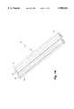
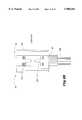
To decrease the weight of an antenna, some systems utilize air loaded transmission lines within the antenna housing to, among other things, transfer radio frequency energy between an input/output connector and each radiating element. Air loaded transmission lines, in general, require some means to suspend a center conductor a predetermined distance away from one or more nearby ground structures to achieve a required characteristic impedance. Past suspension devices invariably introduce dielectric loading to the transmission line which creates undesirable mismatches and losses on the transmission line. To reduce the effects of the mismatches, past systems placed suspension devices at quarter wave intervals along the transmission line so that reflections caused by adjacent devices would cancel. Because this practice generally requires more suspension devices than are needed for supporting/suspending the center conductors, additional weight and signal loss is added to the system.
An important consideration in designing an antenna system for use in a large communication system is ease of installation. As described above, a typical mobile system can require a multitude of antennas to cover a desired service area. Installation and servicing of these antennas can be a monumental task requiring many man-hours of labor with associated labor costs. Therefore, if the complexity of the installation process is reduced, system installation and maintenance costs can be reduced. In addition, a reduction in antenna installation complexity can reduce system installation time and increase installer safety.
SUMMARY OF THE INVENTION
The present invention relates to an antenna system that is particularly suited for use in mobile communications applications. The antenna system is compact and lightweight and is relatively inexpensive and easy to manufacture and install. In addition, the antenna system is relatively linear in operation. The antenna system has a multiple layer design that reduces the overall size of the system and a unique transition for transferring radio frequency energy from one layer to another.
In conceiving of the present invention, it was appreciated that the existence of metal to metal contact in a transmission path, or other high current area, can lead to a nonlinear circuit effect known as passive intermodulation. That is, a diode effect is created at the metal to metal junction that can result in intermodulation products between frequency components in the system. These intermodulation components can create interference between channels in the system and, therefore, are highly undesirable. In accordance with the present invention, metal to metal contact is avoided in high current areas thereby preventing the creation of passive intermods.
In one aspect of the present invention, an antenna system is provided that comprises a transition between layers that does not include metal to metal junctions. More specifically, the antenna system includes: (a) a housing; (b) a ground plane located within the housing and separating a first circuitry layer from a second circuitry layer; (c) a radiating element, having an input/output port, for transferring radio frequency energy in a predetermined operational frequency range between the input/output port and free space, the radiating element being located on the first circuitry layer; (d) a first transmission line, having a first center conductor, for use in transferring radio frequency energy between a first signal node and the input/output port of the radiating element, wherein the first transmission line and the first signal node are located on the first circuitry layer; (c) a second transmission line, having a second center conductor, for use in transferring radio frequency energy between a second signal node and a third signal node, wherein the second transmission line and the second and third signal nodes are located on the second circuitry layer; and (e) a transition for use in transferring radio frequency energy between the first signal node on the first circuitry layer and the second signal node on the second circuitry layer, wherein the transition, the first center conductor, and the second center conductor are collectively formed from a single, homogeneous metallic member having uniform composition.
The radiating element can include any type of radiating structure that is capable of transmitting/receiving radio frequency energy into/from free space. This can include, for example, a dipole, patch, spiral, monopole, loop, horn, helix, doorstop, Vivaldi, and/or notch antenna element. In a preferred embodiment, an air loaded patch is utilized. It should be appreciated that multiple radiating elements, such as in an antenna array, can also be used.
In a preferred embodiment of the present invention, the first transmission line is comprised of a microstrip transmission medium and the second transmission line is comprised of a stripline transmission medium. It should be appreciated, however, that any number of different transmission medium combinations can be implemented in accordance with the present invention.
A mode suppressor is provided for suppressing undesired transmission modes that can originate at the transition. In one embodiment, the mode suppressor includes a grounded conductive member that surrounds the transition on at least three sides. To avoid metal to metal contact, the mode suppressor can be capacitively coupled to the ground plane such that a radio frequency short exists between it and system ground.
The antenna system of the present invention can also include a connector for use in transferring radio frequency energy between the system and an exterior environment. To avoid the creation of metal to metal contact between the center conductor of the connector and a transmission line center conductor within the antenna system, the connector center conductor is capacitively coupled to the transmission line center conductor. In one embodiment, a connector is provided that includes a center conductor having a conductive strip that protrudes out of one end of the connector. A thin dielectric layer is then interposed between the conductive strip and a portion of the transmission line center conductor, thereby capacitively coupling the two structures.
The transmission media used in the antenna system of the present invention are preferably air loaded. In one embodiment of the present invention, a dielectric support means is provided for suspending transmission circuitry, such as a transmission line center conductor, a fixed distance from a ground plane. The support means includes a tapered member that has a relatively wide end for providing strength to the member and a narrow end that contacts the transmission circuitry. Because the end that contacts the transmission circuitry is relatively narrow (i.e., approximately one millimeter or less), the support means produces relatively little dielectric loading on the transmission structure. Because dielectric loading is minimized, support means do not have to be placed at fixed intervals along the transmission structure to reduce reflection. This reduces system cost, weight, and complexity, and simplifies manufacture.
In one embodiment of the antenna system, an adjustable bracket is provided for mounting the system to a vertically oriented support, such as a pole. The bracket includes a first clamp that can be secured to the pole. A brace is also provided that is pivotally connected to the antenna housing and slidably mounted to the first clamp. The bracket also includes fastening means, such as a bolt or screw, for securing the brace with respect to the first clamp. The bracket can also include alignment means, such as an alignment pin, that can temporarily lock the brace in a predetermined position with respect to the first clamp. A second clamp that is pivotally mounted to the housing is also provided.
BRIEF DESCRIPTION OF THE DRAWINGS
FIG. 1a is an isometric view of an antenna system in accordance with the present invention; the antenna system is covered by a radome to protect its internal circuitry;
FIG. 1b is a close up view of an end flange of the antenna system of FIG. 1a;
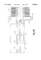
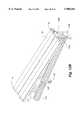
FIGS. 2a and 2b are an isometric view and a top view, respectively, of the antenna system of FIG. 1a with the radome removed;
FIG. 3a is a side view of the antenna system of FIG. 1a with the radome removed, illustrating the multi-layer construction of the antenna system;
FIG. 3b is a blown up portion A-A' of FIG. 3a illustrating the multi-layer construction of the antenna system in more detail;
FIG. 4 is a bottom view of the antenna system of FIG. 1a with a lower ground plane removed illustrating portions of the feed circuitry of the antenna system;
FIG. 5 is an isometric view of a transition for coupling transmission media on the upper and lower layers in accordance with the present invention;
FIGS. 6a, 6b, and 6c are an isometric view, a top view, and a side view, respectively, of a mode suppressor in accordance with the present invention;
FIG. 7 is a side view of the antenna system of FIG. 1a with the radome removed, illustrating the positioning of the mode suppressor of FIGS. 6a, 6b, and 6c between an upper and lower ground plane with a dielectric layer separating the mode suppressor from the ground planes;
FIGS. 8a and 8b are an isometric view and a side view, respectively, illustrating the interconnection between a connector center conductor and a transmission line center conductor in accordance with the present invention; FIG. 8b also illustrates the interconnection between a connector flange and upper and lower ground planes in the antenna system;
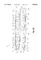
FIGS. 9a and 9b are an isometric view and a side view, respectively, of a retainer for use in holding a transmission line center conductor a predetermined distance from a ground plane in accordance with the present invention;
FIGS. 10a and 10b illustrate the retainer of FIGS. 9a and 9b holding a transmission line center conductor;
FIG. 11 illustrates a spacer that is used to suspend a radiating element above a ground plane in accordance with the present invention;
FIGS. 12a and 12b illustrate a bracketing system that is used to mount the antenna system of FIG. 1 to a pole in accordance with the present invention; and
FIG. 13 illustrates a temporary locking mechanism used in the bracketing system of FIGS. 12a and 12b.
DETAILED DESCRIPTION OF THE PREFERRED EMBODIMENT
The present invention relates to an antenna system that is particularly suited for use in mobile communications applications. The antenna system includes both a transmit array and a receive array in a side by side configuration. In one embodiment, the radiating elements used in each of the arrays consist of air loaded microstrip patch antennas. The elements in each array are linearly arranged and polarization diversity is utilized so that the transmit and receive arrays can be spaced closely together.
FIG. 1a illustrates anantenna system 10 in accordance with the present invention. Theantenna system 10 includes a pair ofend flanges 12, 14 at either end of abody portion 16. During operation of theantenna system 10, thebody portion 16 is surrounded by aradome 18 that protects the circuitry of thesystem 10 from the environment while being relatively transparent to the radio-frequency energy being transmitted/received by theantenna system 10. As illustrated in FIG. 1b,end flange 12 includes a plurality ofconnectors 20, 22 for use in coupling theantenna system 10 to transmit/receive (T/R) circuitry (not shown) external to thesystem 10. The T/R circuitry is operative for creating and delivering transmit signals to a transmit portion of theantenna system 10 and for accepting and processing receive signals from a receive portion of theantenna system 10.
FIGS. 2a and 2b are an isometric view and a top view, respectively, of theantenna system 10 with theradome 18 andend flange 14 removed. In a preferred embodiment, theradome 18 andend flange 14 form an integrated assembly that slides on and off of thebody portion 16 relatively easily. This easy on/off functionality simplifies assembly of thesystem 10 and facilitates servicing of thesystem 10 in the field.
As shown in FIGS. 2a and 2b, theantenna system 10 includes a receivearray portion 24 and a transmitarray portion 26. The receivearray portion 24 includes a linear array ofoctagonal patch elements 28a-28h that operate in a dual slant 45 linearly-polarized mode. The receive array portion also includesfeed structures 32a, 32b (partially shown) for delivering a receive signal from theelements 28a-28h to the receiveconnectors 22. Theelements 28a-28h of the receive array, as well as portions of thefeed structures 32a, 32b, are suspended above aconductive plate 36 that functions as a ground plane and provides structural rigidity to theantenna system 10. Thefeed structures 32a, 32b are comprised of transmission line portions, combiner portions and impedance matching structures.
The transmitarray portion 26 includes a linear array ofrectangular patch elements 30a-30h that operate in a linearly polarized/single pole mode. The transmitarray portion 26 also includes a feed structure 34 (partially shown) for delivering a transmit signal from the transmitconnector 20 to the transmitarray elements 30a-30h. In this regard, thefeed structure 34 includes transmission line sections, divider portions, and impedance matching structures. As with the receivearray portion 24, theelements 30a-30h of the transmitarray portion 26 are suspended above aconductive plate 38. Theconductive plate 38 of the transmitarray portion 26, however, is folded up at the sides to formwalls 40a, 40b on the sides of the transmitarray portion 26. Thewalls 40a, 40b serve to increase the isolation between the transmitarray portion 26 and the receivearray portion 24. Further isolation can also be achieved by adjusting the location of the transmitelements 30a-30h with respect to the receiveelements 28a-28h. For example, with reference to FIG. 2b, the transmit array can be shifted to the right or left to increase isolation. Theconductive plates 36 and 38 are electrically connected to one another and, in one embodiment, the ground surfaces of the two plates are located in substantially the same plane.
To make theantenna system 10 compact, a multi-layer feed arrangement is utilized. That is, a portion of eachfeed structure 32a, 32b, 34 is located on the same layer as theelements 28a-28h, 30a-30h and another portion is located on a different layer than theelements 28a-28h, 30a-30h. FIGS. 3a and 3b are side views of thesystem 10 showing the multi-layer construction, wherein FIG. 3b is a blown up portion A-A' of FIG. 3a. Thesystem 10 has a two layer construction consisting ofupper layer 42 andlower layer 44. As shown, theupper layer 42 includeswall 40b ofconductive plate 38 of the transmitarray portion 26. Theupper layer 42 also includes (although not shown in FIGS. 3a and 3b) all of the antenna elements of thesystem 28a-28h, 30a-30h and upper portions of thefeed structures 32a, 32b, 34. All of the transmission line sections in theupper portion 42 are in microstrip.
Thelower layer 44 includes, among other things, anupper ground plane 46, which is preferably the underside ofconductive plate 38, alower ground plane 48, and lower portions of thefeed structures 32a, 32b, 34. FIG. 4 is a bottom view of thesystem 10, with thelower ground plane 48 removed, illustrating the feed structure portions on thelower layer 44. As illustrated, thelower layer 44 also includes circuitry for connecting thefeed structures 32a, 32b, 34 torespective connectors 20, 22.Center conductor 50, which is suspended betweenupper ground plane 46 andlower ground plane 48, forms a stripline transmission line section on thelower layer 44 as part of thefeed structure 34.
FIG. 5 illustrates a wrap aroundtransition 52 that is used to transfer signals between transmission structures on theupper layer 42 and transmission structures on thelower layer 44. The wrap aroundtransition 52 is a shaped transmission line portion that carries a signal between a transmission line center conductor on theupper layer 42 and a transmission line center conductor on thelower layer 44. The shape of the wrap aroundtransition 52 is preferably arcuate, although other shapes can also be used, such as those including right or acute angles. The width of thetransition 52 is chosen to provide desired impedance characteristics so as to minimize mismatches at the junction points with the transmission line center conductors on the upper and lower layers.
In one embodiment, the wrap aroundtransition 52 is integrally joined to the transmission line center conductors on the upper and lower layers. That is, all three elements are formed together as a single piece, such as by stamping. Thetransition 52 is later shaped by appropriate means before the entire assembly is installed into the antenna housing. By forming thetransition 52 as a single piece with the transmission structures, no metal to metal contact points are created that can result in passive intermodulation problems. As described above, it is very important that passive intermod creation be held to a minimum in communications applications.
As illustrated in FIG. 5, anotch 56 is made in theconductive plate 38 to make room for thetransition 52. The dimensions of thenotch 56 are chosen so that the characteristic impedance of the transmission line is maintained and radiation and mode generation are minimized. A transition, such as the one illustrated in FIG. 5, can be used to transfer radio frequency signals from one transmission medium to another using any one of several combinations. For example, the transition can be between two microstrip media on different layers, between two stripline media on different layers, or, as in the illustrated embodiment, between a microstrip medium on one layer and a stripline medium on another layer.
To prevent the creation of undesired parallel plate transmission modes, or other undesired modes, near thetransition 52 or on thelower layer 44, amode suppressor 58 is located between theupper ground plane 46 and thelower ground plane 48, in the vicinity of thetransition 52. FIGS. 6a-6c illustrate themode suppressor 58 removed from thesystem 10. Themode suppressor 58 includes awalled area 60 that, when installed, substantially surrounds the portion of thetransition 52 that is located in thelower layer 44, on three sides. In a preferred embodiment, the dimensions of thewalled area 60 are chosen so that the length of eachside wall 61a, 61b is approximately two times the spacing between the ground planes 46, 48. In addition, theside walls 61a, 61b of thewalled area 60 in this embodiment extend inward past an endpoint on thetransition 52 by a distance that is greater than or equal to the spacing between the ground planes. Thewalled area 60 must be wide enough to provide an acceptable characteristic impedance for thetransition 52 and so that precise placement of thetransition 52 is not necessary. Thewalled area 60 can be any number of different shapes, such as rectangular (as illustrated in FIGS. 6a-6c) or curved, as long as thetransition 52 is adequately surrounded.
To properly suppress undesired modes, themode suppressor 58 must be grounded (i.e., the mode suppressor must be adequately coupled to the ground planes 46, 48). One way to provide this ground is to directly contact the mode suppressor body to theupper ground plane 46 and thelower ground plane 48. Because themode suppressor 58 is operative in a high current area, however, this direct contact approach can create passive intermodulation problems as described previously. In accordance with one embodiment of the present invention, themode suppressor 58 is capacitively coupled to the upper and lower ground planes 46, 48 to create an RF short between themode suppressor 58 and ground without the need for metal to metal contact.
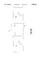
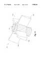
In one embodiment, as illustrated in FIGS. 6a-6c, relativelywide flanges 62a-62d are provided on themode suppressor 58 for creating the capacitive coupling to ground. That is, a suitable dielectric material is interposed between each of theflanges 62a-62d and thecorresponding ground plane 46, 48 for creating a capacitance therebetween. The surface area of eachflange 62a-62d and the dielectric constant and thickness of the dielectric material are chosen to achieve a capacitance that provides substantially a short circuit between the mode suppressor and ground at the frequency of interest. The dielectric material can include an insulative tape that is applied to the mode suppressor and/or the ground planes; a coating on the mode suppressor and/or the ground plane such as, for example, a sprayed-on coating or an anodized layer; or a dielectric sheet material that is laid between themode suppressor 58 and the ground planes 46, 48 during assembly. Other low loss dielectric materials, such as air or teflon, can also be used.
FIG. 7 illustrates themode suppressor 58 installed between the upper and lower ground planes 46, 48 with dielectric layers 66, 68 between themode suppressor 58 and the ground planes 46, 48. Themode suppressor 58 is secured in place using screws, or other suitable fastening means. For example, a screw can be placed through clearance holes in theupper ground plane 46, the upper andlower flanges 62a, 62b of themode suppressor 58, and thelower ground plane 48 and secured with a fastener on the lower side. Alternatively, the fastening method used can be integrated into themode suppressor 58 through injection molding or other methods. For example, an injection molded snap that allows themode suppressor 58 to be snapped in place between the ground planes 46, 48 can be provided. In another alternative embodiment, themode suppressor 58 can be an integral part of the ground plane design, thereby eliminating the need for a separate unit. For example, the walls of themode suppressor 58 can comprise bent portions of the upper and/or lower ground planes 46, 48.
If metallic fasteners are utilized, care must be taken to avoid metal to metal contact that can result in the creation of passive intermodulation components. One way to do this is to provideclearance holes 64 of suitable diameter in the flanges 68a-68d of themode suppressor 58 so that the fasteners never contact the flanges. These clearance holes 64 can be lined with a dielectric material to further isolate them electrically from the fasteners. In addition, dielectric washers or bushings can be provided for preventing electrical contact between the fasteners and the ground planes 46, 48. Other insulating techniques can also be used.
In the illustrated embodiment, spacers 70 are provided for preventing compression of themode suppressor flanges 62a-62d as this compression can significantly change the characteristic impedance in the vicinity of thespacer 70 and/or significantly change the capacitance between theflanges 62a-62d and the ground planes 46, 48 and thus reduce the effectiveness of themode suppressor 58 and thetransition 52. Thespacers 70 can be separate units or integral to themode suppressor 58. Alternatively, theflanges 62a-62d of themode suppressor 58 can be solid from top to bottom so that compression is avoided.
FIG. 8a is an isometric view illustrating the interconnection between thecenter conductor 72 of transmitconnector 20 and transmissionline center conductor 76 of transmitfeed structure 34. A similar interconnection method is used between the center conductors of receiveconnectors 22 and transmission line center conductors within receive feed structure 32. As in other portions of thesystem 10, the method of interconnecting theconnector center conductor 72 to the transmissionline center conductor 76 avoids the creation of metal to metal contact, and hence the creation of intermodulation products, by using capacitive coupling. For example, as seen in FIG. 8a, a firstconductive strip 78, that is conductively coupled to theconnector center conductor 72, is situated above a secondconductive strip 80, that is an extension of transmissionline center conductor 76, with adielectric layer 82 disposed therebetween. The surface area of the first and secondconductive strips 78, 80 and the type and thickness of the dielectric comprisingdielectric layer 82 determine the capacitance between theconductive strips 78, 80. In general, the capacitance required between theconductive strips 78, 80 must be enough to create substantially an RF short circuit at the frequency of interest. That is, the reactance formed by the capacitor should not exceed a relatively low value, such as approximately 0.05 ohms, at the frequency of interest.
In a preferred embodiment,conductive strip 78 forms a single piece withconnector center conductor 72, such that no metal to metal contact is made at the junction. That is, theconnector center conductor 72 and theconductive strip 78 are formed from the same piece of metal and assembled into the connected 20 by the connector manufacturer. Alternatively, theconductive strip 78 can be attached to theconnector center conductor 72 by other means, such as by welding, after manufacture of theconnector 20.
It is very important that moisture is not allowed to collect betweenconductive strip 78 andconductive strip 80. This could significantly change the capacitance between the two conductive strips, thereby creating undesired mismatches at the input to theantenna system 10. To avoid moisture collection, and to provide support to the junction, a shrink wrap covering is placed around the junction between thestrips 78, 80. In one embodiment, a shrink wrap having an inner adhesive lining is used to provide an enhanced moisture seal at the junction. The shrink wrap covering can be extended to cover the area whereconductive strip 78 joins withconnector center conductor 72. The covering can also be extended in the other direction to cover a significant portion of transmissionline center conductor 76.
FIG. 8b is a side view illustrating the interconnection betweenconnector center conductor 72 and transmissionline center conductor 76. FIG. 8b also illustrates the interconnection betweenflange 84 ofconnector 20 and upper and lower ground planes 46, 48 oflower layer 44. Because this is a high current area, metal to metal contact should be avoided when connecting theconnector flange 84 to the ground planes 46, 48. In this regard, a capacitive coupling is implemented in this area. First,flange extension plates 88, 92 are provided that extend the flange in the direction of the upper and lower ground planes 46, 48. Theseflange extension plates 88, 92 are substantially parallel to the ground planes 46, 48 and are separated by a distance that allows them to fit closely around the ground planes. Theflange extension plates 88, 92 are preferably formed from a single piece of metal with theconnector flange 84 to avoid metal to metal contact. However, they can also be welded or soldered to theconnector flange 84. To provide capacitive coupling, adielectric layer 86 is interposed betweenextension plate 88 andupper ground plane 46 and adielectric layer 90 is interposed betweenextension plate 92 andlower ground plane 48.
FIGS. 9A and 9B illustrate aretainer 94 for use in suspending thefeed structures 32a, 32b, 34 above their respectiveconductive plates 36, 38. Theretainer 94 includes anupper arm 96 and alower arm 98 that extend radially from abody 100. Theupper arm 96 and thelower arm 98 each include a retainingfin 102, 104 for use in holding a transmission line center conductor, or other circuitry, at a proper layer above an associated ground plane. To reduce dielectric loading on the transmission line, retainingfins 102, 104 are tapered so that the portion that contacts the transmission line center conductor comprises very little dielectric material while the wider portion increases the strength and rigidity of the fin. FIG. 9b is a sectional view illustrating the tapered cross section of the retainingfins 102, 104. Because the contact area between the retainingfins 102, 104 and the transmission line center conductor is very small, very little moisture can accumulate at the junction. This is important as moisture can significantly affect the characteristic impedance of the transmission line. Theretainer 94 also includes a retaininglip 106 for preventing a transmission line semi-conductor from sliding laterally outward from between retainingfins 102 and 104.
To secure theretainer 94 to a base plate, fastening means 108 is provided. In a preferred embodiment of the invention, fastening means 108 comprises a compression snap that is pressed into a proper receptacle in the base plate. However, fastening means 108 can include virtually any type of fastening means, such as, for example, a screw that can be screwed into a tapped hole in the base plate.
As is apparent,retainer 94 should be constructed of a dielectric material having relatively low loss. The dielectric material should be relatively rigid so that upper andlower arms 96, 98 can provide adequate support to the transmission line center conductor being held. In addition, the material used should not be moisture absorbing, as this can change the dielectric loss characteristics of the material significantly. In one embodiment of the invention, a nylon glass material is used. Materials such as acetal, nylon 66, and polyethylene, for example, can also be used.
Because theretainer 94 of the present invention creates very little dielectric loading on the transmission line it is holding, relatively little reflection is created at the portion of the transmission line being held. In addition, because reflections are so small, retainers do not need to be periodically placed along the transmission line to cancel mismatch effects. This significantly reduces the number of retainers that are needed to support the transmission line and correspondingly reduces the overall weight of and losses in theantenna system 10. Theretainer 94 can also be used to support the feed structures on thelower layer 44 so that these feed structures are at the proper position between the upper and lower ground planes 46, 48. When used on the lower layer, the retainers can include fastening means on both the top and the bottom ofretainer body 100. FIGS. 10A and 10B are two views of aretainer 94 secured to aconductive plate 38 and holding a transmission line center conductor.
FIG. 11 illustrates aspacer 110 that is used to suspend theradiating elements 28a-28h, 30a-30h above their respectiveconductive plates 36, 38. Thespacer 110 includes four radially extendingarms 112a-112d that provide most of the support to the radiating element. Thearms 112a-112d have a tapered structure much like that of the retainingfins 102, 104 of theretainer 94. This tapered structure reduces the dielectric loading on the radiating element and also prevents a collection of moisture between thespacer 110 and the radiating element that can adversely affect operation. Thespacer 110 should be made of a similar dielectric material to that of theretainer 94. In the illustrated embodiment, aclearance hole 114 is provided in thespacer 110 for use in securing the spacer between the radiating element and the associated conductive plate. That is, a screw, or other fastening means, is inserted through a hole in the radiating element and throughhole 114 ofspacer 110 after which it is secured to the underlying base plate or other structure. It should be appreciated that other fastening methods can be utilized for securing thespacer 110 in the proper position between the radiating element and the corresponding conductive plate without departing from the spirit and scope of the invention. For example, thespacer 110 can be molded with two threaded posts, one on the top and one on the bottom, for use in securing thespacer 110 in position. The posts are placed through the holes in the radiating element and the base plate and a fastener is secured to the end.
FIG. 12a illustrates abracketing system 110 that is used to mount theantenna system 10 to a pole. Thebracketing system 110 includes a pair of clam-shell type clamps, i.e.,upper clamp 113a andlower clamp 113b, for attachment to the pole. Thebracketing system 110 also includes abrace 114 that, when installed, is connected between theupper clamp 113a and theend flange 14 of theantenna system 10. Thebrace 114 is used in adjusting the angle of theantenna system 10 with respect to the pole. Thebrace 114 includes a pair of slots 118a, 118b machined into side flanges 120a, 120b at one end of thebrace 114. The slots 118a, 118b ride alongbolts 122 secured to ears/flanges on theupper clamp 113a. Thebolts 122 can be tightened to fix the position of thebrace 114 with respect to theupper clamp 113a. Both thebrace 114 and thelower clamp 113b includeflanges 122a, 122b and 124a, 124b for use in pivotally connecting each unit to theantenna system 10.
Theclamps 113a, 113b each have a special adjustable hinge mechanism that allows the clamp to be attached to poles of varying diameter. For example, one embodiment of the clamp is capable of being attached to poles having diameters ranging from two to four inches. To accommodate varying pole diameters, eachclamp 113a, 113b is comprised of a first andsecond jaw member 126a, 126b. Thefirst jaw member 126a has a plurality ofhub locations 128 to which the second jaw member can be attached. Adjustment for pole diameter is accomplished by attaching thesecond jaw member 126b to theappropriate hub location 128 on thefirst jaw member 126a. To secure one of the clamps 113a, 113b to the pole, the hinge mechanism is first appropriately adjusted for the pole and then the clamp is placed around the pole at the appropriate location. A bolt is then placed through a clearance hole in thefirst jaw member 126a of the clamp and is secured to a lock nut welded onto the second jaw member of the clamp.Teeth 130 are provided on the contact surfaces of the first andsecond jaw members 126a, 126b to prevent slippage of the clamp on the pole once secured in place.
FIG. 12b illustrates theantenna system 10 mounted on apole 116 usingbracketing system 110. As illustrated, thelower clamp 113b is pivotally connected to theend flange 12 atpivot points 132a, 132b. This pivotal connection allows the angle between theantenna system 10 and thepole 116 to be varied. In one embodiment, thebracketing system 110 is capable setting the angle of theantenna system 10 from +2 degrees from vertical to -10 degrees from vertical for a vertically oriented pole. In addition, although not shown in FIG. 12b, thebrace 114 is pivotally connected to endflange 14 of theantenna system 10.
FIG. 13 is a close up view of a temporary locking feature that is used for locking the position of thebrace 114 with respect to theclamp 113a during installation. Although only one side of the clamp/brace assembly is shown, it should be understood that both sides can include the locking feature. The locking feature greatly simplifies the installation process by reducing the effort required to correctly position the clamps 113a, 113b on the pole. Thebrace 114 and theupper clamp 113a each include an alignment hole having a diameter that is tailored to receive analignment pin 134. The alignment holes are located so that, when aligned with one another using thealignment pin 134, thebrace 114 is locked in a particular position with respect to theupper clamp 113a. Because thebrace 114 is locked in position with respect to theupper clamp 113a, the distance between theclamps 113a, 113b is preset and a technician only needs to set the appropriate azimuth angle of theantenna system 10 and tighten the bolts on the clamps. After the twoclamps 113a, 113b are properly positioned and secured to thepole 116, thealignment pin 134 can be removed and the elevation angle of theantenna system 10 can be adjusted. An angle indicator is machined into thebrace 114 to simplify the angle adjustment. Once the proper angle is set, thebolts 122 are tightened to fix the elevation angle of theantenna system 10. In a preferred embodiment, the alignment holes are located so that alignment sets theantenna system 10 in a vertical position (i.e., zero degrees with respect to the pole 116) when the clamps are properly secured to thepole 116.
Although the present invention has been described in conjunction with its preferred embodiments, it is to be understood that modifications and variations may be resorted to without departing from the spirit and scope of the invention as those skilled in the art readily understand. Such modifications and variations are considered to be within the purview and scope of the invention and the appended claims.

Claims (11)

What is claimed is:
1. An antenna system comprising:
a housing;
a ground plane located within said housing and separating a first circuitry layer from a second circuitry layer;
a radiating element, having an input/output port, for transferring radio frequency energy in a predetermined operational frequency range between said input/output port and free space, said radiating element being located on said first circuitry layer;
a first transmission line, having a first center conductor, for use in transferring radio frequency energy between a first signal node and said input/output port of said radiating element, wherein said first transmission line and said first signal node are located on said first circuitry layer;
a second transmission line, having a second center conductor, for use in transferring radio frequency energy between a second signal node and a third signal node, wherein said second transmission line and said second and third signal nodes are located on said second circuitry layer; and
a transition for use in transferring radio frequency energy between said first signal node on said first circuitry layer and said second signal node on said second circuitry layer, wherein said transition, said first center conductor, and said second center conductor are collectively formed from a single, homogeneous metallic member having substantially uniform composition.
2. The antenna system of claim 1, further comprising:
a connector, coupled to said housing, for use in transferring radio frequency energy between said antenna system and an exterior environment, said connector having a connector center conductor; and
a third transmission line, having a third center conductor, for use in transferring radio frequency energy between said connector and said third signal node;
wherein said connector center conductor is capacitively coupled to said third center conductor.
3. The antenna system of claim 1, further comprising:
dielectric support means for use in suspending transmission circuitry a substantially fixed perpendicular distance from said ground plane, said support means including at least one tapered support member having a wide end and a narrow end, wherein said narrow end contacts said transmission circuitry.
4. The antenna system of claim 1, further comprising:
an adjustable bracket, coupled to said housing, for use in mounting said antenna system to a vertically oriented support, said bracket including:
a first clamp capable of being fixedly attached to said vertically oriented support;
a brace having a first end and a second end, said brace being pivotally mounted to said housing at said first end and slidably mounted to said first clamp at said second end; and
fastening means for securing said brace in a substantially fixed position with respect to said first clamp so that said antenna housing can be fixed at a desired angle with respect to said vertically oriented support.
5. The antenna system of claim 4, further comprising:
alignment means for temporarily locking said brace in a predetermined fixed position with respect to said first clamp during an initial installation period, wherein said alignment means is capable of rapid disengagement.
6. The antenna system of claim 4, further comprising:
a second clamp capable of being fixedly attached to said vertically oriented support, said second clamp being pivotally mounted to said housing.
7. The antenna system of claim 1, wherein:
said second transmission line comprises one of the following: a microstrip transmission line and a stripline transmission line.
8. The antenna system of claim 1, further comprising:
a mode suppressor, separate from said transition, for suppressing undesired transmission modes originating at said transition.
9. The antenna system of claim 8, wherein:
said mode suppressor comprises a conductive member that surrounds said transition on at least three sides.
10. The antenna system of claim 8, wherein:
said mode suppressor is substantially short circuited to ground in said predetermined operational frequency range of said radiating element.
11. The antenna system of claim 8, wherein said mode suppressor is capacitively coupled to ground.
US08/842,3751997-04-231997-04-23Antenna systemExpired - Fee RelatedUS5905465A (en)

Priority Applications (10)

Application NumberPriority DateFiling DateTitle
US08/842,375US5905465A (en)1997-04-231997-04-23Antenna system
AU71312/98AAU735881B2 (en)1997-04-231998-04-17Antenna system
KR1019997009796AKR20010020214A (en)1997-04-231998-04-17Antenna System
PCT/US1998/007790WO1998048480A1 (en)1997-04-231998-04-17Antenna system
CA002287357ACA2287357A1 (en)1997-04-231998-04-17Antenna system
CN98800487ACN1223018A (en)1997-04-231998-04-17 antenna system
IL13245898AIL132458A0 (en)1997-04-231998-04-17Antenna system
EP98918375AEP0985249A4 (en)1997-04-231998-04-17Antenna system
JP54619398AJP2001522549A (en)1997-04-231998-04-17 Antenna system
NO995155ANO995155L (en)1997-04-231999-10-22 antenna System

Applications Claiming Priority (1)

Application NumberPriority DateFiling DateTitle
US08/842,375US5905465A (en)1997-04-231997-04-23Antenna system

Publications (1)

Publication NumberPublication Date
US5905465Atrue US5905465A (en)1999-05-18

Family

ID=25287159

Family Applications (1)

Application NumberTitlePriority DateFiling Date
US08/842,375Expired - Fee RelatedUS5905465A (en)1997-04-231997-04-23Antenna system

Country Status (10)

CountryLink
US (1)US5905465A (en)
EP (1)EP0985249A4 (en)
JP (1)JP2001522549A (en)
KR (1)KR20010020214A (en)
CN (1)CN1223018A (en)
AU (1)AU735881B2 (en)
CA (1)CA2287357A1 (en)
IL (1)IL132458A0 (en)
NO (1)NO995155L (en)
WO (1)WO1998048480A1 (en)

Cited By (31)

* Cited by examiner, † Cited by third party
Publication numberPriority datePublication dateAssigneeTitle
WO2001086754A1 (en)*2000-05-052001-11-15Nokia CorporationBase station of a communication network, preferably of a mobile telecommunication network
US6366254B1 (en)2000-03-152002-04-02Hrl Laboratories, LlcPlanar antenna with switched beam diversity for interference reduction in a mobile environment
US6396456B1 (en)*2001-01-312002-05-28Tantivy Communications, Inc.Stacked dipole antenna for use in wireless communications systems
WO2002089248A1 (en)*2001-04-302002-11-07Mission Telecom, Inc.A broadband dual-polarized microstrip array antenna
US20030048226A1 (en)*2001-01-312003-03-13Tantivy Communications, Inc.Antenna for array applications
US20030122721A1 (en)*2001-12-272003-07-03Hrl Laboratories, LlcRF MEMs-tuned slot antenna and a method of making same
US20030227351A1 (en)*2002-05-152003-12-11Hrl Laboratories, LlcSingle-pole multi-throw switch having low parasitic reactance, and an antenna incorporating the same
US20040135649A1 (en)*2002-05-152004-07-15Sievenpiper Daniel FSingle-pole multi-throw switch having low parasitic reactance, and an antenna incorporating the same
US20040227583A1 (en)*2003-05-122004-11-18Hrl Laboratories, LlcRF MEMS switch with integrated impedance matching structure
US20040227667A1 (en)*2003-05-122004-11-18Hrl Laboratories, LlcMeta-element antenna and array
US20040227668A1 (en)*2003-05-122004-11-18Hrl Laboratories, LlcSteerable leaky wave antenna capable of both forward and backward radiation
US20040227678A1 (en)*2003-05-122004-11-18Hrl Laboratories, LlcCompact tunable antenna
US20040263408A1 (en)*2003-05-122004-12-30Hrl Laboratories, LlcAdaptive beam forming antenna system using a tunable impedance surface
US7154451B1 (en)2004-09-172006-12-26Hrl Laboratories, LlcLarge aperture rectenna based on planar lens structures
US7307589B1 (en)2005-12-292007-12-11Hrl Laboratories, LlcLarge-scale adaptive surface sensor arrays
US7456803B1 (en)2003-05-122008-11-25Hrl Laboratories, LlcLarge aperture rectenna based on planar lens structures
US7868829B1 (en)2008-03-212011-01-11Hrl Laboratories, LlcReflectarray
US7898482B2 (en)*2008-04-242011-03-01Sirit Technologies Inc.Conducting radio frequency signals using multiple layers
US8212739B2 (en)2007-05-152012-07-03Hrl Laboratories, LlcMultiband tunable impedance surface
US8436785B1 (en)2010-11-032013-05-07Hrl Laboratories, LlcElectrically tunable surface impedance structure with suppressed backward wave
US8876549B2 (en)2010-11-222014-11-04Andrew LlcCapacitively coupled flat conductor connector
US8982011B1 (en)2011-09-232015-03-17Hrl Laboratories, LlcConformal antennas for mitigation of structural blockage
US8994609B2 (en)2011-09-232015-03-31Hrl Laboratories, LlcConformal surface wave feed
US20150188231A1 (en)*2013-12-262015-07-02ThalesCompact antenna structure for satellite telecommunications
US9219461B2 (en)2011-12-222015-12-22Commscope Technologies LlcCapacitive blind-mate module interconnection
US9466887B2 (en)2010-11-032016-10-11Hrl Laboratories, LlcLow cost, 2D, electronically-steerable, artificial-impedance-surface antenna
US20170179589A1 (en)*2014-09-052017-06-22Kmw Inc.Antenna device for mobile communication system
US10056701B2 (en)*2016-04-292018-08-21Laird Technologies, Inc.Multiband WiFi directional antennas
JP2020114027A (en)*2016-09-232020-07-27日本ピラー工業株式会社Planar antenna and antenna device
US10790576B2 (en)*2015-12-142020-09-29Commscope Technologies LlcMulti-band base station antennas having multi-layer feed boards
US11184049B2 (en)*2018-08-102021-11-23Ball Aerospace & Technologies Corp.Systems and methods for signal isolation in radio frequency circuit boards

Families Citing this family (9)

* Cited by examiner, † Cited by third party
Publication numberPriority datePublication dateAssigneeTitle
DE19823750A1 (en)*1998-05-271999-12-09Kathrein Werke Kg Antenna array with several primary radiator modules arranged vertically one above the other
DE19823749C2 (en)1998-05-272002-07-11Kathrein Werke Kg Dual polarized multi-range antenna
DE10012809A1 (en)2000-03-162001-09-27Kathrein Werke KgDual polarized dipole array antenna has supply cable fed to supply point on one of two opposing parallel dipoles, connecting cable to supply point on opposing dipole
DE10064129B4 (en)2000-12-212006-04-20Kathrein-Werke Kg Antenna, in particular mobile radio antenna
DE10150150B4 (en)2001-10-112006-10-05Kathrein-Werke Kg Dual polarized antenna array
CN101030672B (en)*2007-03-092014-09-24清华大学 Mobile Terminal Four Antenna System
JP2013098927A (en)*2011-11-042013-05-20Ricoh Co LtdCoil antenna, coil antenna mounting body, manufacturing method of coil antenna, and manufacturing method of coil antenna mounting body
WO2022050690A1 (en)*2020-09-022022-03-10이돈신High-performance mobile communication antenna device
KR102234539B1 (en)*2020-09-022021-03-31이돈신High performance mobile communication transceiver base station antenna apparatus

Citations (16)

* Cited by examiner, † Cited by third party
Publication numberPriority datePublication dateAssigneeTitle
US3887925A (en)*1973-07-311975-06-03IttLinearly polarized phased antenna array
USRE29911E (en)*1973-04-171979-02-13Ball CorporationMicrostrip antenna structures and arrays
US4291312A (en)*1977-09-281981-09-22The United States Of America As Represented By The Secretary Of The NavyDual ground plane coplanar fed microstrip antennas
US4614947A (en)*1983-04-221986-09-30U.S. Philips CorporationPlanar high-frequency antenna having a network of fully suspended-substrate microstrip transmission lines
US4772890A (en)*1985-03-051988-09-20Sperry CorporationMulti-band planar antenna array
US4825220A (en)*1986-11-261989-04-25General Electric CompanyMicrostrip fed printed dipole with an integral balun
US4829314A (en)*1985-12-201989-05-09U.S. Philips CorporationMicrowave plane antenna simultaneously receiving two polarizations
US4829309A (en)*1986-08-141989-05-09Matsushita Electric Works, Ltd.Planar antenna
US4914449A (en)*1987-11-301990-04-03Sony CorporationMicrowave antenna structure with intergral radome and rear cover
US4973972A (en)*1989-09-071990-11-27The United States Of America As Represented By The Administrator Of The National Aeronautics And Space AdminstrationStripline feed for a microstrip array of patch elements with teardrop shaped probes
US5216430A (en)*1990-12-271993-06-01General Electric CompanyLow impedance printed circuit radiating element
US5285212A (en)*1992-09-181994-02-08Radiation Systems, Inc.Self-supporting columnar antenna array
US5499033A (en)*1993-07-021996-03-12Northern Telecom LimitedPolarization diversity antenna
US5565877A (en)*1994-09-231996-10-15Andrew CorporationUltra-high frequency, slot coupled, low-cost antenna system
US5596337A (en)*1994-02-281997-01-21Hazeltine CorporationSlot array antennas
US5742258A (en)*1995-08-221998-04-21Hazeltine CorporationLow intermodulation electromagnetic feed cellular antennas

Family Cites Families (5)

* Cited by examiner, † Cited by third party
Publication numberPriority datePublication dateAssigneeTitle
GB2189080B (en)*1986-04-021989-11-29Thorn Emi Electronics LtdMicrostrip antenna
FR2651926B1 (en)*1989-09-111991-12-13Alcatel Espace FLAT ANTENNA.
US5438697A (en)*1992-04-231995-08-01M/A-Com, Inc.Microstrip circuit assembly and components therefor
JPH08222940A (en)*1995-02-141996-08-30Mitsubishi Electric Corp Antenna device
GB2337861B (en)*1995-06-022000-02-23Dsc CommunicationsIntegrated directional antenna

Patent Citations (16)

* Cited by examiner, † Cited by third party
Publication numberPriority datePublication dateAssigneeTitle
USRE29911E (en)*1973-04-171979-02-13Ball CorporationMicrostrip antenna structures and arrays
US3887925A (en)*1973-07-311975-06-03IttLinearly polarized phased antenna array
US4291312A (en)*1977-09-281981-09-22The United States Of America As Represented By The Secretary Of The NavyDual ground plane coplanar fed microstrip antennas
US4614947A (en)*1983-04-221986-09-30U.S. Philips CorporationPlanar high-frequency antenna having a network of fully suspended-substrate microstrip transmission lines
US4772890A (en)*1985-03-051988-09-20Sperry CorporationMulti-band planar antenna array
US4829314A (en)*1985-12-201989-05-09U.S. Philips CorporationMicrowave plane antenna simultaneously receiving two polarizations
US4829309A (en)*1986-08-141989-05-09Matsushita Electric Works, Ltd.Planar antenna
US4825220A (en)*1986-11-261989-04-25General Electric CompanyMicrostrip fed printed dipole with an integral balun
US4914449A (en)*1987-11-301990-04-03Sony CorporationMicrowave antenna structure with intergral radome and rear cover
US4973972A (en)*1989-09-071990-11-27The United States Of America As Represented By The Administrator Of The National Aeronautics And Space AdminstrationStripline feed for a microstrip array of patch elements with teardrop shaped probes
US5216430A (en)*1990-12-271993-06-01General Electric CompanyLow impedance printed circuit radiating element
US5285212A (en)*1992-09-181994-02-08Radiation Systems, Inc.Self-supporting columnar antenna array
US5499033A (en)*1993-07-021996-03-12Northern Telecom LimitedPolarization diversity antenna
US5596337A (en)*1994-02-281997-01-21Hazeltine CorporationSlot array antennas
US5565877A (en)*1994-09-231996-10-15Andrew CorporationUltra-high frequency, slot coupled, low-cost antenna system
US5742258A (en)*1995-08-221998-04-21Hazeltine CorporationLow intermodulation electromagnetic feed cellular antennas

Cited By (44)

* Cited by examiner, † Cited by third party
Publication numberPriority datePublication dateAssigneeTitle
US6366254B1 (en)2000-03-152002-04-02Hrl Laboratories, LlcPlanar antenna with switched beam diversity for interference reduction in a mobile environment
US7277728B1 (en)*2000-05-052007-10-02Nokia CorporationBase station of a communication network, preferably of a mobile telecommunication network
WO2001086754A1 (en)*2000-05-052001-11-15Nokia CorporationBase station of a communication network, preferably of a mobile telecommunication network
US6396456B1 (en)*2001-01-312002-05-28Tantivy Communications, Inc.Stacked dipole antenna for use in wireless communications systems
US20030048226A1 (en)*2001-01-312003-03-13Tantivy Communications, Inc.Antenna for array applications
WO2002089248A1 (en)*2001-04-302002-11-07Mission Telecom, Inc.A broadband dual-polarized microstrip array antenna
US20040119645A1 (en)*2001-04-302004-06-24Lee Byung-JeBroadband dual-polarized microstrip array antenna
US6956528B2 (en)2001-04-302005-10-18Mission Telecom, Inc.Broadband dual-polarized microstrip array antenna
US20030122721A1 (en)*2001-12-272003-07-03Hrl Laboratories, LlcRF MEMs-tuned slot antenna and a method of making same
US6864848B2 (en)2001-12-272005-03-08Hrl Laboratories, LlcRF MEMs-tuned slot antenna and a method of making same
US20030227351A1 (en)*2002-05-152003-12-11Hrl Laboratories, LlcSingle-pole multi-throw switch having low parasitic reactance, and an antenna incorporating the same
US7298228B2 (en)2002-05-152007-11-20Hrl Laboratories, LlcSingle-pole multi-throw switch having low parasitic reactance, and an antenna incorporating the same
US7276990B2 (en)2002-05-152007-10-02Hrl Laboratories, LlcSingle-pole multi-throw switch having low parasitic reactance, and an antenna incorporating the same
US20040135649A1 (en)*2002-05-152004-07-15Sievenpiper Daniel FSingle-pole multi-throw switch having low parasitic reactance, and an antenna incorporating the same
US20040227668A1 (en)*2003-05-122004-11-18Hrl Laboratories, LlcSteerable leaky wave antenna capable of both forward and backward radiation
US20040263408A1 (en)*2003-05-122004-12-30Hrl Laboratories, LlcAdaptive beam forming antenna system using a tunable impedance surface
US7068234B2 (en)2003-05-122006-06-27Hrl Laboratories, LlcMeta-element antenna and array
US7071888B2 (en)2003-05-122006-07-04Hrl Laboratories, LlcSteerable leaky wave antenna capable of both forward and backward radiation
US7164387B2 (en)2003-05-122007-01-16Hrl Laboratories, LlcCompact tunable antenna
US7245269B2 (en)2003-05-122007-07-17Hrl Laboratories, LlcAdaptive beam forming antenna system using a tunable impedance surface
US7253699B2 (en)2003-05-122007-08-07Hrl Laboratories, LlcRF MEMS switch with integrated impedance matching structure
US20040227678A1 (en)*2003-05-122004-11-18Hrl Laboratories, LlcCompact tunable antenna
US20040227667A1 (en)*2003-05-122004-11-18Hrl Laboratories, LlcMeta-element antenna and array
US20040227583A1 (en)*2003-05-122004-11-18Hrl Laboratories, LlcRF MEMS switch with integrated impedance matching structure
US7456803B1 (en)2003-05-122008-11-25Hrl Laboratories, LlcLarge aperture rectenna based on planar lens structures
US7154451B1 (en)2004-09-172006-12-26Hrl Laboratories, LlcLarge aperture rectenna based on planar lens structures
US7307589B1 (en)2005-12-292007-12-11Hrl Laboratories, LlcLarge-scale adaptive surface sensor arrays
US8212739B2 (en)2007-05-152012-07-03Hrl Laboratories, LlcMultiband tunable impedance surface
US7868829B1 (en)2008-03-212011-01-11Hrl Laboratories, LlcReflectarray
US7898482B2 (en)*2008-04-242011-03-01Sirit Technologies Inc.Conducting radio frequency signals using multiple layers
US9466887B2 (en)2010-11-032016-10-11Hrl Laboratories, LlcLow cost, 2D, electronically-steerable, artificial-impedance-surface antenna
US8436785B1 (en)2010-11-032013-05-07Hrl Laboratories, LlcElectrically tunable surface impedance structure with suppressed backward wave
US8876549B2 (en)2010-11-222014-11-04Andrew LlcCapacitively coupled flat conductor connector
US8982011B1 (en)2011-09-232015-03-17Hrl Laboratories, LlcConformal antennas for mitigation of structural blockage
US8994609B2 (en)2011-09-232015-03-31Hrl Laboratories, LlcConformal surface wave feed
US9219461B2 (en)2011-12-222015-12-22Commscope Technologies LlcCapacitive blind-mate module interconnection
US20150188231A1 (en)*2013-12-262015-07-02ThalesCompact antenna structure for satellite telecommunications
US9515383B2 (en)*2013-12-262016-12-06ThalesCompact antenna structure for satellite telecommunications
US20170179589A1 (en)*2014-09-052017-06-22Kmw Inc.Antenna device for mobile communication system
US10608331B2 (en)*2014-09-052020-03-31Kmw Inc.Antenna device for mobile communication system
US10790576B2 (en)*2015-12-142020-09-29Commscope Technologies LlcMulti-band base station antennas having multi-layer feed boards
US10056701B2 (en)*2016-04-292018-08-21Laird Technologies, Inc.Multiband WiFi directional antennas
JP2020114027A (en)*2016-09-232020-07-27日本ピラー工業株式会社Planar antenna and antenna device
US11184049B2 (en)*2018-08-102021-11-23Ball Aerospace & Technologies Corp.Systems and methods for signal isolation in radio frequency circuit boards

Also Published As

Publication numberPublication date
KR20010020214A (en)2001-03-15
CN1223018A (en)1999-07-14
WO1998048480A1 (en)1998-10-29
AU735881B2 (en)2001-07-19
AU7131298A (en)1998-11-13
JP2001522549A (en)2001-11-13
CA2287357A1 (en)1998-10-29
NO995155D0 (en)1999-10-22
IL132458A0 (en)2001-03-19
EP0985249A1 (en)2000-03-15
NO995155L (en)1999-12-17
EP0985249A4 (en)2001-01-17

Similar Documents

PublicationPublication DateTitle
US5905465A (en)Antenna system
US6317099B1 (en)Folded dipole antenna
US6650301B1 (en)Single piece twin folded dipole antenna
US5726666A (en)Omnidirectional antenna with single feedpoint
US6285336B1 (en)Folded dipole antenna
US6344833B1 (en)Adjusted directivity dielectric resonator antenna
US5892482A (en)Antenna mutual coupling neutralizer
US6822618B2 (en)Folded dipole antenna, coaxial to microstrip transition, and retaining element
US6037912A (en)Low profile bi-directional antenna
US5929822A (en)Low intermodulation electromagnetic feed cellular antennas
AU778969B2 (en)Folded dipole antenna
US6281858B1 (en)High performance, directional cellular band antenna
US5339089A (en)Antenna structure
KR100492207B1 (en) Log cycle dipole antenna with internal center feed microstrip feed line
WO1997048148A1 (en)Conformal antenna assemblies
AU624342B2 (en)Microwave antenna structure
US5999141A (en)Enclosed dipole antenna and feeder system
US8159406B2 (en)Phased-array antenna radiator for a super economical broadcast system
US5440319A (en)Integrated microwave antenna/downconverter
US6801789B1 (en)Multiple-beam antenna
WO2024015132A1 (en)Antenna filter units for base station antennas and related radio adaptor boards
US5793258A (en)Low cross polarization and broad bandwidth
US20250149770A1 (en)Clamping apparatus for support pole of radio unit
AU756868B2 (en)Log periodic dipole antenna

Legal Events

DateCodeTitleDescription
ASAssignment

Owner name:BALL AEROSPACE AND TECHNOLOGIES CORPORATION, COLOR

Free format text:ASSIGNMENT OF ASSIGNORS INTEREST;ASSIGNORS:OLSON, STEVEN C.;STEWART, KERRY R.;GOODWIN, JEFFREY DAVID;AND OTHERS;REEL/FRAME:008750/0906

Effective date:19970725

ASAssignment

Owner name:ARC WIRELESS SOLUTIONS, INC., A CORP. OF UTAH, COL

Free format text:ASSIGNMENT OF ASSIGNORS INTEREST;ASSIGNOR:BALL AEROSPACE & TECHNOLOGIES CORP., A CORP. OF DELAWARE;REEL/FRAME:013077/0944

Effective date:20010821

REMIMaintenance fee reminder mailed
LAPSLapse for failure to pay maintenance fees
STCHInformation on status: patent discontinuation

Free format text:PATENT EXPIRED DUE TO NONPAYMENT OF MAINTENANCE FEES UNDER 37 CFR 1.362

FPLapsed due to failure to pay maintenance fee

Effective date:20030518

ASAssignment

Owner name:RBS CITIZENS, N.A., MASSACHUSETTS

Free format text:SECURITY INTEREST;ASSIGNORS:ARC GROUP WORLDWIDE, INC.;FLOMET LLC;TEKNA SEAL LLC;REEL/FRAME:032695/0878

Effective date:20140407

Owner name:ARC GROUP WORLDWIDE, INC., FLORIDA

Free format text:CHANGE OF NAME;ASSIGNOR:ARC WIRELESS SOLUTIONS, INC.;REEL/FRAME:032712/0668

Effective date:20120807

ASAssignment

Owner name:ARC WIRELESS, INC., FLORIDA

Free format text:ASSIGNMENT OF ASSIGNORS INTEREST;ASSIGNOR:ARC GROUP WORLDWIDE, INC.;REEL/FRAME:032760/0180

Effective date:20140424

ASAssignment

Owner name:RBS CITIZENS, N.A., MASSACHUSETTS

Free format text:SECURITY INTEREST;ASSIGNOR:ARC WIRELESS, INC.;REEL/FRAME:032839/0130

Effective date:20140424

ASAssignment

Owner name:ARC GROUP WORLDWIDE, INC., FLORIDA

Free format text:RELEASE BY SECURED PARTY;ASSIGNOR:CITIZENS BANK, N.A., AS SUCCESSOR TO RBS CITIZENS, N.A.;REEL/FRAME:051495/0763

Effective date:20191227

Owner name:TEKNA SEAL LLC, CONNECTICUT

Free format text:RELEASE BY SECURED PARTY;ASSIGNOR:CITIZENS BANK, N.A., AS SUCCESSOR TO RBS CITIZENS, N.A.;REEL/FRAME:051495/0763

Effective date:20191227

Owner name:FLOMET LLC, FLORIDA

Free format text:RELEASE BY SECURED PARTY;ASSIGNOR:CITIZENS BANK, N.A., AS SUCCESSOR TO RBS CITIZENS, N.A.;REEL/FRAME:051495/0763

Effective date:20191227

Owner name:ARC WIRELESS, INC., FLORIDA

Free format text:RELEASE BY SECURED PARTY;ASSIGNOR:CITIZENS BANK, N.A., AS SUCCESSOR TO RBS CITIZENS, N.A.;REEL/FRAME:051495/0924

Effective date:20191227


[8]ページ先頭

©2009-2025 Movatter.jp